EP2395571B1 - Organic electronic device comprising an organic semiconducting material - Google Patents
Organic electronic device comprising an organic semiconducting material Download PDFInfo
- Publication number
- EP2395571B1 EP2395571B1 EP10165537.1A EP10165537A EP2395571B1 EP 2395571 B1 EP2395571 B1 EP 2395571B1 EP 10165537 A EP10165537 A EP 10165537A EP 2395571 B1 EP2395571 B1 EP 2395571B1
- Authority
- EP
- European Patent Office
- Prior art keywords
- organic
- electronic device
- doped
- layer
- organic electronic
- Prior art date
- Legal status (The legal status is an assumption and is not a legal conclusion. Google has not performed a legal analysis and makes no representation as to the accuracy of the status listed.)
- Active
Links
Images
Classifications
-
- H—ELECTRICITY
- H10—SEMICONDUCTOR DEVICES; ELECTRIC SOLID-STATE DEVICES NOT OTHERWISE PROVIDED FOR
- H10K—ORGANIC ELECTRIC SOLID-STATE DEVICES
- H10K85/00—Organic materials used in the body or electrodes of devices covered by this subclass
- H10K85/60—Organic compounds having low molecular weight
- H10K85/615—Polycyclic condensed aromatic hydrocarbons, e.g. anthracene
- H10K85/622—Polycyclic condensed aromatic hydrocarbons, e.g. anthracene containing four rings, e.g. pyrene
-
- H—ELECTRICITY
- H10—SEMICONDUCTOR DEVICES; ELECTRIC SOLID-STATE DEVICES NOT OTHERWISE PROVIDED FOR
- H10K—ORGANIC ELECTRIC SOLID-STATE DEVICES
- H10K50/00—Organic light-emitting devices
- H10K50/10—OLEDs or polymer light-emitting diodes [PLED]
- H10K50/11—OLEDs or polymer light-emitting diodes [PLED] characterised by the electroluminescent [EL] layers
- H10K50/12—OLEDs or polymer light-emitting diodes [PLED] characterised by the electroluminescent [EL] layers comprising dopants
- H10K50/121—OLEDs or polymer light-emitting diodes [PLED] characterised by the electroluminescent [EL] layers comprising dopants for assisting energy transfer, e.g. sensitization
-
- H—ELECTRICITY
- H10—SEMICONDUCTOR DEVICES; ELECTRIC SOLID-STATE DEVICES NOT OTHERWISE PROVIDED FOR
- H10K—ORGANIC ELECTRIC SOLID-STATE DEVICES
- H10K50/00—Organic light-emitting devices
- H10K50/10—OLEDs or polymer light-emitting diodes [PLED]
- H10K50/14—Carrier transporting layers
-
- H—ELECTRICITY
- H10—SEMICONDUCTOR DEVICES; ELECTRIC SOLID-STATE DEVICES NOT OTHERWISE PROVIDED FOR
- H10K—ORGANIC ELECTRIC SOLID-STATE DEVICES
- H10K71/00—Manufacture or treatment specially adapted for the organic devices covered by this subclass
- H10K71/30—Doping active layers, e.g. electron transporting layers
-
- H—ELECTRICITY
- H10—SEMICONDUCTOR DEVICES; ELECTRIC SOLID-STATE DEVICES NOT OTHERWISE PROVIDED FOR
- H10K—ORGANIC ELECTRIC SOLID-STATE DEVICES
- H10K85/00—Organic materials used in the body or electrodes of devices covered by this subclass
- H10K85/60—Organic compounds having low molecular weight
- H10K85/649—Aromatic compounds comprising a hetero atom
- H10K85/656—Aromatic compounds comprising a hetero atom comprising two or more different heteroatoms per ring
-
- H—ELECTRICITY
- H10—SEMICONDUCTOR DEVICES; ELECTRIC SOLID-STATE DEVICES NOT OTHERWISE PROVIDED FOR
- H10K—ORGANIC ELECTRIC SOLID-STATE DEVICES
- H10K85/00—Organic materials used in the body or electrodes of devices covered by this subclass
- H10K85/60—Organic compounds having low molecular weight
- H10K85/649—Aromatic compounds comprising a hetero atom
- H10K85/657—Polycyclic condensed heteroaromatic hydrocarbons
- H10K85/6572—Polycyclic condensed heteroaromatic hydrocarbons comprising only nitrogen in the heteroaromatic polycondensed ring system, e.g. phenanthroline or carbazole
-
- H—ELECTRICITY
- H10—SEMICONDUCTOR DEVICES; ELECTRIC SOLID-STATE DEVICES NOT OTHERWISE PROVIDED FOR
- H10K—ORGANIC ELECTRIC SOLID-STATE DEVICES
- H10K50/00—Organic light-emitting devices
- H10K50/10—OLEDs or polymer light-emitting diodes [PLED]
- H10K50/14—Carrier transporting layers
- H10K50/15—Hole transporting layers
- H10K50/155—Hole transporting layers comprising dopants
-
- H—ELECTRICITY
- H10—SEMICONDUCTOR DEVICES; ELECTRIC SOLID-STATE DEVICES NOT OTHERWISE PROVIDED FOR
- H10K—ORGANIC ELECTRIC SOLID-STATE DEVICES
- H10K50/00—Organic light-emitting devices
- H10K50/10—OLEDs or polymer light-emitting diodes [PLED]
- H10K50/14—Carrier transporting layers
- H10K50/16—Electron transporting layers
- H10K50/165—Electron transporting layers comprising dopants
-
- Y—GENERAL TAGGING OF NEW TECHNOLOGICAL DEVELOPMENTS; GENERAL TAGGING OF CROSS-SECTIONAL TECHNOLOGIES SPANNING OVER SEVERAL SECTIONS OF THE IPC; TECHNICAL SUBJECTS COVERED BY FORMER USPC CROSS-REFERENCE ART COLLECTIONS [XRACs] AND DIGESTS
- Y10—TECHNICAL SUBJECTS COVERED BY FORMER USPC
- Y10S—TECHNICAL SUBJECTS COVERED BY FORMER USPC CROSS-REFERENCE ART COLLECTIONS [XRACs] AND DIGESTS
- Y10S428/00—Stock material or miscellaneous articles
- Y10S428/917—Electroluminescent
Definitions
- the present invention relates to an organic semiconducting layer, preferably an organic electronic device, comprising an organic semiconducting material.
- Organic semiconductors can be used to fabricate simple electronic components e.g. resistors, diodes, field effect transistors, and also optoelectronic components like organic light emitting devices (e.g. OLED), and many others.
- OLED organic light emitting devices
- Conjugated organic compounds can be small molecules, for instance monomers, or oligomers, polymers, copolymers, copolymers of conjugated and non-conjugated blocks, completely or partially cross-linked layers, aggregate structures, or brush like structures.
- Organic electronic semiconductors can also be used in organic electronic devices, and in organic-inorganic hybrid devices.
- Typical organic semiconducting compounds may have a gap that is still high enough so that the compounds are optically active.
- Organic field effect transistors are explained, for example, in US7026643 , US2005146262 and US2008230776 .
- the resistance of a semiconductive layer that is contacted by two electrodes (source and drain) can be controlled by the voltage that is applied to the gate.
- the gate is displaced on an insulator that is displaced parallel in contact to the semiconductive layer.
- Various geometries can be used, such as bottom gate (on the substrate), top gate (on the opposite side of the semiconductive layer relative to the substrate) or on both sides.
- Many different arrangements of layers can be used such as bipolar layers, injection layer, insulating layer between electrode and semiconductive layer to lower the off current, etc.
- OTFTs organic thin-film transistors
- Transparent circuits such as transparent OTFTs require that the high mobility organic material also comprises a wide electronic band gap; the electric injection of holes and / or electrons must be still provided.
- OLEDs require transparent transport layers, with high conductivity. The transparency is necessary in those opto-electric devices to avoid non desired absorption of the light. These so called “window” materials can be used as transport layers, exciton or charge blocking layers. The thickness of the layers made with the window materials is used to adjust the micro cavity of the OLEDs in such a way that the outcoupled emission of the OLED is a maximum.
- the non-optically active layers of all kinds of semiconductor devices can be exchanged for window materials in order to fabricate fully transparent components and circuits (e.g US20060033115 ). The functionality and nomenclature of the layers are typical as used in the field. Further explanation can be found in US2006244370 .
- Electronic devices also need high stability towards temperature, meaning that the intrinsic properties of the amorphous organic semiconducting materials, such as triphenyl amine derivatives, or phenantronine derivatives, must include a high glass transition temperature (Tg) and high temperature stability in the device.
- Tg glass transition temperature
- the performance characteristics of (opto)electronic multilayered components are determined by the ability of the layers to transport the charge carriers, amongst others.
- the ohmic losses in the charge transport layers during operation are associated with their conductivity.
- the conductivity directly influences the operating voltage required and also determines the thermal load of the component.
- a bending of the band in the vicinity of a metal contact results which simplifies the injection of charge carriers and can therefore reduce the contact resistance.
- doped charge-carrier transport layers p-doping of the hole transport layer by admixture of acceptor-like molecules, n-doping of the electron transport layer by admixture of donor-like molecules
- US2008203406 and US 5,093,698 The use of doped charge-carrier transport layers (p-doping of the hole transport layer by admixture of acceptor-like molecules, n-doping of the electron transport layer by admixture of donor-like molecules) in organic light-emitting diodes is described in US2008203406 and US 5,093,698 .
- US2008227979 discloses in detail the doping of organic transport materials, also called matrix, with inorganic and with organic dopants. Basically, an effective electronic transfer occurs from the dopant to the matrix increasing the Fermi level of the matrix.
- the LUMO energy level of the dopant must be more negative than the HOMO energy level of the matrix or at least slightly more positive, not more than 0.5 eV, to the HOMO energy level of the matrix.
- the HOMO energy level of the dopant must be more positive than the LUMO energy level of the matrix or at least slightly more negative, not lower than 0.5 eV, to the LUMO energy level of the matrix. It is furthermore desired that the energy level difference for energy transfer from dopant to matrix is smaller than +0.3 eV.
- CuPc copperphthalocyanine
- F4TCNQ tetrafluoro-tetracyanoquinonedimethane
- ZnPc zincphthalocyanine
- HOMO -5.2 eV
- a-NPD N,N'-Bis(naphthalen-1-yl)-N,N-bis(phenyl)-benzidine
- Typical examples of doped electron transport materials are: fullerene C60 doped with acridine orange base (AOB); perylene-3,4,9,10-tetracarboxylic-3,4,9,10-dianhydride (PTCDA) doped with leuco crystal violet; 2,9 - di (phenanthren-9-yl) - 4,7 - diphenyl - 1,10 - phenanthroline doped with tetrakis ( 1,3,4,6,7,8 - hexahydro - 2H - pyrimido [ 1,2 - a] pyrimidinato) ditungsten (II) (W(hpp) 4 ); naphthalene tetracarboxylic acid di-anhydride (NTCDA) doped with 3,6-bis-(dimethyl amino)-acridine; NTCDA doped with bis(ethylene-dithio) tetrathiafulvalene (BEDT-TTF).
- ETM electron transport materials
- EMH emitter host
- an object of the present invention to provide a semiconducting layer, preferably an organic electronic device, comprising a specific class of functional materials which can be utilized as organic semiconducting materials to overcome the drawbacks of the prior art.
- an organic electronic device shall be provided comprising transparent organic semiconducting materials which are additionally thermally stable and/or dopable. Further, the organic electronic device shall comprise semiconducting materials which can be synthesized without any difficulties.
- Organic electronic device comprising an organic semiconducting material comprising at least one compound according to the following formula (I):
- Ar and R 1-4 are independently selected from C 6 -C 20 -aryl and C 5 -C 20 -heteroaryl.
- heteroaryl is a C5-C20 condensed ring structure in which one or two C are substituted by N or S.
- R 5 is H and combines with Ar to a moiety selected from
- Ar is selected from
- the device is an electronic, optoelectronic or electroluminescent device having an electronically functionally effective region, wherein the electronically effective region comprises at least one compound according to formula (I) as defined above.
- the device has a layered structure and at least one layer comprises at least one compound according to formula (I) as defined above.
- the organic semiconducting material is doped by an n-dopant.
- the device with a layered structure has at least two layers of the organic semiconducting material comprising a compound of formula (I), one n-doped and the other undoped. Preferably both layers are in direct contact.
- the organic semiconducting material may be doped by an organic n-dopant which dopant has HOMO energy level which is more positive than -3.3 eV.
- the device may be preferably an organic light-emitting diode, a field-effect transistor, a sensor, a photodetector, an organic thin-film transistor, an organic integrated circuit, an organic light-emitting transistor, a light-emitting electrochemical cell or an organic laser diode. It was found out that the organic semiconducting materials comprising a compound of formula (I) are especially suitable to be used in electron transport layers in OLEDs.
- Ar can be selected from a number of differently substituted or unsubstituted C 6 -C 20 -aryl or C 5 -C 20 -heteroaryl.
- Suitable substituents may be for example halogen, such as Br, Aryl, such as pyrene, or CF 3 .
- An organic n-dopant can be, for example, selected from the dopants as disclosed in EP 2002492 A1 , US 2007252140 or US 2009212280 .
- an organic electronic device comprising an organic semiconducting material comprising at least one organic matrix material which is optionally doped with at least one dopant, wherein the matrix material comprises a compound according to formula (1).
- the compounds can be used in electron transport layers, which might be optionally doped.
- the compounds can be also used in light-emitting diodes in interlayers such as hole blocking layers.
- the compounds are preferably used in the electron transport layer and not as main compound of the emitter layer, preferably they are not used in the emitter layer at all.
- a window semiconducting organic material is provided for the device that can be electrically doped achieving a high conductivity while it remains highly transparent in the visible spectra and has a high thermal stability.
- an organic field-effect transistor comprising at least one compound according to formula (I) for use in a transport layer, in other words, in the semiconducting channel layer.
- An organic field effect transistor may also comprise at least one compound as disclosed as electronically inert buffer layer, when no charge is injected due to high potential barrier.
- An organic field effect transistor may also comprise at least one compound as disclosed as doped injection layer.
- the compounds used in this invention according to formula (I) can be used in OLEDs in electron transport layers as a neat layer, or as a doped layer in combination with a redox dopant.
- the compounds can also be used in mixture with other electron transport materials, with other hole transport materials or with other functional materials such as emitter dopants.
- the compounds can be used as hole blocking layers. Advantageous effects are seen over the prior art since the materials have a higher glass transition temperature compared to materials described in the prior art, such as in DE 10 2007 012 794 or EP 07 400 033.2 (not published yet).
- the use of the compounds according to formula (I) provides high thermal stability, especially due to high glass transition temperature, a good LUMO position for organic light-emitting devices, good dopability, conductivity and charge carrier mobility, high transparency, and easy synthesis. Further, preparation of these compounds can be conducted in a very cost-effective manner. Finally, it can be pointed out that the synthesis of such compounds offers a high flexibility to change independently the R and X, Ar 1 or Ar 2 groups which opens access to more complex compounds and therefore to different physical/chemical properties resulting in a fine tuning thereof.
- HOMO highest occupied molecular orbital energy level
- LUMO lowest unoccupied molecular orbital energy level
- IP ionization potentials
- UPS ultraviolet photo spectroscopy
- IPES inverted photo electron spectroscopy
- EA electron affinity
- IPES inverted photo electron spectroscopy
- EA electron affinity
- Electrochemical measurements in solution are an alternative to the determination of solid state oxidation (Eox) and reduction (Ered) potential.
- An adequate method is for example the cyclo-voltammetry.
- Hole transport layers including the respective blockers, mostly have HOMO in the range from -4.5 to -5.5 eV (below the vacuum level) and LUMO in the range of -1.5 eV to -3 eV.
- the HOMO levels of the emitter materials are in the range of -5 eV to -6.5 eV, and the LUMO in the range from -2 to -3 eV.
- Electron transport materials, including their respective blockers have their HOMO in a range of -5.5 eV to -6.8 eV and LUMO in the range of -2.3 eV to -3.3 eV.
- the work function of the contact materials is around -4 to -5 eV for the anode and -3 to -4.5 eV for the cathode.
- the dopant donor is a molecule or a neutral radical or combination thereof with a HOMO energy level (ionization potential in solid state) more positive than -3.3 eV, preferably more positive than -2.8 eV, more preferably more positive than -2.6 eV.
- the HOMO of the donor can be estimated by cyclo-voltammetric measurements.
- An alternative way to measure the reduction potential is to measure the cation of the donor salt.
- the donor has to exhibit an oxidation potential that is smaller than or equal to -1.5 V vs Fc / Fc+ (Ferrum/Ferrocenium redox-pair), preferably smaller than -1.5 V, more preferably smaller than or equal to approximately -2.0 V, even more preferably smaller than or equal to -2.2 V.
- the molar mass of the donor is in a range between 100 and 2000 g/mol, preferably in a range from 200 and 1000 g / mol.
- the molar doping concentration is in the range of 1:10000 (dopant molecule : matrix molecule) and 1:2, preferably between 1:100 and 1:5, more preferably between 1:100 and 1:10. In individual cases doping concentrations larger than 1:2 are applied, e.g.
- the donor can be created by a precursor during the layer forming (deposition) process or during a subsequent process of layer formation (see DE 10307125.3 ).
- the above given value of the HOMO level of the donor refers to the resulting molecule or molecule radical.
- a dopant acceptor is a molecule or a neutral radical or combination thereof with a LUMO level more negative than -4.5 eV, preferably more negative than -4.8 eV, more preferably more negative than -5.04 eV.
- the LUMO of the acceptor can be estimated by cyclo-voltammetric measurements.
- the acceptor has to exhibit a reduction potential that is larger than or equal to approximately -0.3 V vs Fc / Fc+ Ferrocene/Ferrocenium redox-pair), preferably larger than or equal to 0.0 V, preferably larger than or equal to 0.24 V.
- the molar mass of the aceptor is preferably in the range of 100 to 2000 g / mol, more preferably between 200 and 1000 g / mol, and even more preferably between 300 g/mol and 2000 g/mol.
- the molar doping concentration is in the range of 1:10000 (dopant molecule : matrix molecule) and 1:2, preferably between 1:100 and 1:5, more preferably between 1:100 and 1:10. In individual cases doping concentrations larger than 1:2 are applied, e.g. if large conductivities are required.
- the acceptor can be created by a precursor during the layer forming (deposition) process or during a subsequent process of layer formation.
- the above given value of the LUMO level of the acceptor refers to the resulting molecule or molecule radical.
- doping electrical doping as explained above.
- This doping can also be called redox-doping or charge transfer doping. It is known that the doping increases the density of charge carriers of a semiconducting matrix towards the charge carrier density of the undoped matrix.
- An electrically doped semiconductor layer also has an increased effective mobility in comparison with the undoped semiconductor matrix.
- the conductivity can be, for example, measured by the so-called 2-point or 4-point-method.
- contacts of a conductive material such as gold or indium-tin-oxide
- the thin film to be examined is applied onto the substrate, so that the contacts are covered by the thin film.
- the current is measured. From the geometry of the contacts and the thickness of the sample the resistance and therefore the conductivity of the thin film material can be determined.
- the four point or two point method give the same conductivity values for doped layers since the doped layers grant a good ohmic contact.
- the temperature stability can also be measured with that method in which the (undoped or doped) layer is heated stepwise, and after a waiting period, the conductivity is measured.
- the maximum temperature which can be applied to the layer without loosing the desired semiconducting properties, is then the temperature just before the conductivity breaks down.
- a doped layer can be heated on the substrate with two electrodes, as disclosed above, in steps of 1°C, wherein after each step there is a waiting period of 10 seconds. Then the conductivity is measured.
- the conductivity changes with temperature and breaks down abruptly at a particular temperature.
- the temperature stability is therefore the temperature up to which the conductivity does not break down abruptly.
- the measurement is performed in vacuum.
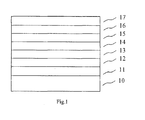
- Fig. 1 shows a cross section of a typical exemplary small molecule OLED.
- the organic electronic device of the present invention may be an organic light emitting diode.
- Fig. 1 shows a typical layer structure of an organic light emitting diode.
- the layers are disposed on a substrate (10) in the following order: anode (11), p-doped hole transport layer (12), electron blocking layer (13), emission layer (14), hole blocking layer (15), n-electron transport layer (16), and cathode (17).
- Two or more layers can collapse into a smaller number of layers if properties can be combined.
- Inverted structure and multiple stacked OLEDs are also well known in the field.
- the emission layer is usually composed by an emitter matrix material and an emitter dopant; this layer can be also composed by several other layers to generate light with a broad spectrum combining several emitters, for example, to generate white light.
- R's in the above general synthesis scheme shall stand for R 1-4 according to formula (I).
- Ar shall in this general synthesis scheme be understood to stand for the moiety "Ar-R 5 " according to formual (I).
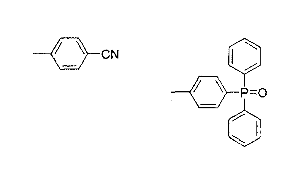
- Second step Synthesis of 7-phenyl-5,6,8,9-tetrahydrodihenzo[c,h]acridine (2). All manipulations were carried out under argon.
- Second step Synthesis of 7-(4-bromophenyl)-5,6,8,9-tetrahydrodibenzo[c,h]acridine (5). All manipulations were carried out under argon.
- Second step Synthesis of 7-(3-bromophenyl)-5,6,8,9-tetrahydrodibenzo[c,b]acridine (9). All manipulations were carried out under argon.
- the conductivity of a doped layer consisting of material of structure 18 in table 1 doped with 5% of W(hpp)4 was measured at room temperature and was 3x10 -7 S/cm.
- the conductivity of a doped layer consisting of material of structure 3 in table 1 doped with 5% of W(hpp)4 was measured at room temperature and was 1.2x10 -5 S/cm.
- the conductivity of a doped layer consisting of material of structure 2 in table 1 doped with 5% of W(hpp)4 was measured at room temperature and was 9.95x10 -6 S/cm.
- An OLED was fabricated with the following procedure: A glass substrate coated with ITO (90 nm thick, pre-patterned) was cleaned in organic solvents in conventional ultra-sound. Afterwards the substrate was treated with ozone plasma for 5 minutes. After the cleaning, the substrate was transferred to vacuum. The organic layers were deposited in high vacuum (base pressure lower than 10 -3 Pa) by conventional VTE (Vacuum thermal evaporation). The deposited area was defined by a shadow mask, keeping some area of the ITO surface free so that an electrical contact for the measurements could (later on) be established.
- the organic layer sequence over the ITO layer is: 50 nm thick NPD layer doped with F4TCNQ; 10 nm thick non-doped NPD layer, 20 nm blue emitter host layer doped with a fluorescent emitter; 10 nm ETL (structure 4), 60 nm ETL (structure 4) doped with W(hpp) 4 (5% in weight).
- a 100 nm aluminum layer was deposited as cathode.
- the OLED reached 1000 cd/m 2 at 3.59 V.
- An OLED was fabricated with the following procedure: A glass substrate coated with ITO (90 nm thick, pre-patterned) was cleaned in organic solvents in conventional ultra-sound. Afterwards the substrate was treated with ozone plasma for 5 minutes. After the cleaning, the substrate was transferred to vacuum. The organic layers were deposited in high vacuum (base pressure lower than 10 -3 Pa) by conventional VTE (Vacuum thermal evaporation). The deposited area was defined by a shadow mask, keeping some area of the ITO surface free so that an electrical contact for the measurements could (later on) be established.
- the organic layer sequence over the ITO layer is: 50 nm thick NPD layer doped with F4TCNQ; 10 nm thick non-doped NPD layer, 20 nm blue emitter host layer doped with a fluorescent emitter; 10 nm ETL (structure Ib), 60 nm ETL (structure 1b) doped with W(hpp) 4 (5% in weight).
- a 100 nm aluminum layer was deposited as cathode.
- the OLED reached 1000 cd/m 2 at 4.25 V.
Landscapes
- Physics & Mathematics (AREA)
- Engineering & Computer Science (AREA)
- Spectroscopy & Molecular Physics (AREA)
- Chemical & Material Sciences (AREA)
- Materials Engineering (AREA)
- Optics & Photonics (AREA)
- Manufacturing & Machinery (AREA)
- Electroluminescent Light Sources (AREA)
- Other In-Based Heterocyclic Compounds (AREA)
- Plural Heterocyclic Compounds (AREA)
Description
- The present invention relates to an organic semiconducting layer, preferably an organic electronic device, comprising an organic semiconducting material.
- Conjugated organic compounds have different applications. One important field comprises organic semiconductors. Organic semiconductors can be used to fabricate simple electronic components e.g. resistors, diodes, field effect transistors, and also optoelectronic components like organic light emitting devices (e.g. OLED), and many others. The industrial and economical significance of the organic semiconductors and their devices is reflected in the increased number of devices using organic semiconducting active layers and the increasing industry focus on the subject.
- A simple OLED is demonstrated in
US4356429A . There, between conductive electrodes, two semiconductive organic layers are brought together: one transporting holes and the other one transporting electrons. The recombination of holes and electrons forms excitons in one or both of the organic layers, the excitons are eventually emitted following the spin statistics. Excitons with triplet spin can also be harvested by using the materials and techniques described inEP1705727 . More elaborated OLEDs are described inEP1804309 andUS2008182129 . - Conjugated organic compounds can be small molecules, for instance monomers, or oligomers, polymers, copolymers, copolymers of conjugated and non-conjugated blocks, completely or partially cross-linked layers, aggregate structures, or brush like structures. A device made with different types of compounds, in different layers or mixed together, for example with polymer and small molecule layers, is also called a polymer - small molecule hybrid device. Organic electronic semiconductors can also be used in organic electronic devices, and in organic-inorganic hybrid devices.
- Despite the large electronic gap, usually up to 3 eV, formed between the highest occupied molecular orbital (HOMO) and the lowest unoccupied molecular orbital (LUMO) of the molecule, it is normally still low enough such that both positive and negative charge carriers can be injected by special electrodes. Typical organic semiconducting compounds may have a gap that is still high enough so that the compounds are optically active.
- Organic field effect transistors are explained, for example, in
US7026643 ,US2005146262 andUS2008230776 . The resistance of a semiconductive layer that is contacted by two electrodes (source and drain) can be controlled by the voltage that is applied to the gate. The gate is displaced on an insulator that is displaced parallel in contact to the semiconductive layer. Various geometries can be used, such as bottom gate (on the substrate), top gate (on the opposite side of the semiconductive layer relative to the substrate) or on both sides. Many different arrangements of layers can be used such as bipolar layers, injection layer, insulating layer between electrode and semiconductive layer to lower the off current, etc. - Different functional layers in different organic semiconductor devices request a variety of special characteristics.
- For instance organic thin-film transistors (OTFTs) need high mobility materials in their active channel. Transparent circuits, such as transparent OTFTs require that the high mobility organic material also comprises a wide electronic band gap; the electric injection of holes and / or electrons must be still provided.
- OLEDs require transparent transport layers, with high conductivity. The transparency is necessary in those opto-electric devices to avoid non desired absorption of the light. These so called "window" materials can be used as transport layers, exciton or charge blocking layers. The thickness of the layers made with the window materials is used to adjust the micro cavity of the OLEDs in such a way that the outcoupled emission of the OLED is a maximum. The non-optically active layers of all kinds of semiconductor devices can be exchanged for window materials in order to fabricate fully transparent components and circuits (e.g
US20060033115 ). The functionality and nomenclature of the layers are typical as used in the field. Further explanation can be found inUS2006244370 . - Electronic devices also need high stability towards temperature, meaning that the intrinsic properties of the amorphous organic semiconducting materials, such as triphenyl amine derivatives, or phenantronine derivatives, must include a high glass transition temperature (Tg) and high temperature stability in the device.
- The performance characteristics of (opto)electronic multilayered components are determined by the ability of the layers to transport the charge carriers, amongst others. In the case of light-emitting diodes, the ohmic losses in the charge transport layers during operation are associated with their conductivity. The conductivity directly influences the operating voltage required and also determines the thermal load of the component. Furthermore, depending on the charge carrier concentration in the organic layers, a bending of the band in the vicinity of a metal contact results which simplifies the injection of charge carriers and can therefore reduce the contact resistance.
- By electrically doping hole transport layers with a suitable acceptor material (p-doping) or electron transport layers with a donor material (n-doping), respectively, the density of charge carriers in organic solids (and therefore the conductivity) can be increased substantially. Additionally, analogous to the experience with inorganic semiconductors, applications can be anticipated which are precisely based on the use of p- and n-doped layers in a component and otherwise would be not conceivable. The use of doped charge-carrier transport layers (p-doping of the hole transport layer by admixture of acceptor-like molecules, n-doping of the electron transport layer by admixture of donor-like molecules) in organic light-emitting diodes is described in
US2008203406 andUS 5,093,698 . -
US2008227979 discloses in detail the doping of organic transport materials, also called matrix, with inorganic and with organic dopants. Basically, an effective electronic transfer occurs from the dopant to the matrix increasing the Fermi level of the matrix. For an efficient transfer in a p-doping case, the LUMO energy level of the dopant must be more negative than the HOMO energy level of the matrix or at least slightly more positive, not more than 0.5 eV, to the HOMO energy level of the matrix. For the n-doping case, the HOMO energy level of the dopant must be more positive than the LUMO energy level of the matrix or at least slightly more negative, not lower than 0.5 eV, to the LUMO energy level of the matrix. It is furthermore desired that the energy level difference for energy transfer from dopant to matrix is smaller than +0.3 eV. - Typical examples of doped hole transport materials are: copperphthalocyanine (CuPc), which HOMO level is approximately -5.2 eV, doped with tetrafluoro-tetracyanoquinonedimethane (F4TCNQ), which LUMO level is about -5.2 eV; zincphthalocyanine (ZnPc) (HOMO = -5.2 eV) doped with F4TCNQ; a-NPD (N,N'-Bis(naphthalen-1-yl)-N,N-bis(phenyl)-benzidine) doped with F4TCNQ.
- Typical examples of doped electron transport materials are: fullerene C60 doped with acridine orange base (AOB); perylene-3,4,9,10-tetracarboxylic-3,4,9,10-dianhydride (PTCDA) doped with leuco crystal violet; 2,9 - di (phenanthren-9-yl) - 4,7 - diphenyl - 1,10 - phenanthroline doped with tetrakis ( 1,3,4,6,7,8 - hexahydro - 2H - pyrimido [ 1,2 - a] pyrimidinato) ditungsten (II) (W(hpp)4); naphthalene tetracarboxylic acid di-anhydride (NTCDA) doped with 3,6-bis-(dimethyl amino)-acridine; NTCDA doped with bis(ethylene-dithio) tetrathiafulvalene (BEDT-TTF).
- There is a technical challenge to provide electron transport materials (ETM) and emitter host (EMH) materials that have a sufficiently low laying LUMO level so that they can be doped, and still have a high enough laying LUMO level which can efficiently transfer charge to emitter host (in case of an ETM) and transfer energy to the emitter dopant (in case of EMH). The limitation for high laying LUMO level of the ETL is given by the dopability, since the n-dopants with very high HOMO tend to be unstable; also the injection is difficult for very high LUMO of the ETL.
- It is an object of the present invention to provide a semiconducting layer, preferably an organic electronic device, comprising a specific class of functional materials which can be utilized as organic semiconducting materials to overcome the drawbacks of the prior art. Especially, an organic electronic device shall be provided comprising transparent organic semiconducting materials which are additionally thermally stable and/or dopable. Further, the organic electronic device shall comprise semiconducting materials which can be synthesized without any difficulties.
- This object is achieved by an Organic electronic device comprising an organic semiconducting material comprising at least one compound according to the following formula (I):

- wherein R1-4 are independently selected from H, halogen, CN, substituted or unsubstituted C1-C20-alkyl or heteroalkyl, C6-C20-aryl or C5-C20-heteroaryl, C1-C20-alkoxy or C6-C20-aryloxy,
- Ar is selected from substituted or unsubstituted C6-C20-aryl or C5-C20-heteroaryl, and
- R5 is selected from substituted or unsubstituted C6-C20-aryl or C5-C20-heteroaryl, H or
- Preferably, Ar and R1-4 are independently selected from C6-C20-aryl and C5-C20-heteroaryl.
- More preferably heteroaryl is a C5-C20 condensed ring structure in which one or two C are substituted by N or S.
- In a further preferred embodiment, R5 is H and combines with Ar to a moiety selected from


- In a further preferred embodiment, Ar is selected from


- It is preferred that the device is an electronic, optoelectronic or electroluminescent device having an electronically functionally effective region, wherein the electronically effective region comprises at least one compound according to formula (I) as defined above.
- Even preferred, the device has a layered structure and at least one layer comprises at least one compound according to formula (I) as defined above.
- Most preferred, the organic semiconducting material is doped by an n-dopant.
- In another embodiment, the device with a layered structure has at least two layers of the organic semiconducting material comprising a compound of formula (I), one n-doped and the other undoped. Preferably both layers are in direct contact.
- The organic semiconducting material may be doped by an organic n-dopant which dopant has HOMO energy level which is more positive than -3.3 eV.
- The device may be preferably an organic light-emitting diode, a field-effect transistor, a sensor, a photodetector, an organic thin-film transistor, an organic integrated circuit, an organic light-emitting transistor, a light-emitting electrochemical cell or an organic laser diode. It was found out that the organic semiconducting materials comprising a compound of formula (I) are especially suitable to be used in electron transport layers in OLEDs.
- Most preferred structures of the compound of formula (I) can be as follows in table 1:

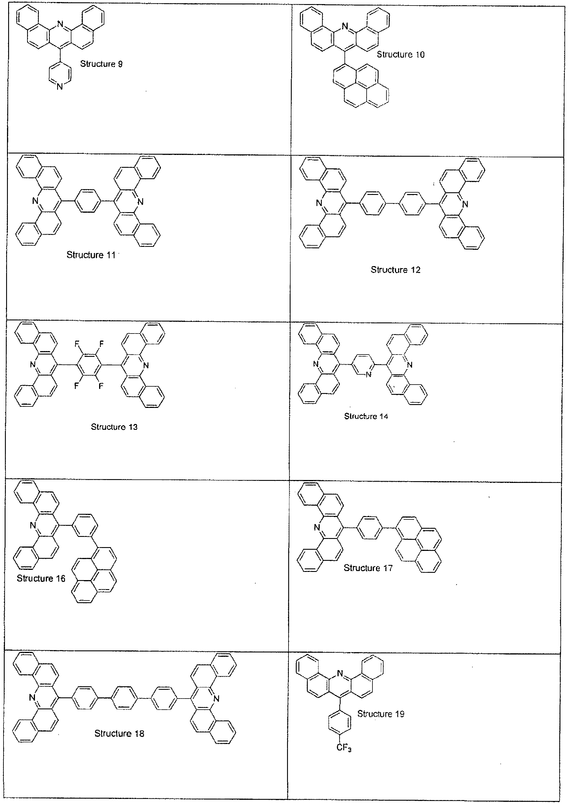
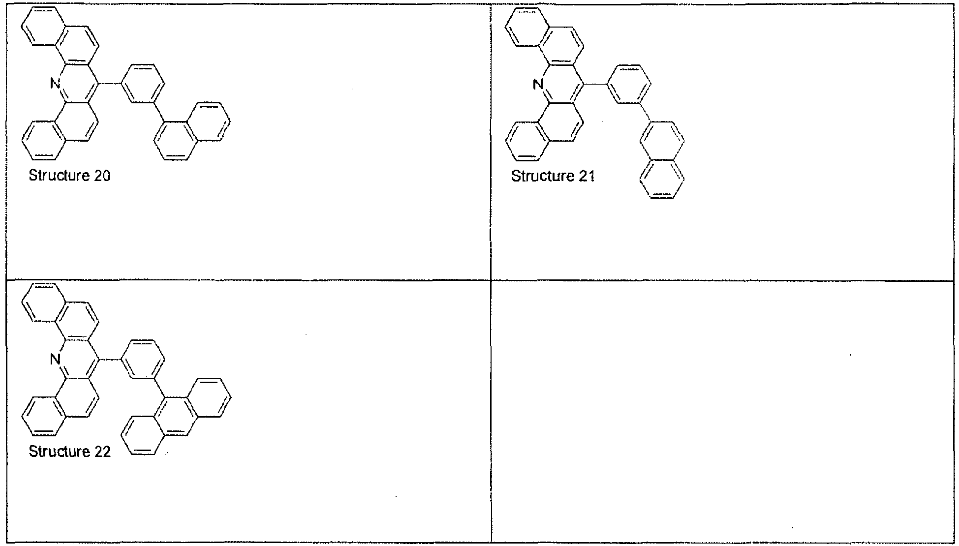
- As can be taken from above list, Ar and can be selected from a number of differently substituted or unsubstituted C6-C20-aryl or C5-C20-heteroaryl. Suitable substituents may be for example halogen, such as Br, Aryl, such as pyrene, or CF3.
- An organic n-dopant can be, for example, selected from the dopants as disclosed in
EP 2002492 A1 ,US 2007252140 orUS 2009212280 . - According to the invention is also an organic electronic device comprising an organic semiconducting material comprising at least one organic matrix material which is optionally doped with at least one dopant, wherein the matrix material comprises a compound according to formula (1).
- In a light-emitting diode the compounds can be used in electron transport layers, which might be optionally doped. The compounds can be also used in light-emitting diodes in interlayers such as hole blocking layers.
- According to the invention, the compounds are preferably used in the electron transport layer and not as main compound of the emitter layer, preferably they are not used in the emitter layer at all.
- According to the invention, especially a window semiconducting organic material is provided for the device that can be electrically doped achieving a high conductivity while it remains highly transparent in the visible spectra and has a high thermal stability.
- According to the invention, also an organic field-effect transistor can be provided comprising at least one compound according to formula (I) for use in a transport layer, in other words, in the semiconducting channel layer. An organic field effect transistor may also comprise at least one compound as disclosed as electronically inert buffer layer, when no charge is injected due to high potential barrier. An organic field effect transistor may also comprise at least one compound as disclosed as doped injection layer.
- The compounds used in this invention according to formula (I) can be used in OLEDs in electron transport layers as a neat layer, or as a doped layer in combination with a redox dopant. The compounds can also be used in mixture with other electron transport materials, with other hole transport materials or with other functional materials such as emitter dopants. The compounds can be used as hole blocking layers. Advantageous effects are seen over the prior art since the materials have a higher glass transition temperature compared to materials described in the prior art, such as in
DE 10 2007 012 794EP 07 400 033.2 - The use of the compounds according to formula (I) provides high thermal stability, especially due to high glass transition temperature, a good LUMO position for organic light-emitting devices, good dopability, conductivity and charge carrier mobility, high transparency, and easy synthesis. Further, preparation of these compounds can be conducted in a very cost-effective manner. Finally, it can be pointed out that the synthesis of such compounds offers a high flexibility to change independently the R and X, Ar1 or Ar2 groups which opens access to more complex compounds and therefore to different physical/chemical properties resulting in a fine tuning thereof.
- It was surprisingly found that especially the thermal stability of doped layers comprising a compound as disclosed can be significantly increased in the devices according to the present invention comprising matrix material. Especially, a glass transition temperature of over 100°C was achieved with the compounds shown in the examples. The combination of such a high glass temperature, the wide gap and the dopability make those compounds to have a high industrial relevance for use in organic electronic devices.
- The properties of the many different used materials can be described by the position of their highest occupied molecular orbital energy level (HOMO, synonym of ionization potential), and the lowest unoccupied molecular orbital energy level (LUMO, synonym of electron affinity).
- A method to determine the ionization potentials (IP) is the ultraviolet photo spectroscopy (UPS). It is usual to measure the ionization potential for solid state materials; however, it is also possible to measure the IP in the gas phase. Both values are differentiated by their solid state effects, which are, for example the polarization energy of the holes that are created during the photo ionization process. A typical value for the polarization energy is approximately 1 eV, but larger discrepancies of the values can also occur. The IP is related to beginning of the photoemission spectra in the region of the large kinetic energy of the photoelectrons, i.e. the energy of the most weakly bounded electrons. A related method to UPS, the inverted photo electron spectroscopy (IPES) can be used to determine the electron affinity (EA). However, this method is less common. Electrochemical measurements in solution are an alternative to the determination of solid state oxidation (Eox) and reduction (Ered) potential. An adequate method is for example the cyclo-voltammetry. Empiric methods for the extraction of the solid state ionization potentials are known from the literature. There are no known empiric equations for the conversion of reduction potentials into electron affinities. The reason for that is the difficulty of the determination of the electron affinity. Therefore, a simple rule is used very often: IP=4.8 eV+ e*Eox (vs. Ferrocen/Ferrocenium) and EA=4.8eV +e*Ered (vs. Ferrocen/Ferrocenium) respectively (see B.W. Andrade, Org. Electron. 6, 11 (2005) and Refs. 25-28 therein). Processes are known for the correction of the electrochemical potentials in the case other reference electrodes or other redox pairs are used (see A.J. Bard, L.R. Faulkner, "Electrochemical Methods: Fundamentals and Applications", S. 1-28, und S. 239-247, Wiley, 2. Ausgabe 2000). The information about the influence of the solution used can be found in N.G. Connelly et al., Chem. Rev. 96, 877 (1996). It is usual, even if not exactly correct to use the terms "energy of the HOMO" E(HOMO) and "energy of the LUMO" E(LUMO) respectively as synonyms for the ionization energy and electron affinity (Koopmans Theorem). It has to be taken in consideration, that the ionization potentials and the electron affinities are given in such a way that a larger value represents a stronger binding of a released or respectively of an absorbed electron. The energy scale of the molecular orbitals (HOMO, LUMO) is opposed to this. Therefore, in a rough approximation, is valid: IP=-E(HOMO) and EA=E(LUMO). The given potentials correspond to the solid-state potentials. Hole transport layers, including the respective blockers, mostly have HOMO in the range from -4.5 to -5.5 eV (below the vacuum level) and LUMO in the range of -1.5 eV to -3 eV. The HOMO levels of the emitter materials are in the range of -5 eV to -6.5 eV, and the LUMO in the range from -2 to -3 eV. Electron transport materials, including their respective blockers, have their HOMO in a range of -5.5 eV to -6.8 eV and LUMO in the range of -2.3 eV to -3.3 eV. The work function of the contact materials is around -4 to -5 eV for the anode and -3 to -4.5 eV for the cathode.
- The dopant donor is a molecule or a neutral radical or combination thereof with a HOMO energy level (ionization potential in solid state) more positive than -3.3 eV, preferably more positive than -2.8 eV, more preferably more positive than -2.6 eV. The HOMO of the donor can be estimated by cyclo-voltammetric measurements. An alternative way to measure the reduction potential is to measure the cation of the donor salt. The donor has to exhibit an oxidation potential that is smaller than or equal to -1.5 V vs Fc / Fc+ (Ferrum/Ferrocenium redox-pair), preferably smaller than -1.5 V, more preferably smaller than or equal to approximately -2.0 V, even more preferably smaller than or equal to -2.2 V. The molar mass of the donor is in a range between 100 and 2000 g/mol, preferably in a range from 200 and 1000 g / mol. The molar doping concentration is in the range of 1:10000 (dopant molecule : matrix molecule) and 1:2, preferably between 1:100 and 1:5, more preferably between 1:100 and 1:10. In individual cases doping concentrations larger than 1:2 are applied, e.g. if large conductivities are required. The donor can be created by a precursor during the layer forming (deposition) process or during a subsequent process of layer formation (see
DE 10307125.3 ). The above given value of the HOMO level of the donor refers to the resulting molecule or molecule radical. - A dopant acceptor is a molecule or a neutral radical or combination thereof with a LUMO level more negative than -4.5 eV, preferably more negative than -4.8 eV, more preferably more negative than -5.04 eV. The LUMO of the acceptor can be estimated by cyclo-voltammetric measurements. The acceptor has to exhibit a reduction potential that is larger than or equal to approximately -0.3 V vs Fc / Fc+ Ferrocene/Ferrocenium redox-pair), preferably larger than or equal to 0.0 V, preferably larger than or equal to 0.24 V. The molar mass of the aceptor is preferably in the range of 100 to 2000 g / mol, more preferably between 200 and 1000 g / mol, and even more preferably between 300 g/mol and 2000 g/mol. The molar doping concentration is in the range of 1:10000 (dopant molecule : matrix molecule) and 1:2, preferably between 1:100 and 1:5, more preferably between 1:100 and 1:10. In individual cases doping concentrations larger than 1:2 are applied, e.g. if large conductivities are required. The acceptor can be created by a precursor during the layer forming (deposition) process or during a subsequent process of layer formation. The above given value of the LUMO level of the acceptor refers to the resulting molecule or molecule radical.
- By using the term doping it is meant electrical doping as explained above. This doping can also be called redox-doping or charge transfer doping. It is known that the doping increases the density of charge carriers of a semiconducting matrix towards the charge carrier density of the undoped matrix. An electrically doped semiconductor layer also has an increased effective mobility in comparison with the undoped semiconductor matrix.
- The conductivity can be, for example, measured by the so-called 2-point or 4-point-method. Here, contacts of a conductive material, such as gold or indium-tin-oxide, are disposed on a substrate. Then, the thin film to be examined is applied onto the substrate, so that the contacts are covered by the thin film. After applying a voltage to the contacts the current is measured. From the geometry of the contacts and the thickness of the sample the resistance and therefore the conductivity of the thin film material can be determined. The four point or two point method give the same conductivity values for doped layers since the doped layers grant a good ohmic contact.
- The temperature stability can also be measured with that method in which the (undoped or doped) layer is heated stepwise, and after a waiting period, the conductivity is measured. The maximum temperature, which can be applied to the layer without loosing the desired semiconducting properties, is then the temperature just before the conductivity breaks down. For example, a doped layer can be heated on the substrate with two electrodes, as disclosed above, in steps of 1°C, wherein after each step there is a waiting period of 10 seconds. Then the conductivity is measured. The conductivity changes with temperature and breaks down abruptly at a particular temperature. The temperature stability is therefore the temperature up to which the conductivity does not break down abruptly. The measurement is performed in vacuum.
- Additional features and advantages of the invention can be taken from the following detailed description of preferred embodiments, together with the drawings as attached.
-
Fig. 1 shows a cross section of a typical exemplary small molecule OLED. - The organic electronic device of the present invention may be an organic light emitting diode.
Fig. 1 shows a typical layer structure of an organic light emitting diode. The layers are disposed on a substrate (10) in the following order: anode (11), p-doped hole transport layer (12), electron blocking layer (13), emission layer (14), hole blocking layer (15), n-electron transport layer (16), and cathode (17). Two or more layers can collapse into a smaller number of layers if properties can be combined. Inverted structure and multiple stacked OLEDs are also well known in the field. The emission layer is usually composed by an emitter matrix material and an emitter dopant; this layer can be also composed by several other layers to generate light with a broad spectrum combining several emitters, for example, to generate white light. -

- Of course, the R's in the above general synthesis scheme shall stand for R1-4 according to formula (I). Additionally, Ar shall in this general synthesis scheme be understood to stand for the moiety "Ar-R5" according to formual (I).
- Synthesis of

- First step: Synthesis of 2-benzylidene-3,4-dihydronaphthalen-1(2H)-one (1). All manipulations were carried out in air, without any further purification of commercial solvents/chemicals.

- A 250 mL flask was charged with tetralone (4g, 27.4 mmol) and benzaldehyde (3.88 g, 36.6 mmol). This was dissolved in warm tetrahydrofuran (15 mL), and to this yellow solution was slowly added a 4 wt % solution of KOH in methanol (125 mL). The reaction was stirred for 4 days at room temperature. The solvent was then removed under reduced pressure, and it was poured into 150mL of water and extracted with methylene chloride. The organic extract was dried over magnesium sulfate and filtered, and the solvent was removed at reduced pressure to afford 4.1g (64%) as white powder.
NMR: 1H NMR (500 MHz, CD2C12) δ 8.01 (dd, J = 64.7, 65.4, 2H), 7.71 - 6.92 (m, 8H), 3.39 - 2.64 (m, 4H). - Second step: Synthesis of 7-phenyl-5,6,8,9-tetrahydrodihenzo[c,h]acridine (2). All manipulations were carried out under argon.

- 1 (2.9g, 12.4 mmol) and tetralone (1.7g, 11.6 mmol) are introduced in a flask together with BF3.Et20 (1.8mL, 14.2 mmol). The mixture is stirred at 100°C for 4 hours and cooled to room temperature. Et20 was added (15mL) and the mixture is stirred for an additional hour. The precipitate is filtered and washed with Et20 (15 mL). This powder (1.9g) is then introduced at 0°C in a flask together with a ammonia-ethanol solution. The mixture was allowed to stir at room temperature for 6h, the solid was filtered and washed several times with ethanol. 1.4 g (34% yield) of a white powder was obtained.
- Third step: Synthesis of 7-phenyldibenzo[c,h]acridine (3). All manipulations were carried out under argon with dry solvents.

- 2 (1.55g, 4.31 mmol) was dissolved in 100 mL dioxane and 2,3-dichloro-5,6-dicyanobenzoquinone was added (6.88g, 30.3 mmol). The mixture was refluxed under argon for 2 days. The reaction mixture was then cooled to room temperature, poured in 300 mL saturated aqueous sodium carbonate solution and stirred at 65°C for 30min. The mixture was then cooled to room temperature, the precipitation was filtered and washed with water and methylene chloride. Yield: 1.1 g (72%).
1H NMR (500 MHz, CD2C12) δ 8.02 - 7.94 (m, 4H), 7.86 (dd, J = 1.2, 7.8, 2H), 7.71 (ddd, J = 5.9, 11.0, 25.9, 3H), 7.45 (dd, J = 7.3, 8.4, 4H), 7.20 (d, J = 8.7, 2H), 7.05 (ddd, J = 1.5, 7.0, 8.6, 2H). - Synthesis of

- First step: Synthesis of (E)-2-(4-bromobenzylidene)-3,4-dilhydronaphthalen-1(2H)-one (4). All manipulations were carried out in air, without any further purification of commercial solvents/chemicals.

- A 250 mL flask was charged with tetralone (3.22g, 22 mmol) and 4-bromobenzaldehyde (5.3g, 28.6 mmol). This was dissolved in warm tetrahydrofuran (12 mL), and to this yellow solution was slowly added a 4 wt % solution of KOH in methanol (100 mL). The reaction was stirred for 4 days at room temperature. The mixture was concentrated and reduced to approx 10% vol. The residue was filtered and washed with MTBE (3*50mL), dried, to afford a light yellow powder (6,61g, 96%).
- Second step: Synthesis of 7-(4-bromophenyl)-5,6,8,9-tetrahydrodibenzo[c,h]acridine (5). All manipulations were carried out under argon.
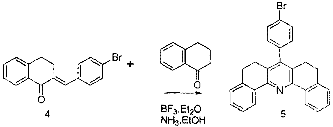
- 4 (6.54g, 20.9 mmol) and tetralone (2.93g, 20.0 mmol) are introduced in a flask together with BF3.Et20 (3mL, 23.7 mmol). The mixture is stirred at 100°C for 4 hours and cooled to room temperature. Et2O was added (25mL) and the mixture is stirred for an additional hour. The precipitate is filtered and washed with Et20 (20 mL). This powder (3.8g) is then introduced at 0°C in a flask together with an ammonia-ethanol solution. The mixture was allowed to stir at room temperature for 5h, the precipitate was filtered and washed several times with ethanol. 2.98 g (34% yield) of a white powder was obtained.
- Third step: Synthesis of 7-(4-bromopheny)dibenzo[c,h]acridine (6). All manipulations were carried out under argon with dry solvents.

- 2 (2.98g, 6.80 mmol) was dissolved in 190 mL dioxane and 2,3-dichloro-5,6-dicyanobenzoquinone was added (10.9g, 48 mmol). The mixture was refluxed under argon for 2 days. The reaction mixture was then cooled to room temperature, poured in 600 mL saturated aqueous sodium carbonate solution and stirred at 65°C for 30 min. The mixture was then cooled to room temperature, the precipitation was filtered and washed with water and dichloromethane.
Yield: 2g (68%).
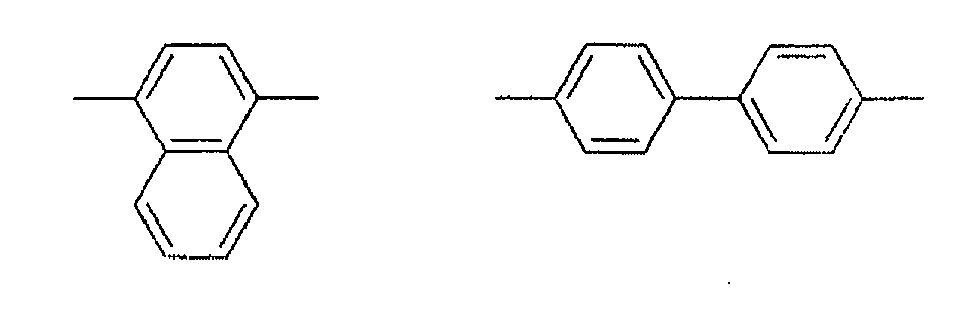
1H NMR (500 MHz, CD2Cl2) δ (ppm): 9.80 (d, J = 8.0, 2H), 8.00 - 7.68 (m, 10H), 7.53 (d, J = 9.2, 2H), 7.45 - 7.34 (m, 2H). - Fourth step: Synthesis of 4,4"-bis(dibenzo[c,h]acridin-7-yl)-1,1':4',1"-terphenyl (7). All manipulations were carried out in air, without any further purification of commercial solvents/chemicals.

- 6 (700mg, 1,61 mmol), 1,4-phenylenediboronic acid acid (146 mg, 0,88 mmol), Palladium tetrakis triphenylphoshine (186 mg, 0,16 mmol) and potassium carbonate (1,34g, 9,66 mmol) were introduced in a flask together with 17mL toluene, 8,8 mL ethanol and 2,6 mL distilled water. This mixture is stirred at 80°C during 24 hours before being filtered. The solid is then washed with hexane, water and some mL of chloroform before being dried.
Yield: 200 mg (20%). - Synthesis of

- First step: Synthesis of (E)-2-(3-bromobenzytidene)-3,4-dihydronaphthalen-1(2H)-one (8). All manipulations were carried out in air, without any further purification of commercial solvents/chemicals.
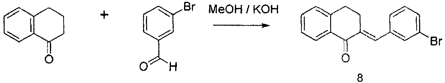
- A 250 mL flask was charged with tetralone (5.2g, 35.6 mmol) and 3-bromobenzaldehyde (8.51g, 56 mmol). This was dissolved in warm tetrahydrofuran (20 mL), and to this yellow solution was slowly added a 4 wt % solution of KOH in methanol (160 mL). The reaction was stirred for 4 days at room temperature. The mixture was concentrated and reduced to approx 10% vol. The residue was filtered and washed with MTBE (3*50mL), dried, to afford a light yellow powder (10.3g, 92%).
NMR: 1H NMR (500 MHz, CD2C12) δ 8.01 (dd, J = 64.7, 65.4, 2H), 7.71 - 6.92 (m, 8H), 3.39 - 2.64 (m, 4H). - Second step: Synthesis of 7-(3-bromophenyl)-5,6,8,9-tetrahydrodibenzo[c,b]acridine (9). All manipulations were carried out under argon.

- 4 (10.2g, 32.6 mmol) and tetralone (4.52g, 30.9 mmol) are introduced in a flask together with BF3.Et20 (4.7mL, 37.1 mmol). The mixture is stirred at 100°C for 4 hours and cooled to room temperature. Et2O was added (70 mL) and the mixture is stirred for an additional hour. The precipitate is filtered and washed with Et2O (20 mL). This powder (5.6g) is then introduced at 0°C in a flask together with an ammonia-ethanol solution. The mixture was allowed to stir at room temperature for 5h, the solid was filtered and washed several times with ethanol.
4.5 g (33% yield) of a white powder was obtained. - Third step: Synthesis of 7-(3-bromophenyl)dibenzo[c,h]acridine (10). All manipulations were carried out under argon and with dry solvents.

- 2 (4.49g, 10.2 mmol) was dissolved in 220 mL dioxane and 2,3-dichloro-5,6-dicyanobenzoquinone was added (14.3g, 63 mmol). The mixture was refluxed under argon for 2 days. The reaction mixture was then cooled to room temperature, poured in 700 mL saturated aqueous sodium carbonate solution and stirred at 65°C for 30min. The mixture was then cooled to room temperature; the precipitation was filtered and washed with water and dichloromethane.
Yield: 3.3g (74%).
1H NMR (500 MHz, CD2Cl2) δ (ppm): 9.80 (d, J = 8.1, 2H), 8.01 - 7.63 (m, 11 H), 7.61-7.40 (m, 4H). - Fourth step: Synthesis of 7-(3-(pyren-1-yl)phenyl)dibenzo[c,h]acridine (11). All manipulations were carried under argon.
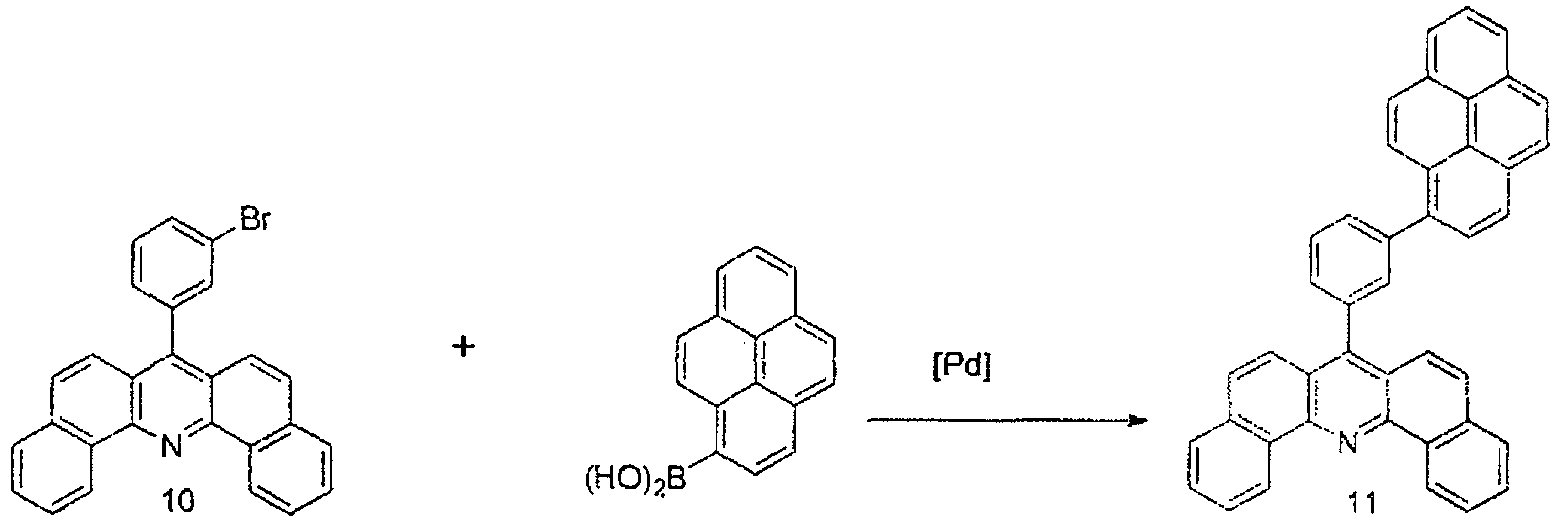
- 10 (700mg, 1,61 mmol), pyren-1-ylboronic acid (434 mg, 1,76 mmol), Palladium tetrakis triphenylphoshine (186 mg, 0,16 mmol) and potassium carbonate (1,34g, 9,66 mmol) were introduced in a flask together with 17mL toluene, 8,8 mL ethanol and 2,6 mL distilled water. This mixture is stirred at 80°C during 24 hours before being filtered. The solid is then washed with hexane, water and some mL of chloroform before being dried.
Yield: 392 mg (44%). - The conductivity of a doped layer consisting of material of structure 1 in table 1 doped with 5% of W(hpp)4 (Tetrakis (1,3,4,6,7,8-Hexahydro-2H-pyrimido[1,2-a] pyrimidinato) ditungsten (II)) was measured at room temperature and was 1.39x10⁻⁴ S/cm.
- The conductivity of a doped layer consisting of material of structure 18 in table 1 doped with 5% of W(hpp)4 was measured at room temperature and was 3x10⁻⁷ S/cm.
- The conductivity of a doped layer consisting of material of structure 3 in table 1 doped with 5% of W(hpp)4 was measured at room temperature and was 1.2x10⁻⁵ S/cm.
- The conductivity of a doped layer consisting of material of structure 2 in table 1 doped with 5% of W(hpp)4 was measured at room temperature and was 9.95x10⁻⁶ S/cm.
- The compounds from examples 1-3 were successfully employed as electron transport materials in OLEDs. An exemplary device structure is given below.
- An OLED was fabricated with the following procedure: A glass substrate coated with ITO (90 nm thick, pre-patterned) was cleaned in organic solvents in conventional ultra-sound. Afterwards the substrate was treated with ozone plasma for 5 minutes. After the cleaning, the substrate was transferred to vacuum. The organic layers were deposited in high vacuum (base pressure lower than 10-3 Pa) by conventional VTE (Vacuum thermal evaporation). The deposited area was defined by a shadow mask, keeping some area of the ITO surface free so that an electrical contact for the measurements could (later on) be established. The organic layer sequence over the ITO layer is: 50 nm thick NPD layer doped with F4TCNQ; 10 nm thick non-doped NPD layer, 20 nm blue emitter host layer doped with a fluorescent emitter; 10 nm ETL (structure 4), 60 nm ETL (structure 4) doped with W(hpp)4 (5% in weight). A 100 nm aluminum layer was deposited as cathode. The OLED reached 1000 cd/m2 at 3.59 V.
- Using the following material (14-(naphthalen-2-yl)dibenzo[a,j]acridine (structure 1b),

- An OLED was fabricated with the following procedure: A glass substrate coated with ITO (90 nm thick, pre-patterned) was cleaned in organic solvents in conventional ultra-sound. Afterwards the substrate was treated with ozone plasma for 5 minutes. After the cleaning, the substrate was transferred to vacuum. The organic layers were deposited in high vacuum (base pressure lower than 10-3 Pa) by conventional VTE (Vacuum thermal evaporation). The deposited area was defined by a shadow mask, keeping some area of the ITO surface free so that an electrical contact for the measurements could (later on) be established. The organic layer sequence over the ITO layer is: 50 nm thick NPD layer doped with F4TCNQ; 10 nm thick non-doped NPD layer, 20 nm blue emitter host layer doped with a fluorescent emitter; 10 nm ETL (structure Ib), 60 nm ETL (structure 1b) doped with W(hpp)4 (5% in weight). A 100 nm aluminum layer was deposited as cathode. The OLED reached 1000 cd/m2 at 4.25 V.

Claims (9)
- Organic electronic device comprising an organic semiconducting material comprising at least one compound according to the following formula (I):
 wherein R1-4 are independently selected from H, halogen, CN, substituted or unsubstituted C1-C20-alkyl or heteroalkyl, C6-C20-aryl or C5-C10-heteroaryl, C1-C20-alkoxy or C6-C20-aryloxy,Ar is selected from substituted or unsubstituted C6-C20-aryl or C5-C20-heteroaryl, andR5 is selected from substituted or unsubstituted C6-C20-aryl or C5-C20-heteroaryl, H or
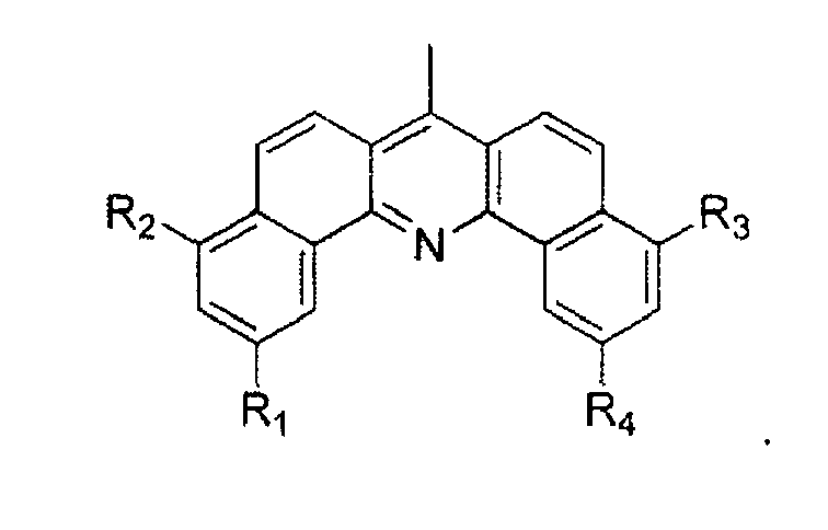
- Organic electronic device according to claim 1, wherein Ar and R1-4 are independently selected from C6-C20 aryl and C5-C20-heteroaryl.
- Organic electronic device according to claim 1 or 2, wherein R5 is H and combines with Ar to a moiety selected from


- Organic electronic device according to any of the preceding claims, wherein Ar is selected from


- Organic electronic device according to any of the preceding claims, wherein the device has a layered structure and at least one layer comprises at least one compound according to formula (I) as defined in claim 1.
- Organic electronic device according to any of the preceding claims, wherein the organic semiconducting material is doped by an n-dopant.
- Organic electronic device according to claim 6, wherein the organic semiconducting material is doped by an organic n-dopant which dopant has HOMO energy level which is more positive than -3.3 eV.
- Organic electronic device according to claim 1, wherein the device is an electronic, optoelectronic or electroluminescent device having an electronically functionally effect region, wherein the electronically effective region comprises at least one compound according to formula (I) as defined in claim 1.
- Organic electronic device according to any of the preceding claims, wherein the device is an organic light-emitting diode, a field-effect transistor, a sensor, a photodetector, an organic thin-film transistor, an organic integrated circuit, an organic light-emitting transistor, a light-emitting electrochemical cell or an organic laser diode.
Priority Applications (8)
| Application Number | Priority Date | Filing Date | Title |
|---|---|---|---|
| EP10165537.1A EP2395571B1 (en) | 2010-06-10 | 2010-06-10 | Organic electronic device comprising an organic semiconducting material |
| KR1020137000597A KR101866330B1 (en) | 2010-06-10 | 2011-06-08 | Electronic device comprising an organic semiconducting material |
| US13/699,532 US9040175B2 (en) | 2010-06-10 | 2011-06-08 | Electronic device comprising an organic semiconducting material |
| CN201180028541.XA CN102986050B (en) | 2010-06-10 | 2011-06-08 | Comprise the electronic device of organic semiconducting materials |
| PCT/EP2011/002807 WO2011154131A1 (en) | 2010-06-10 | 2011-06-08 | Electronic device comprising an organic semiconducting material |
| JP2013513579A JP6014027B2 (en) | 2010-06-10 | 2011-06-08 | Electronic devices containing organic semiconductor materials |
| US15/605,237 USRE48156E1 (en) | 2010-06-10 | 2011-06-08 | Electronic device comprising an organic semiconducting material |
| JP2016160075A JP6343311B2 (en) | 2010-06-10 | 2016-08-17 | Electronic devices containing organic semiconductor materials |
Applications Claiming Priority (1)
| Application Number | Priority Date | Filing Date | Title |
|---|---|---|---|
| EP10165537.1A EP2395571B1 (en) | 2010-06-10 | 2010-06-10 | Organic electronic device comprising an organic semiconducting material |
Publications (2)
| Publication Number | Publication Date |
|---|---|
| EP2395571A1 EP2395571A1 (en) | 2011-12-14 |
| EP2395571B1 true EP2395571B1 (en) | 2013-12-04 |
Family
ID=42470887
Family Applications (1)
| Application Number | Title | Priority Date | Filing Date |
|---|---|---|---|
| EP10165537.1A Active EP2395571B1 (en) | 2010-06-10 | 2010-06-10 | Organic electronic device comprising an organic semiconducting material |
Country Status (6)
| Country | Link |
|---|---|
| US (2) | USRE48156E1 (en) |
| EP (1) | EP2395571B1 (en) |
| JP (2) | JP6014027B2 (en) |
| KR (1) | KR101866330B1 (en) |
| CN (1) | CN102986050B (en) |
| WO (1) | WO2011154131A1 (en) |
Families Citing this family (54)
| Publication number | Priority date | Publication date | Assignee | Title |
|---|---|---|---|---|
| CN104067400B (en) | 2011-11-30 | 2018-02-27 | 诺瓦尔德股份有限公司 | Organic electronic device |
| TWI584513B (en) * | 2011-11-30 | 2017-05-21 | 諾瓦發光二極體有限公司 | Display |
| WO2013079678A1 (en) | 2011-11-30 | 2013-06-06 | Novaled Ag | Organic electronic device |
| CN103420910A (en) * | 2012-07-26 | 2013-12-04 | 烟台万润精细化工股份有限公司 | Electron-transport blue luminescent material and use thereof |
| DE102012109777A1 (en) | 2012-10-15 | 2014-04-17 | Heliatek Gmbh | Method for printing optoelectronic components with busbars |
| KR20140055452A (en) * | 2012-10-31 | 2014-05-09 | 삼성디스플레이 주식회사 | Organic light emitting device |
| KR20150014778A (en) * | 2013-07-30 | 2015-02-09 | 삼성디스플레이 주식회사 | Oganic light emitting device |
| CN103539737B (en) * | 2013-10-23 | 2017-03-08 | Tcl集团股份有限公司 | A kind of azepine phenanthro- fluorene kind derivative, preparation method and electroluminescent fluorescent luminescent device |
| KR102164046B1 (en) * | 2013-12-03 | 2020-10-12 | 덕산네오룩스 주식회사 | Compound for organic electronic element, organic electronic element using the same, and an electronic device thereof |
| ES2673573T3 (en) | 2013-12-23 | 2018-06-22 | Novaled Gmbh | Semiconductor material with doping N comprising a phosphine oxide matrix and a doping metal |
| KR102230191B1 (en) | 2014-05-14 | 2021-03-22 | 삼성디스플레이 주식회사 | Organic light-emitting device |
| KR102308903B1 (en) | 2014-06-17 | 2021-10-06 | 삼성디스플레이 주식회사 | Organic light emitting device |
| EP2963696A1 (en) | 2014-07-04 | 2016-01-06 | Novaled GmbH | Organic light-emitting diode (OLED) including an electron transport layer stack comprising different lithium compounds |
| EP2999019B1 (en) | 2014-09-19 | 2019-06-12 | Novaled GmbH | Organic light-emitting diode including an electron transport layer stack comprising different lithium compounds and elemental metal |
| EP3002801B1 (en) | 2014-09-30 | 2018-07-18 | Novaled GmbH | Organic electronic device |
| EP3002796A1 (en) | 2014-10-01 | 2016-04-06 | Novaled GmbH | Organic light-emitting diode including an electron transport layer comprising a three component blend of a matrix compound and two lithium compounds |
| KR101659292B1 (en) | 2014-11-28 | 2016-09-23 | (주)더블유에스 | Phosphoryl substituted Fluoranthene derivatives and organic electroluminescent device including the same |
| EP3035400B1 (en) | 2014-12-17 | 2019-10-23 | Novaled GmbH | Organic light-emitting diode comprising electron transport layers with different matrix compounds |
| EP3093288A1 (en) | 2015-05-12 | 2016-11-16 | Novaled GmbH | Organic light-emitting diode comprising different matrix compounds in the first and second electron transport layer |
| KR102364221B1 (en) | 2015-03-23 | 2022-02-18 | 삼성디스플레이 주식회사 | Condensed-cyclic compound and organic light emitting device comprising the same |
| US20180182960A1 (en) | 2015-06-23 | 2018-06-28 | Novaled Gmbh | Organic Light Emitting Device Comprising Polar Matrix and Metal Dopant |
| EP3109916B1 (en) | 2015-06-23 | 2021-08-25 | Novaled GmbH | Organic light emitting device comprising polar matrix, metal dopant and silver cathode |
| EP3109915B1 (en) | 2015-06-23 | 2021-07-21 | Novaled GmbH | Organic light emitting device comprising polar matrix and metal dopant |
| EP3109919B1 (en) | 2015-06-23 | 2021-06-23 | Novaled GmbH | N-doped semiconducting material comprising polar matrix and metal dopant |
| KR102491872B1 (en) | 2015-07-31 | 2023-01-27 | 삼성디스플레이 주식회사 | Condensed-cyclic compound and organic light-emitting device comprising the same |
| EP3133663B1 (en) | 2015-08-18 | 2022-06-15 | Novaled GmbH | Metal amides for use as hole injection layer for an organic light-emitting diode (oled) |
| EP3133664A1 (en) | 2015-08-18 | 2017-02-22 | Novaled GmbH | Triaryl amine thick layer doped with metal amides for use as hole injection layer for an organic light-emitting diode (oled) |
| EP3147958B1 (en) | 2015-09-28 | 2019-10-23 | Novaled GmbH | Organic electroluminescent devices comprising borane compounds |
| EP3147961A1 (en) * | 2015-09-28 | 2017-03-29 | Novaled GmbH | Organic electroluminescent device |
| KR102494453B1 (en) * | 2015-10-05 | 2023-02-02 | 삼성디스플레이 주식회사 | Organic electroluminescent device and display device including the same |
| KR102458684B1 (en) | 2015-10-08 | 2022-10-26 | 삼성디스플레이 주식회사 | Organic light emitting device |
| EP3171418B1 (en) | 2015-11-23 | 2024-12-11 | Novaled GmbH | Organic semiconductive layer comprising phosphine oxide compounds |
| EP3182478B1 (en) | 2015-12-18 | 2018-11-28 | Novaled GmbH | Electron injection layer for an organic light-emitting diode (oled) |
| EP3208861A1 (en) | 2016-02-19 | 2017-08-23 | Novaled GmbH | Electron transport layer comprising a matrix compound mixture for an organic light-emitting diode (oled) |
| KR102547685B1 (en) | 2016-02-22 | 2023-06-27 | 삼성디스플레이 주식회사 | Organic light emitting device |
| EP3232490B1 (en) | 2016-04-12 | 2021-03-17 | Novaled GmbH | Organic light emitting diode comprising an organic semiconductor layer |
| EP3252837B1 (en) | 2016-05-30 | 2021-05-05 | Novaled GmbH | Organic light emitting diode comprising an organic semiconductor layer |
| EP3252841B1 (en) | 2016-05-30 | 2026-04-01 | Novaled GmbH | Organic light emitting diode comprising an organic semiconductor layer |
| EP3291319B1 (en) | 2016-08-30 | 2019-01-23 | Novaled GmbH | Method for preparing an organic semiconductor layer |
| EP3312899B1 (en) | 2016-10-24 | 2021-04-07 | Novaled GmbH | Electron transport layer stack for an organic light-emitting diode |
| EP3312171B1 (en) * | 2016-10-24 | 2019-07-31 | Novaled GmbH | Compound for electronic device and electronic device and display device |
| EP3312895B1 (en) | 2016-10-24 | 2021-07-28 | Novaled GmbH | Organic semiconducting material comprising an electrical n-dopant and an electron transport matrix and electronic device comprising the semiconducting material |
| EP3312896B1 (en) | 2016-10-24 | 2021-03-31 | Novaled GmbH | Organic electroluminescent device comprising a redox-doped electron transport layer and an auxiliary electron transport layer |
| EP4164358A1 (en) | 2017-01-30 | 2023-04-12 | Novaled GmbH | Electroluminescent device comprising a defined layer arrangement comprising a light emitting layer, a hole transport layer and an electron transport layer |
| EP3583636B1 (en) * | 2017-02-20 | 2023-05-24 | Novaled GmbH | Electronic semiconducting device, method for preparing the electronic semiconducting device and compound |
| EP3369729B1 (en) * | 2017-03-02 | 2022-01-12 | Novaled GmbH | Fused 9-phenyl-acridine derivatives for use in an electronic device and display device |
| CN106816552B (en) * | 2017-03-03 | 2019-07-12 | 上海天马有机发光显示技术有限公司 | A kind of OLED display panel and the electronic equipment containing it |
| EP3406617B1 (en) | 2017-05-23 | 2021-03-24 | Novaled GmbH | Use of phosphine oxide compounds in a semiconducting layer comprised in an electronic device |
| EP3410510B1 (en) | 2017-06-02 | 2021-10-20 | Novaled GmbH | Organic electronic device and method for producing the organic electronic device |
| EP3556753B1 (en) * | 2018-04-18 | 2023-10-11 | Novaled GmbH | Compound and organic semiconducting layer, organic electronic device, display device and lighting device comprising the same |
| WO2019218276A1 (en) * | 2018-05-16 | 2019-11-21 | Merck Patent Gmbh | Organic semiconductors |
| KR102783339B1 (en) | 2018-06-12 | 2025-03-20 | 삼성디스플레이 주식회사 | Heterocyclic compound and organic light emitting device comprising the same |
| EP3653619A1 (en) * | 2018-11-16 | 2020-05-20 | Novaled GmbH | Compound, organic electronic device comprising the same, and display device and lighting device comprising the same |
| US20220216428A1 (en) | 2019-04-15 | 2022-07-07 | Novaled Gmbh | See addendum |
Family Cites Families (22)
| Publication number | Priority date | Publication date | Assignee | Title |
|---|---|---|---|---|
| US4356429A (en) | 1980-07-17 | 1982-10-26 | Eastman Kodak Company | Organic electroluminescent cell |
| US5093698A (en) | 1991-02-12 | 1992-03-03 | Kabushiki Kaisha Toshiba | Organic electroluminescent device |
| US6853083B1 (en) | 1995-03-24 | 2005-02-08 | Semiconductor Energy Laboratory Co., Ltd. | Thin film transfer, organic electroluminescence display device and manufacturing method of the same |
| JP3778649B2 (en) * | 1997-03-27 | 2006-05-24 | 三井化学株式会社 | Organic electroluminescence device |
| US7026643B2 (en) | 2001-05-04 | 2006-04-11 | International Business Machines Corporation | Organic n-channel semiconductor device of N,N' 3,4,9,10 perylene tetracarboxylic diimide |
| DE10207859A1 (en) | 2002-02-20 | 2003-09-04 | Univ Dresden Tech | Doped organic semiconductor material and process for its production |
| DE10215210B4 (en) | 2002-03-28 | 2006-07-13 | Novaled Gmbh | Transparent, thermally stable light-emitting component with organic layers |
| TW556446B (en) * | 2002-09-11 | 2003-10-01 | Opto Tech Corp | Organic light-emitting device and the manufacturing method thereof |
| DE102004010954A1 (en) | 2004-03-03 | 2005-10-06 | Novaled Gmbh | Use of a metal complex as an n-dopant for an organic semiconductive matrix material, organic semiconductor material and electronic component |
| WO2006015567A1 (en) * | 2004-08-13 | 2006-02-16 | Novaled Ag | Layer arrangement for a light-emitting component |
| DE502005002342D1 (en) | 2005-03-15 | 2008-02-07 | Novaled Ag | Light-emitting component |
| AT501688B1 (en) | 2005-04-08 | 2008-02-15 | Keba Ag | METHOD AND DEVICE FOR THE SAFE, UNLIMITED AND EXCLUSIVE ALLOCATION OF COMMAND POWER FOR A CONTROLLER TO A CONTROLLABLE TECHNICAL EQUIPMENT |
| US20060244370A1 (en) | 2005-05-02 | 2006-11-02 | Eastman Kodak Company | Light-emitting layer spacing in tandem OLED devices |
| DE602006001930D1 (en) | 2005-12-23 | 2008-09-04 | Novaled Ag | of organic layers |
| DE502006000749D1 (en) | 2006-03-21 | 2008-06-19 | Novaled Ag | Heterocyclic radical or diradical, their dimers, oligomers, polymers, dispiro compounds and polycycles, their use, organic semiconducting material and electronic component |
| EP1837927A1 (en) | 2006-03-22 | 2007-09-26 | Novaled AG | Use of heterocyclic radicals for doping of organic semiconductors |
| DE102006053644A1 (en) * | 2006-11-14 | 2008-06-12 | Siemens Ag | Novel highly conductive organic carrier transport material |
| US8795855B2 (en) | 2007-01-30 | 2014-08-05 | Global Oled Technology Llc | OLEDs having high efficiency and excellent lifetime |
| DE102007012794B3 (en) | 2007-03-16 | 2008-06-19 | Novaled Ag | Pyrido [3,2-h] quinazolines and / or their 5,6-dihydro derivatives, their method of preparation and doped organic semiconductor material containing them |
| JP5180498B2 (en) | 2007-03-20 | 2013-04-10 | 三洋電機株式会社 | Organic semiconductor material and organic transistor using the same |
| KR102189768B1 (en) | 2007-08-08 | 2020-12-14 | 유니버셜 디스플레이 코포레이션 | Single triphenylene chromophores in phosphorescent light emitting diodes |
| EP2072517B1 (en) | 2007-12-21 | 2015-01-21 | Novaled GmbH | Asymmetric phenanthrolins, method for their manufacture and doped organic semiconductor material containing them |
-
2010
- 2010-06-10 EP EP10165537.1A patent/EP2395571B1/en active Active
-
2011
- 2011-06-08 US US15/605,237 patent/USRE48156E1/en active Active
- 2011-06-08 WO PCT/EP2011/002807 patent/WO2011154131A1/en not_active Ceased
- 2011-06-08 CN CN201180028541.XA patent/CN102986050B/en active Active
- 2011-06-08 JP JP2013513579A patent/JP6014027B2/en active Active
- 2011-06-08 KR KR1020137000597A patent/KR101866330B1/en active Active
- 2011-06-08 US US13/699,532 patent/US9040175B2/en not_active Ceased
-
2016
- 2016-08-17 JP JP2016160075A patent/JP6343311B2/en active Active
Also Published As
| Publication number | Publication date |
|---|---|
| CN102986050A (en) | 2013-03-20 |
| CN102986050B (en) | 2015-10-07 |
| EP2395571A1 (en) | 2011-12-14 |
| US20130200341A1 (en) | 2013-08-08 |
| KR20130119413A (en) | 2013-10-31 |
| WO2011154131A1 (en) | 2011-12-15 |
| USRE48156E1 (en) | 2020-08-11 |
| JP6343311B2 (en) | 2018-06-13 |
| US9040175B2 (en) | 2015-05-26 |
| JP2017025072A (en) | 2017-02-02 |
| JP6014027B2 (en) | 2016-10-25 |
| KR101866330B1 (en) | 2018-06-11 |
| JP2013534047A (en) | 2013-08-29 |
Similar Documents
| Publication | Publication Date | Title |
|---|---|---|
| EP2395571B1 (en) | Organic electronic device comprising an organic semiconducting material | |
| EP2312663B1 (en) | Organic electronic device comprising an organic semiconducting material | |
| EP2246862A1 (en) | Organic electronic device comprising an organic semiconducting material | |
| EP2504871B1 (en) | Organic electronic device comprising an organic semiconducting material | |
| EP2194055B1 (en) | Bridged pyridoquinazoline or phenanthroline compounds and organic semiconducting material comprising that compound | |
| EP2463927B1 (en) | Material for organic electronic device and organic electronic device | |
| KR101995047B1 (en) | Organic electronic device | |
| EP2834321B1 (en) | Use of a semiconducting compound in an organic light emitting device | |
| KR101891224B1 (en) | Chemical compound for organic electronic device and organic electronic device | |
| CN102317406B (en) | Heterocyclic compounds and their applications in electronic and optoelectronic structural elements | |
| EP2811000B1 (en) | Organic electronic device | |
| TW201322522A (en) | monitor | |
| CN106459748B (en) | N-fluoroalkyl substituted dibromonaphthalimides and their use as semiconductors | |
| KR101715219B1 (en) | Quinoxaline compounds and semiconductor materials | |
| WO2010063609A2 (en) | Hole injection material |
Legal Events
| Date | Code | Title | Description |
|---|---|---|---|
| AK | Designated contracting states |
Kind code of ref document: A1 Designated state(s): AL AT BE BG CH CY CZ DE DK EE ES FI FR GB GR HR HU IE IS IT LI LT LU LV MC MK MT NL NO PL PT RO SE SI SK SM TR |
|
| AX | Request for extension of the european patent |
Extension state: BA ME RS |
|
| PUAI | Public reference made under article 153(3) epc to a published international application that has entered the european phase |
Free format text: ORIGINAL CODE: 0009012 |
|
| 17P | Request for examination filed |
Effective date: 20120606 |
|
| GRAP | Despatch of communication of intention to grant a patent |
Free format text: ORIGINAL CODE: EPIDOSNIGR1 |
|
| INTG | Intention to grant announced |
Effective date: 20130627 |
|
| GRAS | Grant fee paid |
Free format text: ORIGINAL CODE: EPIDOSNIGR3 |
|
| GRAA | (expected) grant |
Free format text: ORIGINAL CODE: 0009210 |
|
| AK | Designated contracting states |
Kind code of ref document: B1 Designated state(s): AL AT BE BG CH CY CZ DE DK EE ES FI FR GB GR HR HU IE IS IT LI LT LU LV MC MK MT NL NO PL PT RO SE SI SK SM TR |
|
| REG | Reference to a national code |
Ref country code: GB Ref legal event code: FG4D |
|
| RIN1 | Information on inventor provided before grant (corrected) |
Inventor name: PRETSCH, RAMONA Inventor name: FADHEL, OMRANE |
|
| REG | Reference to a national code |
Ref country code: CH Ref legal event code: EP |
|
| REG | Reference to a national code |
Ref country code: IE Ref legal event code: FG4D Ref country code: AT Ref legal event code: REF Ref document number: 643835 Country of ref document: AT Kind code of ref document: T Effective date: 20140115 |
|
| REG | Reference to a national code |
Ref country code: DE Ref legal event code: R096 Ref document number: 602010012143 Country of ref document: DE Effective date: 20140130 |
|
| REG | Reference to a national code |
Ref country code: NL Ref legal event code: VDEP Effective date: 20131204 |
|
| REG | Reference to a national code |
Ref country code: AT Ref legal event code: MK05 Ref document number: 643835 Country of ref document: AT Kind code of ref document: T Effective date: 20131204 |
|
| PG25 | Lapsed in a contracting state [announced via postgrant information from national office to epo] |
Ref country code: SE Free format text: LAPSE BECAUSE OF FAILURE TO SUBMIT A TRANSLATION OF THE DESCRIPTION OR TO PAY THE FEE WITHIN THE PRESCRIBED TIME-LIMIT Effective date: 20131204 Ref country code: FI Free format text: LAPSE BECAUSE OF FAILURE TO SUBMIT A TRANSLATION OF THE DESCRIPTION OR TO PAY THE FEE WITHIN THE PRESCRIBED TIME-LIMIT Effective date: 20131204 Ref country code: HR Free format text: LAPSE BECAUSE OF FAILURE TO SUBMIT A TRANSLATION OF THE DESCRIPTION OR TO PAY THE FEE WITHIN THE PRESCRIBED TIME-LIMIT Effective date: 20131204 Ref country code: NO Free format text: LAPSE BECAUSE OF FAILURE TO SUBMIT A TRANSLATION OF THE DESCRIPTION OR TO PAY THE FEE WITHIN THE PRESCRIBED TIME-LIMIT Effective date: 20140304 Ref country code: LT Free format text: LAPSE BECAUSE OF FAILURE TO SUBMIT A TRANSLATION OF THE DESCRIPTION OR TO PAY THE FEE WITHIN THE PRESCRIBED TIME-LIMIT Effective date: 20131204 Ref country code: NL Free format text: LAPSE BECAUSE OF FAILURE TO SUBMIT A TRANSLATION OF THE DESCRIPTION OR TO PAY THE FEE WITHIN THE PRESCRIBED TIME-LIMIT Effective date: 20131204 |
|
| REG | Reference to a national code |
Ref country code: LT Ref legal event code: MG4D |
|
| PG25 | Lapsed in a contracting state [announced via postgrant information from national office to epo] |
Ref country code: LV Free format text: LAPSE BECAUSE OF FAILURE TO SUBMIT A TRANSLATION OF THE DESCRIPTION OR TO PAY THE FEE WITHIN THE PRESCRIBED TIME-LIMIT Effective date: 20131204 Ref country code: CY Free format text: LAPSE BECAUSE OF FAILURE TO SUBMIT A TRANSLATION OF THE DESCRIPTION OR TO PAY THE FEE WITHIN THE PRESCRIBED TIME-LIMIT Effective date: 20131204 Ref country code: AT Free format text: LAPSE BECAUSE OF FAILURE TO SUBMIT A TRANSLATION OF THE DESCRIPTION OR TO PAY THE FEE WITHIN THE PRESCRIBED TIME-LIMIT Effective date: 20131204 |
|
| PG25 | Lapsed in a contracting state [announced via postgrant information from national office to epo] |
Ref country code: IS Free format text: LAPSE BECAUSE OF FAILURE TO SUBMIT A TRANSLATION OF THE DESCRIPTION OR TO PAY THE FEE WITHIN THE PRESCRIBED TIME-LIMIT Effective date: 20140404 Ref country code: EE Free format text: LAPSE BECAUSE OF FAILURE TO SUBMIT A TRANSLATION OF THE DESCRIPTION OR TO PAY THE FEE WITHIN THE PRESCRIBED TIME-LIMIT Effective date: 20131204 Ref country code: BE Free format text: LAPSE BECAUSE OF FAILURE TO SUBMIT A TRANSLATION OF THE DESCRIPTION OR TO PAY THE FEE WITHIN THE PRESCRIBED TIME-LIMIT Effective date: 20131204 |
|
| PG25 | Lapsed in a contracting state [announced via postgrant information from national office to epo] |
Ref country code: ES Free format text: LAPSE BECAUSE OF FAILURE TO SUBMIT A TRANSLATION OF THE DESCRIPTION OR TO PAY THE FEE WITHIN THE PRESCRIBED TIME-LIMIT Effective date: 20131204 Ref country code: RO Free format text: LAPSE BECAUSE OF FAILURE TO SUBMIT A TRANSLATION OF THE DESCRIPTION OR TO PAY THE FEE WITHIN THE PRESCRIBED TIME-LIMIT Effective date: 20131204 Ref country code: PT Free format text: LAPSE BECAUSE OF FAILURE TO SUBMIT A TRANSLATION OF THE DESCRIPTION OR TO PAY THE FEE WITHIN THE PRESCRIBED TIME-LIMIT Effective date: 20140404 Ref country code: PL Free format text: LAPSE BECAUSE OF FAILURE TO SUBMIT A TRANSLATION OF THE DESCRIPTION OR TO PAY THE FEE WITHIN THE PRESCRIBED TIME-LIMIT Effective date: 20131204 Ref country code: SK Free format text: LAPSE BECAUSE OF FAILURE TO SUBMIT A TRANSLATION OF THE DESCRIPTION OR TO PAY THE FEE WITHIN THE PRESCRIBED TIME-LIMIT Effective date: 20131204 Ref country code: CZ Free format text: LAPSE BECAUSE OF FAILURE TO SUBMIT A TRANSLATION OF THE DESCRIPTION OR TO PAY THE FEE WITHIN THE PRESCRIBED TIME-LIMIT Effective date: 20131204 |
|
| REG | Reference to a national code |
Ref country code: DE Ref legal event code: R097 Ref document number: 602010012143 Country of ref document: DE |
|
| PLBE | No opposition filed within time limit |
Free format text: ORIGINAL CODE: 0009261 |
|
| STAA | Information on the status of an ep patent application or granted ep patent |
Free format text: STATUS: NO OPPOSITION FILED WITHIN TIME LIMIT |
|
| PG25 | Lapsed in a contracting state [announced via postgrant information from national office to epo] |
Ref country code: DK Free format text: LAPSE BECAUSE OF FAILURE TO SUBMIT A TRANSLATION OF THE DESCRIPTION OR TO PAY THE FEE WITHIN THE PRESCRIBED TIME-LIMIT Effective date: 20131204 |
|
| 26N | No opposition filed |
Effective date: 20140905 |
|
| REG | Reference to a national code |
Ref country code: DE Ref legal event code: R097 Ref document number: 602010012143 Country of ref document: DE Effective date: 20140905 |
|
| PG25 | Lapsed in a contracting state [announced via postgrant information from national office to epo] |
Ref country code: LU Free format text: LAPSE BECAUSE OF FAILURE TO SUBMIT A TRANSLATION OF THE DESCRIPTION OR TO PAY THE FEE WITHIN THE PRESCRIBED TIME-LIMIT Effective date: 20140610 Ref country code: MC Free format text: LAPSE BECAUSE OF FAILURE TO SUBMIT A TRANSLATION OF THE DESCRIPTION OR TO PAY THE FEE WITHIN THE PRESCRIBED TIME-LIMIT Effective date: 20131204 |
|
| REG | Reference to a national code |
Ref country code: CH Ref legal event code: PL |
|
| PG25 | Lapsed in a contracting state [announced via postgrant information from national office to epo] |
Ref country code: SI Free format text: LAPSE BECAUSE OF FAILURE TO SUBMIT A TRANSLATION OF THE DESCRIPTION OR TO PAY THE FEE WITHIN THE PRESCRIBED TIME-LIMIT Effective date: 20131204 |
|
| REG | Reference to a national code |
Ref country code: IE Ref legal event code: MM4A |
|
| PG25 | Lapsed in a contracting state [announced via postgrant information from national office to epo] |
Ref country code: IE Free format text: LAPSE BECAUSE OF NON-PAYMENT OF DUE FEES Effective date: 20140610 Ref country code: CH Free format text: LAPSE BECAUSE OF NON-PAYMENT OF DUE FEES Effective date: 20140630 Ref country code: IT Free format text: LAPSE BECAUSE OF FAILURE TO SUBMIT A TRANSLATION OF THE DESCRIPTION OR TO PAY THE FEE WITHIN THE PRESCRIBED TIME-LIMIT Effective date: 20131204 Ref country code: LI Free format text: LAPSE BECAUSE OF NON-PAYMENT OF DUE FEES Effective date: 20140630 |
|
| PG25 | Lapsed in a contracting state [announced via postgrant information from national office to epo] |
Ref country code: MT Free format text: LAPSE BECAUSE OF FAILURE TO SUBMIT A TRANSLATION OF THE DESCRIPTION OR TO PAY THE FEE WITHIN THE PRESCRIBED TIME-LIMIT Effective date: 20131204 |
|
| PG25 | Lapsed in a contracting state [announced via postgrant information from national office to epo] |
Ref country code: SM Free format text: LAPSE BECAUSE OF FAILURE TO SUBMIT A TRANSLATION OF THE DESCRIPTION OR TO PAY THE FEE WITHIN THE PRESCRIBED TIME-LIMIT Effective date: 20131204 |
|
| REG | Reference to a national code |
Ref country code: FR Ref legal event code: PLFP Year of fee payment: 7 |
|
| PG25 | Lapsed in a contracting state [announced via postgrant information from national office to epo] |
Ref country code: BG Free format text: LAPSE BECAUSE OF FAILURE TO SUBMIT A TRANSLATION OF THE DESCRIPTION OR TO PAY THE FEE WITHIN THE PRESCRIBED TIME-LIMIT Effective date: 20131204 Ref country code: GR Free format text: LAPSE BECAUSE OF FAILURE TO SUBMIT A TRANSLATION OF THE DESCRIPTION OR TO PAY THE FEE WITHIN THE PRESCRIBED TIME-LIMIT Effective date: 20140305 |
|
| PG25 | Lapsed in a contracting state [announced via postgrant information from national office to epo] |
Ref country code: HU Free format text: LAPSE BECAUSE OF FAILURE TO SUBMIT A TRANSLATION OF THE DESCRIPTION OR TO PAY THE FEE WITHIN THE PRESCRIBED TIME-LIMIT; INVALID AB INITIO Effective date: 20100610 Ref country code: TR Free format text: LAPSE BECAUSE OF FAILURE TO SUBMIT A TRANSLATION OF THE DESCRIPTION OR TO PAY THE FEE WITHIN THE PRESCRIBED TIME-LIMIT Effective date: 20131204 |
|
| REG | Reference to a national code |
Ref country code: FR Ref legal event code: PLFP Year of fee payment: 8 |
|
| REG | Reference to a national code |
Ref country code: FR Ref legal event code: PLFP Year of fee payment: 9 |
|
| PG25 | Lapsed in a contracting state [announced via postgrant information from national office to epo] |
Ref country code: MK Free format text: LAPSE BECAUSE OF FAILURE TO SUBMIT A TRANSLATION OF THE DESCRIPTION OR TO PAY THE FEE WITHIN THE PRESCRIBED TIME-LIMIT Effective date: 20131204 |
|
| PG25 | Lapsed in a contracting state [announced via postgrant information from national office to epo] |
Ref country code: AL Free format text: LAPSE BECAUSE OF FAILURE TO SUBMIT A TRANSLATION OF THE DESCRIPTION OR TO PAY THE FEE WITHIN THE PRESCRIBED TIME-LIMIT Effective date: 20131204 |
|
| REG | Reference to a national code |
Ref country code: DE Ref legal event code: R079 Ref document number: 602010012143 Country of ref document: DE Free format text: PREVIOUS MAIN CLASS: H01L0051000000 Ipc: H10K0099000000 |
|
| REG | Reference to a national code |
Ref country code: FR Ref legal event code: PLFP Year of fee payment: 14 |
|
| P01 | Opt-out of the competence of the unified patent court (upc) registered |
Effective date: 20230515 |
|
| PGFP | Annual fee paid to national office [announced via postgrant information from national office to epo] |
Ref country code: DE Payment date: 20250402 Year of fee payment: 16 |
|
| PGFP | Annual fee paid to national office [announced via postgrant information from national office to epo] |
Ref country code: GB Payment date: 20250401 Year of fee payment: 16 |
|
| PGFP | Annual fee paid to national office [announced via postgrant information from national office to epo] |
Ref country code: FR Payment date: 20250401 Year of fee payment: 16 |