EP4164358A1 - Electroluminescent device comprising a defined layer arrangement comprising a light emitting layer, a hole transport layer and an electron transport layer - Google Patents
Electroluminescent device comprising a defined layer arrangement comprising a light emitting layer, a hole transport layer and an electron transport layer Download PDFInfo
- Publication number
- EP4164358A1 EP4164358A1 EP22211510.7A EP22211510A EP4164358A1 EP 4164358 A1 EP4164358 A1 EP 4164358A1 EP 22211510 A EP22211510 A EP 22211510A EP 4164358 A1 EP4164358 A1 EP 4164358A1
- Authority
- EP
- European Patent Office
- Prior art keywords
- layer
- transport layer
- electron transport
- group
- compound
- Prior art date
- Legal status (The legal status is an assumption and is not a legal conclusion. Google has not performed a legal analysis and makes no representation as to the accuracy of the status listed.)
- Pending
Links
- 230000005525 hole transport Effects 0.000 title claims abstract description 125
- 150000001875 compounds Chemical class 0.000 claims abstract description 187
- 239000011159 matrix material Substances 0.000 claims abstract description 103
- 125000003118 aryl group Chemical group 0.000 claims abstract description 100
- 239000002019 doping agent Substances 0.000 claims abstract description 53
- 125000000623 heterocyclic group Chemical group 0.000 claims abstract description 23
- 125000002837 carbocyclic group Chemical group 0.000 claims abstract description 13
- 239000000203 mixture Substances 0.000 claims abstract description 11
- 229910052751 metal Inorganic materials 0.000 claims description 61
- 239000002184 metal Chemical class 0.000 claims description 61
- -1 anthracene compound Chemical class 0.000 claims description 44
- 239000000126 substance Substances 0.000 claims description 35
- 150000002894 organic compounds Chemical class 0.000 claims description 34
- 125000004429 atom Chemical group 0.000 claims description 28
- 125000006749 (C6-C60) aryl group Chemical group 0.000 claims description 24
- 229910052744 lithium Inorganic materials 0.000 claims description 24
- 229910052708 sodium Inorganic materials 0.000 claims description 24
- 125000000217 alkyl group Chemical group 0.000 claims description 22
- 230000007935 neutral effect Effects 0.000 claims description 22
- 229910052769 Ytterbium Inorganic materials 0.000 claims description 20
- 125000001072 heteroaryl group Chemical group 0.000 claims description 18
- MWPLVEDNUUSJAV-UHFFFAOYSA-N anthracene Natural products C1=CC=CC2=CC3=CC=CC=C3C=C21 MWPLVEDNUUSJAV-UHFFFAOYSA-N 0.000 claims description 17
- 229910044991 metal oxide Inorganic materials 0.000 claims description 17
- 150000004706 metal oxides Chemical class 0.000 claims description 17
- 125000000008 (C1-C10) alkyl group Chemical group 0.000 claims description 15
- YLQBMQCUIZJEEH-UHFFFAOYSA-N Furan Chemical group C=1C=COC=1 YLQBMQCUIZJEEH-UHFFFAOYSA-N 0.000 claims description 15
- 229910052792 caesium Inorganic materials 0.000 claims description 15
- 229910052749 magnesium Inorganic materials 0.000 claims description 15
- 150000004696 coordination complex Chemical class 0.000 claims description 14
- 229910052698 phosphorus Inorganic materials 0.000 claims description 14
- 229910052717 sulfur Inorganic materials 0.000 claims description 14
- 229910052723 transition metal Inorganic materials 0.000 claims description 14
- 150000003624 transition metals Chemical class 0.000 claims description 14
- 125000006539 C12 alkyl group Chemical group [H]C([H])([H])C([H])([H])C([H])([H])C([H])([H])C([H])([H])C([H])([H])C([H])([H])C([H])([H])C([H])([H])C([H])([H])C([H])([H])C([H])([H])* 0.000 claims description 13
- 229910052760 oxygen Inorganic materials 0.000 claims description 13
- 150000002739 metals Chemical class 0.000 claims description 12
- 229910052712 strontium Inorganic materials 0.000 claims description 12
- 229910052783 alkali metal Inorganic materials 0.000 claims description 11
- MPQXHAGKBWFSNV-UHFFFAOYSA-N oxidophosphanium Chemical group [PH3]=O MPQXHAGKBWFSNV-UHFFFAOYSA-N 0.000 claims description 11
- 229910052700 potassium Inorganic materials 0.000 claims description 11
- 229910052791 calcium Inorganic materials 0.000 claims description 9
- 229910052757 nitrogen Inorganic materials 0.000 claims description 9
- 230000003647 oxidation Effects 0.000 claims description 9
- 238000007254 oxidation reaction Methods 0.000 claims description 9
- 229910052701 rubidium Inorganic materials 0.000 claims description 9
- 150000003839 salts Chemical class 0.000 claims description 9
- 150000001340 alkali metals Chemical class 0.000 claims description 8
- 238000000034 method Methods 0.000 claims description 8
- 125000004437 phosphorous atom Chemical group 0.000 claims description 8
- 229910052693 Europium Inorganic materials 0.000 claims description 7
- 229910052784 alkaline earth metal Inorganic materials 0.000 claims description 7
- 150000001342 alkaline earth metals Chemical class 0.000 claims description 7
- KTWOOEGAPBSYNW-UHFFFAOYSA-N ferrocene Chemical compound [Fe+2].C=1C=C[CH-]C=1.C=1C=C[CH-]C=1 KTWOOEGAPBSYNW-UHFFFAOYSA-N 0.000 claims description 7
- 229910052761 rare earth metal Inorganic materials 0.000 claims description 7
- 150000002910 rare earth metals Chemical class 0.000 claims description 7
- 229910052711 selenium Inorganic materials 0.000 claims description 7
- BOXSCYUXSBYGRD-UHFFFAOYSA-N cyclopenta-1,3-diene;iron(3+) Chemical compound [Fe+3].C=1C=C[CH-]C=1.C=1C=C[CH-]C=1 BOXSCYUXSBYGRD-UHFFFAOYSA-N 0.000 claims description 6
- TXCDCPKCNAJMEE-UHFFFAOYSA-N dibenzofuran Chemical compound C1=CC=C2C3=CC=CC=C3OC2=C1 TXCDCPKCNAJMEE-UHFFFAOYSA-N 0.000 claims description 6
- 125000005842 heteroatom Chemical group 0.000 claims description 5
- 125000002347 octyl group Chemical group [H]C([*])([H])C([H])([H])C([H])([H])C([H])([H])C([H])([H])C([H])([H])C([H])([H])C([H])([H])[H] 0.000 claims description 5
- GBMBLXQWVALWHS-UHFFFAOYSA-N 1h-phosphepine Chemical group P1C=CC=CC=C1 GBMBLXQWVALWHS-UHFFFAOYSA-N 0.000 claims description 4
- 125000002915 carbonyl group Chemical group [*:2]C([*:1])=O 0.000 claims description 4
- 125000006575 electron-withdrawing group Chemical group 0.000 claims description 4
- 229910052736 halogen Inorganic materials 0.000 claims description 4
- 150000002367 halogens Chemical class 0.000 claims description 4
- 125000002560 nitrile group Chemical group 0.000 claims description 4
- 125000000449 nitro group Chemical group [O-][N+](*)=O 0.000 claims description 4
- 125000005010 perfluoroalkyl group Chemical group 0.000 claims description 4
- 230000000737 periodic effect Effects 0.000 claims description 4
- 125000000472 sulfonyl group Chemical group *S(*)(=O)=O 0.000 claims description 4
- DXBHBZVCASKNBY-UHFFFAOYSA-N 1,2-Benz(a)anthracene Chemical compound C1=CC=C2C3=CC4=CC=CC=C4C=C3C=CC2=C1 DXBHBZVCASKNBY-UHFFFAOYSA-N 0.000 claims description 3
- YTPLMLYBLZKORZ-UHFFFAOYSA-N Thiophene Chemical group C=1C=CSC=1 YTPLMLYBLZKORZ-UHFFFAOYSA-N 0.000 claims description 3
- RFRXIWQYSOIBDI-UHFFFAOYSA-N benzarone Chemical compound CCC=1OC2=CC=CC=C2C=1C(=O)C1=CC=C(O)C=C1 RFRXIWQYSOIBDI-UHFFFAOYSA-N 0.000 claims description 3
- 238000010561 standard procedure Methods 0.000 claims description 3
- 125000001424 substituent group Chemical group 0.000 claims description 3
- DGEZNRSVGBDHLK-UHFFFAOYSA-N [1,10]phenanthroline Chemical group C1=CN=C2C3=NC=CC=C3C=CC2=C1 DGEZNRSVGBDHLK-UHFFFAOYSA-N 0.000 claims 1
- 239000010410 layer Substances 0.000 description 332
- 238000002347 injection Methods 0.000 description 40
- 239000007924 injection Substances 0.000 description 40
- 239000000463 material Substances 0.000 description 30
- 239000011734 sodium Substances 0.000 description 21
- WYURNTSHIVDZCO-UHFFFAOYSA-N Tetrahydrofuran Chemical compound C1CCOC1 WYURNTSHIVDZCO-UHFFFAOYSA-N 0.000 description 14
- 239000011777 magnesium Substances 0.000 description 14
- 150000003254 radicals Chemical class 0.000 description 14
- 239000007789 gas Substances 0.000 description 13
- 238000004770 highest occupied molecular orbital Methods 0.000 description 10
- 239000012044 organic layer Substances 0.000 description 10
- 239000011575 calcium Substances 0.000 description 9
- 238000002484 cyclic voltammetry Methods 0.000 description 9
- 239000000758 substrate Substances 0.000 description 9
- 238000000151 deposition Methods 0.000 description 7
- KTSGGWMVDAECFK-UHFFFAOYSA-N 2,4,7,9-tetraphenyl-1,10-phenanthroline Chemical compound C1=CC=CC=C1C1=CC(C=2C=CC=CC=2)=C(C=CC=2C3=NC(=CC=2C=2C=CC=CC=2)C=2C=CC=CC=2)C3=N1 KTSGGWMVDAECFK-UHFFFAOYSA-N 0.000 description 6
- BQCADISMDOOEFD-UHFFFAOYSA-N Silver Chemical compound [Ag] BQCADISMDOOEFD-UHFFFAOYSA-N 0.000 description 6
- 239000011248 coating agent Substances 0.000 description 6
- 238000000576 coating method Methods 0.000 description 6
- 230000008021 deposition Effects 0.000 description 6
- 238000002207 thermal evaporation Methods 0.000 description 6
- 238000001771 vacuum deposition Methods 0.000 description 6
- ACBBFJIUCSTQSN-UHFFFAOYSA-N 1-[4-(3-diphenylphosphorylphenyl)phenyl]pyrene Chemical compound C1(=CC=CC=C1)P(C=1C=C(C=CC=1)C1=CC=C(C=C1)C1=CC=C2C=CC3=CC=CC4=CC=C1C2=C34)(C1=CC=CC=C1)=O ACBBFJIUCSTQSN-UHFFFAOYSA-N 0.000 description 5
- 230000000903 blocking effect Effects 0.000 description 5
- 239000000872 buffer Substances 0.000 description 5
- 229910052709 silver Inorganic materials 0.000 description 5
- WMZCREDANYEXRT-UHFFFAOYSA-N 1-[phenyl(pyren-1-yl)phosphoryl]pyrene Chemical compound C=1C=C(C2=C34)C=CC3=CC=CC4=CC=C2C=1P(C=1C2=CC=C3C=CC=C4C=CC(C2=C43)=CC=1)(=O)C1=CC=CC=C1 WMZCREDANYEXRT-UHFFFAOYSA-N 0.000 description 4
- AGRXWRGWMHZTHN-UHFFFAOYSA-N 4,7-diphenyl-2,9-bis(4-phenylphenyl)-1,10-phenanthroline Chemical compound C1=CC=CC=C1C1=CC=C(C=2N=C3C4=NC(=CC(=C4C=CC3=C(C=3C=CC=CC=3)C=2)C=2C=CC=CC=2)C=2C=CC(=CC=2)C=2C=CC=CC=2)C=C1 AGRXWRGWMHZTHN-UHFFFAOYSA-N 0.000 description 4
- 239000010405 anode material Substances 0.000 description 4
- 229910052799 carbon Inorganic materials 0.000 description 4
- 150000001768 cations Chemical class 0.000 description 4
- 125000004093 cyano group Chemical group *C#N 0.000 description 4
- 238000000295 emission spectrum Methods 0.000 description 4
- 230000001976 improved effect Effects 0.000 description 4
- 238000005259 measurement Methods 0.000 description 4
- 230000002093 peripheral effect Effects 0.000 description 4
- 150000004059 quinone derivatives Chemical class 0.000 description 4
- 239000004332 silver Substances 0.000 description 4
- 238000004528 spin coating Methods 0.000 description 4
- WBTZHYVXBIBLSU-UHFFFAOYSA-N 1-[3-[phenyl-(3-pyren-1-ylphenyl)phosphoryl]phenyl]pyrene Chemical compound O=P(c1ccccc1)(c1cccc(c1)-c1ccc2ccc3cccc4ccc1c2c34)c1cccc(c1)-c1ccc2ccc3cccc4ccc1c2c34 WBTZHYVXBIBLSU-UHFFFAOYSA-N 0.000 description 3
- MTJSYJGZDGFBQI-UHFFFAOYSA-N 13-(3-diphenylphosphorylphenyl)-2-azapentacyclo[12.8.0.03,12.04,9.017,22]docosa-1,3(12),4,6,8,10,13,15,17,19,21-undecaene Chemical compound C=1C=CC=CC=1P(C=1C=C(C=CC=1)C=1C2=C(C3=CC=CC=C3C=C2)N=C2C3=CC=CC=C3C=CC2=1)(=O)C1=CC=CC=C1 MTJSYJGZDGFBQI-UHFFFAOYSA-N 0.000 description 3
- GTVPDQGQEQCBRB-UHFFFAOYSA-N 13-[3-(4-diphenylphosphorylphenyl)phenyl]-2-azapentacyclo[12.8.0.03,12.04,9.017,22]docosa-1,3(12),4,6,8,10,13,15,17,19,21-undecaene Chemical compound C1=CC=CC=2C=CC=3C(=C4C=CC5=C(C4=NC=3C=21)C=CC=C5)C=1C=C(C=CC=1)C1=CC=C(C=C1)P(C1=CC=CC=C1)(C1=CC=CC=C1)=O GTVPDQGQEQCBRB-UHFFFAOYSA-N 0.000 description 3
- WDAQHTUHHZEGIO-UHFFFAOYSA-N 2-(3-diphenylphosphorylphenyl)-9,10-dinaphthalen-2-ylanthracene Chemical compound O=P(c1ccccc1)(c1ccccc1)c1cccc(c1)-c1ccc2c(-c3ccc4ccccc4c3)c3ccccc3c(-c3ccc4ccccc4c3)c2c1 WDAQHTUHHZEGIO-UHFFFAOYSA-N 0.000 description 3
- IXHWGNYCZPISET-UHFFFAOYSA-N 2-[4-(dicyanomethylidene)-2,3,5,6-tetrafluorocyclohexa-2,5-dien-1-ylidene]propanedinitrile Chemical compound FC1=C(F)C(=C(C#N)C#N)C(F)=C(F)C1=C(C#N)C#N IXHWGNYCZPISET-UHFFFAOYSA-N 0.000 description 3
- UICMBMCOVLMLIE-UHFFFAOYSA-N 2-[4-[4-(4,6-diphenyl-1,3,5-triazin-2-yl)phenyl]phenyl]-4,6-diphenyl-1,3,5-triazine Chemical group C1=CC=CC=C1C1=NC(C=2C=CC=CC=2)=NC(C=2C=CC(=CC=2)C=2C=CC(=CC=2)C=2N=C(N=C(N=2)C=2C=CC=CC=2)C=2C=CC=CC=2)=N1 UICMBMCOVLMLIE-UHFFFAOYSA-N 0.000 description 3
- CWSJTTXLYKIKHI-UHFFFAOYSA-N 2-diphenylphosphoryl-5-pyren-1-ylpyridine Chemical compound O=P(c1ccccc1)(c1ccccc1)c1ccc(cn1)-c1ccc2ccc3cccc4ccc1c2c34 CWSJTTXLYKIKHI-UHFFFAOYSA-N 0.000 description 3
- YGNHBARMWARKKZ-UHFFFAOYSA-N C1=CC=CC2=CC3=CC=CC=C3C(=C12)C1=CC=C(C=C1)P(C1=CC=CC=C1)(C1=CC=C(C=C1)C=1C2=CC=CC=C2C=C2C=CC=CC=12)=O Chemical compound C1=CC=CC2=CC3=CC=CC=C3C(=C12)C1=CC=C(C=C1)P(C1=CC=CC=C1)(C1=CC=C(C=C1)C=1C2=CC=CC=C2C=C2C=CC=CC=12)=O YGNHBARMWARKKZ-UHFFFAOYSA-N 0.000 description 3
- JPOANEPELSEQOU-UHFFFAOYSA-J C1=CN=C2C(O[Zr](OC=3C4=NC=CN=C4C=CC=3)(OC=3C4=NC=CN=C4C=CC=3)OC=3C4=NC=CN=C4C=CC=3)=CC=CC2=N1 Chemical compound C1=CN=C2C(O[Zr](OC=3C4=NC=CN=C4C=CC=3)(OC=3C4=NC=CN=C4C=CC=3)OC=3C4=NC=CN=C4C=CC=3)=CC=CC2=N1 JPOANEPELSEQOU-UHFFFAOYSA-J 0.000 description 3
- 229910045601 alloy Inorganic materials 0.000 description 3
- 239000000956 alloy Substances 0.000 description 3
- 125000006615 aromatic heterocyclic group Chemical group 0.000 description 3
- 230000015572 biosynthetic process Effects 0.000 description 3
- 125000004432 carbon atom Chemical group C* 0.000 description 3
- 239000011521 glass Substances 0.000 description 3
- 239000010931 gold Substances 0.000 description 3
- 229910052739 hydrogen Inorganic materials 0.000 description 3
- 238000004519 manufacturing process Methods 0.000 description 3
- 229910001092 metal group alloy Inorganic materials 0.000 description 3
- 229910000476 molybdenum oxide Inorganic materials 0.000 description 3
- QGLKJKCYBOYXKC-UHFFFAOYSA-N nonaoxidotritungsten Chemical compound O=[W]1(=O)O[W](=O)(=O)O[W](=O)(=O)O1 QGLKJKCYBOYXKC-UHFFFAOYSA-N 0.000 description 3
- 150000002902 organometallic compounds Chemical class 0.000 description 3
- PQQKPALAQIIWST-UHFFFAOYSA-N oxomolybdenum Chemical compound [Mo]=O PQQKPALAQIIWST-UHFFFAOYSA-N 0.000 description 3
- BASFCYQUMIYNBI-UHFFFAOYSA-N platinum Chemical compound [Pt] BASFCYQUMIYNBI-UHFFFAOYSA-N 0.000 description 3
- 230000002829 reductive effect Effects 0.000 description 3
- 239000000243 solution Substances 0.000 description 3
- XOLBLPGZBRYERU-UHFFFAOYSA-N tin dioxide Chemical compound O=[Sn]=O XOLBLPGZBRYERU-UHFFFAOYSA-N 0.000 description 3
- FIQMHBFVRAXMOP-UHFFFAOYSA-N triphenylphosphane oxide Chemical compound C=1C=CC=CC=1P(C=1C=CC=CC=1)(=O)C1=CC=CC=C1 FIQMHBFVRAXMOP-UHFFFAOYSA-N 0.000 description 3
- 229910001930 tungsten oxide Inorganic materials 0.000 description 3
- ZYIASNRIQAVFSO-UHFFFAOYSA-N 13-(4-phenylphenyl)-2-azapentacyclo[12.8.0.03,12.04,9.017,22]docosa-1,3(12),4,6,8,10,13,15,17,19,21-undecaene Chemical compound C1=CC=CC=C1C1=CC=C(C=2C3=C(C4=CC=CC=C4C=C3)N=C3C4=CC=CC=C4C=CC3=2)C=C1 ZYIASNRIQAVFSO-UHFFFAOYSA-N 0.000 description 2
- CHQXFBMXJZYHHW-UHFFFAOYSA-N 13-naphthalen-2-yl-2-azapentacyclo[12.8.0.03,12.04,9.017,22]docosa-1,3(12),4,6,8,10,13,15,17,19,21-undecaene Chemical compound C1=CC2=CC=CC=C2C2=C1C(C1=CC3=CC=CC=C3C=C1)=C(C=CC=1C3=CC=CC=1)C3=N2 CHQXFBMXJZYHHW-UHFFFAOYSA-N 0.000 description 2
- CENPSTJGQOQKKW-UHFFFAOYSA-N 2,4,6-tris(4-phenylphenyl)-1,3,5-triazine Chemical compound C1=CC=CC=C1C1=CC=C(C=2N=C(N=C(N=2)C=2C=CC(=CC=2)C=2C=CC=CC=2)C=2C=CC(=CC=2)C=2C=CC=CC=2)C=C1 CENPSTJGQOQKKW-UHFFFAOYSA-N 0.000 description 2
- AHCKQUCVVVLQIV-UHFFFAOYSA-N 2,9-bis(4-methylphenyl)-4,7-diphenyl-1,10-phenanthroline Chemical compound C1=CC(C)=CC=C1C1=CC(C=2C=CC=CC=2)=C(C=CC=2C3=NC(=CC=2C=2C=CC=CC=2)C=2C=CC(C)=CC=2)C3=N1 AHCKQUCVVVLQIV-UHFFFAOYSA-N 0.000 description 2
- VOZBMWWMIQGZGM-UHFFFAOYSA-N 2-[4-(9,10-dinaphthalen-2-ylanthracen-2-yl)phenyl]-1-phenylbenzimidazole Chemical compound C1=CC=CC=C1N1C2=CC=CC=C2N=C1C1=CC=C(C=2C=C3C(C=4C=C5C=CC=CC5=CC=4)=C4C=CC=CC4=C(C=4C=C5C=CC=CC5=CC=4)C3=CC=2)C=C1 VOZBMWWMIQGZGM-UHFFFAOYSA-N 0.000 description 2
- BRAHEWAYJMQHNE-UHFFFAOYSA-N 2-ethyl-1-[4-[10-(4-phenylphenyl)anthracen-9-yl]phenyl]benzimidazole Chemical compound CCC1=NC2=CC=CC=C2N1C(C=C1)=CC=C1C(C1=CC=CC=C11)=C2C=CC=CC2=C1C(C=C1)=CC=C1C1=CC=CC=C1 BRAHEWAYJMQHNE-UHFFFAOYSA-N 0.000 description 2
- GYUPAYHPAZQUMB-UHFFFAOYSA-N 2-phenyl-9-[3-(9-phenyl-1,10-phenanthrolin-2-yl)phenyl]-1,10-phenanthroline Chemical compound C1=CC=CC=C1C1=CC=C(C=CC=2C3=NC(=CC=2)C=2C=C(C=CC=2)C=2N=C4C5=NC(=CC=C5C=CC4=CC=2)C=2C=CC=CC=2)C3=N1 GYUPAYHPAZQUMB-UHFFFAOYSA-N 0.000 description 2
- FYHIADQICQJZMV-UHFFFAOYSA-N 3,8-bis(6-phenylpyridin-2-yl)-1,10-phenanthroline Chemical compound C1(=CC=CC=C1)C1=CC=CC(=N1)C=1C=NC2=C3N=CC(=CC3=CC=C2C=1)C1=NC(=CC=C1)C1=CC=CC=C1 FYHIADQICQJZMV-UHFFFAOYSA-N 0.000 description 2
- DEECBJZHFWCFGJ-UHFFFAOYSA-N 3-(9-phenylcarbazol-3-yl)-9-(4-phenylquinazolin-2-yl)carbazole Chemical compound C1=CC=CC=C1C1=NC(N2C3=CC=C(C=C3C3=CC=CC=C32)C=2C=C3C4=CC=CC=C4N(C=4C=CC=CC=4)C3=CC=2)=NC2=CC=CC=C12 DEECBJZHFWCFGJ-UHFFFAOYSA-N 0.000 description 2
- UWYXJMMTYQBEEX-UHFFFAOYSA-N 3-[4-(4,6-dinaphthalen-2-yl-1,3,5-triazin-2-yl)phenyl]quinoline Chemical compound C1=CC=CC2=CC(C3=CC=C(C=C3)C=3N=C(N=C(N=3)C=3C=C4C=CC=CC4=CC=3)C3=CC4=CC=CC=C4C=C3)=CN=C21 UWYXJMMTYQBEEX-UHFFFAOYSA-N 0.000 description 2
- HAKTVPNPXHBHCP-UHFFFAOYSA-N 3-[4-[3-(10-phenylanthracen-9-yl)phenyl]phenyl]quinoline Chemical compound C1(=CC=CC=C1)C1=C2C=CC=CC2=C(C2=CC=CC=C12)C=1C=C(C=CC=1)C1=CC=C(C=C1)C=1C=NC2=CC=CC=C2C=1 HAKTVPNPXHBHCP-UHFFFAOYSA-N 0.000 description 2
- SQCXYLOBUMNYOK-UHFFFAOYSA-N 4-naphthalen-1-yl-2,7,9-triphenylpyrido[3,2-h]quinazoline Chemical compound C1=CC=CC=C1C1=CC(C=2C=CC=CC=2)=C(C=CC=2C3=NC(=NC=2C=2C4=CC=CC=C4C=CC=2)C=2C=CC=CC=2)C3=N1 SQCXYLOBUMNYOK-UHFFFAOYSA-N 0.000 description 2
- OUUQIUKIMMOUPJ-UHFFFAOYSA-N 4-naphthalen-2-yl-2-(4-quinolin-3-ylphenyl)benzo[h]quinazoline Chemical compound C1=C(C=CC2=CC=CC=C12)C1=NC(=NC2=C3C(=CC=C12)C=CC=C3)C1=CC=C(C=C1)C=1C=NC2=CC=CC=C2C=1 OUUQIUKIMMOUPJ-UHFFFAOYSA-N 0.000 description 2
- XKRFYHLGVUSROY-UHFFFAOYSA-N Argon Chemical compound [Ar] XKRFYHLGVUSROY-UHFFFAOYSA-N 0.000 description 2
- RKASPCVDTJRRJQ-UHFFFAOYSA-N C1(C=2C=CC=CC=2)=NC(C2=CC=CC=C2)=NC(=N1)C1=CC(C2=C3C(=C4C(C=CC=C4)=C2)C=CC=C3)=CC(C2=CN=C(C=C2)C2=NC(C)=CC=C2)=C1 Chemical compound C1(C=2C=CC=CC=2)=NC(C2=CC=CC=C2)=NC(=N1)C1=CC(C2=C3C(=C4C(C=CC=C4)=C2)C=CC=C3)=CC(C2=CN=C(C=C2)C2=NC(C)=CC=C2)=C1 RKASPCVDTJRRJQ-UHFFFAOYSA-N 0.000 description 2
- UFHFLCQGNIYNRP-UHFFFAOYSA-N Hydrogen Chemical compound [H][H] UFHFLCQGNIYNRP-UHFFFAOYSA-N 0.000 description 2
- OAICVXFJPJFONN-UHFFFAOYSA-N Phosphorus Chemical compound [P] OAICVXFJPJFONN-UHFFFAOYSA-N 0.000 description 2
- ZLMJMSJWJFRBEC-UHFFFAOYSA-N Potassium Chemical compound [K] ZLMJMSJWJFRBEC-UHFFFAOYSA-N 0.000 description 2
- 229910021607 Silver chloride Inorganic materials 0.000 description 2
- FAPWRFPIFSIZLT-UHFFFAOYSA-M Sodium chloride Chemical compound [Na+].[Cl-] FAPWRFPIFSIZLT-UHFFFAOYSA-M 0.000 description 2
- 229910052775 Thulium Inorganic materials 0.000 description 2
- 150000001450 anions Chemical class 0.000 description 2
- 150000004945 aromatic hydrocarbons Chemical class 0.000 description 2
- 229910052785 arsenic Inorganic materials 0.000 description 2
- DZBUGLKDJFMEHC-UHFFFAOYSA-N benzoquinolinylidene Natural products C1=CC=CC2=CC3=CC=CC=C3N=C21 DZBUGLKDJFMEHC-UHFFFAOYSA-N 0.000 description 2
- 239000004305 biphenyl Substances 0.000 description 2
- 229910052796 boron Inorganic materials 0.000 description 2
- 238000005266 casting Methods 0.000 description 2
- 229910052804 chromium Inorganic materials 0.000 description 2
- 230000000052 comparative effect Effects 0.000 description 2
- 125000004122 cyclic group Chemical group 0.000 description 2
- ZUOUZKKEUPVFJK-UHFFFAOYSA-N diphenyl Chemical compound C1=CC=CC=C1C1=CC=CC=C1 ZUOUZKKEUPVFJK-UHFFFAOYSA-N 0.000 description 2
- 230000005684 electric field Effects 0.000 description 2
- 125000001495 ethyl group Chemical group [H]C([H])([H])C([H])([H])* 0.000 description 2
- 230000005281 excited state Effects 0.000 description 2
- 239000012847 fine chemical Substances 0.000 description 2
- 229910052737 gold Inorganic materials 0.000 description 2
- 125000001183 hydrocarbyl group Chemical group 0.000 description 2
- 239000001257 hydrogen Substances 0.000 description 2
- 239000012535 impurity Substances 0.000 description 2
- AMGQUBHHOARCQH-UHFFFAOYSA-N indium;oxotin Chemical compound [In].[Sn]=O AMGQUBHHOARCQH-UHFFFAOYSA-N 0.000 description 2
- 125000000959 isobutyl group Chemical group [H]C([H])([H])C([H])(C([H])([H])[H])C([H])([H])* 0.000 description 2
- 125000001449 isopropyl group Chemical group [H]C([H])([H])C([H])(*)C([H])([H])[H] 0.000 description 2
- 238000004768 lowest unoccupied molecular orbital Methods 0.000 description 2
- 229910052748 manganese Inorganic materials 0.000 description 2
- 125000002496 methyl group Chemical group [H]C([H])([H])* 0.000 description 2
- VTSAYWZCLNPTGP-UHFFFAOYSA-N n,n-bis(4-dibenzofuran-4-ylphenyl)-4-(4-phenylphenyl)aniline Chemical compound C1=CC=CC=C1C1=CC=C(C=2C=CC(=CC=2)N(C=2C=CC(=CC=2)C=2C=3OC4=CC=CC=C4C=3C=CC=2)C=2C=CC(=CC=2)C=2C=3OC4=CC=CC=C4C=3C=CC=2)C=C1 VTSAYWZCLNPTGP-UHFFFAOYSA-N 0.000 description 2
- 125000004433 nitrogen atom Chemical group N* 0.000 description 2
- 230000003287 optical effect Effects 0.000 description 2
- 239000011368 organic material Substances 0.000 description 2
- 239000011574 phosphorus Substances 0.000 description 2
- 229910052697 platinum Inorganic materials 0.000 description 2
- 125000005575 polycyclic aromatic hydrocarbon group Chemical group 0.000 description 2
- 125000003367 polycyclic group Chemical group 0.000 description 2
- 239000011591 potassium Substances 0.000 description 2
- 125000001436 propyl group Chemical group [H]C([*])([H])C([H])([H])C([H])([H])[H] 0.000 description 2
- BBEAQIROQSPTKN-UHFFFAOYSA-N pyrene Chemical compound C1=CC=C2C=CC3=CC=CC4=CC=C1C2=C43 BBEAQIROQSPTKN-UHFFFAOYSA-N 0.000 description 2
- 230000005258 radioactive decay Effects 0.000 description 2
- 229910052710 silicon Inorganic materials 0.000 description 2
- HKZLPVFGJNLROG-UHFFFAOYSA-M silver monochloride Chemical compound [Cl-].[Ag+] HKZLPVFGJNLROG-UHFFFAOYSA-M 0.000 description 2
- 239000002904 solvent Substances 0.000 description 2
- 125000000999 tert-butyl group Chemical group [H]C([H])([H])C(*)(C([H])([H])[H])C([H])([H])[H] 0.000 description 2
- 229910052719 titanium Inorganic materials 0.000 description 2
- 230000007704 transition Effects 0.000 description 2
- 125000005259 triarylamine group Chemical group 0.000 description 2
- 229910052720 vanadium Inorganic materials 0.000 description 2
- 229910052725 zinc Inorganic materials 0.000 description 2
- 239000011701 zinc Substances 0.000 description 2
- YVTHLONGBIQYBO-UHFFFAOYSA-N zinc indium(3+) oxygen(2-) Chemical compound [O--].[Zn++].[In+3] YVTHLONGBIQYBO-UHFFFAOYSA-N 0.000 description 2
- 125000004169 (C1-C6) alkyl group Chemical group 0.000 description 1
- PXLYGWXKAVCTPX-UHFFFAOYSA-N 1,2,3,4,5,6-hexamethylidenecyclohexane Chemical class C=C1C(=C)C(=C)C(=C)C(=C)C1=C PXLYGWXKAVCTPX-UHFFFAOYSA-N 0.000 description 1
- JYEUMXHLPRZUAT-UHFFFAOYSA-N 1,2,3-triazine Chemical group C1=CN=NN=C1 JYEUMXHLPRZUAT-UHFFFAOYSA-N 0.000 description 1
- WHDCVGLBMWOYDC-UHFFFAOYSA-N 1,3,5,2,4,6-triazatriborinine Chemical class B1=NB=NB=N1 WHDCVGLBMWOYDC-UHFFFAOYSA-N 0.000 description 1
- BAXOFTOLAUCFNW-UHFFFAOYSA-N 1H-indazole Chemical group C1=CC=C2C=NNC2=C1 BAXOFTOLAUCFNW-UHFFFAOYSA-N 0.000 description 1
- QZSXXAOHMOQXAZ-UHFFFAOYSA-N 2',7'-bis(diphenylphosphoryl)-9,9'-spirobi[fluorene] Chemical compound C=1C=CC=CC=1P(C=1C=C2C3(C4=CC=CC=C4C4=CC=CC=C43)C3=CC(=CC=C3C2=CC=1)P(=O)(C=1C=CC=CC=1)C=1C=CC=CC=1)(=O)C1=CC=CC=C1 QZSXXAOHMOQXAZ-UHFFFAOYSA-N 0.000 description 1
- MJXRNMQMLMXICM-UHFFFAOYSA-N 2',7'-di(pyren-1-yl)-9,9'-spirobi[fluorene] Chemical compound C1=C2C(C=3C=C4C5(C6=CC(=CC=C6C4=CC=3)C=3C4=CC=C6C=CC=C7C=CC(C4=C76)=CC=3)C3=CC=CC=C3C=3C5=CC=CC=3)=CC=C(C=C3)C2=C2C3=CC=CC2=C1 MJXRNMQMLMXICM-UHFFFAOYSA-N 0.000 description 1
- HBQUOLGAXBYZGR-UHFFFAOYSA-N 2,4,6-triphenyl-1,3,5-triazine Chemical compound C1=CC=CC=C1C1=NC(C=2C=CC=CC=2)=NC(C=2C=CC=CC=2)=N1 HBQUOLGAXBYZGR-UHFFFAOYSA-N 0.000 description 1
- BFTIPCRZWILUIY-UHFFFAOYSA-N 2,5,8,11-tetratert-butylperylene Chemical group CC(C)(C)C1=CC(C2=CC(C(C)(C)C)=CC=3C2=C2C=C(C=3)C(C)(C)C)=C3C2=CC(C(C)(C)C)=CC3=C1 BFTIPCRZWILUIY-UHFFFAOYSA-N 0.000 description 1
- SNGOTMASNQJGQE-UHFFFAOYSA-N 2,9-bis(2-methoxyphenyl)-4,7-diphenyl-1,10-phenanthroline Chemical compound COC1=CC=CC=C1C1=CC(C=2C=CC=CC=2)=C(C=CC=2C3=NC(=CC=2C=2C=CC=CC=2)C=2C(=CC=CC=2)OC)C3=N1 SNGOTMASNQJGQE-UHFFFAOYSA-N 0.000 description 1
- BHPFDLWDNJSMOS-UHFFFAOYSA-N 2-(9,10-diphenylanthracen-2-yl)-9,10-diphenylanthracene Chemical compound C1=CC=CC=C1C(C1=CC=C(C=C11)C=2C=C3C(C=4C=CC=CC=4)=C4C=CC=CC4=C(C=4C=CC=CC=4)C3=CC=2)=C(C=CC=C2)C2=C1C1=CC=CC=C1 BHPFDLWDNJSMOS-UHFFFAOYSA-N 0.000 description 1
- FSZQHRLFLYOZGY-UHFFFAOYSA-N 2-[3-[3-(4,6-diphenyl-1,3,5-triazin-2-yl)phenyl]phenyl]-4-phenyl-[1]benzothiolo[3,2-d]pyrimidine Chemical compound C1(=CC=CC=C1)C1=NC(=NC(=N1)C1=CC=CC=C1)C=1C=C(C=CC=1)C1=CC(=CC=C1)C=1N=C(C2=C(N=1)C1=C(S2)C=CC=C1)C1=CC=CC=C1 FSZQHRLFLYOZGY-UHFFFAOYSA-N 0.000 description 1
- ZVFQEOPUXVPSLB-UHFFFAOYSA-N 3-(4-tert-butylphenyl)-4-phenyl-5-(4-phenylphenyl)-1,2,4-triazole Chemical compound C1=CC(C(C)(C)C)=CC=C1C(N1C=2C=CC=CC=2)=NN=C1C1=CC=C(C=2C=CC=CC=2)C=C1 ZVFQEOPUXVPSLB-UHFFFAOYSA-N 0.000 description 1
- DHDHJYNTEFLIHY-UHFFFAOYSA-N 4,7-diphenyl-1,10-phenanthroline Chemical compound C1=CC=CC=C1C1=CC=NC2=C1C=CC1=C(C=3C=CC=CC=3)C=CN=C21 DHDHJYNTEFLIHY-UHFFFAOYSA-N 0.000 description 1
- PUGLQYLNHVYWST-UHFFFAOYSA-N 4-[[2,3-bis[cyano-(4-cyano-2,3,5,6-tetrafluorophenyl)methylidene]cyclopropylidene]-cyanomethyl]-2,3,5,6-tetrafluorobenzonitrile Chemical compound FC1=C(C#N)C(F)=C(F)C(C(C#N)=C2C(C2=C(C#N)C=2C(=C(F)C(C#N)=C(F)C=2F)F)=C(C#N)C=2C(=C(F)C(C#N)=C(F)C=2F)F)=C1F PUGLQYLNHVYWST-UHFFFAOYSA-N 0.000 description 1
- OSQXTXTYKAEHQV-WXUKJITCSA-N 4-methyl-n-[4-[(e)-2-[4-[4-[(e)-2-[4-(4-methyl-n-(4-methylphenyl)anilino)phenyl]ethenyl]phenyl]phenyl]ethenyl]phenyl]-n-(4-methylphenyl)aniline Chemical compound C1=CC(C)=CC=C1N(C=1C=CC(\C=C\C=2C=CC(=CC=2)C=2C=CC(\C=C\C=3C=CC(=CC=3)N(C=3C=CC(C)=CC=3)C=3C=CC(C)=CC=3)=CC=2)=CC=1)C1=CC=C(C)C=C1 OSQXTXTYKAEHQV-WXUKJITCSA-N 0.000 description 1
- NQADDATZQHLGFH-UHFFFAOYSA-N 7-(3-(pyren-1-yl)phenyl)dibenzo[c,h]acridine Chemical compound C1=CC=CC2=C(N=C3C4=CC=CC=C4C=CC3=C3C=4C=C(C=CC=4)C=4C5=CC=C6C=CC=C7C=CC(C5=C76)=CC=4)C3=CC=C21 NQADDATZQHLGFH-UHFFFAOYSA-N 0.000 description 1
- RFVBBELSDAVRHM-UHFFFAOYSA-N 9,10-dinaphthalen-2-yl-2-phenylanthracene Chemical compound C1=CC=CC=C1C1=CC=C(C(C=2C=C3C=CC=CC3=CC=2)=C2C(C=CC=C2)=C2C=3C=C4C=CC=CC4=CC=3)C2=C1 RFVBBELSDAVRHM-UHFFFAOYSA-N 0.000 description 1
- SUMNORMWRGGJED-UHFFFAOYSA-N 9,9-diphenyl-n-[4-(9-phenylcarbazol-3-yl)phenyl]-n-(4-phenylphenyl)fluoren-2-amine Chemical compound C1=CC=CC=C1C1=CC=C(N(C=2C=CC(=CC=2)C=2C=C3C4=CC=CC=C4N(C=4C=CC=CC=4)C3=CC=2)C=2C=C3C(C4=CC=CC=C4C3=CC=2)(C=2C=CC=CC=2)C=2C=CC=CC=2)C=C1 SUMNORMWRGGJED-UHFFFAOYSA-N 0.000 description 1
- QBKVPXLLGMSPNX-UHFFFAOYSA-N 9-[4-[(4-carbazol-9-ylphenyl)-phenylphosphoryl]phenyl]carbazole Chemical compound C=1C=C(N2C3=CC=CC=C3C3=CC=CC=C32)C=CC=1P(C=1C=CC(=CC=1)N1C2=CC=CC=C2C2=CC=CC=C21)(=O)C1=CC=CC=C1 QBKVPXLLGMSPNX-UHFFFAOYSA-N 0.000 description 1
- 229910001148 Al-Li alloy Inorganic materials 0.000 description 1
- 101100279534 Arabidopsis thaliana EIL1 gene Proteins 0.000 description 1
- JBRZTFJDHDCESZ-UHFFFAOYSA-N AsGa Chemical compound [As]#[Ga] JBRZTFJDHDCESZ-UHFFFAOYSA-N 0.000 description 1
- 241001226615 Asphodelus albus Species 0.000 description 1
- JEGZRTMZYUDVBF-UHFFFAOYSA-N Benz[a]acridine Chemical group C1=CC=C2C3=CC4=CC=CC=C4N=C3C=CC2=C1 JEGZRTMZYUDVBF-UHFFFAOYSA-N 0.000 description 1
- ACGWPXFBHMAXMK-UHFFFAOYSA-N C1=CC(C2=NC(C3=CC=CC(C4=CC(C5=C(C6=CC=CC=C6)C(C6=CC=CC=C6)=C(C6=CC=CC=C6)C(C6=CC=CC=C6)=C5)=CC=C4)=C3)=C3SC4=C(C3=N2)C=CC=C4)=CC=C1 Chemical compound C1=CC(C2=NC(C3=CC=CC(C4=CC(C5=C(C6=CC=CC=C6)C(C6=CC=CC=C6)=C(C6=CC=CC=C6)C(C6=CC=CC=C6)=C5)=CC=C4)=C3)=C3SC4=C(C3=N2)C=CC=C4)=CC=C1 ACGWPXFBHMAXMK-UHFFFAOYSA-N 0.000 description 1
- OYPRJOBELJOOCE-UHFFFAOYSA-N Calcium Chemical compound [Ca] OYPRJOBELJOOCE-UHFFFAOYSA-N 0.000 description 1
- OKTJSMMVPCPJKN-UHFFFAOYSA-N Carbon Chemical compound [C] OKTJSMMVPCPJKN-UHFFFAOYSA-N 0.000 description 1
- 239000004215 Carbon black (E152) Substances 0.000 description 1
- 238000004057 DFT-B3LYP calculation Methods 0.000 description 1
- YFPJFKYCVYXDJK-UHFFFAOYSA-N Diphenylphosphine oxide Chemical compound C=1C=CC=CC=1[P+](=O)C1=CC=CC=C1 YFPJFKYCVYXDJK-UHFFFAOYSA-N 0.000 description 1
- 229910001218 Gallium arsenide Inorganic materials 0.000 description 1
- GPXJNWSHGFTCBW-UHFFFAOYSA-N Indium phosphide Chemical compound [In]#P GPXJNWSHGFTCBW-UHFFFAOYSA-N 0.000 description 1
- FUJCRWPEOMXPAD-UHFFFAOYSA-N Li2O Inorganic materials [Li+].[Li+].[O-2] FUJCRWPEOMXPAD-UHFFFAOYSA-N 0.000 description 1
- WHXSMMKQMYFTQS-UHFFFAOYSA-N Lithium Chemical compound [Li] WHXSMMKQMYFTQS-UHFFFAOYSA-N 0.000 description 1
- FYYHWMGAXLPEAU-UHFFFAOYSA-N Magnesium Chemical compound [Mg] FYYHWMGAXLPEAU-UHFFFAOYSA-N 0.000 description 1
- 101100279532 Oryza sativa subsp. japonica EIL1A gene Proteins 0.000 description 1
- 101100279533 Oryza sativa subsp. japonica EIL1B gene Proteins 0.000 description 1
- WTKZEGDFNFYCGP-UHFFFAOYSA-N Pyrazole Chemical group C=1C=NNC=1 WTKZEGDFNFYCGP-UHFFFAOYSA-N 0.000 description 1
- JUJWROOIHBZHMG-UHFFFAOYSA-N Pyridine Chemical group C1=CC=NC=C1 JUJWROOIHBZHMG-UHFFFAOYSA-N 0.000 description 1
- XUIMIQQOPSSXEZ-UHFFFAOYSA-N Silicon Chemical compound [Si] XUIMIQQOPSSXEZ-UHFFFAOYSA-N 0.000 description 1
- XLOMVQKBTHCTTD-UHFFFAOYSA-N Zinc monoxide Chemical compound [Zn]=O XLOMVQKBTHCTTD-UHFFFAOYSA-N 0.000 description 1
- 239000005083 Zinc sulfide Substances 0.000 description 1
- JHYLKGDXMUDNEO-UHFFFAOYSA-N [Mg].[In] Chemical compound [Mg].[In] JHYLKGDXMUDNEO-UHFFFAOYSA-N 0.000 description 1
- 125000000641 acridinyl group Chemical group C1(=CC=CC2=NC3=CC=CC=C3C=C12)* 0.000 description 1
- 125000001931 aliphatic group Chemical group 0.000 description 1
- 229910052782 aluminium Inorganic materials 0.000 description 1
- XAGFODPZIPBFFR-UHFFFAOYSA-N aluminium Chemical compound [Al] XAGFODPZIPBFFR-UHFFFAOYSA-N 0.000 description 1
- VBNDBSTWLOHPJI-UHFFFAOYSA-K aluminum 2-oxo-1H-quinolin-8-olate Chemical compound [Al+3].C1=C([O-])N=C2C(O)=CC=CC2=C1.C1=C([O-])N=C2C(O)=CC=CC2=C1.C1=C([O-])N=C2C(O)=CC=CC2=C1 VBNDBSTWLOHPJI-UHFFFAOYSA-K 0.000 description 1
- 229910052787 antimony Inorganic materials 0.000 description 1
- 229910052786 argon Inorganic materials 0.000 description 1
- 239000012300 argon atmosphere Substances 0.000 description 1
- 150000001491 aromatic compounds Chemical class 0.000 description 1
- 229910052788 barium Inorganic materials 0.000 description 1
- QVQLCTNNEUAWMS-UHFFFAOYSA-N barium oxide Inorganic materials [Ba]=O QVQLCTNNEUAWMS-UHFFFAOYSA-N 0.000 description 1
- 238000005284 basis set Methods 0.000 description 1
- WZJYKHNJTSNBHV-UHFFFAOYSA-N benzo[h]quinoline Chemical group C1=CN=C2C3=CC=CC=C3C=CC2=C1 WZJYKHNJTSNBHV-UHFFFAOYSA-N 0.000 description 1
- 235000010290 biphenyl Nutrition 0.000 description 1
- 229910052797 bismuth Inorganic materials 0.000 description 1
- 125000000484 butyl group Chemical group [H]C([*])([H])C([H])([H])C([H])([H])C([H])([H])[H] 0.000 description 1
- XJHCXCQVJFPJIK-UHFFFAOYSA-M caesium fluoride Inorganic materials [F-].[Cs+] XJHCXCQVJFPJIK-UHFFFAOYSA-M 0.000 description 1
- 239000013078 crystal Substances 0.000 description 1
- 238000011161 development Methods 0.000 description 1
- 125000005331 diazinyl group Chemical group N1=NC(=CC=C1)* 0.000 description 1
- XUCJHNOBJLKZNU-UHFFFAOYSA-M dilithium;hydroxide Chemical compound [Li+].[Li+].[OH-] XUCJHNOBJLKZNU-UHFFFAOYSA-M 0.000 description 1
- 239000000539 dimer Substances 0.000 description 1
- 230000000694 effects Effects 0.000 description 1
- 238000005538 encapsulation Methods 0.000 description 1
- 238000011156 evaluation Methods 0.000 description 1
- 238000001704 evaporation Methods 0.000 description 1
- 230000008020 evaporation Effects 0.000 description 1
- 238000002474 experimental method Methods 0.000 description 1
- GVEPBJHOBDJJJI-UHFFFAOYSA-N fluoranthrene Natural products C1=CC(C2=CC=CC=C22)=C3C2=CC=CC3=C1 GVEPBJHOBDJJJI-UHFFFAOYSA-N 0.000 description 1
- 239000003574 free electron Substances 0.000 description 1
- 238000004773 frontier orbital Methods 0.000 description 1
- 229910052732 germanium Inorganic materials 0.000 description 1
- GNPVGFCGXDBREM-UHFFFAOYSA-N germanium atom Chemical compound [Ge] GNPVGFCGXDBREM-UHFFFAOYSA-N 0.000 description 1
- PCHJSUWPFVWCPO-UHFFFAOYSA-N gold Chemical compound [Au] PCHJSUWPFVWCPO-UHFFFAOYSA-N 0.000 description 1
- 230000005283 ground state Effects 0.000 description 1
- 238000010438 heat treatment Methods 0.000 description 1
- 125000000592 heterocycloalkyl group Chemical group 0.000 description 1
- 125000004051 hexyl group Chemical group [H]C([H])([H])C([H])([H])C([H])([H])C([H])([H])C([H])([H])C([H])([H])* 0.000 description 1
- 229930195733 hydrocarbon Natural products 0.000 description 1
- 150000002430 hydrocarbons Chemical class 0.000 description 1
- 125000004435 hydrogen atom Chemical group [H]* 0.000 description 1
- 150000002484 inorganic compounds Chemical class 0.000 description 1
- 230000001788 irregular Effects 0.000 description 1
- PQXKHYXIUOZZFA-UHFFFAOYSA-M lithium fluoride Inorganic materials [Li+].[F-] PQXKHYXIUOZZFA-UHFFFAOYSA-M 0.000 description 1
- ZQNWVCDSOIVSDI-UHFFFAOYSA-M lithium;8-hydroxyquinolin-2-olate Chemical compound [Li+].C1=C([O-])N=C2C(O)=CC=CC2=C1 ZQNWVCDSOIVSDI-UHFFFAOYSA-M 0.000 description 1
- 230000007774 longterm Effects 0.000 description 1
- SJCKRGFTWFGHGZ-UHFFFAOYSA-N magnesium silver Chemical compound [Mg].[Ag] SJCKRGFTWFGHGZ-UHFFFAOYSA-N 0.000 description 1
- 125000002950 monocyclic group Chemical group 0.000 description 1
- 125000004108 n-butyl group Chemical group [H]C([H])([H])C([H])([H])C([H])([H])C([H])([H])* 0.000 description 1
- 125000001624 naphthyl group Chemical group 0.000 description 1
- 229910000510 noble metal Inorganic materials 0.000 description 1
- 125000001147 pentyl group Chemical group C(CCCC)* 0.000 description 1
- GUZBPGZOTDAWBO-UHFFFAOYSA-N phenanthro[9,10-b]quinoline Chemical group C1=CC=C2C3=CC4=CC=CC=C4N=C3C3=CC=CC=C3C2=C1 GUZBPGZOTDAWBO-UHFFFAOYSA-N 0.000 description 1
- 125000001997 phenyl group Chemical group [H]C1=C([H])C([H])=C(*)C([H])=C1[H] 0.000 description 1
- 229920003023 plastic Polymers 0.000 description 1
- 229920000642 polymer Polymers 0.000 description 1
- 125000002294 quinazolinyl group Chemical group N1=C(N=CC2=CC=CC=C12)* 0.000 description 1
- LISFMEBWQUVKPJ-UHFFFAOYSA-N quinolin-2-ol Chemical compound C1=CC=C2NC(=O)C=CC2=C1 LISFMEBWQUVKPJ-UHFFFAOYSA-N 0.000 description 1
- 125000002943 quinolinyl group Chemical group N1=C(C=CC2=CC=CC=C12)* 0.000 description 1
- 230000002441 reversible effect Effects 0.000 description 1
- 125000002914 sec-butyl group Chemical group [H]C([H])([H])C([H])([H])C([H])(*)C([H])([H])[H] 0.000 description 1
- 239000005368 silicate glass Substances 0.000 description 1
- 239000010703 silicon Substances 0.000 description 1
- 239000010944 silver (metal) Substances 0.000 description 1
- 239000002356 single layer Substances 0.000 description 1
- 150000003384 small molecules Chemical class 0.000 description 1
- 239000011780 sodium chloride Substances 0.000 description 1
- 238000004544 sputter deposition Methods 0.000 description 1
- 239000003115 supporting electrolyte Substances 0.000 description 1
- 238000003786 synthesis reaction Methods 0.000 description 1
- 229910052714 tellurium Inorganic materials 0.000 description 1
- 239000010409 thin film Substances 0.000 description 1
- 229910001887 tin oxide Inorganic materials 0.000 description 1
- 125000003944 tolyl group Chemical group 0.000 description 1
- 229910052721 tungsten Inorganic materials 0.000 description 1
- NAWDYIZEMPQZHO-UHFFFAOYSA-N ytterbium Chemical compound [Yb] NAWDYIZEMPQZHO-UHFFFAOYSA-N 0.000 description 1
- 229910052984 zinc sulfide Inorganic materials 0.000 description 1
- DRDVZXDWVBGGMH-UHFFFAOYSA-N zinc;sulfide Chemical compound [S-2].[Zn+2] DRDVZXDWVBGGMH-UHFFFAOYSA-N 0.000 description 1
Images


Classifications
-
- H—ELECTRICITY
- H10—SEMICONDUCTOR DEVICES; ELECTRIC SOLID-STATE DEVICES NOT OTHERWISE PROVIDED FOR
- H10K—ORGANIC ELECTRIC SOLID-STATE DEVICES
- H10K50/00—Organic light-emitting devices
- H10K50/10—OLEDs or polymer light-emitting diodes [PLED]
- H10K50/11—OLEDs or polymer light-emitting diodes [PLED] characterised by the electroluminescent [EL] layers
- H10K50/12—OLEDs or polymer light-emitting diodes [PLED] characterised by the electroluminescent [EL] layers comprising dopants
-
- H—ELECTRICITY
- H10—SEMICONDUCTOR DEVICES; ELECTRIC SOLID-STATE DEVICES NOT OTHERWISE PROVIDED FOR
- H10K—ORGANIC ELECTRIC SOLID-STATE DEVICES
- H10K50/00—Organic light-emitting devices
- H10K50/10—OLEDs or polymer light-emitting diodes [PLED]
- H10K50/14—Carrier transporting layers
- H10K50/15—Hole transporting layers
- H10K50/155—Hole transporting layers comprising dopants
-
- H—ELECTRICITY
- H10—SEMICONDUCTOR DEVICES; ELECTRIC SOLID-STATE DEVICES NOT OTHERWISE PROVIDED FOR
- H10K—ORGANIC ELECTRIC SOLID-STATE DEVICES
- H10K50/00—Organic light-emitting devices
- H10K50/10—OLEDs or polymer light-emitting diodes [PLED]
- H10K50/14—Carrier transporting layers
- H10K50/15—Hole transporting layers
- H10K50/156—Hole transporting layers comprising a multilayered structure
-
- H—ELECTRICITY
- H10—SEMICONDUCTOR DEVICES; ELECTRIC SOLID-STATE DEVICES NOT OTHERWISE PROVIDED FOR
- H10K—ORGANIC ELECTRIC SOLID-STATE DEVICES
- H10K50/00—Organic light-emitting devices
- H10K50/10—OLEDs or polymer light-emitting diodes [PLED]
- H10K50/14—Carrier transporting layers
- H10K50/16—Electron transporting layers
- H10K50/165—Electron transporting layers comprising dopants
-
- H—ELECTRICITY
- H10—SEMICONDUCTOR DEVICES; ELECTRIC SOLID-STATE DEVICES NOT OTHERWISE PROVIDED FOR
- H10K—ORGANIC ELECTRIC SOLID-STATE DEVICES
- H10K50/00—Organic light-emitting devices
- H10K50/10—OLEDs or polymer light-emitting diodes [PLED]
- H10K50/14—Carrier transporting layers
- H10K50/16—Electron transporting layers
- H10K50/166—Electron transporting layers comprising a multilayered structure
-
- H—ELECTRICITY
- H10—SEMICONDUCTOR DEVICES; ELECTRIC SOLID-STATE DEVICES NOT OTHERWISE PROVIDED FOR
- H10K—ORGANIC ELECTRIC SOLID-STATE DEVICES
- H10K50/00—Organic light-emitting devices
- H10K50/10—OLEDs or polymer light-emitting diodes [PLED]
- H10K50/17—Carrier injection layers
-
- H—ELECTRICITY
- H10—SEMICONDUCTOR DEVICES; ELECTRIC SOLID-STATE DEVICES NOT OTHERWISE PROVIDED FOR
- H10K—ORGANIC ELECTRIC SOLID-STATE DEVICES
- H10K50/00—Organic light-emitting devices
- H10K50/80—Constructional details
- H10K50/805—Electrodes
- H10K50/81—Anodes
-
- H—ELECTRICITY
- H10—SEMICONDUCTOR DEVICES; ELECTRIC SOLID-STATE DEVICES NOT OTHERWISE PROVIDED FOR
- H10K—ORGANIC ELECTRIC SOLID-STATE DEVICES
- H10K50/00—Organic light-emitting devices
- H10K50/80—Constructional details
- H10K50/805—Electrodes
- H10K50/82—Cathodes
-
- H—ELECTRICITY
- H10—SEMICONDUCTOR DEVICES; ELECTRIC SOLID-STATE DEVICES NOT OTHERWISE PROVIDED FOR
- H10K—ORGANIC ELECTRIC SOLID-STATE DEVICES
- H10K85/00—Organic materials used in the body or electrodes of devices covered by this subclass
- H10K85/60—Organic compounds having low molecular weight
- H10K85/615—Polycyclic condensed aromatic hydrocarbons, e.g. anthracene
- H10K85/621—Aromatic anhydride or imide compounds, e.g. perylene tetra-carboxylic dianhydride or perylene tetracarboxylic di-imide
-
- H—ELECTRICITY
- H10—SEMICONDUCTOR DEVICES; ELECTRIC SOLID-STATE DEVICES NOT OTHERWISE PROVIDED FOR
- H10K—ORGANIC ELECTRIC SOLID-STATE DEVICES
- H10K85/00—Organic materials used in the body or electrodes of devices covered by this subclass
- H10K85/60—Organic compounds having low molecular weight
- H10K85/649—Aromatic compounds comprising a hetero atom
- H10K85/657—Polycyclic condensed heteroaromatic hydrocarbons
- H10K85/6574—Polycyclic condensed heteroaromatic hydrocarbons comprising only oxygen in the heteroaromatic polycondensed ring system, e.g. cumarine dyes
-
- H—ELECTRICITY
- H10—SEMICONDUCTOR DEVICES; ELECTRIC SOLID-STATE DEVICES NOT OTHERWISE PROVIDED FOR
- H10K—ORGANIC ELECTRIC SOLID-STATE DEVICES
- H10K2101/00—Properties of the organic materials covered by group H10K85/00
-
- H—ELECTRICITY
- H10—SEMICONDUCTOR DEVICES; ELECTRIC SOLID-STATE DEVICES NOT OTHERWISE PROVIDED FOR
- H10K—ORGANIC ELECTRIC SOLID-STATE DEVICES
- H10K2101/00—Properties of the organic materials covered by group H10K85/00
- H10K2101/40—Interrelation of parameters between multiple constituent active layers or sublayers, e.g. HOMO values in adjacent layers
-
- H—ELECTRICITY
- H10—SEMICONDUCTOR DEVICES; ELECTRIC SOLID-STATE DEVICES NOT OTHERWISE PROVIDED FOR
- H10K—ORGANIC ELECTRIC SOLID-STATE DEVICES
- H10K85/00—Organic materials used in the body or electrodes of devices covered by this subclass
- H10K85/60—Organic compounds having low molecular weight
- H10K85/615—Polycyclic condensed aromatic hydrocarbons, e.g. anthracene
-
- H—ELECTRICITY
- H10—SEMICONDUCTOR DEVICES; ELECTRIC SOLID-STATE DEVICES NOT OTHERWISE PROVIDED FOR
- H10K—ORGANIC ELECTRIC SOLID-STATE DEVICES
- H10K85/00—Organic materials used in the body or electrodes of devices covered by this subclass
- H10K85/60—Organic compounds having low molecular weight
- H10K85/649—Aromatic compounds comprising a hetero atom
- H10K85/653—Aromatic compounds comprising a hetero atom comprising only oxygen as heteroatom
-
- H—ELECTRICITY
- H10—SEMICONDUCTOR DEVICES; ELECTRIC SOLID-STATE DEVICES NOT OTHERWISE PROVIDED FOR
- H10K—ORGANIC ELECTRIC SOLID-STATE DEVICES
- H10K85/00—Organic materials used in the body or electrodes of devices covered by this subclass
- H10K85/60—Organic compounds having low molecular weight
- H10K85/649—Aromatic compounds comprising a hetero atom
- H10K85/657—Polycyclic condensed heteroaromatic hydrocarbons
- H10K85/6572—Polycyclic condensed heteroaromatic hydrocarbons comprising only nitrogen in the heteroaromatic polycondensed ring system, e.g. phenanthroline or carbazole
Definitions
- the present invention relates to an electroluminescent device, particularly to an organic light emitting diode (OLED) including a defined layer arrangement comprising a light emitting layer, a hole transport layer and an electron transport layer, wherein the compositions thereof are perfectly matched to one another and to a display device thereof.
- OLED organic light emitting diode
- OLEDs Organic light-emitting diodes
- a typical OLED includes an anode, a hole transport layer HTL, an emission layer EML, an electron transport layer ETL, and a cathode, which are sequentially stacked on a substrate.
- the HTL, the EML, and the ETL are thin films formed from organic compounds.
- the EML comprises a fluorescent emitter which enables a radiative transition from a short-living singlet excited state. Fluorescent emitters are exploited predominantly in OLEDs emitting light having blue or blue-green color.
- the present invention implements the use of a defined layer arrangement comprising a light emitting layer, a hole transport layer and an electron transport layer, wherein the compositions thereof are perfectly matched to one another.
- an electroluminescent device comprising a defined layer arrangement comprising a light emitting layer, a hole transport layer and an electron transport layer, wherein the compositions of the light emitting layer, the hole transport layer and the electron transport layer thereof are perfectly matched to one another for increasing the efficiency, particularly power efficiency, and, advantageously, also external quantum efficiency EQE, low operating voltage and long lifetime, particularly in top and/or bottom emission organic light-emitting diodes (OLEDs).
- OLEDs organic light-emitting diodes
- an electroluminescent device comprising:
- an electroluminescent device comprising:
- an electroluminescent device comprising:
- the defined layer arrangement comprising a light emitting layer, a hole transport layer and an electron transport layer, wherein the compositions thereof are perfectly matched to one another, increases the power efficiency of an electroluminescent device.
- a proper fit between polarity of the emitter host and polarity of the electron transport layer matrix compound, which forms the electron transport layer adjacent to the emitting layer may has an additional improved effect on device efficiency, for example in state-of-art devices with high brightness, which is enabled by use of redox n-dopant in at least one electron transport layer matrix compound in the electroluminescent device.
- the electroluminescent device can be an organic light emitting diode OLED.
- the OLED comprising the defined layer arrangement may be a tandem OLED, for example a white tandem OLED.
- the first electron transport matrix compound may not emit visible light under the operation condition of an electroluminescent device, for example an OLED.
- an elemental metal it is understood a metal in a state of a neat metal, of a metal alloy, or in a state of free atoms or metal clusters. It is understood that metals deposited by vacuum thermal evaporation from a metallic phase, e.g. from a neat bulk metal, vaporize in their elemental form. It is further understood that if the vaporized elemental metal is deposited together with a covalent matrix, the metal atoms and/or clusters are embedded in the covalent matrix. In other words, it is understood that any metal doped covalent material prepared by vacuum thermal evaporation contains the metal at least partially in its elemental form.
- nuclear stability For the use in consumer electronics, only metals containing stable nuclides or nuclides having very long halftime of radioactive decay might be applicable. As an acceptable level of nuclear stability, the nuclear stability of natural potassium can be taken.
- substituted refers to one substituted with a C 1 to C 10 alkyl.
- an "alkyl group” refers to a saturated aliphatic hydrocarbyl group.
- the alkyl group may be a C 1 to C 10 alkyl group. More specifically, the alkyl group may be a C 1 to C 10 alkyl group or a C 1 to C 6 alkyl group.
- a C 1 to C 4 alkyl group includes 1 to 4 carbons in alkyl chain, and may be selected from methyl, ethyl, propyl, iso-propyl, n-butyl, iso-butyl, sec-butyl, and t-butyl.
- alkyl group may be a methyl group, an ethyl group, a propyl group, an isopropyl group, a butyl group, an isobutyl group, a t-butyl group, a pentyl group, a hexyl group.
- aryl group refers to a hydrocarbyl group which can be created by formal abstraction of one hydrogen atom from an aromatic ring in the corresponding aromatic hydrocarbon.
- Aromatic hydrocarbon refers to a hydrocarbon which contains at least one aromatic ring or aromatic ring system.
- Aromatic ring or aromatic ring system refers to a planar ring or ring system of covalently bound carbon atoms, wherein the planar ring or ring system comprises a conjugated system of delocalized electrons fulfilling Hückel's rule.
- aryl groups include monocyclic groups like phenylor tolyl, polycyclic groups which comprise more aromatic rings linked by single bonds, like biphenylyl, and polycyclic groups comprising fused rings, like naphtyl or fluoren-2-yl.
- heteroaryl it is understood a group derived by formal abstraction of one ring hydrogen from a heterocyclic aromatic ring in a compound comprising at least one such ring.
- heterocycloalkyl it is understood a group derived by formal abstraction of one ring hydrogen from a saturated heterocyclic ring in a compound comprising at least one such ring.
- hetero is understood the way that at least one carbon atom, in a structure which may be formed by covalently bound carbon atoms, is replaced by another polyvalent atom.
- the heteroatoms are selected from B, Si, N, P, O, S; more preferably from N, P, O, S.
- the single bond refers to a direct bond.
- adjacent refers to an arrangement of two layers whereby the layers are in direct contact.
- the term "essentially non-emissive" means that the contribution of the compound or layer to the visible emission spectrum from the device is less than 10 %, preferably less than 5 % relative to the visible emission spectrum.
- the visible emission spectrum is an emission spectrum with a wavelength of about ⁇ 380 nm to about ⁇ 780 nm.
- hole characteristics refer to an ability to donate an electron to form a hole when an electric field is applied and that a hole formed in the anode may be easily injected into the emission layer and transported in the emission layer due to conductive characteristics according to a highest occupied molecular orbital (HOMO) level.
- HOMO highest occupied molecular orbital
- electron characteristics refer to an ability to accept an electron when an electric field is applied and that electron formed in the cathode may be easily injected into the emission layer and transported in the emission layer due to conductive characteristics according to a lowest unoccupied molecular orbital (LUMO) level.
- LUMO lowest unoccupied molecular orbital
- an electroluminescent device comprising:
- an electroluminescent device comprising:
- the at least one light emitting layer comprises an emitter host compound comprising 4, 5, 6, 7, 8, 9, 10, 11 or 12 aromatic rings, which are independently selected from carbocyclic rings and heterocyclic rings, preferably at least three aromatic rings in the emitter host compound are condensed aromatic rings, and further preferred at least one aromatic ring of the emitter host compound is a five- or six-membered heterocyclic ring, and in addition preferred at least one aromatic ring is a five-membered heterocyclic ring containing one atom selected from N, O and S, preferably a furan ring.
- the at least one first hole transport layer comprises an electrical p-dopant, which is selected from the group comprising:
- the at least one first hole transport layer comprises an electrical p-dopant and at least one first hole transport matrix compound.
- the at least one first hole transport matrix compound is selected from the group comprising an organic conjugated aromatic system with at least 6 delocalized electrons.
- the at least one first electron transport layer comprises a redox n-dopant, which is selected from the group comprising:
- the at least one first electron transport aromatic matrix compound is selected from the group comprising an organic conjugated aromatic system with at least 6 delocalized electrons.
- the emitter host compound has a gas phase dipole moment in the range from about ⁇ 0.3 Debye to about ⁇ 1.8 Debye, preferably in the range from about ⁇ 0.5 Debye to about ⁇ 1.6 Debye, even more preferred in the range from about ⁇ 0.6 Debye to about ⁇ 1.4 Debye, and most preferred in the range from about ⁇ 0.7 Debye to about ⁇ 1.3Debye.
- the first electron transport aromatic matrix compound is an organic conjugated aromatic system with at least 6 delocalized electrons comprising a phosphine oxide group.
- the emitter host compound is an anthracene compound represented by the chemical Formula 1: wherein
- the first electron transport aromatic matrix compound comprising a phosphine oxide group having the chemical formula 2: wherein
- the hetero atom of the C 6 -C 60 heteroaryl is selected from the group comprising N, O and/or S, preferably O.
- anthracene compound according to chemical Formula I is selected from the group of Formula B1 to B7:
- the first electron transport aromatic matrix compound comprising a phosphine oxide group according to chemical Formula 2 is selected from the group of Formula Va to Vai:
- the device comprises in addition a second electron transport layer comprising at least one second electron transport matrix compound, comprising preferably a conjugated system of at least six delocalized electrons, and the second electron transport layer is arranged between the first electron transport layer and the light emitting layer, preferably the second electron transport layer is adjacent arranged to the first electron transport layer and/or to the light emitting layer.
- a second electron transport layer comprising at least one second electron transport matrix compound, comprising preferably a conjugated system of at least six delocalized electrons
- the second electron transport layer is arranged between the first electron transport layer and the light emitting layer, preferably the second electron transport layer is adjacent arranged to the first electron transport layer and/or to the light emitting layer.
- the second electron transport compound is an aromatic compound having a redox potential, measured by the standard procedure, as described below, in the range from -2.2 to -2.4 V, against ferrocene / ferrocenium redox couple as a reference.
- the second electron transport aromatic matrix compound has a gas phase dipole moment, computed by the standardized method as described below, in the range from 0.1 Debye to 5.0 Debye, preferably from 0.5 Debye to 4.5 Debye, more preferably from 1.0 Debye to 4.0 Debye, even more preferably from 1.2 Debye to 3.8 Debye, and most preferably from 1.5 Debye to 3.5 Debye.
- An electron transport region of the stack of organic layers may be disposed on the emission layer.
- the electron transport region of the stack of organic layers includes at least the first electron transport layer and optional a second electron transport layer.
- the electron transport region of the stack of organic layers may further include an electron injection layer.
- the electron transport region of the stack of organic layers may have a structure of the first electron transport layer/electron injection or as an alternative a first electron transport layer/second electron transport layer/electron injection layer but is not limited thereto.
- an organic light emitting diode according to an embodiment of the present invention includes at least one electron transport layer, and in this case, the electron transport layer comprising the electrical p-dopant and the at least one first electron transport matrix compound is defined as the first electron transport layer.
- the organic light emitting diode may comprise at least two electron transport layers in the electron transport region of the stack of organic layers, and in this case, the electron transport layer contacting the emission layer is defined as the second electron transport layer.
- the electron transport layer may include one or two or more different electron transport matrix compounds.
- the thickness of the first electron transport layer may be from about 2 nm to about 100 nm, for example about 3 nm to about 30 nm. When the thickness of the first electron transport layer is within these ranges, the first electron transport layer may have improved electron transport auxiliary ability without a substantial increase in driving voltage.
- a thickness of the optional second electron transport layer may be about 10 nm to about 100 nm, for example about 15 nm to about 50 nm. When the thickness of the electron transport layer is within these ranges, the electron transport layer may have satisfactory electron transporting ability without a substantial increase in driving voltage.
- First electron transport matrix is not particularly limited. Similarly as other materials which are in the inventive device comprised outside the emitting layer, the second electron transport matrix may not emit light.
- the first electron transport matrix can be an organic compound, an organometallic compound, or a metal complex.
- the first electron transport matrix may be a covalent compound comprising a conjugated system of at least 6 delocalized electrons.
- a covalent material in a broadest possible sense, it might be understood a material, wherein at least 50 % of all chemical bonds are covalent bonds, wherein coordination bonds are also considered as covalent bonds.
- the term encompasses in the broadest sense all usual electron transport matrices which are predominantly selected from organic compounds but also e.g. from compounds comprising structural moieties which do not comprise carbon, for example substituted 2,4,6-tribora-1,3,5 triazines, or from metal complexes, for example aluminium tris(8-hydroxyquinolinolate).
- the molecular covalent materials can comprise low molecular weight compounds which may be, preferably, stable enough to be processable by vacuum thermal evaporation (VTE).
- covalent materials can comprise polymeric covalent compounds, preferably, compounds soluble in a solvent and thus processable in form of a solution.
- a polymeric substantially covalent material may be crosslinked to form an infinite irregular network, however, it is supposed that such crosslinked polymeric substantially covalent matrix compound still comprises both skeletal as well as peripheral atoms. Skeletal atoms of the covalent compound are covalently bound to at least two neighbour atoms. Other atoms of the covalent compound are peripheral atoms which are covalently bound with a single neighbour atom.
- Inorganic infinite crystals or fully crosslinked networks having partly covalent bonding but substantially lacking peripheral atoms, like silicon, germanium, gallium arsenide, indium phosphide, zinc sulfide, silicate glass etc are not considered as covalent matrices in the sense of present application, because such fully crosslinked covalent materials comprise peripheral atoms only on the surface of the phase formed by such material.
- a compound comprising cations and anions is still considered as covalent, if at least the cation or at least the anion comprises at least ten covalently bound atoms.
- covalent first electron transport matrix compounds are organic compounds, consisting predominantly from covalently bound C, H, O, N, S, which may optionally comprise also covalently bound B, P, As, Se.
- the first electron transport matrix compound lacks metal atoms and majority of its skeletal atoms is selected from C, O, S, N.
- the first electron transport matrix compound comprises a conjugated system of at least six, more preferably at least ten, even more preferably at least fourteen delocalized electrons.
- conjugated systems of delocalized electrons are systems of alternating pi- and sigma bonds.
- one or more two-atom structural units having the pi-bond between its atoms can be replaced by an atom bearing at least one lone electron pair, typically by a divalent atom selected from O, S, Se, Te or by a trivalent atom selected from N, P, As, Sb, Bi.
- the conjugated system of delocalized electrons comprises at least one aromatic or heteroaromatic ring adhering to the Hückel rule.
- the first electron transport matrix compound may comprise at least two aromatic or heteroaromatic rings which are either linked by a covalent bond or condensed.
- the first electron transport matrix compound comprises a ring consisting of covalently bound atoms and at least one atom in the ring is phosphorus.
- the phosphorus-containing ring consisting of covalently bound atoms is a phosphepine ring.
- the first electron transport compound comprises a phosphine oxide group.
- the s first electron transport matrix compound comprises a heterocyclic ring comprising at least one nitrogen atom.
- nitrogen containing heterocyclic compounds which are particularly advantageous as first electron transport matrix compound for the inventive device are matrices comprising, alone or in combination, pyridine structural moieties, diazine structural moieties, triazine structural moieties, quinoline structural moieties, benzoquinoline structural moieties, quinazoline structural moieties, acridine structural moieties, benzacridine structural moieties, dibenzacridine structural moieties, diazole structural moieties and benzodiazole structural moieties.
- the first electron transport matrix compound may have a molecular weight (Mw) of ⁇ 400 to ⁇ 850 g / mol, preferably ⁇ 450 to ⁇ 830 g / mol. If the molecular weight is selected in this range, particularly reproducible evaporation and deposition can be achieved in vacuum at temperatures where good long-term stability is observed.
- Mw molecular weight
- the first electron transport matrix compound may be essentially non-emissive.
- the first electron transport matrix compound may have dipole moment higher than 2.3 Debye. It may be a preferred embodiment in combination with redox dopants selected from elemental metals.
- the reduction potential of the first electron transport matrix compound if measured under the same conditions by cyclic voltammetry against Fc/Fc + in tetrahydrofuran, may have a value which is less negative than the value obtained for triphenylphosphine oxide and more negative than the value obtained for tetrakis(quinoxalin-5-yloxy)zirconium.
- the redox potential of the first electron transport matrix compound may have a value which is less negative than the respective value obtained for triphenylphosphine oxide, preferably less negative than the respective value for bis(4-(9H-carbazol-9-yl)phenyl)- (phenyl)phosphine oxide, more preferably less negative than the respective value for 3-([1,1'-biphenyl]-4-yl)-5-(4-(tert-butyl)phenyl)-4-phenyl-4H-1,2,4-triazole, even more preferably less negative than the respective value for pyrene, most preferably less negative than the respective value for 2,7-di-pyrenyl-9,9-spirobifluorene, also preferably less negative than the respective value for 4,7-diphenyl-1,10-phenanthroline
- the redox potential of the first electron transport matrix compound if measured under the same conditions by cyclic voltammetry against Fc/Fc + in tetrahydrofuran, may have the value which is more negative than the respective value obtained for tetrakis(quinoxalin-5-yloxy)zirconium, preferably more negative than the respective value for 4,4'-bis(4,6-diphenyl-1,3,5-triazin-2-yl)-1,1'-biphenyl, most preferably more negative than the respective value for 2,4,6-tri(biphenyl-4-yl)-1,3,5-triazine.
- the redox potential can be determined by following standard method, using cyclic voltammetry with potentiostatic device Metrohm PGSTAT30 and software Metrohm Autolab GPES at room temperature.
- the redox potentials given at particular compounds are measured in an argon de-aerated, dry 0.1M THF solution of the tested substance, under argon atmosphere, with 0.1M tetrabutylammonium hexafluorophosphate supporting electrolyte, between platinum working electrodes and with an Ag/AgCl pseudo-standard electrode (Metrohm Silver rod electrode), consisting of a silver wire covered by silver chloride and immersed directly in the measured solution, with the scan rate 100 mV/s.
- the first run is done in the broadest range of the potential set on the working electrodes, and the range was then adjusted within subsequent runs appropriately.
- the final three runs are done with the addition of ferrocene (in 0.1M concentration) as the standard.
- ferrocene in 0.1M concentration
- a matrix compound for the first electron transport layer can be more preferred; whereby the matrix compound of the second electron transport layer preferably differs from the first electron transport layer, can be selected from a phosphine oxide compound substituted with aryl, heteroaryl or alkyl groups, preferably (3-(dibenzo[c,h]acridin-7-yl)phenyl)diphenylphosphine oxide, 3-phenyl-3H-benzo[b]dinaphtho[2,1-d:1',2'-f]phosphepine-3-oxide, phenyldi(pyren-1-yl)phosphine oxide, bis(4-(anthracen-9-yl)phenyl)(phenyl)phosphine oxide, (3-(9,10-di(naphthalen-2-yl)anthracen-2-yl)phenyl)diphenylphosphine oxide, diphenyl(5-
- Suitable matrix compounds that can be suitable used for the first electron transport layer are summarized in Table 1 below.
- Table 1 Chemical structures of the first ETL-matrix compound that can be suitable used Compound Name Structure Reference MX 1 2-(4-(9, 10-di(naphthalen-2-yl)anthracen-2-yl)phenyl)- 1-phenyl- 1H-benzo [d] imidazole US 6878469 MX 2 3-[3'-(10-phenyl-9-anthracenyl)[1,1'-biphenyl]-4-yl]- quinoline KR2011018195 MX 3 1-(4-(10-([1,1'-biphenyl]-4-yl)anthracen-9-yl)phenyl)-2-ethyl-1H-benzo [d] imidazole WO201013435 2 MX 4 (3'-(dibenzo[c,h]acridin-7-yl)-[1,1'-biphen
- the first electron transport layer comprises about ⁇ 100 wt.-% to about ⁇ 30 wt.-%, preferably ⁇ 95 wt.-% to about ⁇ 40 wt.-%, of a matrix compound, based on the total weight of the first electron transport layer.
- the first electron transport matrix compound may be essentially non-emissive.
- Second electron transport compound is not particularly limited. Similarly as other materials which are in the inventive device comprised outside the emitting layer, the second electron transport matrix may not emit light.
- the second electron transport matrix compound can be an organic compound, an organometallic compound, or a metal complex.
- Compounds listed as examples of the first electron transport matrix compound can be used also as the second electron transport matrix compound.
- the device comprises in addition a second electron transport layer comprising at least one second electron transport matrix compound which is selected from covalent compounds comprising a conjugated system of at least 6 delocalized electrons, preferably from organic compounds comprising at least one aromatic ring, more preferably from organic compounds comprising at least two aromatic rings, even more preferably from organic compounds comprising at least three aromatic rings, most preferably from organic compounds comprising at least four aromatic rings; and the second electron transport layer is arranged between the first electron transport layer and the light emitting layer, preferably the second hole transport layer is formed of the second electron transport matrix compound, and further preferably the second electron transport layer is adjacent arranged to the first electron transport layer and/or to the light emitting layer.
- a second electron transport layer comprising at least one second electron transport matrix compound which is selected from covalent compounds comprising a conjugated system of at least 6 delocalized electrons, preferably from organic compounds comprising at least one aromatic ring, more preferably from organic compounds comprising at least two aromatic rings, even more preferably from organic compounds comprising at least three aromatic rings
- the second electron transport matrix compound may be a covalent compound comprising a conjugated system of at least 6 delocalized electrons.
- the dipole moment of the second electron transport matrix compound is selected ⁇ 0.5 Debye and ⁇ 4.5 Debye, preferably ⁇ 1.0 Debye and ⁇ 4.0 Debye, more preferably ⁇ 1.5 Debye and ⁇ 3.5 Debye.
- the redox potential of the second electron matrix compound may be selected less negative than -2.35 V and more negative than -2.14 V, preferably less negative than -2.3 V and more negative than -2.16 V, more preferably less negative than -2.25 V and more negative than -2.16 V, when measured against Fc/Fc + in tetrahydrofuran.
- redox n-dopant it is understood a compound which, if embedded into an electron transport matrix, increases concentration of free electrons in comparison with the neat matrix under the same physical condictions measured by cyclic voltammetry against ferrocene/ferrocenium reference redox couple.
- the redox n-dopant may not emit light under the operation condition of an electroluminescent device, for example an OLED.
- the redox n-dopant is selected from an elemental metal, an electrically neutral metal complex and/or an electrically neutral organic radical.
- the most practical benchmark for the strength of an n-dopant is the value of its redox potential. There is no particular limitation in terms how negative the value of the redox potential can be.
- redox potentials of usual electron transport matrices used in organic light emitting diodes are, if measured by cyclic voltammetry against ferrocene/ferrocenium reference redox couple, roughly in the range from about - 1.8 V to about - 3.1V; the practically applicable range of redox potentials for n-dopants which can effectively n-dope such matrices is in a slightly broader range, from about - 1.7 V to about - 3.3 V.
- redox potentials are practically performed for a corresponding redox couple consisting of the reduced and of the oxidized form of the same compound.
- the redox n-dopant is an electrically neutral metal complex and/or an electrically neutral organic radical
- the measurement of its redox potential is actually performed for the redox couple formed by
- the redox potential of the electrically neutral metal complex and/or of the electrically neutral organic radical may have a value which is more negative than - 1.7 V, preferably more negative than - 1.9 V, more preferably more negative than - 2.1 V, even more preferably more negative than - 2.3 V, most preferably more negative than - 2.5 V, if measured by cyclic voltammetry against ferrocene/ferrocenium reference redox couple for a corresponding redox couple consisting of
- the redox potential of the n-dopant is between the value which is about 0.5 V more positive and the value which is about 0.5 V more negative than the value of the reduction potential of the chosen electron transport matrix.
- Electrically neutral metal complexes suitable as redox n-dopants may be e.g. strongly reductive compelxes of some transition metals in low oxidation state.
- Particularly strong redox n-dopants may be selected for example from Cr(II), Mo(II) and/or W(II) guanidinate complexes such as W 2 (hpp) 4 , as described in more detail in WO2005/086251 .
- Electrically neutral organic radicals suitable as redox n-dopants may be e.g. organic radicals created by supply of additional energy from their stable dimers, oligomers or polymers, as described in more detail in EP 1 837 926 B1 , WO2007/107306 , or WO2007/107356 .
- suitable radicals may be diazolyl radicals, oxazolyl radicals and/or thiazolyl radicals.
- an elemental metal it is understood a metal in a state of a neat metal, of a metal alloy, or in a state of free atoms or metal clusters. It is understood that metals deposited by vacuum thermal evaporation from a metallic phase, e.g. from a neat bulk metal, vaporize in their elemental form. It is further understood that if the vaporized elemental metal is deposited together with a covalent matrix, the metal atoms and/or clusters are embedded in the covalent matrix. In other words, it is understood that any metal doped covalent material prepared by vacuum thermal evaporation contains the metal at least partially in its elemental form.
- nuclear stability For the use in consumer electronics, only metals containing stable nuclides or nuclides having very long halftime of radioactive decay might be applicable. As an acceptable level of nuclear stability, the nuclear stability of natural potassium can be taken.
- the n-dopant is selected from electropositive metals selected from alkali metals, alkaline earth metals, rare earth metals and metals of the first transition period Ti, V, Cr and Mn.
- the n-dopant is selected from_Li, Na, K, Rb, Cs, Mg, Ca, Sr, Ba, Sm, Eu, Tm, Yb; more preferably from Li, Na, K, Rb, Cs, Mg and Yb, even more preferably from Li, Na, Cs and Yb, most preferably from Li, Na and Yb.
- the redox dopant may be essentially non-emissive.
- the hole injection layer may improve interface properties between the anode and an organic material used for the hole transport layer, and is applied on a non-planarized anode and thus planarizes the surface of the anode.
- the hole injection layer may include a material having a median value of the energy level of its highest occupied molecular orbital (HOMO) between the work function of the anode material and the energy level of the HOMO of the hole transport layer, in order to adjust a difference between the work function of the anode and the energy level of the HOMO of the hole transport layer.
- HOMO highest occupied molecular orbital
- the hole injection layer may be formed on the anode by any of a variety of methods, for example, vacuum deposition, spin coating, casting, Langmuir-Blodgett (LB) method, or the like.
- vacuum deposition conditions may vary depending on the material that is used to form the hole injection layer, and the desired structure and thermal properties of the hole injection layer to be formed and for example, vacuum deposition may be performed at a temperature of about 100 °C to about 500 °C, a pressure of about 10 -6 Pa to about 10 -1 Pa, and a deposition rate of about 0.1 to about 10 nm/sec, but the deposition conditions are not limited thereto.
- the coating conditions may vary depending on the material that is used to form the hole injection layer, and the desired structure and thermal properties of the hole injection layer to be formed.
- the coating rate may be in the range of about 2000 rpm to about 5000 rpm
- a temperature at which heat treatment is performed to remove a solvent after coating may be in a range of about 80 °C to about 200 °C, but the coating conditions are not limited thereto.
- Conditions for forming the hole transport layer and the electron blocking layer may be defined based on the above-described formation conditions for the hole injection layer.
- a thickness of the hole transport part of the charge transport region may be from about 10 nm to about 1000 nm, for example, about 10 nm to about 100 nm.
- a thickness of the hole injection layer may be from about 10 nm to about 1000 nm, for example about 10 nm to about 100 nm and a thickness of the hole transport layer may be from about 5 nm to about 200 nm, for example about 10 nm to about 150 nm.
- Hole transport matrix materials used in the hole transport region are not particularly limited. Preferred are covalent compounds comprising a conjugated system of at least 6 delocalized electrons, preferably organic compounds comprising at least one aromatic ring, more preferably organic compounds comprising at least two aromatic rings, even more preferably organic compounds comprising at least three aromatic rings, most preferably organic compounds comprising at least four aromatic rings.
- Typical examples of hole transport matrix materials which are widely used in hole transport layers are polycyclic aromatic hydrocarbons, triaryl amine compounds and heterocyclic aromatic compounds. Suitable ranges of frontier orbital energy levels of hole transport matrices useful in various layer of the hole transport region are well-known.
- the preferred values may be in the range 0.0 - 1.0 V, more preferably in the range 0.2 - 0.7 V, even more preferably in the range 0.3 - 0.5 V.
- the hole transport region of the stack of organic layers shall further include an electrical p-dopant improving conductivity and/or hole injection from the anode, in addition to the materials as described above.
- the charge-generating material may be homogeneously or inhomogeneously dispersed in the first hole transport layer.
- the electrical p-dopant may be one of a quinone derivative, a radialene compound, a metal oxide, and a cyano group-containing compound, but is not limited thereto.
- the p-dopant are quinone derivatives such as tetracyanoquinonedimethane (TCNQ), 2,3,5,6-tetrafluoro-tetracyano-1,4-benzoquinonedimethane (F4-TCNQ), radialene compounds like PD-2 and the like; metal oxides such as tungsten oxide, molybdenum oxide, and the like; and cyano-containing compounds such as compound HT-D1 below.
- quinone derivatives such as tetracyanoquinonedimethane (TCNQ), 2,3,5,6-tetrafluoro-tetracyano-1,4-benzoquinonedimethane (F4-TCNQ), radialene compounds like PD-2 and the like;
- the hole transport part of the charge transport region may further include a buffer layer.
- Buffer layer that can be suitable used are disclosed in US 6 140 763 , US 6 614 176 and in US2016/248022 .
- the buffer layer may compensate for an optical resonance distance of light according to a wavelength of the light emitted from the EML, and thus may increase efficiency.
- the emission layer may be formed on the hole transport region by using vacuum deposition, spin coating, casting, LB method, or the like.
- the conditions for deposition and coating may be similar to those for the formation of the hole injection layer, though the conditions for the deposition and coating may vary depending on the material that is used to form the emission layer.
- the emission layer may include an emitter host (EML host) and an emitter dopant (further only emitter).
- the emitter may be a red, green, or blue emitter.
- the emitter host material is a polar emitter host compound, which has a has a gas phase dipole moment in the range from about ⁇ 0.2 Debye to about ⁇ 2.0 Debye.
- the emitter host material is a polar emitter host compound having at least three aromatic rings, which are independently selected from carbocyclic rings and heterocyclic rings, which has a has a gas phase dipole moment in the range from about ⁇ 0.2 Debye to about ⁇ 2.0 Debye.
- the emitter host material is a polar emitter host compound represented by the chemical Formula 1: wherein
- the polar emitter host compound has at least three aromatic rings, which are independently selected from carbocyclic rings and heterocyclic rings.
- the polar emitter host compound has a gas phase dipole moment in the range from about ⁇ 0.2 Debye to about ⁇ 2.0 Debye.
- the polar emitter host compound has at least three aromatic rings, which are independently selected from carbocyclic rings and heterocyclic rings, and has a gas phase dipole moment in the range from about ⁇ 0.2 Debye to about ⁇ 2.0 Debye.
- the emitter host compound has a gas phase dipole moment in the range from about ⁇ 0.3 Debye to about ⁇ 1.8 Debye, preferably in the range from about ⁇ 0.5 Debye to about ⁇ 1.6 Debye, even more preferred in the range from about ⁇ 0.6 Debye to about ⁇ 1.4 Debye, and most preferred in the range from about ⁇ 0.7 Debye to about ⁇ 1.3 Debye.
- the partial charges and atomic positions are computed for a molecule in a gas phase, by a standardized method, using the hybrid functional B3LYP with a Gaussian 6-31G ⁇ basis set as implemented in the program package TURBOMOLE V6.5. If more than one conformation is viable, the conformation with the lowest total energy is selected to determine the dipole moment.
- the emitter host respectively has a redox potential which, if measured under the same conditions by cyclic voltammetry against Fc/Fc + in tetrahydrofuran, has a value more negative than the respective value obtained for 7-([1,1'-biphenyl]-4-yl)dibenzo[c,h]acridine, preferably more negative than the respective value for 9,9',10,10'-tetraphenyl-2,2'-bianthracene, more preferably more negative than the respective value for 2,9-di([1,1'-biphenyl]-4-yl)-4,7-diphenyl-1,10-phenanthroline, even more preferably more negative than the respective value for 2,4,7,9-tetraphenyl-1,10-phenanthroline, even more preferably more negative than the respective value for 9,10-di(naphthalen-2-yl)-2-phenylanthracene, even more
- the emitter is mixed in a small amount to cause light emission.
- the emitter may be, for example an inorganic, organic, or organometallic compound, and one or more kinds thereof may be used.
- the emitter may be a fluorescent emitter; for example ter-fluorene, 4.4'-bis(4-diphenyl aminostyryl)biphenyl (DPAVBi), 2,5,8,11-tetra-tert-butyl perylene (TBPe), and Compound 4 below are examples of fluorescent blue emitters.
- ter-fluorene 4.4'-bis(4-diphenyl aminostyryl)biphenyl
- TBPe 2,5,8,11-tetra-tert-butyl perylene
- Compound 4 below are examples of fluorescent blue emitters.
- a thickness of the emission layer may be about 10 nm to about 100 nm, for example about 20 nm to about 60 nm. When the thickness of the emission layer is within these ranges, the emission layer may have improved emission characteristics without a substantial increase in a driving voltage.
- the organic electroluminescent device may further comprise an electron injection layer between the first electron transport layer and the cathode.
- the electron injection layer may facilitate injection of electrons from the cathode.
- the electron injection layer comprises:
- the electron injection layer may include at least one selected from LiF, NaCl, CsF, Li 2 O, and BaO.
- a thickness of the EIL may be from about 0.1 nm to about 10 nm, or about 0.3 nm to about 9 nm. When the thickness of the electron injection layer is within these ranges, the electron injection layer may have satisfactory electron injection ability without a substantial increase in driving voltage.
- a material for the cathode may be a metal, an alloy, or an electrically conductive compound that have a low work function, or a combination thereof.
- Specific examples of the material for the cathode may be lithium (Li), magnesium (Mg), aluminum (Al), aluminum-lithium (Al-Li), calcium (Ca), magnesium-indium (Mg-In), magnesium-silver (Mg-Ag), etc.
- the cathode may be formed as a transmissive electrode from, for example, indium tin oxide (ITO) or indium zinc oxide (IZO).
- the cathode may have a thickness from about 50 nm to about 100 nm, whereas semitransparent metal cathodes may be as thin as from about 5 nm to about 15 nm.
- a material for the anode may be a metal or a metal oxide, or an organic material, preferably a material with work function above about 4.8 eV, more preferably above about 5.1 eV, most preferably above about 5.3 eV.
- Preferred metals are noble metals like Pt, Au or Ag, preferred metal oxides are transparent metal oxides like ITO or IZO which may be advantageously used in bottom-emitting OLEDs having a reflective cathode.
- the anode may have a thickness from about 50 nm to about 100 nm, whereas semitransparent metal anodes may be as thin as from about 5 nm to about 15 nm.
- the first hole transport layer is arranged adjacent to the anode layer.
- the electroluminescent device comprises in addition a second hole transport layer comprising a second hole transport matrix compound, preferably the second hole transport layer is formed of the second hole transport matrix compound, wherein the second hole transport layer is arranged between the first hole transport layer and the light emitting layer, and further preferred the second hole transport layer is adjacent arranged to the first hole transport layer and to the light emitting layer.
- a display device comprising at least one electroluminescent device according to the invention.
- the hole transport region may contain a third hole transport layer which can be in direct contact with the emission layer.
- the third hole transport layer can be in direct contact with the second hole transport layer.
- the second electron transport layer can be contacting sandwiched between the emission layer and the first electron transport layer.
- the second electron transport layer can be in direct contact with the emission layer.
- the first electron transport layer can be contacting sandwiched between the second electron transport layer and the electron injection layer.
- the first electron transport layer can be in direct contact with the cathode electrode.
- the second electron transport layer can be contacting sandwiched between the first electron transport layer and the cathode layer.
- an electronic device comprising at least one organic light emitting device according to any embodiment described throughout this application, preferably, the electronic device comprises the organic light emitting diode in one of embodiments described throughout this application. More preferably, the electronic device is a display device.
- FIGS 1 to 3 are schematic cross-sectional views of organic light emitting diodes 100, 300, and 400 according to an embodiment of the present invention.
- the organic light emitting diode 100 has a structure where an anode 110, a stack of organic layers 105 including a hole transport region (not shown); an electron transport region (not shown); an emission layer 130; and a cathode 150 that are sequentially stacked.
- a substrate may be disposed on the anode 110 or under the cathode 150.
- the substrate may be selected from usual substrate used in a general organic light emitting diode and may be a glass substrate or a transparent plastic substrate.
- the anode 110 may be formed by depositing or sputtering an anode material on a substrate.
- the anode material may be selected from materials having a high work function that makes hole injection easy.
- the anode 110 may be a reflective electrode, a transflective electrode, or a transmissive electrode.
- the anode material may use indium tin oxide (ITO), indium zinc oxide (IZO), tin oxide (SnO 2 ), zinc oxide (ZnO), and the like. Or, it may be a metal such as silver (Ag), or gold (Au), or an alloy thereof.
- the anode 110 may have a monolayer or a multi-layer structure of two or more layers.
- the organic light emitting diodes 100, 300, and 400 may include a hole transport region; an emission layer 130; and the first electron transport layer 31.
- the stack of organic layers 105 may include at least two layered hole transport layers, and in this case, the hole transport layer contacting the emission layer (130) is defined as a second hole transport layer 135 and the hole transport layer contacting the anode (110) is defined as a first hole transport layer 34.
- the stack of organic layers 105 further includes two electron transport layers, namely first electron transport layer 31 and the second electron transport layer 33.
- the first hole transport layer of the stack 105 may have the function of a hole injection layer, and a third hole transport layer, having the function of an electron blocking layer and/or the function of a buffer layer, may be further sandwiched between the second hole transport layer 135 and the emission layer 130.
- the hole transport region of the stack 105 may include only a hole injection layer or only a hole transport layer. Or, the hole transport region may have a structure as depicted on Fig. 3 , where a hole injection layer 36/hole transport layer 34 or hole injection layer 36/hole transport layer 34/electron blocking layer (135) is sequentially stacked from the anode 110.
- an electron injection layer 37 can be additionally included, so that an OLED may comprises an anode 110/first hole transport layer having hole injection function 36/second hole transport layer 34/third hole transport layer having electron blocking function 135/emission layer 130/second electron transport layer 33/ first electron transport layer 31/electron injection layer 37/cathode 150, which are sequentially stacked.
- the organic electroluminescent device (400) comprises an anode (110), a first hole transport layer (36), a second hole transport layer (34), optional an electron blocking layer (135), an emission layer (130), an optional second electron transport layer (33), first electron transport layer (31), an optional electron injection layer (37), a cathode (150) wherein the layers are arranged in that order.
- the first hole transport layer 36 includes at least one electrical p-dopant which may be a material having a median value of the energy level of its highest occupied molecular orbital (HOMO) between the work function of the anode and the energy level of the HOMO of the second hole transport matrix of the second hole transport layer 34, in order to adjust a difference between the work function of the anode and the energy level of the HOMO of the second hole transport matrix of the hole transport layer 34.
- HOMO highest occupied molecular orbital
- Compound ETM-12 has the following formula: ETM-12, and its redox potential is -2.27 V.
- a 100 nm thick silver layer is deposited by vacuum thermal evaporation (VTE) as an anode, followed by a 10 nm thick first hole transport layer of a compound according to F1 doped with a compound according to formula PD2, wherein the matrix to dopant weight ratio is of 92:8 wt.-%, by a 117 nm thick undoped second hole transport layer made of neat compound according to formula F1 and by 5 nm thick undoped third hole transport layer made of neat compound according to formula F2.
- VTE vacuum thermal evaporation
- a blue fluorescent emitting layer of compound B1 (Sun Fine Chemicals) doped with fluorescent emitter NUBD370 (Sun Fine Chemicals) (97:3 wt%) is deposited with a thickness of 20 nm.
- a silver layer with a thickness of 11 nm is deposited as a cathode on top of the metal-doped layer, followed by 75 nm thick optical outcoupling layer made of neat compound according to formula F1.
- the OLED stack may be protected from ambient conditions by encapsulation of the device with a glass slide. Thereby, a cavity is formed, which includes a getter material for further protection.
- the current efficiency is measured under ambient conditions (20°C). Operational voltage measurements are performed using a Keithley 2400 sourcemeter, and reported in V at standard current density 10 mA/cm 2 for top emission devices. For bottom emission devices, the standard current density is usually 15 mA/cm 2 .
- a calibrated spectrometer CAS140 from Instrument Systems is used for measurement of CIE coordinates and brightness in Candela. Lifetime LT of the device is measured at ambient conditions (20°C) and standard current density 10 mA/cm 2 or 15 mA/cm 2 , using a Keithley 2400 sourcemeter, and recorded in hours.
- the brightness of the device is measured using a calibrated photo diode.
- the lifetime LT is defined as the time spent till the brightness of the device is reduced to 97 % of its initial value.
- the light output in external efficiency EQE and power efficiency P eff (lm/W) are determined at 10 mA/cm 2 for top emission devices.
- the light output of the device is measured using a calibrated photodiode.
- the luminance in candela per square meter (cd/m 2 ) is measured with an array spectrometer CAS140 CT from Instrument Systems which has been calibrated by Deutsche Ak relieving istu (DAkkS).
- DkkS Deutsche Ak relieving istu (DAkkS)
- the luminance is then multiplied by ⁇ and divided by the voltage and current density.
- Top emission device comprising a 20 nm thick emission layer consisting of compound B-1 with 3 wt% NUBD-370, undoped 5 nm thick second electron transport layer (ETL), 33 nm thick first electron transport layer (EIL1) comprising the first electron transport matrix compound of formula 2, for example compound Vr, doped with 10 wt% of given n-dopant and a 11 nm thin silver cathode.
- ND-1 is an alloy comprising 2.6 wt% Na and 97.4% Zn.
- Example 2 Analogously as in Example 1, a device lacking the second electron transport layer was prepared. Comparative devices 2A, 2B and 2C were prepared with ABH-113 as emitter host instead of compound B 1. The results results in terms of colour coordinate y, operational voltage, current efficiency C eff and power efficiency P eff are reported in Table 4.
Abstract
- at least one anode layer,
- at least one cathode layer,
- at least one light emitting layer,
- at least one first hole transport layer,
- at least a first electron transport layer;
wherein for increasing power efficiency the compositions of the light emitting layer, the hole transport layer and the electron transport layer are matched to one another, wherein
- the at least one light emitting layer is arranged between the anode layer and the cathode layer, wherein the at least one light emitting layer comprises:
- at least one fluorescent emitter compound embedded in at least one polar emitter host compound, wherein
- the at least one polar emitter host compound has at least three aromatic rings, which are independently selected from carbocyclic rings and heterocyclic rings, and has a gas phase dipole moment in the range from about ≥ 0.2 Debye to about ≤ 2.0 Debye;
- the at least one first hole transport layer is arranged between the anode layer and the light emitting layer, wherein the at least one first hole transport layer comprises:
- at least one electrical p-dopant, or
- at least one electrical p-dopant and at least one first hole transport matrix compound;
- the at least one first electron transport layer is arranged between the cathode layer and the light emitting layer, wherein the first electron transport layer comprises:
- at least one redox n-dopant, and
- at least one first electron transport matrix compound.
Description
- The present invention relates to an electroluminescent device, particularly to an organic light emitting diode (OLED) including a defined layer arrangement comprising a light emitting layer, a hole transport layer and an electron transport layer, wherein the compositions thereof are perfectly matched to one another and to a display device thereof.
- Organic light-emitting diodes (OLEDs), which are self-emitting devices, have a wide viewing angle, excellent contrast, quick response, high brightness, excellent driving voltage characteristics, and color reproduction. A typical OLED includes an anode, a hole transport layer HTL, an emission layer EML, an electron transport layer ETL, and a cathode, which are sequentially stacked on a substrate. In this regard, the HTL, the EML, and the ETL are thin films formed from organic compounds.
- When a voltage is applied to the anode and the cathode, holes injected from the anode move to the EML, via the HTL, and electrons injected from the cathode move to the EML, via the ETL. The holes and electrons recombine in the EML to generate excitons. When the excitons drop from an excited state to a ground state, light is emitted. In fluorescent OLEDs, the EML comprises a fluorescent emitter which enables a radiative transition from a short-living singlet excited state. Fluorescent emitters are exploited predominantly in OLEDs emitting light having blue or blue-green color.
- There is continuing demand for development of improved OLED materials, with the aim that operational voltage is as low as possible while brightness/luminance is high, and that injection and flow of holes and electrons is balanced, so that an OLED having the above-described structure has excellent efficiency and/or a long lifetime.
- Further, lot of various host compounds for fluorescent emitters in OLED emitting layers as well as plenty of various electron transport matrices for electron transport layers are known in the art. No particular attention has been paid yet, however, to a question whether the polarity of the emitter host and, additionally, a fit between polarity of the emitter host and of the electron transport matrix in the electron transport layer adjacent to the emitting layer might be of an importance for device efficiency.
- To enable further increase in electroluminescent device performance, particular power efficiency, the present invention implements the use of a defined layer arrangement comprising a light emitting layer, a hole transport layer and an electron transport layer, wherein the compositions thereof are perfectly matched to one another.
- Aspects of the present invention provide an electroluminescent device comprising a defined layer arrangement comprising a light emitting layer, a hole transport layer and an electron transport layer, wherein the compositions of the light emitting layer, the hole transport layer and the electron transport layer thereof are perfectly matched to one another for increasing the efficiency, particularly power efficiency, and, advantageously, also external quantum efficiency EQE, low operating voltage and long lifetime, particularly in top and/or bottom emission organic light-emitting diodes (OLEDs).
- Another aspect of the present invention provides an electroluminescent device comprising:
- at least one anode layer,
- at least one cathode layer,
- at least one light emitting layer,
- at least one first hole transport layer,
- at least a first electron transport layer;
- the at least one light emitting layer is arranged between the anode layer and the cathode layer, wherein the at least one light emitting layer comprises:
- at least one fluorescent emitter compound embedded in at least one polar emitter host compound, wherein
- the at least one polar emitter host compound has at least three aromatic rings, which are independently selected from carbocyclic rings and heterocyclic rings, and has a gas phase dipole moment in the range from about ≥ 0.2 Debye to about ≤ 2.0 Debye;
- the at least one first hole transport layer is arranged between the anode layer and the light emitting layer, wherein the at least one first hole transport layer comprises:
- at least one electrical p-dopant, or
- at least one electrical p-dopant and at least one first hole transport matrix compound;
- the at least one first electron transport layer is arranged between the cathode layer and the light emitting layer, wherein the first electron transport layer comprises:
- at least one redox n-dopant, and
- at least one first electron transport matrix compound.
- Another aspect of the present invention provides an electroluminescent device comprising:
- at least one anode layer,
- at least one cathode layer,
- at least one light emitting layer,
- at least one first hole transport layer,
- at least a first electron transport layer;
- the light emitting layer is arranged between the anode layer and the cathode layer, wherein the light emitting layer comprises at least one fluorescent emitter compound embedded in at least one polar emitter host compound;
- the first hole transport layer is arranged between the anode layer and the light emitting layer, wherein the first hole transport layer comprises at least one electrical p-dopant and/or at least one hole transport matrix compound;
- the first electron transport layer is arranged between the cathode layer and the light emitting layer, wherein the first electron transport layer comprises at least one redox n-dopant and at least one first electron transport aromatic matrix compound;
- the polar emitter host material comprises at least one polar emitter host compound having at least three aromatic rings, which are independently selected from carbocyclic rings and heterocyclic rings.
- Another aspect of the present invention provides an electroluminescent device comprising:
- at least one anode layer,
- at least one cathode layer,
- at least one light emitting layer,
- at least one first hole transport layer,
- at least a first electron transport layer;
- the at least one light emitting layer is arranged between the anode layer and the cathode layer, wherein
- at least one fluorescent emitter compound embedded in at least one polar emitter host compound, wherein the at least one polar emitter host compound has at least three aromatic rings, which are independently selected from carbocyclic rings and heterocyclic rings, and has a gas phase dipole moment in the range from about ≥ 0.2 Debye to about ≤ 2.0 Debye, and is an anthracene compound represented by the chemical Formula 1:

- A1
- is selected from the group comprising a substituted or unsubstituted C6-C60 aryl or C6-C60 heteroaryl;
- A2
- is selected from the group comprising a substituted or unsubstituted C1 to C10 alkyl group, a substituted or unsubstituted C6-C60 aryl or C6-C60 heteroaryl;
- A3
- is selected from the group comprising a substituted or unsubstituted C1 to C10 alkyl group, a substituted or unsubstituted C6-C60 aryl or C6-C60 heteroaryl;
- A4
- is selected from the group comprising a substituted or unsubstituted C6-C60 aryl or C6-C60 heteroaryl, preferably a C6-C60 heteroaryl;
- the at least one first hole transport layer is arranged between the anode layer and the light emitting layer, wherein
- at least one electrical p-dopant selected from the group comprising:
- a) organic compounds comprising at least one, preferably at least two, more preferably at least three, most preferably at least four electron withdrawing group(s) selected from:
- (i) perhalogenated alkyl, wherein the halogen in the perhalogenated alkyl is preferably selected from F and Cl, more preferably, the perhalogenated alkyl is a perfluoroalkyl,
- (ii) carbonyl group,
- (iii) sulfonyl group,
- (iv) nitrile group and
- (v) nitro group;
- b) metal oxides, metal salts and metal complexes, wherein the metal in the metal oxide, metal salt and/or the metal complex is preferably present in its maximum oxidation state; or
- optional in addition at least one first hole transport matrix compound selected from the group comprising an organic conjugated aromatic system with at least 6 delocalized electrons;
- a) organic compounds comprising at least one, preferably at least two, more preferably at least three, most preferably at least four electron withdrawing group(s) selected from:
- the at least one first electron transport layer is arranged between the cathode layer and the light emitting layer, wherein the first electron transport layer comprises:
- at least one redox n-dopant of an elemental metal is selected from the group comprising:
- a) elemental metals, preferably selected from alkali metals, alkaline earth metals and rare earth metals; further preferred selected from Li, Na, K, Rb, Cs, Mg, Ca, Sr, Ba, Sm, Eu, Yb; more preferred selected from Li, Na, Cs, Mg, Sr, Yb; even more preferred selected from Li, Na, Mg, Yb; most preferred selected from Li and/or Yb;
- b) organic radicals, preferably selected from diazolyl radicals, oxazolyl radicals and thiazolyl radicals;
- c) transition metal complexes, wherein the transition metal is selected from 3rd, 4th, 5th 6th, 7rd, 8th, 9th or 10th group of the Periodic Table and is in oxidation state (-I), (0), (I) or (II), preferably, the transition metal complex is electrically neutral;
- at least one first electron transport aromatic matrix compound comprising a phosphine oxide group and having the chemical formula 2:
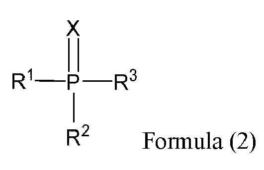
- X
- is selected from 0, S, Se;
- R1 and R2
- are independently selected from C1 to C12 alkyl, C6 to C20 aryl and C5 to C20 heteroaryl;
- R3
- is selected from formula (2A),


- *
- marks the position in the respective R4 or Ar1 group for binding the R4 or Ar1 to the phosphorus atom in formula (I);
- R4
- is selected from C1 to C8 alkyl, C6 to C20 aryl and C5 to C20 heteroaryl;
- Ar1
- is selected from C6 to C20 aryl and C5 to C20 heteroaryl;
- Ar2
- is selected from C18 to C40 aryl and C10 to C40 heteroaryl;
- R5
- is selected from H, C1 to C12 alkyl, C6 to C20 aryl and C5 to C20 heteroaryl
- n
- is selected from 0, 1, or 2.
- at least one redox n-dopant of an elemental metal is selected from the group comprising:
- It has been surprisingly found that the defined layer arrangement comprising a light emitting layer, a hole transport layer and an electron transport layer, wherein the compositions thereof are perfectly matched to one another, increases the power efficiency of an electroluminescent device.
- It has been further surprisingly found that for the defined layer arrangement the use of at least one fluorescent emitter compound embedded in at least one polar emitter host compound enables better device performance in comparison with its non-polar alternatives.
- Further it has been found for the defined layer arrangement of a light emitting layer, a hole transport layer and an electron transport layer, that a proper fit between polarity of the emitter host and polarity of the electron transport layer matrix compound, which forms the electron transport layer adjacent to the emitting layer may has an additional improved effect on device efficiency, for example in state-of-art devices with high brightness, which is enabled by use of redox n-dopant in at least one electron transport layer matrix compound in the electroluminescent device.
- Particular aspects of the device are described in detail below.
- Operation conditions of an electroluminescent device, for example an OLED, are described in the experimental part of this specification.
- According to a further aspect of the invention, the electroluminescent device can be an organic light emitting diode OLED.
- In one embodiment, the OLED comprising the defined layer arrangement may be a tandem OLED, for example a white tandem OLED.
- Similar as other compounds comprised in the inventive device outside the emitting layer, the first electron transport matrix compound may not emit visible light under the operation condition of an electroluminescent device, for example an OLED.
- Under an elemental metal, it is understood a metal in a state of a neat metal, of a metal alloy, or in a state of free atoms or metal clusters. It is understood that metals deposited by vacuum thermal evaporation from a metallic phase, e.g. from a neat bulk metal, vaporize in their elemental form. It is further understood that if the vaporized elemental metal is deposited together with a covalent matrix, the metal atoms and/or clusters are embedded in the covalent matrix. In other words, it is understood that any metal doped covalent material prepared by vacuum thermal evaporation contains the metal at least partially in its elemental form.
- For the use in consumer electronics, only metals containing stable nuclides or nuclides having very long halftime of radioactive decay might be applicable. As an acceptable level of nuclear stability, the nuclear stability of natural potassium can be taken.
- In the present specification, when a definition is not otherwise provided, "substituted" refers to one substituted with a C1 to C10 alkyl.
- In the present specification, when a definition is not otherwise provided, an "alkyl group" refers to a saturated aliphatic hydrocarbyl group. The alkyl group may be a C1 to C10 alkyl group. More specifically, the alkyl group may be a C1 to C10 alkyl group or a C1 to C6 alkyl group. For example, a C1 to C4 alkyl group includes 1 to 4 carbons in alkyl chain, and may be selected from methyl, ethyl, propyl, iso-propyl, n-butyl, iso-butyl, sec-butyl, and t-butyl.
- Specific examples of the alkyl group may be a methyl group, an ethyl group, a propyl group, an isopropyl group, a butyl group, an isobutyl group, a t-butyl group, a pentyl group, a hexyl group.
- In the present specification, "aryl group" refers to a hydrocarbyl group which can be created by formal abstraction of one hydrogen atom from an aromatic ring in the corresponding aromatic hydrocarbon. Aromatic hydrocarbon refers to a hydrocarbon which contains at least one aromatic ring or aromatic ring system. Aromatic ring or aromatic ring system refers to a planar ring or ring system of covalently bound carbon atoms, wherein the planar ring or ring system comprises a conjugated system of delocalized electrons fulfilling Hückel's rule. Examples of aryl groups include monocyclic groups like phenylor tolyl, polycyclic groups which comprise more aromatic rings linked by single bonds, like biphenylyl, and polycyclic groups comprising fused rings, like naphtyl or fluoren-2-yl.
- Analogously, under heteroaryl, it is understood a group derived by formal abstraction of one ring hydrogen from a heterocyclic aromatic ring in a compound comprising at least one such ring.
- Under heterocycloalkyl, it is understood a group derived by formal abstraction of one ring hydrogen from a saturated heterocyclic ring in a compound comprising at least one such ring.
- The term "hetero" is understood the way that at least one carbon atom, in a structure which may be formed by covalently bound carbon atoms, is replaced by another polyvalent atom. Preferably, the heteroatoms are selected from B, Si, N, P, O, S; more preferably from N, P, O, S.
- In the present specification, the single bond refers to a direct bond.
- In the context of the present invention, "different" means that the compounds do not have an identical chemical structure.
- The term "free of', "does not contain", "does not comprise" does not exclude impurities which may be present in the compounds prior to deposition. Impurities have no technical effect with respect to the object achieved by the present invention.
- The term "adjacent" refers to an arrangement of two layers whereby the layers are in direct contact.
- In the context of the present specification the term "essentially non-emissive" means that the contribution of the compound or layer to the visible emission spectrum from the device is less than 10 %, preferably less than 5 % relative to the visible emission spectrum. The visible emission spectrum is an emission spectrum with a wavelength of about ≥ 380 nm to about ≤ 780 nm.
- In the specification, hole characteristics refer to an ability to donate an electron to form a hole when an electric field is applied and that a hole formed in the anode may be easily injected into the emission layer and transported in the emission layer due to conductive characteristics according to a highest occupied molecular orbital (HOMO) level.
- In addition, electron characteristics refer to an ability to accept an electron when an electric field is applied and that electron formed in the cathode may be easily injected into the emission layer and transported in the emission layer due to conductive characteristics according to a lowest unoccupied molecular orbital (LUMO) level.
- Another aspect of the present invention provides an electroluminescent device comprising:
- at least one anode layer,
- at least one cathode layer,
- at least one light emitting layer,
- at least one first hole transport layer,
- at least a first electron transport layer;
- the at least one light emitting layer is arranged between the anode layer and the cathode layer, wherein the at least one light emitting layer comprises:
- at least one fluorescent emitter compound embedded in at least one polar emitter host compound, wherein
- the at least one polar emitter host compound has at least three aromatic rings, which are independently selected from carbocyclic rings and heterocyclic rings, and has a gas phase dipole moment in the range from about ≥ 0.2 Debye to about ≤ 2.0 Debye;
- the at least one first hole transport layer is arranged between the anode layer and the light emitting layer, wherein the at least one first hole transport layer comprises:
- at least one electrical p-dopant of a quinone derivative, a metal oxide and/or a cyano group-containing compound, or
- at least one electrical p-dopant of a quinone derivative, a metal oxide and/or a cyano group-containing compound, and at least one first hole transport matrix compound of a polycyclic aromatic hydrocarbons, triaryl amine compounds and/or heterocyclic aromatic compounds;
- the at least one first electron transport layer is arranged between the cathode layer and the light emitting layer, wherein the first electron transport layer comprises:
- at least one redox n-dopant of an elemental metal, an electrically neutral metal complex and/or an electrically neutral organic radical, and
- at least one first electron transport aromatic matrix compound, wherein the aromatic matrix compound is a compound according to chemical formula (2):

- X
- is selected from O, S, Se;
- R1 and R2
- are independently selected from C1 to C12 alkyl, C6 to C20 aryl and C5 to C20 heteroaryl;
- R3
- is selected from formula (2A),


- *
- marks the position in the respective R4 or Ar1 group for binding the R4 or Ar1 to the phosphorus atom in formula (I);
- R4
- is selected from C1 to C8 alkyl, C6 to C20 aryl and C5 to C20 heteroaryl;
- Ar1
- is selected from C6 to C20 aryl and C5 to C20 heteroaryl;
- Ar2
- is selected from C18 to C40 aryl and C10 to C40 heteroaryl;
- R5
- is selected from H, C1 to C12 alkyl, C6 to C20 aryl and C5 to C20 heteroaryl
- n
- is selected from 0, 1, or 2.
- Another aspect of the present invention provides an electroluminescent device comprising:
- at least one anode layer,
- at least one cathode layer,
- at least one light emitting layer,
- at least one first hole transport layer,
- at least a first electron transport layer;
- the at least one light emitting layer is arranged between the anode layer and the cathode layer, wherein the at least one light emitting layer comprises:
- at least one fluorescent emitter compound, preferably a blue fluorescent emitter compound, embedded in at least one polar emitter host compound, wherein
- the at least one polar emitter host compound has a gas phase dipole moment in the range from about ≥ 0.2 Debye to about ≤ 2.0 Debye and is an anthracene compound represented by the chemical Formula 1:


- A1
- is selected from the group comprising a substituted or unsubstituted C6-C60 aryl or C6-C60 heteroaryl;
- A2
- is selected from the group comprising a substituted or unsubstituted C1 to C10 alkyl group, a substituted or unsubstituted C6-C60 aryl or C6-C60 heteroaryl;
- A3
- is selected from the group comprising a substituted or unsubstituted C1 to C10 alkyl group, a substituted or unsubstituted C6-C60 aryl or C6-C60 heteroaryl;
- A4
- is selected from the group comprising a substituted or unsubstituted C6-C60 aryl or C6-C60 heteroaryl, preferably a C6-C60 heteroaryl;
- the at least one first hole transport layer is arranged between the anode layer and the light emitting layer, wherein the at least one first hole transport layer comprises:
- at least one electrical p-dopant of a tetracyanoquinonedimethane (TCNQ), 2,3,5,6-tetrafluoro-tetracyano-1,4-benzoquinonedimethane (F4-TCNQ), tungsten oxide, molybdenum oxide, and/or a compound according to Formula HT-D1 and PD-2 below:

- at least one electrical p-dopant of a tetracyanoquinonedimethane (TCNQ), 2,3,5,6-tetrafluoro-tetracyano-1,4-benzoquinonedimethane (F4-TCNQ), tungsten oxide, molybdenum oxide, and/or a compound according to Formula HT-D1 and PD-2;
- at least one first hole transport matrix compound of:


- at least one electrical p-dopant of a tetracyanoquinonedimethane (TCNQ), 2,3,5,6-tetrafluoro-tetracyano-1,4-benzoquinonedimethane (F4-TCNQ), tungsten oxide, molybdenum oxide, and/or a compound according to Formula HT-D1 and PD-2 below:
- the at least one first electron transport layer is arranged between the cathode layer and the light emitting layer, wherein the first electron transport layer comprises:
- at least one redox n-dopant of an electropositive metal selected from substantially stable alkali metals, alkaline earth metals, rare earth metals, and transition metals Ti, V, Cr and Mn; preferably from Li, Na, K, Rb, Cs, Mg, Ca, Sr, Ba, Sm, Eu, Tm, Yb; more preferably from Li, Na, K, Rb, Cs, Mg and Yb, even more preferably from Li, Na, Cs and Yb, most preferably from Li, Na and Yb, and
- at least one first electron transport matrix compound, wherein the matrix compound is a compound according to Formula 2 selected from a compound according to formula Va to Vai:
- Formula Va to Ve:


- Formula Vf to Vq:


- Formula Vr to Vt:

- Formula Vu to Vai:


- Formula Va to Ve:
- According to another embodiment of the electroluminescent device, wherein the at least one light emitting layer comprises an emitter host compound comprising 4, 5, 6, 7, 8, 9, 10, 11 or 12 aromatic rings, which are independently selected from carbocyclic rings and heterocyclic rings, preferably at least three aromatic rings in the emitter host compound are condensed aromatic rings, and further preferred at least one aromatic ring of the emitter host compound is a five- or six-membered heterocyclic ring, and in addition preferred at least one aromatic ring is a five-membered heterocyclic ring containing one atom selected from N, O and S, preferably a furan ring.
- According to another embodiment of the electroluminescent device, wherein the at least one first hole transport layer comprises an electrical p-dopant, which is selected from the group comprising:
- a) organic compounds comprising at least one, preferably at least two, more preferably at least three, most preferably at least four electron withdrawing group(s) selected from:
- (i) perhalogenated alkyl, wherein the halogen in the perhalogenated alkyl is preferably selected from F and Cl, more preferably, the perhalogenated alkyl is a perfluoroalkyl,
- (ii) carbonyl group,
- (iii) sulfonyl group,
- (iv) nitrile group and
- (v) nitro group;
- b) metal oxides, metal salts and metal complexes, wherein the metal in the metal oxide, metal salt and/or the metal complex is preferably present in its maximum oxidation state.
- According to another embodiment of the electroluminescent device, wherein the at least one first hole transport layer comprises an electrical p-dopant and at least one first hole transport matrix compound.
- According to another embodiment of the electroluminescent device, wherein the at least one first hole transport matrix compound is selected from the group comprising an organic conjugated aromatic system with at least 6 delocalized electrons.
- According to another embodiment of the electroluminescent device, wherein the at least one first electron transport layer comprises a redox n-dopant, which is selected from the group comprising:
- a) elemental metals, preferably selected from alkali metals, alkaline earth metals and rare earth metals; further preferred selected from Li, Na, K, Rb, Cs, Mg, Ca, Sr, Ba, Sm, Eu, Yb; more preferred selected from Li, Na, Cs, Mg, Sr, Yb; even more preferred selected from Li, Na, Mg, Yb; most preferred selected from Li and/or Yb;
- b) organic radicals, preferably selected from diazolyl radicals, oxazolyl radicals and thiazolyl radicals;
- c) transition metal complexes, wherein the transition metal is selected from 3rd, 4th, 5th 6th, 7rd, 8th, 9th or 10th group of the Periodic Table and is in oxidation state (-I), (0), (I) or (II), preferably, the transition metal complex is electrically neutral.
- According to another embodiment of the electroluminescent device, wherein the at least one first electron transport aromatic matrix compound is selected from the group comprising an organic conjugated aromatic system with at least 6 delocalized electrons.
- According to another embodiment of the electroluminescent device:
- for the at least one light emitting layer:
- the emitter host compound comprises 4, 5, 6, 7, 8, 9, 10, 11 or 12 aromatic rings, which are independently selected from carbocyclic rings and heterocyclic rings, preferably at least three aromatic rings in the emitter host compound are condensed aromatic rings, and further preferred at least one aromatic ring of the emitter host compound is a five- or six-membered heterocyclic ring, and in addition preferred at least one aromatic ring is a five-membered heterocyclic ring containing one atom selected from N, O and S,, preferably a furan ring; and
- for the at least one first hole transport layer:
- the electrical p-dopant is selected from the group comprising:
- a) organic compounds comprising at least one, preferably at least two, more preferably at least three, most preferably at least four electron withdrawing group(s) selected from:
- (i) perhalogenated alkyl, wherein the halogen in the perhalogenated alkyl is preferably selected from F and Cl, more preferably, the perhalogenated alkyl is a perfluoroalkyl,
- (ii) carbonyl group,
- (iii) sulfonyl group,
- (iv) nitrile group and
- (v) nitro group;
- b) metal oxides, metal salts and metal complexes, wherein the metal in the metal oxide, metal salt and/or the metal complex is preferably present in its maximum oxidation state; and
- a) organic compounds comprising at least one, preferably at least two, more preferably at least three, most preferably at least four electron withdrawing group(s) selected from:
- optional at least one first hole transport matrix compound is selected from the group comprising an organic conjugated aromatic system with at least 6 delocalized electrons;
- the electrical p-dopant is selected from the group comprising:
- for the at least one first electron transport layer:
- the redox n-dopant is selected from the group comprising:
- a) elemental metals, preferably selected from alkali metals, alkaline earth metals and rare earth metals; further preferred selected from Li, Na, K, Rb, Cs, Mg, Ca, Sr, Ba, Sm, Eu, Yb; more preferred selected from Li, Na, Cs, Mg, Sr, Yb; even more preferred selected from Li, Na, Mg, Yb; most preferred selected from Li and/or Yb;
- b) organic radicals, preferably selected from diazolyl radicals, oxazolyl radicals and thiazolyl radicals;
- c) transition metal complexes, wherein the transition metal is selected from 3rd, 4th, 5th 6th, 7rd, 8th, 9th or 10th group of the Periodic Table and is in oxidation state (-I), (0), (I) or (II), preferably, the transition metal complex is electrically neutral;
- the at least one first electron transport aromatic matrix compound is selected from the group comprising an organic conjugated aromatic system with at least 6 delocalized electrons.
- the redox n-dopant is selected from the group comprising:
- According to another embodiment of the electroluminescent device, wherein the emitter host compound has a gas phase dipole moment in the range from about ≥ 0.3 Debye to about ≤ 1.8 Debye, preferably in the range from about ≥ 0.5 Debye to about ≤ 1.6 Debye, even more preferred in the range from about ≥ 0.6 Debye to about ≤ 1.4 Debye, and most preferred in the range from about ≥ 0.7 Debye to about ≤ 1.3Debye.
- According to another embodiment of the electroluminescent device, wherein the first electron transport aromatic matrix compound is an organic conjugated aromatic system with at least 6 delocalized electrons comprising a phosphine oxide group.
- According to another embodiment of the electroluminescent device, wherein
- the emitter host compound has a gas phase dipole moment in the range from about ≥ 0.3 Debye to about ≤ 1.8 Debye, preferably in the range from about ≥ 0.5 Debye to about ≤ 1.6 Debye, even more preferred in the range from about ≥ 0.6 Debye to about ≤ 1.4 Debye, and most preferred in the range from about ≥ 0.7 Debye to about ≤ 1.3 Debye; and
- the first electron transport aromatic matrix compound is an organic conjugated aromatic system with at least 6 delocalized electrons comprising a phosphine oxide group.
- According to another embodiment of the electroluminescent device, wherein the emitter host compound is an anthracene compound represented by the chemical Formula 1:

- A1
- is selected from the group comprising a substituted or unsubstituted C6-C60 aryl or C6-C60 heteroaryl;
- A2
- is selected from the group comprising a substituted or unsubstituted C1 to C10 alkyl group, a substituted or unsubstituted C6-C60 aryl or C6-C60 heteroaryl;
- A3
- is selected from the group comprising a substituted or unsubstituted C1 to C10 alkyl group, a substituted or unsubstituted C6-C60 aryl or C6-C60 heteroaryl;
- A4
- is selected from the group comprising a substituted or unsubstituted C6-C60 aryl or C6-C60 heteroaryl, preferably a C6-C60 heteroaryl.
- According to another embodiment of the electroluminescent device, wherein the first electron transport aromatic matrix compound comprising a phosphine oxide group having the chemical formula 2:

- X
- is selected from O, S, Se;
- R1 and R2
- are independently selected from C1 to C12 alkyl, C6 to C20 aryl and C5 to C20 heteroaryl;
- R3
- is selected from formula (2A),

- *
- marks the position in the respective R4 or Ar1 group for binding the R4 or Ar1 to the phosphorus atom in formula (I);
- R4
- is selected from C1 to C8 alkyl, C6 to C20 aryl and C5 to C20 heteroaryl;
- Ar1
- is selected from C6 to C20 aryl and C5 to C20 heteroaryl;
- Ar2
- is selected from C18 to C40 aryl and C10 to C40 heteroaryl;
- R5
- is selected from H, C1 to C12 alkyl, C6 to C20 aryl and C5 to C20 heteroaryl
- n
- is selected from 0, 1, or 2.
- According to another embodiment of the electroluminescent device, wherein
- the emitter host compound is an anthracene compound represented by the chemical Formula 1:

- A1
- is selected from the group comprising a substituted or unsubstituted C6-C60 aryl or C6-C60 heteroaryl;
- A2
- is selected from the group comprising a substituted or unsubstituted C1 to C10 alkyl group, a substituted or unsubstituted C6-C60 aryl or C6-C60 heteroaryl;
- A3
- is selected from the group comprising a substituted or unsubstituted C1 to C10 alkyl group, a substituted or unsubstituted C6-C60 aryl or C6-C60 heteroaryl;
- A4
- is selected from the group comprising a substituted or unsubstituted C6-C60 aryl or C6-C60 heteroaryl, preferably a C6-C60 heteroaryl; and
- the first electron transport aromatic matrix compound comprising a phosphine oxide group having the chemical formula 2:

- X
- is selected from O, S, Se;
- R1 and R2
- are independently selected from C1 to C12 alkyl, C6 to C20 aryl and C5 to C20 heteroaryl;
- R3
- is selected from formula (2A),


- *
- marks the position in the respective R4 or Ar1 group for binding the R4 or Ar1 to the phosphorus atom in formula (I);
- R4
- is selected from C1 to C8 alkyl, C6 to C20 aryl and C5 to C20 heteroaryl;
- Ar1
- is selected from C6 to C20 aryl and C5 to C20 heteroaryl;
- Ar2
- is selected from C18 to C40 aryl and C10 to C40 heteroaryl;
- R5
- is selected from H, C1 to C12 alkyl, C6 to C20 aryl and C5 to C20 heteroaryl
- n
- is selected from 0, 1, or 2.
- According to another embodiment of the electroluminescent device, wherein in chemical Formula 1 the hetero atom of the C6-C60 heteroaryl is selected from the group comprising N, O and/or S, preferably O.
- According to another embodiment of the electroluminescent device, wherein in chemical Formula 2 at least one or all of R1, R2, R5, Ar1 and Ar2 are substituted with C1 to C12 alkyl and C1 to C12 heteroalkyl groups.
- According to another embodiment of the electroluminescent device, wherein
- in chemical Formula 1 the hetero atom of the C6-C60 heteroaryl is selected from the group comprising N, O and/or S, preferably O; and
- in chemical Formula 2 at least one or all of R1, R2, R5, Ar1 and Ar2 are substituted with C1 to C12 alkyl and C1 to C12 heteroalkyl groups.
- According to another embodiment of the electroluminescent device, wherein in chemical Formula 1:
- the C6-C60 heteroaryl comprises at least one five-membered ring, preferably the five membered ring is a furan or thiophene ring; or
- the C6-C60 heteroaryl comprises an anthracene or benzoanthracene; or
- the C6-C60 heteroaryl comprises a benzofuran, dibenzofuran, benzo-naphtofuran or dinaphtofuran.
- According to another embodiment of the electroluminescent device, wherein in chemical Formula 2, two substituents selected from R1, R2 and R3 form with the phosphorus atom a 7-membered phosphepine ring.
- According to another embodiment of the electroluminescent device, wherein
- in chemical Formula 1:
- the C6-C60 heteroaryl comprises at least one five-membered ring, preferably the five membered ring is a furan or thiophene ring; or
- the C6-C60 heteroaryl comprises an anthracene or benzoanthracene; or
- the C6-C60 heteroaryl comprises a benzofuran, dibenzofuran, benzo-naphtofuran and dinaphtofuran; and
- in chemical Formula 2:
- two substituents selected from R1, R2 and R3 form with the phosphorus atom a 7-membered phosphepine ring.
- According to another embodiment of the electroluminescent device, wherein
- in chemical Formula 1:
A4 has the following formulas (IIa) to (IIi):

- According to another embodiment of the electroluminescent device, wherein the anthracene compound according to chemical Formula I is selected from the group of Formula B1 to B7:


- According to another embodiment of the electroluminescent device, wherein the first electron transport aromatic matrix compound comprising a phosphine oxide group according to chemical Formula 2 is selected from the group of Formula Va to Vai:
- Formula Va to Ve:


- Formula Vf to Vq:


- Formula Vr to Vt:

- Formula Vu to Vai:


- According to another embodiment of the electroluminescent device, wherein
- the anthracene compound according to chemical Formula 1 is selected from the group of Formula B1 to B7:


- the first electron transport aromatic matrix compound comprising a phosphine oxide group according to chemical Formula 2 is selected from the group of Formula Va to Vai:
- Formula Va to Ve:


- Formula Vf to Vq:


- Formula Vr to Vt:

- Formula Vu to Vai:


- Formula Va to Ve:
- According to another embodiment of the electroluminescent device, wherein the device comprises in addition a second electron transport layer comprising at least one second electron transport matrix compound, comprising preferably a conjugated system of at least six delocalized electrons, and the second electron transport layer is arranged between the first electron transport layer and the light emitting layer, preferably the second electron transport layer is adjacent arranged to the first electron transport layer and/or to the light emitting layer.
- According to another embodiment of the electroluminescent device, wherein the second electron transport compound is an aromatic compound having a redox potential, measured by the standard procedure, as described below, in the range from -2.2 to -2.4 V, against ferrocene / ferrocenium redox couple as a reference.
- According to another embodiment of the electroluminescent device, wherein the second electron transport aromatic matrix compound has a gas phase dipole moment, computed by the standardized method as described below, in the range from 0.1 Debye to 5.0 Debye, preferably from 0.5 Debye to 4.5 Debye, more preferably from 1.0 Debye to 4.0 Debye, even more preferably from 1.2 Debye to 3.8 Debye, and most preferably from 1.5 Debye to 3.5 Debye.
- The present invention is further described in more detail.
- An electron transport region of the stack of organic layers may be disposed on the emission layer.
- The electron transport region of the stack of organic layers includes at least the first electron transport layer and optional a second electron transport layer. The electron transport region of the stack of organic layers may further include an electron injection layer.
- For example, the electron transport region of the stack of organic layers may have a structure of the first electron transport layer/electron injection or as an alternative a first electron transport layer/second electron transport layer/electron injection layer but is not limited thereto. For example, an organic light emitting diode according to an embodiment of the present invention includes at least one electron transport layer, and in this case, the electron transport layer comprising the electrical p-dopant and the at least one first electron transport matrix compound is defined as the first electron transport layer. In another embodiment, the organic light emitting diode may comprise at least two electron transport layers in the electron transport region of the stack of organic layers, and in this case, the electron transport layer contacting the emission layer is defined as the second electron transport layer.
- The electron transport layer may include one or two or more different electron transport matrix compounds.
- The thickness of the first electron transport layer may be from about 2 nm to about 100 nm, for example about 3 nm to about 30 nm. When the thickness of the first electron transport layer is within these ranges, the first electron transport layer may have improved electron transport auxiliary ability without a substantial increase in driving voltage.
- A thickness of the optional second electron transport layer may be about 10 nm to about 100 nm, for example about 15 nm to about 50 nm. When the thickness of the electron transport layer is within these ranges, the electron transport layer may have satisfactory electron transporting ability without a substantial increase in driving voltage.
- First electron transport matrix is not particularly limited. Similarly as other materials which are in the inventive device comprised outside the emitting layer, the second electron transport matrix may not emit light.
- According to one embodiment, the first electron transport matrix can be an organic compound, an organometallic compound, or a metal complex.
- According to one embodiment, the first electron transport matrix may be a covalent compound comprising a conjugated system of at least 6 delocalized electrons. Under a covalent material in a broadest possible sense, it might be understood a material, wherein at least 50 % of all chemical bonds are covalent bonds, wherein coordination bonds are also considered as covalent bonds. In the present application, the term encompasses in the broadest sense all usual electron transport matrices which are predominantly selected from organic compounds but also e.g. from compounds comprising structural moieties which do not comprise carbon, for example substituted 2,4,6-tribora-1,3,5 triazines, or from metal complexes, for example aluminium tris(8-hydroxyquinolinolate).
- The molecular covalent materials can comprise low molecular weight compounds which may be, preferably, stable enough to be processable by vacuum thermal evaporation (VTE). Alternatively, covalent materials can comprise polymeric covalent compounds, preferably, compounds soluble in a solvent and thus processable in form of a solution. It is to be understood that a polymeric substantially covalent material may be crosslinked to form an infinite irregular network, however, it is supposed that such crosslinked polymeric substantially covalent matrix compound still comprises both skeletal as well as peripheral atoms. Skeletal atoms of the covalent compound are covalently bound to at least two neighbour atoms. Other atoms of the covalent compound are peripheral atoms which are covalently bound with a single neighbour atom. Inorganic infinite crystals or fully crosslinked networks having partly covalent bonding but substantially lacking peripheral atoms, like silicon, germanium, gallium arsenide, indium phosphide, zinc sulfide, silicate glass etc are not considered as covalent matrices in the sense of present application, because such fully crosslinked covalent materials comprise peripheral atoms only on the surface of the phase formed by such material. A compound comprising cations and anions is still considered as covalent, if at least the cation or at least the anion comprises at least ten covalently bound atoms.
- Preferred examples of covalent first electron transport matrix compounds are organic compounds, consisting predominantly from covalently bound C, H, O, N, S, which may optionally comprise also covalently bound B, P, As, Se. In one embodiment, the first electron transport matrix compound lacks metal atoms and majority of its skeletal atoms is selected from C, O, S, N.
- In another embodiment, the first electron transport matrix compound comprises a conjugated system of at least six, more preferably at least ten, even more preferably at least fourteen delocalized electrons.
- Examples of conjugated systems of delocalized electrons are systems of alternating pi- and sigma bonds. Optionally, one or more two-atom structural units having the pi-bond between its atoms can be replaced by an atom bearing at least one lone electron pair, typically by a divalent atom selected from O, S, Se, Te or by a trivalent atom selected from N, P, As, Sb, Bi. Preferably, the conjugated system of delocalized electrons comprises at least one aromatic or heteroaromatic ring adhering to the Hückel rule. Also preferably, the first electron transport matrix compound may comprise at least two aromatic or heteroaromatic rings which are either linked by a covalent bond or condensed.
- In one of specific embodiments, the first electron transport matrix compound comprises a ring consisting of covalently bound atoms and at least one atom in the ring is phosphorus.
- In a more preferred embodiment, the phosphorus-containing ring consisting of covalently bound atoms is a phosphepine ring.
- In another preferred embodiment, the first electron transport compound comprises a phosphine oxide group. Also preferably, the s first electron transport matrix compound comprises a heterocyclic ring comprising at least one nitrogen atom. Examples of nitrogen containing heterocyclic compounds which are particularly advantageous as first electron transport matrix compound for the inventive device are matrices comprising, alone or in combination, pyridine structural moieties, diazine structural moieties, triazine structural moieties, quinoline structural moieties, benzoquinoline structural moieties, quinazoline structural moieties, acridine structural moieties, benzacridine structural moieties, dibenzacridine structural moieties, diazole structural moieties and benzodiazole structural moieties.
- The first electron transport matrix compound may have a molecular weight (Mw) of ≥ 400 to ≤ 850 g / mol, preferably ≥ 450 to ≤ 830 g / mol. If the molecular weight is selected in this range, particularly reproducible evaporation and deposition can be achieved in vacuum at temperatures where good long-term stability is observed.
- Preferably, the first electron transport matrix compound may be essentially non-emissive.
- In another embodiment, the first electron transport matrix compound may have dipole moment higher than 2.3 Debye. It may be a preferred embodiment in combination with redox dopants selected from elemental metals.
- According to a further aspect of the invention, the reduction potential of the first electron transport matrix compound, if measured under the same conditions by cyclic voltammetry against Fc/Fc+ in tetrahydrofuran, may have a value which is less negative than the value obtained for triphenylphosphine oxide and more negative than the value obtained for tetrakis(quinoxalin-5-yloxy)zirconium.
- Under these conditions the redox potential of triphenylphosphine oxide is about -3.06 V and the reduction potential of tetrakis(quinoxalin-5-yloxy)zirconium is about -1.78 V.
- According to a further aspect of the invention, the redox potential of the first electron transport matrix compound, if measured under the same conditions by cyclic voltammetry against Fc/Fc+ in tetrahydrofuran, may have a value which is less negative than the respective value obtained for triphenylphosphine oxide, preferably less negative than the respective value for bis(4-(9H-carbazol-9-yl)phenyl)- (phenyl)phosphine oxide, more preferably less negative than the respective value for 3-([1,1'-biphenyl]-4-yl)-5-(4-(tert-butyl)phenyl)-4-phenyl-4H-1,2,4-triazole, even more preferably less negative than the respective value for pyrene, most preferably less negative than the respective value for 2,7-di-pyrenyl-9,9-spirobifluorene, also preferably less negative than the respective value for 4,7-diphenyl-1,10-phenanthroline, also preferably less negative than the respective value for 2,4,7,9-tetraphenyl-1,10-phenanthroline, also preferably less negative than the respective value for 7-([1,1'-biphenyl]-4-yl)dibenzo[c,h]acridine, also preferably less negative than the respective value for 2,4,6-triphenyltriazine, and still preferably less negative than the respective value for 2,4,6-tri(biphenyl-4-yl)-1,3,5-triazine.
- According to a further aspect of the invention, the redox potential of the first electron transport matrix compound, if measured under the same conditions by cyclic voltammetry against Fc/Fc+ in tetrahydrofuran, may have the value which is more negative than the respective value obtained for tetrakis(quinoxalin-5-yloxy)zirconium, preferably more negative than the respective value for 4,4'-bis(4,6-diphenyl-1,3,5-triazin-2-yl)-1,1'-biphenyl, most preferably more negative than the respective value for 2,4,6-tri(biphenyl-4-yl)-1,3,5-triazine.
- The redox potential can be determined by following standard method, using cyclic voltammetry with potentiostatic device Metrohm PGSTAT30 and software Metrohm Autolab GPES at room temperature. The redox potentials given at particular compounds are measured in an argon de-aerated, dry 0.1M THF solution of the tested substance, under argon atmosphere, with 0.1M tetrabutylammonium hexafluorophosphate supporting electrolyte, between platinum working electrodes and with an Ag/AgCl pseudo-standard electrode (Metrohm Silver rod electrode), consisting of a silver wire covered by silver chloride and immersed directly in the measured solution, with the
scan rate 100 mV/s. The first run is done in the broadest range of the potential set on the working electrodes, and the range was then adjusted within subsequent runs appropriately. The final three runs are done with the addition of ferrocene (in 0.1M concentration) as the standard. The average of potentials corresponding to cathodic and anodic peak of the studied compound, after subtraction of the average of cathodic and anodic potentials observed for the standard Fc+/Fc redox couple, afford finally the values reported above. All studied compounds as well as the reported comparative compounds showed well-defined reversible electrochemical behaviour. - According to various embodiments of the electroluminescent device the first electron transport matrix compound can be selected from:
- an anthracene compound substituted with aryl, heteroaryl or alkyl groups, e.g. 3-[3'-(10-phenyl-9-anthracenyl)[1,1'-biphenyl]-4-yl]- quinoline;
- a benzimidazole compound substituted with aryl, heteroaryl or alkyl groups, preferably 2-(4-(9,10-di(naphthalen-2-yl)anthracene-2-yl)phenyl)-1-phenyl- 1H-benzo[d]imidazole and/or 1-(4-(10-([1,1'-biphenyl]-4-yl)anthracen-9-yl)phenyl)-2-ethyl-1H-benzo[d]imidazole;
- a phosphine oxide compound substituted with aryl, heteroaryl or alkyl groups, preferably (3-(dibenzo[c,h]acridin-7-yl)phenyl)diphenylphosphine oxide, 3-phenyl-3H-benzo[b]dinaphtho[2,1-d:1',2'-f]phosphepine-3-oxide, phenyldi(pyren-1-yl)phosphine oxide, bis(4-(anthracen-9-yl)phenyl)(phenyl)phosphine oxide, (3-(9,10-di(naphthalen-2-yl)anthracen-2-yl)phenyl)diphenylphosphine oxide, phenyldi(pyren-1-yl)phosphine oxide, diphenyl(5-(pyren-1-yl)pyridin-2-yl)phosphine oxide, diphenyl(4'-(pyren-1-yl)-[1,1'-biphenyl]-3-yl)phosphine oxide, diphenyl(4'-(pyren-1-yl)-[1,1'-biphenyl]-3-yl)phosphine oxide, (3'-(dibenzo[c,h]acridin-7-yl)-[1,1'-biphenyl]-4-yl)diphenylphosphine oxide and/or phenyl bis(3-(pyren-1-yl)phenyl)phosphine oxide;
- a phenanthroline compound substituted with aryl or heteroaryl groups, preferably 2,4,7,9-tetraphenyl-1,10-phenanthroline, 4,7-diphenyl-2,9-di-p-tolyl-1,10-phenanthroline, 2,9-di(biphenyl-4-yl)-4,7-diphenyl-1,10-phenanthroline, 1,3-bis(9-phenyl-1,10-phenanthrolin-2-yl)benzene and/or 3,8-bis(6-phenyl-2-pyridinyl)- 1,10-phenanthroline;
- a quinazoline compound substituted with aryl or heteroaryl groups, preferably 9-phenyl-9'-(4-phenyl-2-quinazolinyl)- 3,3'-bi-9H-carbazole;
- a benzo[h]quinazoline compound substituted with aryl or heteroaryl groups, preferably 4-(2-naphthalenyl)-2-[4-(3-quinolinyl)phenyl]- benzo[h]quinazoline;
- a pyrido[3,2-h]quinazoline compound substituted with aryl or heteroaryl groups, preferably 4-(naphthalen-1-yl)-2,7,9-triphenylpyrido[3,2-h]quinazoline;
- a triazine compound substituted with aryl or heteroaryl groups, preferably 4,4'-bis(4,6-diphenyl-1,3,5-triazin-2-yl)biphenyl, 3-[4-(4,6-di-2-naphthalenyl-1,3,5-triazin-2-yl) phenyl]quinoline and/or 2-[3-(6'-methyl[2,2'-bipyridin]-5-yl)-5-(9-phenanthrenyl)phenyl]-4,6-diphenyl-1,3,5-triazine and / or
- an acridine compound substituted with aryl or heteroaryl groups, preferably 7-(naphthalen-2-yl)dibenzo[c,h]acridine.
- According to various embodiments of the electroluminescent device a matrix compound for the first electron transport layer can be more preferred; whereby the matrix compound of the second electron transport layer preferably differs from the first electron transport layer, can be selected from a phosphine oxide compound substituted with aryl, heteroaryl or alkyl groups, preferably (3-(dibenzo[c,h]acridin-7-yl)phenyl)diphenylphosphine oxide, 3-phenyl-3H-benzo[b]dinaphtho[2,1-d:1',2'-f]phosphepine-3-oxide, phenyldi(pyren-1-yl)phosphine oxide, bis(4-(anthracen-9-yl)phenyl)(phenyl)phosphine oxide, (3-(9,10-di(naphthalen-2-yl)anthracen-2-yl)phenyl)diphenylphosphine oxide, diphenyl(5-(pyren-1-yl)pyridin-2-yl)phosphine oxide, diphenyl(4'-(pyren-1-yl)-[1,1'-biphenyl]-3-yl)phosphine oxide, diphenyl(4'-(pyren-1-yl)-[1,1'-biphenyl]-3-yl)phosphine oxide, (3'-(dibenzo[c,h]acridin-7-yl)-[1,1'-biphenyl]-4-yl)diphenylphosphine oxide and/or phenyl bis(3-(pyren-1-yl)phenyl)phosphine oxide.
- Suitable matrix compounds that can be suitable used for the first electron transport layer are summarized in Table 1 below.
Table 1 Chemical structures of the first ETL-matrix compound that can be suitable used Compound Name Structure Reference MX 1 2-(4-(9, 10-di(naphthalen-2-yl)anthracen-2-yl)phenyl)- 1-phenyl- 1H-benzo [d] imidazole 
US 6878469 MX 2 3-[3'-(10-phenyl-9-anthracenyl)[1,1'-biphenyl]-4-yl]- quinoline 
KR2011018195 MX 3 1-(4-(10-([1,1'-biphenyl]-4-yl)anthracen-9-yl)phenyl)-2-ethyl-1H-benzo [d] imidazole 
WO201013435 2 MX 4 (3'-(dibenzo[c,h]acridin-7-yl)-[1,1'-biphenyl]-4-yl)diphenylphosphine oxide 
EP 2395571 ,WO201307921 7 MX 5 (3-(9,10-di(naphthalen-2-yl)anthracen-2-yl)phenyl)diphenylphosphine oxide 
EP13187905.8 MX 6 bis(4-(anthracen-9-yl)phenyl)(phenyl)phosphine oxide 
EP13187905.8 MX 7 Phenyldi(pyren-1-yl)phosphine oxide 
JP4876333 MX 8 Phenylbis(3 -(pyren- 1 - yl)phenyl)phosphine oxide 
EP13187905.8 MX 9 diphenyl(4'-(pyren-1-yl)-[1,1'-biphenyl]-3-yl)phosphine oxide 
EP13187905.8 MX 10 diphenyl(5-(pyren-1-yl)pyridin-2-yl)phosphine oxide 
WO201416702 0 MX 11 (3-(dibenzo[c,h]acridin-7-yl)phenyl)diphenylphosphine oxide 
EP 2395571 ,WO201307921 7 Vr 3-Phenyl-3H-benzo[b]dinaphtho[2,1-d: 1,2'-f]phosphepine-3-oxide 
EP13199361.0 MX 12 (3-(10-(naphtalen-2-yl)anthracen-9-yl)phenyl)diphenylphosphine oxide 
WO201505228 4 MX 13 2,4,7,9-tetraphenyl-1,10-phenanthroline 
EP1786050 MX 14 4,7-diphenyl-2,9-di-p-tolyl-1,10-phenanthroline 
EP1786050 MX 15 2,9-di(biphenyl-4-yl)-4,7-diphenyl-1,10-phenanthroline 
EP1786050 MX 16 1,3-bis(9-phenyl-1,10-phenanthrolin-2-yl)benzene 
JP2004281390 MX 17 3,8-bis(6-phenyl-2-pyridinyl)- 1,10-phenanthroline 
CN102372708 MX 18 9-phenyl-9'-(4-phenyl-2-quinazolinyl)- 3, 3'-bi-9 H -carbazole 
KR2012102374 MX 19 4-(2-naphthalenyl)-2-[4-(3-quinolinyl) phenyl]- benzo[ h ]quinazoline 
KR2014076522 MX 20 4-(naphthalen-1-yl)-2,7,9-triphenylpyrido [3 ,2-h] quinazoline 
EP1970371 MX 21 4,4'-bis(4,6-diphenyl-1,3,5-triazine-2-yl)biphenyl 
US6225467 MX 22 3-[4-(4,6-di-2-naphthalenyl-1,3,5-triazin-2-yl)phenyl]- quinoline 
US2011015601 3 MX 23 2-[3-(6'-methyl[2,2'-bipyridin]-5-yl)-5-(9-phenanthrenyl)phenyl] -4,6-diphenyl-1,3, 5-triazine 
WO201417154 1 MX 24 7-(naphthalen-2-yl)dibenzo[c,h]acridine 
EP 2395571 - According to various embodiments of the electroluminescent device, wherein the first electron transport layer comprises about ≤ 100 wt.-% to about ≥ 30 wt.-%, preferably ≤ 95 wt.-% to about ≥ 40 wt.-%, of a matrix compound, based on the total weight of the first electron transport layer.
- Preferably, the first electron transport matrix compound may be essentially non-emissive.
- Second electron transport compound is not particularly limited. Similarly as other materials which are in the inventive device comprised outside the emitting layer, the second electron transport matrix may not emit light.
- According to one embodiment, the second electron transport matrix compound can be an organic compound, an organometallic compound, or a metal complex.
- Compounds listed as examples of the first electron transport matrix compound can be used also as the second electron transport matrix compound.
- According to one embodiment, the device comprises in addition a second electron transport layer comprising at least one second electron transport matrix compound which is selected from covalent compounds comprising a conjugated system of at least 6 delocalized electrons, preferably from organic compounds comprising at least one aromatic ring, more preferably from organic compounds comprising at least two aromatic rings, even more preferably from organic compounds comprising at least three aromatic rings, most preferably from organic compounds comprising at least four aromatic rings; and the second electron transport layer is arranged between the first electron transport layer and the light emitting layer, preferably the second hole transport layer is formed of the second electron transport matrix compound, and further preferably the second electron transport layer is adjacent arranged to the first electron transport layer and/or to the light emitting layer.
- According to one embodiment, the second electron transport matrix compound may be a covalent compound comprising a conjugated system of at least 6 delocalized electrons.
In one embodiment, the dipole moment of the second electron transport matrix compound is selected ≥ 0.5 Debye and ≤ 4.5 Debye, preferably ≥ 1.0 Debye and < 4.0 Debye, more preferably ≥ 1.5 Debye and < 3.5 Debye. - According to a further aspect of the invention, the redox potential of the second electron matrix compound may be selected less negative than -2.35 V and more negative than -2.14 V, preferably less negative than -2.3 V and more negative than -2.16 V, more preferably less negative than -2.25 V and more negative than -2.16 V, when measured against Fc/Fc+ in tetrahydrofuran.
- Under redox n-dopant, it is understood a compound which, if embedded into an electron transport matrix, increases concentration of free electrons in comparison with the neat matrix under the same physical condictions measured by cyclic voltammetry against ferrocene/ferrocenium reference redox couple.
- The redox n-dopant may not emit light under the operation condition of an electroluminescent device, for example an OLED. In one embodiment, the redox n-dopant is selected from an elemental metal, an electrically neutral metal complex and/or an electrically neutral organic radical.
- The most practical benchmark for the strength of an n-dopant is the value of its redox potential. There is no particular limitation in terms how negative the value of the redox potential can be.
- As redox potentials of usual electron transport matrices used in organic light emitting diodes are, if measured by cyclic voltammetry against ferrocene/ferrocenium reference redox couple, roughly in the range from about - 1.8 V to about - 3.1V; the practically applicable range of redox potentials for n-dopants which can effectively n-dope such matrices is in a slightly broader range, from about - 1.7 V to about - 3.3 V.
- The measurement of redox potentials is practically performed for a corresponding redox couple consisting of the reduced and of the oxidized form of the same compound.
In case that the redox n-dopant is an electrically neutral metal complex and/or an electrically neutral organic radical, the measurement of its redox potential is actually performed for the redox couple formed by - (i) the electrically neutral metal complex and its cation radical formed by an abstraction of one electron from the electrically neutral metal complex, or
- (ii) the electrically neutral organic radical and its cation formed by an abstraction of one electron from the electrically neutral organic radical.
- Preferably, the redox potential of the electrically neutral metal complex and/or of the electrically neutral organic radical may have a value which is more negative than - 1.7 V, preferably more negative than - 1.9 V, more preferably more negative than - 2.1 V, even more preferably more negative than - 2.3 V, most preferably more negative than - 2.5 V, if measured by cyclic voltammetry against ferrocene/ferrocenium reference redox couple for a corresponding redox couple consisting of
- (i) the electrically neutral metal complex and its cation radical formed by an abstraction of one electron from the electrically neutral metal complex, or
- (ii) the electrically neutral organic radical and its cation formed by an abstraction of one electron from the electrically neutral organic radical.
- In a preferred embodiment, the redox potential of the n-dopant is between the value which is about 0.5 V more positive and the value which is about 0.5 V more negative than the value of the reduction potential of the chosen electron transport matrix.
Electrically neutral metal complexes suitable as redox n-dopants may be e.g. strongly reductive compelxes of some transition metals in low oxidation state. Particularly strong redox n-dopants may be selected for example from Cr(II), Mo(II) and/or W(II) guanidinate complexes such as W2(hpp)4, as described in more detail inWO2005/086251 . - Electrically neutral organic radicals suitable as redox n-dopants may be e.g. organic radicals created by supply of additional energy from their stable dimers, oligomers or polymers, as described in more detail in
EP 1 837 926 B1 ,WO2007/107306 , orWO2007/107356 . Specific examples of such suitable radicals may be diazolyl radicals, oxazolyl radicals and/or thiazolyl radicals. - Under an elemental metal, it is understood a metal in a state of a neat metal, of a metal alloy, or in a state of free atoms or metal clusters. It is understood that metals deposited by vacuum thermal evaporation from a metallic phase, e.g. from a neat bulk metal, vaporize in their elemental form. It is further understood that if the vaporized elemental metal is deposited together with a covalent matrix, the metal atoms and/or clusters are embedded in the covalent matrix. In other words, it is understood that any metal doped covalent material prepared by vacuum thermal evaporation contains the metal at least partially in its elemental form.
- For the use in consumer electronics, only metals containing stable nuclides or nuclides having very long halftime of radioactive decay might be applicable. As an acceptable level of nuclear stability, the nuclear stability of natural potassium can be taken.
- In one embodiment, the n-dopant is selected from electropositive metals selected from alkali metals, alkaline earth metals, rare earth metals and metals of the first transition period Ti, V, Cr and Mn. Preferably, the n-dopant is selected from_Li, Na, K, Rb, Cs, Mg, Ca, Sr, Ba, Sm, Eu, Tm, Yb; more preferably from Li, Na, K, Rb, Cs, Mg and Yb, even more preferably from Li, Na, Cs and Yb, most preferably from Li, Na and Yb.
- The redox dopant may be essentially non-emissive.
- The hole injection layer may improve interface properties between the anode and an organic material used for the hole transport layer, and is applied on a non-planarized anode and thus planarizes the surface of the anode. For example, the hole injection layer may include a material having a median value of the energy level of its highest occupied molecular orbital (HOMO) between the work function of the anode material and the energy level of the HOMO of the hole transport layer, in order to adjust a difference between the work function of the anode and the energy level of the HOMO of the hole transport layer.
- When the hole transport region includes a
hole injection layer 36, the hole injection layer may be formed on the anode by any of a variety of methods, for example, vacuum deposition, spin coating, casting, Langmuir-Blodgett (LB) method, or the like. - When hole injection layer is formed using vacuum deposition, vacuum deposition conditions may vary depending on the material that is used to form the hole injection layer, and the desired structure and thermal properties of the hole injection layer to be formed and for example, vacuum deposition may be performed at a temperature of about 100 °C to about 500 °C, a pressure of about 10-6 Pa to about 10-1 Pa, and a deposition rate of about 0.1 to about 10 nm/sec, but the deposition conditions are not limited thereto.
- When the hole injection layer is formed using spin coating, the coating conditions may vary depending on the material that is used to form the hole injection layer, and the desired structure and thermal properties of the hole injection layer to be formed. For example, the coating rate may be in the range of about 2000 rpm to about 5000 rpm, and a temperature at which heat treatment is performed to remove a solvent after coating may be in a range of about 80 °C to about 200 °C, but the coating conditions are not limited thereto.
- Conditions for forming the hole transport layer and the electron blocking layer may be defined based on the above-described formation conditions for the hole injection layer.
- A thickness of the hole transport part of the charge transport region may be from about 10 nm to about 1000 nm, for example, about 10 nm to about 100 nm. When the hole transport transport part of the charge transport region includes the hole injection layer and the hole transport layer, a thickness of the hole injection layer may be from about 10 nm to about 1000 nm, for example about 10 nm to about 100 nm and a thickness of the hole transport layer may be from about 5 nm to about 200 nm, for example about 10 nm to about 150 nm. When the thicknesses of the hole transport part of the charge transport region, the HIL, and the HTL are within these ranges, satisfactory hole transport characteristics may be obtained without a substantial increase in driving voltage.
- Hole transport matrix materials used in the hole transport region are not particularly limited. Preferred are covalent compounds comprising a conjugated system of at least 6 delocalized electrons, preferably organic compounds comprising at least one aromatic ring, more preferably organic compounds comprising at least two aromatic rings, even more preferably organic compounds comprising at least three aromatic rings, most preferably organic compounds comprising at least four aromatic rings. Typical examples of hole transport matrix materials which are widely used in hole transport layers are polycyclic aromatic hydrocarbons, triaryl amine compounds and heterocyclic aromatic compounds. Suitable ranges of frontier orbital energy levels of hole transport matrices useful in various layer of the hole transport region are well-known. In terms of the redox potential of the redox couple HTL matrix/ cation radical of the HTL matrix, the preferred values (if measured for example by cyclic voltammetry against ferrocene/ferrocenium redox couple as reference) may be in the range 0.0 - 1.0 V, more preferably in the range 0.2 - 0.7 V, even more preferably in the range 0.3 - 0.5 V.
- The hole transport region of the stack of organic layers shall further include an electrical p-dopant improving conductivity and/or hole injection from the anode, in addition to the materials as described above.
- The charge-generating material may be homogeneously or inhomogeneously dispersed in the first hole transport layer.
- The electrical p-dopant may be one of a quinone derivative, a radialene compound, a metal oxide, and a cyano group-containing compound, but is not limited thereto. Nonlimiting examples of the p-dopant are quinone derivatives such as tetracyanoquinonedimethane (TCNQ), 2,3,5,6-tetrafluoro-tetracyano-1,4-benzoquinonedimethane (F4-TCNQ), radialene compounds like PD-2 and the like; metal oxides such as tungsten oxide, molybdenum oxide, and the like; and cyano-containing compounds such as compound HT-D1 below.

- The hole transport part of the charge transport region may further include a buffer layer.
- Buffer layer that can be suitable used are disclosed in
US 6 140 763 ,US 6 614 176 and inUS2016/248022 . - The buffer layer may compensate for an optical resonance distance of light according to a wavelength of the light emitted from the EML, and thus may increase efficiency.
- The emission layer (EML) may be formed on the hole transport region by using vacuum deposition, spin coating, casting, LB method, or the like. When the emission layer is formed using vacuum deposition or spin coating, the conditions for deposition and coating may be similar to those for the formation of the hole injection layer, though the conditions for the deposition and coating may vary depending on the material that is used to form the emission layer. The emission layer may include an emitter host (EML host) and an emitter dopant (further only emitter).
- The emitter may be a red, green, or blue emitter.
- In one embodiment, the emitter host material is a polar emitter host compound, which has a has a gas phase dipole moment in the range from about ≥ 0.2 Debye to about ≤ 2.0 Debye.
- In one embodiment, the emitter host material is a polar emitter host compound having at least three aromatic rings, which are independently selected from carbocyclic rings and heterocyclic rings, which has a has a gas phase dipole moment in the range from about ≥ 0.2 Debye to about ≤ 2.0 Debye.
- In one embodiment, the emitter host material is a polar emitter host compound represented by the chemical Formula 1:

- A1
- is selected from the group comprising a substituted or unsubstituted C6-C60 aryl or C6-C60 heteroaryl;
- A2
- is selected from the group comprising a substituted or unsubstituted C1 to C10 alkyl group, a substituted or unsubstituted C6-C60 aryl or C6-C60 heteroaryl;
- A3
- is selected from the group comprising a substituted or unsubstituted C1 to C10 alkyl group, a substituted or unsubstituted C6-C60 aryl or C6-C60 heteroaryl;
- A4
- is selected from the group comprising a substituted or unsubstituted C6-C60 aryl or C6-C60 heteroaryl, preferably a C6-C60 heteroaryl.
- The polar emitter host compound has at least three aromatic rings, which are independently selected from carbocyclic rings and heterocyclic rings.
- The polar emitter host compound has a gas phase dipole moment in the range from about ≥ 0.2 Debye to about ≤ 2.0 Debye.
- According to one embodiment of electroluminescent device the polar emitter host compound has at least three aromatic rings, which are independently selected from carbocyclic rings and heterocyclic rings, and has a gas phase dipole moment in the range from about ≥ 0.2 Debye to about ≤ 2.0 Debye.
In another embodiment, the emitter host compound has a gas phase dipole moment in the range from about ≥ 0.3 Debye to about ≤ 1.8 Debye, preferably in the range from about ≥ 0.5 Debye to about ≤ 1.6 Debye, even more preferred in the range from about ≥ 0.6 Debye to about ≤ 1.4 Debye, and most preferred in the range from about ≥ 0.7 Debye to about ≤ 1.3 Debye. - The dipole moment |
µ | of a molecule containing N atoms is given by:

r l are the partial charge and position of atom i in the molecule. - The partial charges and atomic positions are computed for a molecule in a gas phase, by a standardized method, using the hybrid functional B3LYP with a Gaussian 6-31G∗ basis set as implemented in the program package TURBOMOLE V6.5. If more than one conformation is viable, the conformation with the lowest total energy is selected to determine the dipole moment.
- The dipole moments and redox potentials of selected compounds which are suitable as the second electron transport matrix compound are given in Table 2.
Table 2 Compound Name Structure Dipole moment / B3LYP_Gaus sian+6-31G∗ Redox potential against Fc/Fc+ in THF / V ETM-1 7-(3-(pyren-1-yl)phenyl)dib enzo[c,h]acri dine 
1.88 -2.26 ETM-2 7-(3-(pyren-1-yl)phenyl)be nzo[c]acridin e 
2.04 -2.2 ETM-3 NET-441 A06391 2-(3'-(4,6-diphenyl-1,3,5-triazin-2-yl)-[1,1'-biphenyl]-3-yl)-4-phenylbenzo[ 4,5]thieno[3, 2-d]pyrimidine 
2.84 -2.20 ETM-4 GH0408S A06539 2-phenyl-4-(4',5',6'-triphenyl-[1,1':2',1":3", 1‴-quaterphenyl ]-3‴-yl)benzo[4,5] thieno[3,2-d]pyrimidine 
1.72 -2.23 ETM-5 
0.30 -2.18 ETM-6 
-/0.66/1.03 -2.22 ETM-7 7-(4',5',6'-triphenyl-[1,1':2',1":3", 1‴-quaterphenyl ]-3‴-yl)-dibenzo[c,h]a cridine 
2.74 -2.29 ETM-8 2,9-di(biphenyl-4-yl)-4,7-diphenyl-1,10-phenanthroli ne (CAS 338734-83-1) 
3.03 -2.29 ETM-9 2,4,7,9-tetraphenyl-1,10-phenanthroli ne (CAS 51786-73-3) 
3.11 -2.33 ETM-10 
0.59 -2.20 ETM-11 
0.66 -2.20 - According to a further aspect of the invention, the emitter host respectively has a redox potential which, if measured under the same conditions by cyclic voltammetry against Fc/Fc+ in tetrahydrofuran, has a value more negative than the respective value obtained for 7-([1,1'-biphenyl]-4-yl)dibenzo[c,h]acridine, preferably more negative than the respective value for 9,9',10,10'-tetraphenyl-2,2'-bianthracene, more preferably more negative than the respective value for 2,9-di([1,1'-biphenyl]-4-yl)-4,7-diphenyl-1,10-phenanthroline, even more preferably more negative than the respective value for 2,4,7,9-tetraphenyl-1,10-phenanthroline, even more preferably more negative than the respective value for 9,10-di(naphthalen-2-yl)-2-phenylanthracene, even more preferably more negative than the respective value for 2,9-bis(2-methoxyphenyl)-4,7-diphenyl-1,10-phenanthroline, most preferably more negative than the respective value for 9,9'-spirobi[fluorene]-2,7-diylbis(diphenylphosphine oxide).
- The emitter is mixed in a small amount to cause light emission. The emitter may be, for example an inorganic, organic, or organometallic compound, and one or more kinds thereof may be used.
- The emitter may be a fluorescent emitter; for example ter-fluorene, 4.4'-bis(4-diphenyl aminostyryl)biphenyl (DPAVBi), 2,5,8,11-tetra-tert-butyl perylene (TBPe), and Compound 4 below are examples of fluorescent blue emitters.

- A thickness of the emission layer may be about 10 nm to about 100 nm, for example about 20 nm to about 60 nm. When the thickness of the emission layer is within these ranges, the emission layer may have improved emission characteristics without a substantial increase in a driving voltage.
- According to another aspect of the invention, the organic electroluminescent device may further comprise an electron injection layer between the first electron transport layer and the cathode.
- The electron injection layer (EIL) may facilitate injection of electrons from the cathode.
- According to another aspect of the invention, the electron injection layer comprises:
- (i) an electropositive metal selected from alkali metals, alkaline earth metals and rare earth metals in substantially elemental form, preferably selected from Li, Na, K, Rb, Cs, Mg, Ca, Sr, Ba, Eu and Yb, more preferably from Li, Na, Mg, Ca, Sr and Yb, even more preferably from Li and Yb, most preferably Yb; and/or
- (ii) an alkali metal complex and/or alkali metal salt, preferably the Li complex and/or salt, more preferably a Li quinolinolate, even more preferably a lithium 8-hydroxyquinolinolate, most preferably the alkali metal salt and/or complex of the second electron transport layer is identical with the alkali metal salt and/or complex of the injection layer.
- The electron injection layer may include at least one selected from LiF, NaCl, CsF, Li2O, and BaO.
- A thickness of the EIL may be from about 0.1 nm to about 10 nm, or about 0.3 nm to about 9 nm. When the thickness of the electron injection layer is within these ranges, the electron injection layer may have satisfactory electron injection ability without a substantial increase in driving voltage.
- A material for the cathode may be a metal, an alloy, or an electrically conductive compound that have a low work function, or a combination thereof. Specific examples of the material for the cathode may be lithium (Li), magnesium (Mg), aluminum (Al), aluminum-lithium (Al-Li), calcium (Ca), magnesium-indium (Mg-In), magnesium-silver (Mg-Ag), etc. In order to manufacture a top-emission light-emitting device having a reflective anode deposited on a substrate, the cathode may be formed as a transmissive electrode from, for example, indium tin oxide (ITO) or indium zinc oxide (IZO).
- In devices comprising a transparent metal oxide cathode or a reflective metal cathode, the cathode may have a thickness from about 50 nm to about 100 nm, whereas semitransparent metal cathodes may be as thin as from about 5 nm to about 15 nm.
- A material for the anode may be a metal or a metal oxide, or an organic material, preferably a material with work function above about 4.8 eV, more preferably above about 5.1 eV, most preferably above about 5.3 eV. Preferred metals are noble metals like Pt, Au or Ag, preferred metal oxides are transparent metal oxides like ITO or IZO which may be advantageously used in bottom-emitting OLEDs having a reflective cathode.
- In devices comprising a transparent metal oxide anode or a reflective metal anode, the anode may have a thickness from about 50 nm to about 100 nm, whereas semitransparent metal anodes may be as thin as from about 5 nm to about 15 nm.
- According to another embodiment of the electroluminescent device, wherein the first hole transport layer is arranged adjacent to the anode layer.
- According to another embodiment of the electroluminescent device, wherein the electroluminescent device comprises in addition a second hole transport layer comprising a second hole transport matrix compound, preferably the second hole transport layer is formed of the second hole transport matrix compound, wherein the second hole transport layer is arranged between the first hole transport layer and the light emitting layer, and further preferred the second hole transport layer is adjacent arranged to the first hole transport layer and to the light emitting layer.
- According to another embodiment, a display device is provided comprising at least one electroluminescent device according to the invention.
- According to another embodiment, the hole transport region may contain a third hole transport layer which can be in direct contact with the emission layer.
- According to another embodiment, the third hole transport layer can be in direct contact with the second hole transport layer.
- According to another embodiment, the second electron transport layer can be contacting sandwiched between the emission layer and the first electron transport layer.
- According to another embodiment, the second electron transport layer can be in direct contact with the emission layer.
- According to another embodiment, the first electron transport layer can be contacting sandwiched between the second electron transport layer and the electron injection layer.
- According to another embodiment, the first electron transport layer can be in direct contact with the cathode electrode.
- According to another embodiment, the second electron transport layer can be contacting sandwiched between the first electron transport layer and the cathode layer.
- According to another aspect of the invention, it is provided an electronic device comprising at least one organic light emitting device according to any embodiment described throughout this application, preferably, the electronic device comprises the organic light emitting diode in one of embodiments described throughout this application. More preferably, the electronic device is a display device.
- Hereinafter, the embodiments are illustrated in more detail with reference to examples. However, the present disclosure is not limited to the following examples
-
-
FIG. 1 is a cross-sectional view showing an organic light emitting diode according to an embodiment of the invention. -
FIGS. 2 and3 are cross-sectional views specifically showing a part of an organic layer of an organic light emitting diode according to an embodiment of the invention. - Hereinafter, the figures are illustrated in more detail with reference to examples. However, the present disclosure is not limited to the following figures.
-
FIGS 1 to 3 are schematic cross-sectional views of organiclight emitting diodes FIG 1 , the structure of an organic light emitting diode according to an embodiment of the present invention and the method of manufacturing the same are as follows. The organiclight emitting diode 100 has a structure where ananode 110, a stack oforganic layers 105 including a hole transport region (not shown); an electron transport region (not shown); anemission layer 130; and acathode 150 that are sequentially stacked. - A substrate may be disposed on the
anode 110 or under thecathode 150. The substrate may be selected from usual substrate used in a general organic light emitting diode and may be a glass substrate or a transparent plastic substrate. - The
anode 110 may be formed by depositing or sputtering an anode material on a substrate. The anode material may be selected from materials having a high work function that makes hole injection easy. Theanode 110 may be a reflective electrode, a transflective electrode, or a transmissive electrode. The anode material may use indium tin oxide (ITO), indium zinc oxide (IZO), tin oxide (SnO2), zinc oxide (ZnO), and the like. Or, it may be a metal such as silver (Ag), or gold (Au), or an alloy thereof. - The
anode 110 may have a monolayer or a multi-layer structure of two or more layers. - The organic
light emitting diodes emission layer 130; and the firstelectron transport layer 31. - Referring to
FIG. 2 , the stack oforganic layers 105 may include at least two layered hole transport layers, and in this case, the hole transport layer contacting the emission layer (130) is defined as a secondhole transport layer 135 and the hole transport layer contacting the anode (110) is defined as a firsthole transport layer 34. The stack oforganic layers 105 further includes two electron transport layers, namely firstelectron transport layer 31 and the secondelectron transport layer 33. The first hole transport layer of thestack 105 may have the function of a hole injection layer, and a third hole transport layer, having the function of an electron blocking layer and/or the function of a buffer layer, may be further sandwiched between the secondhole transport layer 135 and theemission layer 130. - The hole transport region of the
stack 105 may include only a hole injection layer or only a hole transport layer. Or, the hole transport region may have a structure as depicted onFig. 3 , where ahole injection layer 36/hole transport layer 34 orhole injection layer 36/hole transport layer 34/electron blocking layer (135) is sequentially stacked from theanode 110. - For example, an
electron injection layer 37 can be additionally included, so that an OLED may comprises ananode 110/first hole transport layer havinghole injection function 36/secondhole transport layer 34/third hole transport layer havingelectron blocking function 135/emission layer 130/secondelectron transport layer 33/ firstelectron transport layer 31/electron injection layer 37/cathode 150, which are sequentially stacked. - According to
Fig. 3 , the organic electroluminescent device (400) comprises an anode (110), a first hole transport layer (36), a second hole transport layer (34), optional an electron blocking layer (135), an emission layer (130), an optional second electron transport layer (33), first electron transport layer (31), an optional electron injection layer (37), a cathode (150) wherein the layers are arranged in that order. - The first
hole transport layer 36 includes at least one electrical p-dopant which may be a material having a median value of the energy level of its highest occupied molecular orbital (HOMO) between the work function of the anode and the energy level of the HOMO of the second hole transport matrix of the secondhole transport layer 34, in order to adjust a difference between the work function of the anode and the energy level of the HOMO of the second hole transport matrix of thehole transport layer 34. - Compounds ETM-7, ETM-10 and ETM-11 were prepared by methods disclosed in
WO2011/154131 and inWO2016/171356 . - Model devices were prepared using auxiliary materials according to formulas F1, F2 and PD-2:
-

-

-

- Compound ETM-12 has the following formula:

- On a glass substrate, a 100 nm thick silver layer is deposited by vacuum thermal evaporation (VTE) as an anode, followed by a 10 nm thick first hole transport layer of a compound according to F1 doped with a compound according to formula PD2, wherein the matrix to dopant weight ratio is of 92:8 wt.-%, by a 117 nm thick undoped second hole transport layer made of neat compound according to formula F1 and by 5 nm thick undoped third hole transport layer made of neat compound according to formula F2. Subsequently, a blue fluorescent emitting layer of compound B1 (Sun Fine Chemicals) doped with fluorescent emitter NUBD370 (Sun Fine Chemicals) (97:3 wt%) is deposited with a thickness of 20 nm. A 5 nm thick second electron transport layer of the tested second electron transport matrix compound of table 3 and 33 nm thick first electron transport layer of the first electron transport matrix compound (Vr) doped with elemental ytterbium (90:10 wt%) or, alternatively, with metal alloy ND1 comprising 2.6 wt% Na and 97.4% Zn, are deposited subsequently on the emitting layer. Finally, a silver layer with a thickness of 11 nm is deposited as a cathode on top of the metal-doped layer, followed by 75 nm thick optical outcoupling layer made of neat compound according to formula F1.
- The OLED stack may be protected from ambient conditions by encapsulation of the device with a glass slide. Thereby, a cavity is formed, which includes a getter material for further protection.
- To assess the performance of the inventive examples compared to the prior art, the current efficiency is measured under ambient conditions (20°C). Operational voltage measurements are performed using a Keithley 2400 sourcemeter, and reported in V at standard current density 10 mA/cm2 for top emission devices. For bottom emission devices, the standard current density is usually 15 mA/cm2. A calibrated spectrometer CAS140 from Instrument Systems is used for measurement of CIE coordinates and brightness in Candela. Lifetime LT of the device is measured at ambient conditions (20°C) and standard current density 10 mA/cm2 or 15 mA/cm2, using a Keithley 2400 sourcemeter, and recorded in hours.
- The brightness of the device is measured using a calibrated photo diode. The lifetime LT is defined as the time spent till the brightness of the device is reduced to 97 % of its initial value.
- The light output in external efficiency EQE and power efficiency Peff (lm/W) are determined at 10 mA/cm2 for top emission devices.
- To determine the efficiency EQE in % the light output of the device is measured using a calibrated photodiode.
- To determine the power efficiency in lm/W, in a first step the luminance in candela per square meter (cd/m2) is measured with an array spectrometer CAS140 CT from Instrument Systems which has been calibrated by Deutsche Akkreditierungsstelle (DAkkS). In a second step, the luminance is then multiplied by π and divided by the voltage and current density.
- In bottom emission devices, the emission is predominately Lambertian and quantified in percent external quantum efficiency (EQE) and power efficiency in lm/W.
The results in terms of operational voltage and current efficiency Ceff are shown in Table 3. - Table 3: Top emission device (see above) comprising a 20 nm thick emission layer consisting of compound B-1 with 3 wt% NUBD-370, undoped 5 nm thick second electron transport layer (ETL), 33 nm thick first electron transport layer (EIL1) comprising the first electron transport matrix compound of formula 2, for example compound Vr, doped with 10 wt% of given n-dopant and a 11 nm thin silver cathode. ND-1 is an alloy comprising 2.6 wt% Na and 97.4% Zn.
Table 3 Example Second ETL first ETL matrix n-dopant V at 15 mA.cm-2 V Ceff /CIEy cd/A at 15 mA.cm-2 LT h 1a ETM-7 Vr Yb 3.228 152.7 60 1b ETM-8 Vr Yb 3.275 151.6 31 1c ETM-9 Vr ND-1 3.208 142.8 43 1d ETM-12 Vr ND-1 3.249 157.9 25 - Analogously as in Example 1, a device lacking the second electron transport layer was prepared. Comparative devices 2A, 2B and 2C were prepared with ABH-113 as emitter host instead of compound B 1. The results results in terms of colour coordinate y, operational voltage, current efficiency Ceff and power efficiency Peff are reported in Table 4.
Table 4 Example n-dopant/ first ETL matrix V at 10 mA.cm-2 V Ceff cd/A at 10 mA.cm-2 Ceff /CIEy cd/A at 10 mA.cm-2 Peff lm/W at 10 mA.cm-2 CIEy1931 2a Yb/Vr 3.20 6.07 110 5.96 0.055 2b Yb/MX12 3.49 5.43 98.1 4.88 0.055 2c Yb/MX11 3.72 4.68 84.9 3.96 0.055 2A Yb/Vr 3.33 5.05 91.2 4.76 0.055 2B Yb/MX12 3.78 5.27 95.1 4.38 0.055 2C Yb/MX11 4.06 4.18 77.4 3.24 0.054 - It is to be understood that wherever values and ranges are provided herein, all values and ranges encompassed by these values and ranges, are meant to be encompassed within the scope of the present invention. Moreover, all values that fall within these ranges, as well as the upper or lower limits of a range of values, are also contemplated by the present application.


Claims (15)
- An electroluminescent device comprising:- at least one anode layer,- at least one cathode layer,- at least one light emitting layer,- at least one first hole transport layer,- at least a first electron transport layer;
wherein for increasing power efficiency the compositions of the light emitting layer, the hole transport layer and the electron transport layer are matched to one another, wherein- the at least one light emitting layer is arranged between the anode layer and the cathode layer, wherein the at least one light emitting layer comprises:- at least one fluorescent emitter compound embedded in at least one polar emitter host compound, wherein- the at least one polar emitter host compound has at least three aromatic rings, which are independently selected from carbocyclic rings and heterocyclic rings, and has a gas phase dipole moment in the range from about ≥ 0.2 Debye to about ≤ 2.0 Debye;- the at least one first hole transport layer is arranged between the anode layer and the light emitting layer, wherein the at least one first hole transport layer comprises:- at least one electrical p-dopant, or- at least one electrical p-dopant and at least one first hole transport matrix compound;- the at least one first electron transport layer is arranged between the cathode layer and the light emitting layer, wherein the first electron transport layer comprises:- at least one redox n-dopant, and- at least one first electron transport matrix compound;wherein the at least one light emitting layer comprises an emitter host compound comprising 4, 5, 6, 7, 8, 9, 10, 11 or 12 aromatic rings, which are independently selected from carbocyclic rings and heterocyclic rings, at least three aromatic rings in the emitter host compound are condensed aromatic rings, and at least one aromatic ring is a five-membered heterocyclic ring containing one atom selected from N, O and S, or the at least one aromatic five-membered heterocyclic ring is a furan ring. - The electroluminescent device of claim 1, whereinfor the at least one light emitting layer:- the emitter host compound comprises 4, 5, 6, 7, 8, 9, 10, 11 or 12 aromatic rings, which are independently selected from carbocyclic rings and heterocyclic rings, preferably at least three aromatic rings in the emitter host compound are condensed aromatic rings, and further preferred at least one aromatic ring of the emitter host compound is a five- or six-membered heterocyclic ring, and in addition preferred at least one aromatic ring is a five-membered heterocyclic ring containing one atom selected from N, O and S, , preferably a furan ring; andfor the at least one first hole transport layer:- the electrical p-dopant is selected from the group comprising:a) organic compounds comprising at least one, preferably at least two, more preferably at least three, most preferably at least four electron withdrawing group(s) selected from:(i) perhalogenated alkyl, wherein the halogen in the perhalogenated alkyl is preferably selected from F and Cl, more preferably, the perhalogenated alkyl is a perfluoroalkyl,(ii) carbonyl group,(iii) sulfonyl group,(iv) nitrile group and(v) nitro group;b) metal oxides, metal salts and metal complexes, wherein the metal in the metal oxide, metal salt and/or the metal complex is preferably present in its maximum oxidation state; and- the optional at least one first hole transport matrix compound is selected from covalent compounds comprising a conjugated system of at least 6 delocalized electrons, preferably from organic compounds comprising at least one aromatic ring, more preferably from organic compounds comprising at least two aromatic rings, even more preferably from organic compounds comprising at least three aromatic rings, most preferably from organic compounds comprising at least four aromatic rings;for the at least one first electron transport layer:- the redox n-dopant is selected from the group comprising:a) elemental metals, preferably selected from alkali metals, alkaline earth metals and rare earth metals; further preferred selected from Li, Na, K, Rb, Cs, Mg, Ca, Sr, Ba, Sm, Eu, Yb; more preferred selected from Li, Na, Cs, Mg, Sr, Yb; even more preferred selected from Li, Na, Mg, Yb; most preferred selected from Li and/or Yb;b) organic radicals, preferably selected from diazolyl radicals, oxazolyl radicals and thiazolyl radicals;c) transition metal complexes, wherein the transition metal is selected from 3rd, 4th, 5th 6th, 7rd, 8th, 9th or 10th group of the Periodic Table and is in oxidation state (-I), (0), (I) or (II), preferably, the transition metal complex is electrically neutral;- the at least one first electron transport matrix compound is selected from covalent compounds comprising a conjugated system of at least 6 delocalized electrons, preferably from organic compounds comprising at least one aromatic ring, more preferably from organic compounds comprising at least two aromatic rings, even more preferably from organic compounds comprising at least three aromatic rings, most preferably from organic compounds comprising at least four aromatic rings.
- The electroluminescent device of any of claims 1 or 2, wherein- the emitter host compound has a gas phase dipole moment in the range from about ≥ 0.3 Debye to about ≤ 1.8 Debye, preferably in the range from about ≥ 0.5 Debye to about ≤ 1.6 Debye, even more preferred in the range from about ≥ 0.6 Debye to about ≤ 1.4 Debye, and most preferred in the range from about ≥ 0.7 Debye to about ≤ 1.3 Debye;- the first electron transport matrix compound comprises at least one phosphine oxide group or at least one phenanthroline group.
- The electroluminescent device of any of claims 1 to 3, wherein- the emitter host compound is an anthracene compound represented by the chemical Formula 1:
 A1 is selected from the group comprising a substituted or unsubstituted C6-C60 aryl or C6-C60 heteroaryl;A2 is selected from the group comprising a substituted or unsubstituted C1 to C10 alkyl group, a substituted or unsubstituted C6-C60 aryl or C6-C60 heteroaryl;A3 is selected from the group comprising a substituted or unsubstituted C1 to C10 alkyl group, a substituted or unsubstituted C6-C60 aryl or C6-C60 heteroaryl;A4 is selected from the group comprising a substituted or unsubstituted C6-C60 aryl or C6-C60 heteroaryl, preferably a C6-C60 heteroaryl; and- the first electron transport matrix compound comprising a phosphine oxide group has the chemical formula 2:
 X is selected from O, S, Se;R1 and R2 are independently selected from C1 to C12 alkyl, C6 to C20 aryl and C5 to C20 heteroaryl;R3 is selected from formula (2A),or formula (2B)
 * marks the position in the respective R4 or Ar1 group for binding the R4 or Ar1 to the phosphorus atom in formula (2);R4 is selected from C1 to C8 alkyl, C6 to C20 aryl and C5 to C20 heteroaryl;Ar1 is selected from C6 to C20 aryl and C5 to C20 heteroaryl;Ar2 is selected from C18 to C40 aryl and C10 to C40 heteroaryl;R5 is selected from H, C1 to C12 alkyl, C6 to C20 aryl and C5 to C20 heteroaryln is selected from 0, 1, or 2.
 - The electroluminescent device according to any of the preceding claims 1 to 4, wherein- in chemical Formula 1 the hetero atom of the C6-C60 heteroaryl is selected from the group comprising N, O and/or S, preferably O; and- in chemical Formula 2 at least one or all of R1, R2, R5, Ar1 and Ar2 are substituted with C1 to C12 alkyl and C1 to C12 heteroalkyl groups.
- The electroluminescent device according to any of the preceding claims 1 to 5, wherein- in chemical Formula 1:- the C6-C60 heteroaryl comprises at least one five-membered ring, preferably the five-membered ring is a furan or thiophene ring; or- the C6-C60 heteroaryl comprises an anthracene or benzoanthracene; or- the C6-C60 heteroaryl comprises a benzofuran, dibenzofuran, benzo-naphtofuran or dinaphtofuran; and- in chemical Formula 2:- two substituents selected from R1, R2 and R3 form with the phosphorus atom a 7-membered phosphepine ring.
- The electroluminescent device according to any of the preceding claims 1 to 6, wherein- in chemical Formula 1:
A4 has the following formulas (IIa) to (IIi):

- The electroluminescent device according to any of the preceding claims 1 to 7, wherein- the anthracene compound according to chemical Formula 1 is selected from the group of Formula B1 to B7:


 - the first electron transport aromatic matrix compound comprising a phosphine oxide group according to chemical Formula 2 is selected from the group of Formula Va to Vai:- Formula Va to Ve:
 - Formula Vf to Vq:


 - Formula Vr to Vt:
 - Formula Vu to Vai:


- The electroluminescent device according to any of the preceding claims 1 to 8,wherein the device comprises in addition a second electron transport layer comprising at least one second electron transport matrix compound which is selected from covalent compounds comprising a conjugated system of at least 6 delocalized electrons, preferably from organic compounds comprising at least one aromatic ring, more preferably from organic compounds comprising at least two aromatic rings, even more preferably from organic compounds comprising at least three aromatic rings, most preferably from organic compounds comprising at least four aromatic rings;wherein the second electron transport layer is arranged between the first electron transport layer and the light emitting layer, preferably the second hole transport layer is formed of the second electron transport matrix compound, and further preferably the second electron transport layer is adjacent arranged to the first electron transport layer and/or to the light emitting layer.
- The electroluminescent device according to any of the preceding claims 1 to 9, wherein the second electron transport compound has a redox potential, measured by standard procedure, in the range from -2.2 to -2.4 V, against ferrocene/ferrocenium redox couple as a reference.
- The electroluminescent device according to any of the preceding claims 1 to 10,
wherein the second electron transport aromatic matrix compound has a gas phase dipole moment, computed by a standardized method, in the range from 0.1 Debye to 5.0 Debye, preferably from 0.5 Debye to 4.5 Debye, more preferably from 1.0 Debye to 4.0 Debye, even more preferably from 1.2 Debye to 3.8 Debye, and most preferably from 1.5 Debye to 3.5 Debye. - The electroluminescent device according to any of claims 1 to 11, wherein the first hole transport layer is arranged adjacent to the anode layer.
- The electroluminescent device according to any of claims 1 to 12, comprises in addition a second hole transport layer comprising a second hole transport matrix compound which is selected from covalent compounds comprising a conjugated system of at least 6 delocalized electrons, preferably from organic compounds comprising at least one aromatic ring, more preferably from organic compounds comprising at least two aromatic rings, even more preferably from organic compounds comprising at least three aromatic rings, most preferably from organic compounds comprising at least four aromatic rings;
wherein the second hole transport layer is arranged between the first hole transport layer and the light emitting layer, preferably the second hole transport layer is formed of the second hole transport matrix compound, and further preferred the second hole transport layer is adjacent arranged to the first hole transport layer and to the light emitting layer. - A display device comprising at least one electroluminescent device according to any of the preceding claims 1 to 13.
- A lighting device comprising at least one electroluminescent device according to any of the preceding claims 1 to 13.
Priority Applications (1)
| Application Number | Priority Date | Filing Date | Title |
|---|---|---|---|
| EP22211510.7A EP4164358A1 (en) | 2017-01-30 | 2017-01-30 | Electroluminescent device comprising a defined layer arrangement comprising a light emitting layer, a hole transport layer and an electron transport layer |
Applications Claiming Priority (2)
| Application Number | Priority Date | Filing Date | Title |
|---|---|---|---|
| EP17153811.9A EP3355378B1 (en) | 2017-01-30 | 2017-01-30 | Electroluminescent device comprising a defined layer arrangement comprising a light emitting layer, a hole transport layer and an electron transport layer |
| EP22211510.7A EP4164358A1 (en) | 2017-01-30 | 2017-01-30 | Electroluminescent device comprising a defined layer arrangement comprising a light emitting layer, a hole transport layer and an electron transport layer |
Related Parent Applications (1)
| Application Number | Title | Priority Date | Filing Date |
|---|---|---|---|
| EP17153811.9A Division EP3355378B1 (en) | 2017-01-30 | 2017-01-30 | Electroluminescent device comprising a defined layer arrangement comprising a light emitting layer, a hole transport layer and an electron transport layer |
Publications (1)
| Publication Number | Publication Date |
|---|---|
| EP4164358A1 true EP4164358A1 (en) | 2023-04-12 |
Family
ID=57914910
Family Applications (2)
| Application Number | Title | Priority Date | Filing Date |
|---|---|---|---|
| EP17153811.9A Active EP3355378B1 (en) | 2017-01-30 | 2017-01-30 | Electroluminescent device comprising a defined layer arrangement comprising a light emitting layer, a hole transport layer and an electron transport layer |
| EP22211510.7A Pending EP4164358A1 (en) | 2017-01-30 | 2017-01-30 | Electroluminescent device comprising a defined layer arrangement comprising a light emitting layer, a hole transport layer and an electron transport layer |
Family Applications Before (1)
| Application Number | Title | Priority Date | Filing Date |
|---|---|---|---|
| EP17153811.9A Active EP3355378B1 (en) | 2017-01-30 | 2017-01-30 | Electroluminescent device comprising a defined layer arrangement comprising a light emitting layer, a hole transport layer and an electron transport layer |
Country Status (5)
| Country | Link |
|---|---|
| US (1) | US11411195B2 (en) |
| EP (2) | EP3355378B1 (en) |
| KR (2) | KR20230096152A (en) |
| CN (3) | CN115084399A (en) |
| WO (1) | WO2018138373A1 (en) |
Families Citing this family (8)
| Publication number | Priority date | Publication date | Assignee | Title |
|---|---|---|---|---|
| KR101944851B1 (en) * | 2016-09-29 | 2019-02-01 | 엘지디스플레이 주식회사 | Organic compound and organic light emitting diode and organic light emittid display device having the compound |
| DE102018125307A1 (en) | 2018-10-12 | 2020-04-16 | Novaled Gmbh | Organic light emitting device |
| EP3694012A1 (en) * | 2019-02-06 | 2020-08-12 | Novaled GmbH | Method for preparing an organic semiconducting layer, a composition for use therein and an organic electronic device |
| EP3742513A1 (en) | 2019-05-21 | 2020-11-25 | Novaled GmbH | Organic light emitting diode |
| KR20220019154A (en) * | 2020-08-06 | 2022-02-16 | 삼성디스플레이 주식회사 | Display device |
| KR20230122093A (en) | 2020-12-18 | 2023-08-22 | 메르크 파텐트 게엠베하 | Nitrogen-containing compounds for organic electroluminescent devices |
| KR20230122094A (en) | 2020-12-18 | 2023-08-22 | 메르크 파텐트 게엠베하 | Indolo[3.2.1-JK]carbazole-6-carbonitrile derivatives as blue fluorescent emitters for use in OLEDs |
| KR20230039437A (en) | 2021-09-14 | 2023-03-21 | 삼성전자주식회사 | Color transformation filter and display apparatus having the same |
Citations (12)
| Publication number | Priority date | Publication date | Assignee | Title |
|---|---|---|---|---|
| US6140763A (en) | 1998-07-28 | 2000-10-31 | Eastman Kodak Company | Interfacial electron-injecting layer formed from a doped cathode for organic light-emitting structure |
| US6614176B2 (en) | 2000-03-27 | 2003-09-02 | Samsung Sdi Co., Ltd. | Organic electroluminescent device including charge transport buffer layer |
| WO2005086251A2 (en) | 2004-03-03 | 2005-09-15 | Novaled Gmbh | Use of metal complexes as n-dopants for organic semiconductors and production thereof including their ligands |
| WO2007107356A1 (en) | 2006-03-21 | 2007-09-27 | Novaled Ag | Method for preparing doped organic semiconductor materials and formulation utilized therein |
| WO2007107306A1 (en) | 2006-03-22 | 2007-09-27 | Novaled Ag | Use of heterocyclic radicals for doping organic semiconductors |
| EP1837926B1 (en) | 2006-03-21 | 2008-05-07 | Novaled AG | Heterocyclic radicals or diradicals and their dimers, oligomers, polymers, di-spiro and polycyclic derivatives as well as their use in organic semiconductor materials and electronic devices. |
| WO2011154131A1 (en) | 2010-06-10 | 2011-12-15 | Novaled Ag | Electronic device comprising an organic semiconducting material |
| US20160020405A1 (en) * | 2014-07-10 | 2016-01-21 | Samsung Display Co., Ltd. | Organic light emitting element and organic light emitting display device including the same |
| EP2999019A1 (en) * | 2014-09-19 | 2016-03-23 | Novaled GmbH | Organic light-emitting diode including an electron transport layer stack comprising different lithium compounds and elemental metal |
| EP3035400A1 (en) * | 2014-12-17 | 2016-06-22 | Novaled GmbH | Organic light-emitting diode comprising electron transport layers with different matrix compounds |
| US20160248022A1 (en) | 2015-02-23 | 2016-08-25 | Samsung Display Co., Ltd. | Organic light emitting device |
| WO2016171356A1 (en) | 2015-04-24 | 2016-10-27 | 삼성에스디아이 주식회사 | Organic compound, composition, and organic optoelectronic diode |
Family Cites Families (4)
| Publication number | Priority date | Publication date | Assignee | Title |
|---|---|---|---|---|
| US6720090B2 (en) * | 2001-01-02 | 2004-04-13 | Eastman Kodak Company | Organic light emitting diode devices with improved luminance efficiency |
| US7368178B2 (en) * | 2004-01-08 | 2008-05-06 | Eastman Kodak Company | Stable organic light-emitting devices using aminoanthracenes |
| KR101927941B1 (en) * | 2011-12-19 | 2018-12-12 | 삼성디스플레이 주식회사 | Organic light-emitting diode comprising multi-layered hole transporting layer, and flat display device including the same |
| JP6541072B2 (en) * | 2014-01-31 | 2019-07-10 | 出光興産株式会社 | Compound, material for organic electroluminescence device, organic electroluminescence device and electronic device |
-
2017
- 2017-01-30 EP EP17153811.9A patent/EP3355378B1/en active Active
- 2017-01-30 EP EP22211510.7A patent/EP4164358A1/en active Pending
-
2018
- 2018-01-30 CN CN202210634813.0A patent/CN115084399A/en active Pending
- 2018-01-30 KR KR1020237021312A patent/KR20230096152A/en not_active Application Discontinuation
- 2018-01-30 CN CN202210630666.XA patent/CN115101685A/en active Pending
- 2018-01-30 CN CN201880009172.1A patent/CN110462865B/en active Active
- 2018-01-30 KR KR1020197025469A patent/KR102548740B1/en active IP Right Grant
- 2018-01-30 WO PCT/EP2018/052249 patent/WO2018138373A1/en active Application Filing
- 2018-01-30 US US16/481,902 patent/US11411195B2/en active Active
Patent Citations (12)
| Publication number | Priority date | Publication date | Assignee | Title |
|---|---|---|---|---|
| US6140763A (en) | 1998-07-28 | 2000-10-31 | Eastman Kodak Company | Interfacial electron-injecting layer formed from a doped cathode for organic light-emitting structure |
| US6614176B2 (en) | 2000-03-27 | 2003-09-02 | Samsung Sdi Co., Ltd. | Organic electroluminescent device including charge transport buffer layer |
| WO2005086251A2 (en) | 2004-03-03 | 2005-09-15 | Novaled Gmbh | Use of metal complexes as n-dopants for organic semiconductors and production thereof including their ligands |
| WO2007107356A1 (en) | 2006-03-21 | 2007-09-27 | Novaled Ag | Method for preparing doped organic semiconductor materials and formulation utilized therein |
| EP1837926B1 (en) | 2006-03-21 | 2008-05-07 | Novaled AG | Heterocyclic radicals or diradicals and their dimers, oligomers, polymers, di-spiro and polycyclic derivatives as well as their use in organic semiconductor materials and electronic devices. |
| WO2007107306A1 (en) | 2006-03-22 | 2007-09-27 | Novaled Ag | Use of heterocyclic radicals for doping organic semiconductors |
| WO2011154131A1 (en) | 2010-06-10 | 2011-12-15 | Novaled Ag | Electronic device comprising an organic semiconducting material |
| US20160020405A1 (en) * | 2014-07-10 | 2016-01-21 | Samsung Display Co., Ltd. | Organic light emitting element and organic light emitting display device including the same |
| EP2999019A1 (en) * | 2014-09-19 | 2016-03-23 | Novaled GmbH | Organic light-emitting diode including an electron transport layer stack comprising different lithium compounds and elemental metal |
| EP3035400A1 (en) * | 2014-12-17 | 2016-06-22 | Novaled GmbH | Organic light-emitting diode comprising electron transport layers with different matrix compounds |
| US20160248022A1 (en) | 2015-02-23 | 2016-08-25 | Samsung Display Co., Ltd. | Organic light emitting device |
| WO2016171356A1 (en) | 2015-04-24 | 2016-10-27 | 삼성에스디아이 주식회사 | Organic compound, composition, and organic optoelectronic diode |
Non-Patent Citations (2)
| Title |
|---|
| CAS , no. 1224447-88-4 |
| CAS, no. 1242056-42-3 |
Also Published As
| Publication number | Publication date |
|---|---|
| CN115101685A (en) | 2022-09-23 |
| KR20190107736A (en) | 2019-09-20 |
| EP3355378B1 (en) | 2022-12-28 |
| CN110462865A (en) | 2019-11-15 |
| EP3355378A1 (en) | 2018-08-01 |
| KR102548740B1 (en) | 2023-06-27 |
| US11411195B2 (en) | 2022-08-09 |
| CN110462865B (en) | 2022-06-14 |
| US20190393439A1 (en) | 2019-12-26 |
| KR20230096152A (en) | 2023-06-29 |
| WO2018138373A1 (en) | 2018-08-02 |
| CN115084399A (en) | 2022-09-20 |
Similar Documents
| Publication | Publication Date | Title |
|---|---|---|
| EP3355378B1 (en) | Electroluminescent device comprising a defined layer arrangement comprising a light emitting layer, a hole transport layer and an electron transport layer | |
| EP3312899B1 (en) | Electron transport layer stack for an organic light-emitting diode | |
| KR102566750B1 (en) | Organic semiconducting material comprising an electrical n-dopant and an electron transport matrix and electronic device comprising the semiconducting material | |
| EP3312896B1 (en) | Organic electroluminescent device comprising a redox-doped electron transport layer and an auxiliary electron transport layer | |
| EP3807941B1 (en) | Organic material for an electronic optoelectronic device and electronic device comprising the organic material | |
| EP3533788A1 (en) | Organic material for an electronic optoelectronic device and electronic device comprising the organic material | |
| KR102583049B1 (en) | Acridine compounds for use in electronic and display devices | |
| EP3524593B1 (en) | Organic material for an electronic optoelectronic device and electronic device comprising the organic material | |
| US20210376258A1 (en) | Organic Light Emitting Device | |
| EP3503240A1 (en) | Organic semiconductor layer | |
| EP3742513A1 (en) | Organic light emitting diode |
Legal Events
| Date | Code | Title | Description |
|---|---|---|---|
| PUAI | Public reference made under article 153(3) epc to a published international application that has entered the european phase |
Free format text: ORIGINAL CODE: 0009012 |
|
| STAA | Information on the status of an ep patent application or granted ep patent |
Free format text: STATUS: THE APPLICATION HAS BEEN PUBLISHED |
|
| AC | Divisional application: reference to earlier application |
Ref document number: 3355378 Country of ref document: EP Kind code of ref document: P |
|
| AK | Designated contracting states |
Kind code of ref document: A1 Designated state(s): AL AT BE BG CH CY CZ DE DK EE ES FI FR GB GR HR HU IE IS IT LI LT LU LV MC MK MT NL NO PL PT RO RS SE SI SK SM TR |
|
| STAA | Information on the status of an ep patent application or granted ep patent |
Free format text: STATUS: REQUEST FOR EXAMINATION WAS MADE |
|
| 17P | Request for examination filed |
Effective date: 20231010 |
|
| RBV | Designated contracting states (corrected) |
Designated state(s): AL AT BE BG CH CY CZ DE DK EE ES FI FR GB GR HR HU IE IS IT LI LT LU LV MC MK MT NL NO PL PT RO RS SE SI SK SM TR |