EP2392964A1 - Anzeigevorrichtung - Google Patents
Anzeigevorrichtung Download PDFInfo
- Publication number
- EP2392964A1 EP2392964A1 EP10748556A EP10748556A EP2392964A1 EP 2392964 A1 EP2392964 A1 EP 2392964A1 EP 10748556 A EP10748556 A EP 10748556A EP 10748556 A EP10748556 A EP 10748556A EP 2392964 A1 EP2392964 A1 EP 2392964A1
- Authority
- EP
- European Patent Office
- Prior art keywords
- photosensor
- display device
- potential
- wiring
- storage node
- Prior art date
- Legal status (The legal status is an assumption and is not a legal conclusion. Google has not performed a legal analysis and makes no representation as to the accuracy of the status listed.)
- Withdrawn
Links
Images



















Classifications
-
- G—PHYSICS
- G06—COMPUTING OR CALCULATING; COUNTING
- G06F—ELECTRIC DIGITAL DATA PROCESSING
- G06F3/00—Input arrangements for transferring data to be processed into a form capable of being handled by the computer; Output arrangements for transferring data from processing unit to output unit, e.g. interface arrangements
- G06F3/01—Input arrangements or combined input and output arrangements for interaction between user and computer
- G06F3/03—Arrangements for converting the position or the displacement of a member into a coded form
- G06F3/041—Digitisers, e.g. for touch screens or touch pads, characterised by the transducing means
- G06F3/0412—Digitisers structurally integrated in a display
-
- G—PHYSICS
- G06—COMPUTING OR CALCULATING; COUNTING
- G06F—ELECTRIC DIGITAL DATA PROCESSING
- G06F3/00—Input arrangements for transferring data to be processed into a form capable of being handled by the computer; Output arrangements for transferring data from processing unit to output unit, e.g. interface arrangements
- G06F3/01—Input arrangements or combined input and output arrangements for interaction between user and computer
- G06F3/03—Arrangements for converting the position or the displacement of a member into a coded form
- G06F3/041—Digitisers, e.g. for touch screens or touch pads, characterised by the transducing means
- G06F3/042—Digitisers, e.g. for touch screens or touch pads, characterised by the transducing means by opto-electronic means
-
- G—PHYSICS
- G09—EDUCATION; CRYPTOGRAPHY; DISPLAY; ADVERTISING; SEALS
- G09G—ARRANGEMENTS OR CIRCUITS FOR CONTROL OF INDICATING DEVICES USING STATIC MEANS TO PRESENT VARIABLE INFORMATION
- G09G3/00—Control arrangements or circuits, of interest only in connection with visual indicators other than cathode-ray tubes
- G09G3/20—Control arrangements or circuits, of interest only in connection with visual indicators other than cathode-ray tubes for presentation of an assembly of a number of characters, e.g. a page, by composing the assembly by combination of individual elements arranged in a matrix no fixed position being assigned to or needed to be assigned to the individual characters or partial characters
- G09G3/34—Control arrangements or circuits, of interest only in connection with visual indicators other than cathode-ray tubes for presentation of an assembly of a number of characters, e.g. a page, by composing the assembly by combination of individual elements arranged in a matrix no fixed position being assigned to or needed to be assigned to the individual characters or partial characters by control of light from an independent source
- G09G3/36—Control arrangements or circuits, of interest only in connection with visual indicators other than cathode-ray tubes for presentation of an assembly of a number of characters, e.g. a page, by composing the assembly by combination of individual elements arranged in a matrix no fixed position being assigned to or needed to be assigned to the individual characters or partial characters by control of light from an independent source using liquid crystals
- G09G3/3611—Control of matrices with row and column drivers
- G09G3/3648—Control of matrices with row and column drivers using an active matrix
-
- G—PHYSICS
- G02—OPTICS
- G02F—OPTICAL DEVICES OR ARRANGEMENTS FOR THE CONTROL OF LIGHT BY MODIFICATION OF THE OPTICAL PROPERTIES OF THE MEDIA OF THE ELEMENTS INVOLVED THEREIN; NON-LINEAR OPTICS; FREQUENCY-CHANGING OF LIGHT; OPTICAL LOGIC ELEMENTS; OPTICAL ANALOGUE/DIGITAL CONVERTERS
- G02F1/00—Devices or arrangements for the control of the intensity, colour, phase, polarisation or direction of light arriving from an independent light source, e.g. switching, gating or modulating; Non-linear optics
- G02F1/01—Devices or arrangements for the control of the intensity, colour, phase, polarisation or direction of light arriving from an independent light source, e.g. switching, gating or modulating; Non-linear optics for the control of the intensity, phase, polarisation or colour
- G02F1/13—Devices or arrangements for the control of the intensity, colour, phase, polarisation or direction of light arriving from an independent light source, e.g. switching, gating or modulating; Non-linear optics for the control of the intensity, phase, polarisation or colour based on liquid crystals, e.g. single liquid crystal display cells
- G02F1/133—Constructional arrangements; Operation of liquid crystal cells; Circuit arrangements
- G02F1/13306—Circuit arrangements or driving methods for the control of single liquid crystal cells
- G02F1/13312—Circuits comprising photodetectors for purposes other than feedback
-
- G—PHYSICS
- G02—OPTICS
- G02F—OPTICAL DEVICES OR ARRANGEMENTS FOR THE CONTROL OF LIGHT BY MODIFICATION OF THE OPTICAL PROPERTIES OF THE MEDIA OF THE ELEMENTS INVOLVED THEREIN; NON-LINEAR OPTICS; FREQUENCY-CHANGING OF LIGHT; OPTICAL LOGIC ELEMENTS; OPTICAL ANALOGUE/DIGITAL CONVERTERS
- G02F1/00—Devices or arrangements for the control of the intensity, colour, phase, polarisation or direction of light arriving from an independent light source, e.g. switching, gating or modulating; Non-linear optics
- G02F1/01—Devices or arrangements for the control of the intensity, colour, phase, polarisation or direction of light arriving from an independent light source, e.g. switching, gating or modulating; Non-linear optics for the control of the intensity, phase, polarisation or colour
- G02F1/13—Devices or arrangements for the control of the intensity, colour, phase, polarisation or direction of light arriving from an independent light source, e.g. switching, gating or modulating; Non-linear optics for the control of the intensity, phase, polarisation or colour based on liquid crystals, e.g. single liquid crystal display cells
- G02F1/133—Constructional arrangements; Operation of liquid crystal cells; Circuit arrangements
- G02F1/1333—Constructional arrangements; Manufacturing methods
- G02F1/13338—Input devices, e.g. touch panels
Definitions
- the present invention relates to a display device with a photosensor that has a photodetection element such as a photodiode or a phototransistor, and in particular relates to a display device including a photosensor in a pixel region.
- a photodetection element such as a photodiode or a phototransistor
- a display device with a photosensor that, by incorporating a photodetection element such as a photodiode inside a pixel, can detect the brightness of external light and pick up an image of an object that is located close to the display
- a display device with a photosensor is envisioned to be used as a bidirectional communication display device or display device with a touch panel function.
- FIG. 59 shows an example of a conventional photosensor (PTL 2 and 3) formed on an active matrix substrate.
- the conventional photosensor shown in FIG. 59 incorporates a photodiode D1, a capacitor C2, and a thin-film transistor M2.
- the anode of the photodiode D1 is connected to wiring RST, which is for supplying a reset signal.
- the cathode of the photodiode D1 is connected to one of the electrodes of the capacitor C2 and the gate of the thin-film transistor M2.
- the drain of the thin-film transistor M2 is connected to wiring VDD, and the source thereof is connected to wiring OUT.
- the other electrode of the capacitor C2 is connected to wiring RWS, which is for supplying a readout signal.
- the reset signal and the readout signal are respectively supplied to the wiring RST and the wiring RWS at predetermined times, thus enabling obtaining sensor output V PIX that is in accordance with the amount of light received by the photodiode D1.
- V RST the reset signal at low level (e.g., -7 volts) is shown as V RST .
- V RST.H the reset signal at high level (e.g., 0 volts) is shown as V RST.H
- the readout signal at low level e.g., 0 volts
- V RWS.L the readout signal at high level
- V RWS.H the readout signal at high level
- V INT V RSTH - V F
- V F is the forward voltage of the photodiode D1. Since V INT is lower than the threshold voltage of the thin-film transistor M2 at this time, the thin-film transistor M2 is in a non-conducting state in the reset period.
- the integration period a photocurrent that is proportionate to the amount of light that has been incident on the photodiode D1 flows out of the capacitor C2 to discharge the capacitor C2.
- the potential V INT of the gate of the thin-film transistor M2 when the integration period ends is expressed by Equation (2) below.
- V INT V RTSH - V F - ⁇ V RST ⁇ C PD / C T - I PHOTO ⁇ T INT / C T
- Equation (2) ⁇ V RST is the pulse height of the reset signal (V RST.H - V RST. L), I PHOTO is the photocurrent of the photodiode D1, and T INT is the length of the integration period.
- C PD is the capacitance of the photodiode D1.
- C T is the sum of the capacitance of the capacitor C2, the capacitance C PD of the photodiode D1, and the capacitance C TFT of the thin-film transistor M2.
- V INT is lower than the threshold voltage of the thin-film transistor M2, and therefore the thin-film transistor M2 is in the non-conducting state.
- V INT V RTSH - V F - ⁇ V RST ⁇ C PD / C T - I PHOTO ⁇ T INT / C T + ⁇ V RWS ⁇ C INT / C T ⁇ V RWS is the pulse height of the readout signal (V RWS.H - V RWS.L).
- the thin-film transistor M2 since the potential V INT of the gate of the thin-film transistor M2 becomes higher than the threshold voltage, the thin-film transistor M2 enters the conducting state and functions as a source follower amplifier along with a bias thin-film transistor M3 provided at the end of the wiring OUT in each column.
- the sensor output voltage V PIX from the thin-film transistor M2 is proportionate to the integral value of the photocurrent of the photodiode D1 in the integration period.
- the solid line waveform indicates changes in the potential V INT in the case where a small amount of light is incident on the photodiode D1
- the broken line waveform indicates changes in the potential V INT in the case where light at the saturation level has been incident on the photodiode D1.
- ⁇ V SIG is the potential difference proportionate to the amount of light that has been incident on the photodiode D1.
- ⁇ V INT in FIG. 60 is the upthrust amount of the potential V INT due to the readout signal being applied from the wiring RWS to the photosensor in the readout period.
- V INT1 the difference between the potential of the storage node at the point in time when the storage period ends in the case of the dark condition (referred to here as V INT1 ) and the potential of the storage node at the point in time when the storage period ends in the case where light at the saturation level has been incident (referred to here as V INT2 is equal to the potential difference between the potential of the storage node after the upthrust in the readout period in the case of the dark condition (referred to here as V INT3 and the potential of the storage node after the upthrust in the readout period in the case where light at the saturation level has been incident (referred to here as V INT4 ).
- an object of the present invention is to provide a display device that has a highly sensitive photosensor due to causing the potential difference at the storage node after the upthrust (V INT3 - V INT4 ) to be greater than the potential difference at the storage node generated by the difference in illuminance on the light receiving face at the point in time when the integration period ends (V INT1 - V INT2 ) .
- a display device including a photosensor in a pixel region of an active matrix substrate, the photosensor including: a photodetection element that receives incident light; reset signal wiring that supplies a reset signal to the photosensor; readout signal wiring that supplies a readout signal to the photosensor; a storage node whose potential changes in accordance with the amount of light received by the photodetection element in a sensing period, the sensing period being from when the reset signal is supplied until when the readout signal is supplied; an amplification element that amplifies the potential of the storage node in accordance with the readout signal; and a sensor switching element for reading out the potential amplified by the amplification element to output wiring as sensor circuit output.
- the potential difference at the storage node after the upthrust is greater than the potential difference of the storage node generated by the difference in illuminance on the light receiving face at the point in time when the integration period ends.
- the difference between the potential of the storage node after the upthrust in the readout period in the case of the dark condition and the potential of the storage node after the upthrust in the readout period in the case where light at the saturation level has been incident is greater than the difference between the potential of the storage node at the point in time when the storage period ends in the case of the dark condition and the potential of the storage node at the point in time when the storage period ends in the case where light at the saturation level has been incident.
- the potential difference at the storage node after the upthrust is greater than the potential difference at the storage node generated by the difference in illuminance on the light receiving face at the point in time when the integration period ends.
- the difference between the potential of the storage node after the upthrust in the readout period in the case of the dark condition and the potential of the storage node after the upthrust in the readout period in the case where light at the saturation level has been incident is greater than the difference between the potential of the storage node at the point in time when the storage period ends in the case of the dark condition and the potential of the storage node at the point in time when the storage period ends in the case where light at the saturation level has been incident.
- this potential difference amplification function is not limited to the case of the dark condition and the case where light at the saturation level has been incident, but rather is realized between any levels of illuminance. This enables providing a display device having a highly sensitive photosensor.
- a p-channel thin-film transistor as the amplification element.
- a configuration is preferable in which, in the p-channel thin-film transistor, a channel region is formed in a wide portion of a silicon film that connects the photodetection element and the storage node, and a gate electrode of the p-channel thin-film transistor is provided so as to overlap the wide portion.
- an n-channel thin-film transistor may be used as the amplification element.
- the display device includes a plurality of the photodetection elements in the pixel region, wherein the plurality of photodetection elements are connected in parallel, and the amplification element is connected to a terminal photodetection element among the plurality of photodetection elements. Connecting a plurality of photodetection elements in parallel in this way enables increasing the photocurrent and improving sensitivity.
- the amplification element has a threshold voltage at which the amplification element switches on/off, between a low level potential and a high level potential of the readout signal.
- the above-described display device can be implemented as a liquid crystal display device further including: a common substrate opposing the active matrix substrate; and liquid crystal sandwiched between the active matrix substrate and the common substrate.
- the display device according to the present invention is not limited to a liquid crystal display device, and is applicable to any display device that uses an active matrix substrate. It should also be noted that due to having a photosensor, the display device according to the present invention is envisioned to be used as, for example, a display device with a touch panel that performs input operations after detecting an object that is close to the screen, or a bidirectional communication display device that is equipped with a display function and an image capture function.
- the drawings that are referred to below show simplifications of, among the constituent members of the embodiments of the present invention, only relevant members that are necessary for describing the present invention. Accordingly, the display device according to the present invention may include any constituent members that are not shown in the drawings that are referred to in this specification. Also, regarding the dimensions of the members in the drawings, the dimensions of the actual constituent members, the ratios of the dimensions of the members, and the like are not shown faithfully
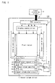
- FIG. 1 is a block diagram showing a schematic configuration of an active matrix substrate 100 included in the liquid crystal display device according to an embodiment of the present invention.
- the active matrix substrate 100 includes at least a pixel region 1, a display gate driver 2, a display source driver 3, a sensor column driver 4, a sensor row driver 5, a buffer amplifier 6, and an FPC connector 7 on a glass substrate.
- a signal processing circuit 8 for processing image signals picked up by a photodetection element (described later) in the pixel region 1 is connected to the active matrix substrate 100 via the FPC connector 7 and an FPC 9.
- the above constituent members on the active matrix substrate 100 can also be formed monolithically on the glass substrate by a semiconductor process.
- a configuration is possible in which the amplifier and various drivers among the above constituent members are mounted on the glass substrate by COG (Chip On Glass) technology or the like.
- COG Chip On Glass
- the active matrix substrate 100 is attached to a common substrate (not shown) that has a common electrode formed on the entire face thereof, and a liquid crystal material is enclosed in the gap therebetween.
- the pixel region 1 is a region in which a plurality of pixels are formed in order to display an image.
- a photosensor for picking up an image is provided in each pixel in the pixel region 1.
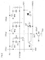
- FIG. 2 is an equivalent circuit diagram showing the disposition of a pixel and a photosensor in the pixel region 1 of the active matrix substrate 100.
- each pixel is formed by three colors of picture elements, namely R (red), G (green), and B (blue), and one photosensor is provided in each of the pixels composed of these three picture elements.
- the pixel region 1 has pixels disposed in a matrix having M rows ⁇ N columns, and photosensors that are likewise disposed in a matrix having M rows ⁇ N columns. Note that as described above, the number of picture elements is M ⁇ 3N.
- Thin-film transistors (TFTs) M1 are provided as switching elements for the pixels at intersections between the gate lines GL and the source lines COL.
- the thin-film transistors M1 provided in the red, green, and blue picture elements are designated by M1r, M1g, and M1b, respectively.
- the gate electrode is connected to one of the gate lines GL
- the source electrode is connected to one of the source lines COL
- the drain electrode is connected to a pixel electrode, which is not shown.
- a liquid crystal capacitor C LC is formed between the drain electrode of each thin-film transistor M1 and the common electrode (VCOM).
- an auxiliary capacitor C LS is formed between each drain electrode and a TFTCOM.
- the picture element driven by the thin-film transistor M1r which is connected to the intersection between one gate line GLi and one source line COLrj, is provided with a red color filter so as to correspond to that picture element, and red image data is supplied from the display source driver 3 to that picture element via the source line COLrj, and thus that picture element functions as a red picture element.
- the picture element driven by the thin-film transistor M1g which is connected to the intersection between the gate line GLi and the source line COLgj, is provided with a green color filter so as to correspond to that picture element, and green image data is supplied from the display source driver 3 to that picture element via the source line COLgj, and thus that picture element functions as a green picture element.
- the photosensors are provided in the ratio of one per pixel (three picture elements) in the pixel region 1.
- the disposition ratio of the pixels and photosensors is arbitrary and not limited to this example only.
- one photosensor may be disposed per picture element, and a configuration is possible in which one photosensor is disposed for a plurality of pixels.
- the photosensor incorporates a photodiode D1 serving as a photodetection element, a capacitor C1 (amplification element), and a thin-film transistor M2.
- the capacitor C1 that functions as an amplification element is a variable capacitor.
- the source line COLr also serves as wiring VDD, which is for supplying a constant voltage V DD from the sensor column driver 4 to the photosensor.
- the source line COLg also serves as wiring OUT for sensor output.
- the anode of the photodiode D1 is connected to wiring RST serving as reset signal wiring for supplying a reset signal.
- the cathode of the photodiode D1 is connected to one of the electrodes of the capacitor C 1 and the gate of the thin-film transistor M2.
- the drain of the thin-film transistor M2 is connected to the wiring VDD, and the source thereof is connected to the wiring OUT.
- the connection point (storage node) between the cathode of the photodiode D1, the one electrode of the capacitor C1, and the gate of the thin-film transistor M2 is designated by INT.
- the other electrode of the capacitor C1 is connected to wiring RWS serving as readout signal wiring for supplying a readout signal.
- the sensor row driver 5 successively selects a set of wiring RSTi and wiring RWSi shown in FIG. 2 at a predetermined time interval t row . Accordingly, each photosensor row in the pixel region 1 from which a signal charge is to be read out is successively selected.
- the end of the wiring OUT is connected to the drain of a thin-film transistor M3, which is an insulated gate field effect transistor. Also, the drain of this thin-film transistor M3 is connected to output wiring SOUT, and a potential V SOUT of the drain of the thin-film transistor M3 is output to the sensor column driver 4 as an output signal from the photosensor.
- the source of the thin-film transistor M3 is connected to the wiring VSS.
- the gate of the thin-film transistor M3 is connected to a reference voltage power supply (not shown) via reference voltage wiring VB.
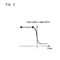
- FIG. 3 is a diagram showing CV characteristics of the capacitor C1.
- the horizontal axis indicates an interelectrode voltage V CAP of the capacitor C1
- the vertical axis indicates electrostatic capacitance.
- the capacitor C1 has a constant electrostatic capacitance while the interelectrode voltage V CAP is small
- the capacitor C1 has the characteristic that the electrostatic capacitance changes rapidly near the threshold of the interelectrode voltage V CAP . This enables dynamically changing the characteristics of the capacitor C1 using the potential of the readout signal from the wiring RWS.
- the photosensor of the present embodiment can amplify the change in the potential of the storage node in the integration period T INT when reading it out, as shown in FIG. 4 .
- the low level V RST.L of the reset signal is -1.4 volts
- the high level V RST.H of the reset signal is 0 volts.
- the low level V RWS.L of the readout signal is -3 volts
- the high level V RWS.H of the readout signal is 12 volts.
- the solid line waveform indicates changes in the potential V INT in the case where a small amount of light is incident on the photodiode D1
- the broken line waveform indicates changes in the potential V INT in the case where light at the saturation level has been incident on the photodiode D1
- ⁇ V SIG is the potential difference proportionate to the amount of light that has been incident on the photodiode D1.
- V INT V RSTH - V F
- V F is the forward voltage of the photodiode D1. Since V INT is lower than the threshold voltage of the thin-film transistor M2 at this time, the thin-film transistor M2 is in a non-conducting state in the reset period.
- the photocurrent integration period begins when the reset signal returns to the low level V RST.L .
- a photocurrent that is proportionate to the amount of light that has been incident on the photodiode D1 flows in the capacitor C1 to discharge the capacitor C1. Accordingly, the potential V INT of the connection point INT when the integration period T INT ends is expressed by Equation (5) below.
- V INT V RST . H - V F - ⁇ V RST ⁇ C PD / C T - I PHOTO ⁇ t INT / C T
- ⁇ V RST is the pulse height of the reset signal (V RST.H - V RST.L )
- I PHOTO is the photocurrent of the photodiode D1
- t INT is the length of the integration period.
- C PD is the capacitance of the photodiode D1.
- C TOTAL is the overall capacitance of the photosensor circuit, that is to say, the total capacitance of the connection point INT, which is the sum of the capacitance C INT of the capacitor C1, the capacitance C PD of the photodiode D1, and the capacitance C TFT of the thin-film transistor M2.
- V INT is lower than the threshold voltage of the thin-film transistor M2, and therefore the thin-film transistor M2 is in the non-conducting state.
- the readout signal supplied to the wiring RWS rises, and thus the readout period begins. At this point, the injection of charge into the capacitor C1 occurs. Then when the potential V INT of the connection point INT has become higher than the threshold voltage of the thin-film transistor M2, the thin-film transistor M2 enters a conductive state and functions as a source follower amplifier along with the bias thin-film transistor M3 provided at the end of the wiring OUT in each column.
- the output signal voltage from the output wiring SOUT from the drain of the thin-film transistor M3 corresponds to the amplified integral value of the photocurrent of the photodiode D1 in the integration period. The principles underlying this will be described later.
- operations are performed cyclically where one cycle involves initialization by a reset pulse, integration of the photocurrent in the integration period, and readout of sensor output in the readout period.
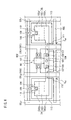
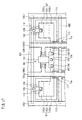
- the photosensor of the present embodiment includes the thin-film transistor M2 in the region between the source lines COLg and COLb.
- the photodiode D1 is a PIN diode having a lateral structure, in which a p-type semiconductor region 102p, an i-type semiconductor region 102i, and an n-type semiconductor region 102n are formed in series on a silicon film serving as the base.
- the p-type semiconductor region 102p serves as the anode of the photodiode D1, and is connected to the wiring RST via wiring 108 and contacts 109 and 110.
- the capacitor C1 is formed by a wide portion 111 formed in the wiring RWS, the extension portion 107 of the silicon film, and an insulating film (not shown) disposed therebetween.
- the wide portion 111 which has the same potential as the wiring RWS, functions as the gate electrode of the capacitor C1.
- a region 112 shown in FIG. 7 is a p+ region formed by doping an n-type silicon film with a p-type impurities such as boron.
- the extension portion 107 serves as a p+ region, and the portion of the silicon film below the wide portion 111 forms an n- region, as shown in FIG. 8 .
- FIG. 9 is a waveform diagram showing changes in the potential V INT of the storage node from the end of the integration period and throughout the readout period.
- a solid line waveform w1 indicates changes in the potential V INT in the case where a small amount of light is incident on the photodiode D1
- a broken line waveform w2 indicates changes in the potential V INT in the case where light has been incident on the photodiode D1.
- a time t 0 is the time when the readout signal supplied from the wiring RWS starts rising from the low level V RWS .
- a time t 2 is the time when the readout signal reaches the high level V RWS . H .
- a time t S is the time when the thin-film transistor M2 turns on and sampling of the sensor output is performed.
- a time t 1 is the time when the readout signal reaches a threshold voltage V off of the capacitor C1.
- the operation characteristics of the capacitor C1 change depending on the magnitude relationship between the potential supplied from the wiring RWS to the wide portion 111 and the threshold voltage V off .
- a time t 1 ' is the time when the readout signal reaches the threshold voltage V off of the capacitor C1 in the case of the waveform w2 (the case where light has been incident on the photodiode D1).
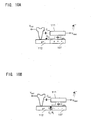
- FIGS. 10A and 10B are schematic cross-sectional diagrams showing differences in the movements of charge due to the potential of the gate electrode (wide portion 111) of the capacitor C1.
- the capacitor C1 is constantly on at times before time t 1 , and is off from t 1 onward.
- the potential of the wiring RWS is less than or equal to the threshold voltage V off
- movement of a charge Q inj occurs below the gate electrode (wide portion 111) as shown in FIG. 10A
- the potential of the wiring RWS exceeds the threshold voltage V off
- movement of the charge Q inj ceases to occur below the gate electrode (wide portion 111) as shown in FIG. 10B .
- H is as shown in Equation (6) below.
- ⁇ V INT shown in FIG. 4 corresponds to the difference between V INT (t 0 ) and V INT (t s ), and is equivalent to Q inj /C INT.
- V INT t s V INT t 0 + Q inj
- C INT C par + C gate
- C INT ⁇ ⁇ C par + C gate ⁇ C j C gate + C j
- ⁇ V SIG (t 0 ) at the end of the integration period is amplified to ⁇ V SIG (t 1 ). Accordingly, the potential difference at the storage node after the upthrust is greater than the potential difference at the storage node generated by the difference in illuminance on the light receiving face at the point in time when the integration period ends.
- the difference between the potential of the storage node after the upthrust in the readout period in the case of the dark condition and the potential of the storage node after the upthrust in the readout period in the case where light at the saturation level has been incident is greater than the difference between the potential of the storage node at the point in time when the storage period ends in the case of the dark condition and the potential of the storage node at the point in time when the storage period ends in the case where light at the saturation level has been incident.
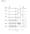
- the source lines COLr and COLg are also used as the photosensor wiring VDD and the photosensor wiring OUT, and therefore it is necessary to distinguish between times when image data signals for display are input via the source lines COLr, COLg, and COLb, and times when sensor output is read out, as shown in FIG. 11 .
- the reading out of the sensor output is performed using a horizontal blanking period or the like.
- HSYNC in FIG. 11 indicates a horizontal synchronization signal.
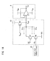
- the sensor column driver 4 includes a sensor pixel readout circuit 41, a sensor column amplifier 42, and a sensor column scan circuit 43.
- the sensor pixel readout circuit 41 is connected to the output wiring SOUT (see FIG. 2 ) that outputs the sensor output V SOUT from the pixel region 1.
- the sensor pixel readout circuit 41 outputs peak hold voltages V Sj of the sensor output V SOUTj to the sensor column amplifier 42.
- FIG. 12 is a circuit diagram showing the internal configuration of the sensor pixel readout circuit 41.
- FIG. 13 is a waveform diagram showing a relationship between the readout signal, sensor output, and output of the sensor pixel readout circuit.
- the output voltage Vs from the sensor pixel readout circuit 41 to the sensor column amplifier 42 is kept at the same level as the peak value of the sensor output V SOUT , as shown in FIG. 13 .
- each column amplifier is composed of thin-film transistors M6 and M7.
- the sensor column scan circuit 43 may scan the photosensor columns one column at a time as described above, there is no limitation to this, and a configuration is possible in which the photosensor columns are interlace-scanned. Also, the sensor column scan circuit 43 may be formed as a multi-phase drive scan circuit that has, for example, four phases.
- the display device of the present embodiment obtains panel output V OUT that is in accordance with the amount of light received by the photodiode D1 formed in each pixel in the pixel region 1.
- the panel output V OUT is sent to the signal processing circuit 8, subjected to A/D conversion, and then accumulated in a memory (not shown) as panel output data.
- the same number of panel output data pieces as the number of pixels (number of photosensors) in the pixel region 1 are accumulated in this memory.
- the signal processing circuit 8 performs various types of signal processing such as image pickup and the detection of a touch area.
- Embodiment 1 has the advantage that since the wide portion 111 of the wiring RWS also serves as the gate electrode of the capacitor C1, the number of contacts can be lower than, for example, that in the later-described Embodiment 3 (contacts 118 and 119 shown in FIG. 21 in Embodiment 3), thus enabling the size of the photosensor circuit to be reduced.
- the wide portion 111 of the wiring RWS is disposed so as to shield the storage node INT from the source line COL.
- Embodiment 2 of the present invention.
- Constituent elements having the same functions as constituent elements described in Embodiment 1 are given the same reference numerals as those in Embodiment 1, and detailed descriptions thereof will be omitted.
- FIG. 15 is an equivalent circuit diagram of the photosensor according to the present embodiment.
- FIG. 16 is a waveform diagram of a reset signal and a readout signal supplied to the photosensor according to the present embodiment.
- FIG. 17 is a plan view showing an example of a planar structure of the photosensor according to the present embodiment.
- FIG. 18 is an enlarged view of a region where the capacitor C1 is formed.
- FIG. 19 is a schematic cross-sectional diagram showing connection relationships between regions in the photosensor according to the present embodiment.
- the photosensor of the present embodiment differs from Embodiment 1 in that the capacitor C1 is an n-channel MOS capacitor. Also, the photodiode D1 is connected in the direction opposite that in Embodiment 1. Specifically, the cathode of the photodiode D1 is connected to the wiring RST, and the anode is connected to the storage node INT. Furthermore, the thin-film transistor M2 for readout is a p-channel TFT Also, as shown in FIG. 16 , the high level and low level potentials of the reset signal and the readout signal are reversed from those in Embodiment 1.
- the photodiode D1 is a PIN diode having a lateral structure, in which the p-type semiconductor region 102p, the i-type semiconductor region 102i, and the n-type semiconductor region 102n are formed in series on a silicon film serving as the base, similarly to Embodiment 1.
- the n-type semiconductor region 102n (cathode) is connected to the wiring RST via the wiring 108 and the contacts 109 and 110.
- the p-type semiconductor region 102p (anode) is connected to the gate electrode 101 of the thin-film transistor M2 via the extension portion 107 of the silicon film, the contacts 105 and 106, and the wiring 104.
- the capacitor C1 is formed by the wide portion 111 formed in the wiring RWS, the extension portion 107 of the silicon film, and an insulating film (not shown) disposed therebetween.
- the wide portion 111 which has the same potential as the wiring RWS, functions as the gate electrode of the capacitor C1.
- the region 112 shown in FIG. 18 is an n+ region formed by doping an n-type silicon film with n-type impurities such as phosphorus.
- the extension portion 107 serves as an n+ region, and the portion of the silicon film below the wide portion 111 forms an n-region, as shown in FIG. 19 .
- the change in the potential of the storage node V INT in the integration period and the readout period is the vertical opposite of that in FIG. 9 of Embodiment 1. Accordingly, with the photosensor of the present embodiment as well, the potential difference at the storage node after the upthrust is greater than the potential difference at the storage node generated by the difference in illuminance on the light receiving face at the point in time when the integration period ends.
- the difference between the potential of the storage node after the upthrust in the readout period in the case of the dark condition and the potential of the storage node after the upthrust in the readout period in the case where light at the saturation level has been incident is greater than the difference between the potential of the storage node at the point in time when the storage period ends in the case of the dark condition and the potential of the storage node at the point in time when the storage period ends in the case where light at the saturation level has been incident.
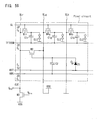
- FIG. 20 is an equivalent circuit diagram of the photosensor according to the present embodiment.
- FIG. 21 is a plan view showing an example of a planar structure of the photosensor according to the present embodiment.
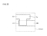
- FIG. 22 is an enlarged view of a region where the capacitor C1 is formed.
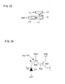
- FIG. 23 is a schematic cross-sectional diagram showing connection relationships between regions in the photosensor according to the present embodiment.
- the wiring from the gate electrode 101 of the thin-film transistor M2 extends to the region above the n-type semiconductor region 102n of the photodiode D1, and is connected to the n-type semiconductor region 102n via contacts 115 and 116.
- the wiring from the gate electrode 101 of the thin-film transistor M2 extends to the region over the capacitor C1 as well, and functions as a gate electrode 121 of the capacitor C1.
- the capacitor C1 is formed by the gate electrode 121, a silicon film 117, and an insulating film (not shown) disposed therebetween.
- the potential of the gate electrode 121 is the same as that of the storage node INT (V INT ).
- a region 112 shown in FIG. 22 is an n+ region formed by doping an n-type silicon film with n-type impurities such as phosphorus. Note that since the gate electrode 121 functions as a mask when doping with the n-type impurities is performed, the portion of the silicon film below the gate electrode 121 forms an n- region, as shown in FIG. 23 .
- the photosensor of the present embodiment is driven by the reset signal and the readout signal shown in FIG. 4 of Embodiment 1, and the changes in the potential of the storage node V INT in the integration period and the readout period are as shown in FIG. 9 of Embodiment 1. Accordingly, with the photosensor of the present embodiment as well, the potential difference of the storage node after the upthrust is greater than the potential difference of the storage node generated by the difference in illuminance on the light receiving face at the point in time when the integration period ends.
- the photosensor of the present embodiment also differs from Embodiment 1 in that the wide portion 111 of the wiring RWS extends to a position at which the entire width of the wiring 107 is covered. According to this configuration, the photosensor of the present embodiment has the advantage that the boundary length is shorter than that in the photosensor of Embodiment 1.
- the boundary length refers to the length of the boundary between the amplification element and the storage node INT.
- the capacitor C1 of Embodiment 1 is formed by the overlapping of the extension portion 107 of the silicon film and the wide portion 111 of the wiring RWS, as shown in FIGS. 6 and 7 .
- the boundary between the amplification element and the storage node INT is the portion where the outer edges of the wide portion 111 of the wiring RWS overlaps with the extension portion 107 of the silicon film, as shown by the bold line B.
- the boundary length is the sum of a length L CAP shown in FIG.
- the potential V INT of the storage node continues to rise in the period from time t 1 to time t 2 in which the readout signal rises, due to the parasitic capacitance between the amplification element and the storage node. Also, the potential V INT of the storage node continues to rise in the period from the time t 2 , at which the potential of the readout signal reached the high level V RWS.H , to the sampling time t S as well, due to leakage current. In this way, the rise in the potential V INT of the storage node from the time t 1 onward is not preferable since the potential amplification effect is reduced. It is preferable to shorten the boundary length of the amplification element in order to suppress the rise in the potential V INT attributed to the parasitic capacitance and leakage current from the time t 1 onward.
- the photosensor of Embodiment 4 has an advantage over the photosensor of Embodiment 1 in that since the boundary length of the amplification element is shorter, it is possible to suppress the rise in the potential V INT attributed to the parasitic capacitance and leakage current from the time t 1 onward.
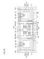
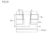
- the boundary length W TFT is further shortened while ensuring the effective area of the amplification element through a configuration in which, as shown in FIGS. 30 and 31 , the width of the extension portion 107 of the silicon film is shortened, and the extension portion 107 is provided with a wide portion 107a for ensuring the width W CAP of the amplification element.
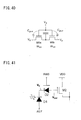
- FIG. 32 shows an equivalent circuit diagram of the p-channel TFT serving as the amplification element in this case.
- the boundary length can be shortened to a greater extent than in the configuration shown in FIGS. 24 to 28 , thus enabling further suppressing the rise in the potential V INT attributed to the parasitic capacitance and leakage current from the time t 1 onward. This enables realizing a photosensor with an even wider dynamic range.
- Embodiment 5 of the present invention. Constituent elements having the same functions as constituent elements described in the above embodiments are given the same reference numerals as those in the above embodiments, and detailed descriptions thereof will be omitted.
- an n-channel TFT (thin-film transistor M4) is used as the amplification element, in place of the n-channel MOS capacitor described in Embodiment 2.
- the drive signals of the photosensor of the present embodiment in which an n-channel TFT is used as the amplification element, have high level and low level potentials that are reversed from those of the drive signals in Embodiment 4, in which an n-channel TFT is used as the amplification element, as described in Embodiment 2 with reference to FIG. 16 .
- the potential V INT of the storage node can be amplified when being read out, as described with reference to FIG. 9 in Embodiment 1.
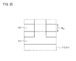
- the photosensor of the present embodiment differs from Embodiment 2 in that the wide portion 111 of the wiring RWS extends to a position at which the entire width of the wiring 107 is covered.
- the photosensor of the present embodiment has the advantage that the boundary length is shorter than that in the photosensor of Embodiment 2.
- the boundary length of the photosensor of Embodiment 2 is L CAP + 2 ⁇ W CAP as shown in FIG. 18 .
- the boundary length of the photosensor of the present embodiment is the width W TFT of the extension portion 107 as shown in FIG. 35 .
- FIG. 40 shows an equivalent circuit diagram of the n-channel TFT serving as the amplification element in this case.
- the boundary length can be shortened to a greater extent than in the configuration shown in FIGS. 33 to 37 , thus enabling further suppressing the rise in the potential V INT attributed to the parasitic capacitance and leakage current from the time t 1 onward. This enables realizing a photosensor with an even wider dynamic range.
- FIG. 41 is an equivalent circuit diagram of the photosensor according to the present embodiment.
- FIG. 42 is a plan view showing an example of a planar structure of the photosensor according to the present embodiment.
- FIG. 43 is an enlarged view of a region where an amplification element (photodiode D2) is formed.
- FIG. 44 is a schematic cross-sectional diagram showing connection relationships between regions in the photosensor according to the present embodiment.
- FIG. 45 is an equivalent circuit diagram of the photodiode serving as the amplification element.
- FIG. 46 is an equivalent circuit diagram of a photosensor according to a first variation of the present embodiment.
- FIG. 47 is a plan view showing an example of a planar structure of the photosensor according to the first variation.
- the photosensor of the first variation of the present embodiment has a configuration including an additional thin-film transistor M5 for resetting.
- Embodiment 7 of the present invention Constituent elements having the same functions as constituent elements described in the above embodiments are given the same reference numerals as those in the above embodiments, and detailed descriptions thereof will be omitted.
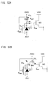
- FIG. 50 is an equivalent circuit diagram of the photosensor according to the present embodiment.
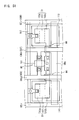
- FIG. 51 is a plan view showing an example of a planar structure of the photosensor according to the present embodiment.
- the photosensor of the present embodiment has the configuration shown in FIGS. 30 to 32 in Embodiment 4, in which the light shielding film 113 provided on the back face of the photodiode D1 has been extended to a position opposing the wiring RWS, and a capacitor C SER is formed by the light shielding film 113, the wiring RWS, and an insulating film (not shown) therebetween, as shown in FIGS. 50 and 51 .
- the photosensor of the present embodiment uses a p-channel TFT (thin film transistor M4) as the amplification element, similarly to Embodiment 4.
- the capacitor C SER functions as a series capacitor in series with capacitors Cc and Ca between the light shielding film 113 and the photodiode D1. This enables increasing only C INT , without increasing C INT ', in Equation (6) described in Embodiment 1, thus enabling improving the amplification effect during readout.
- the potential V INT of the storage node during readout is influenced by not only a charge ⁇ Q C from the capacitor C1, but also a charge Qs injected from the capacitor C SER . Accordingly, in this configuration, the existence of the capacitor C SER reduces the amplification effect during readout.
- a photosensor in which the capacitor C SER is combined with a configuration using a p-channel TFT as the amplification element, as in the present embodiment, is effective in terms of obtaining a high amplification effect.
- FIG. 53 is an equivalent circuit diagram of the photosensor according to the present embodiment.
- FIG. 54 is a plan view showing an example of a planar structure of the photosensor according to the present embodiment.
- photodiodes D1 and capacitors C3 are formed in parallel across a plurality of pixel regions.
- Each capacitor C3 is a normal (not variable) capacitor. Note that although the example of a configuration in which one thin-film transistor M2 for readout is used to read out four photodiodes D1 is shown in FIGS. 53 and 54 , the number of photodiodes D1 to be read out is not limited to this.
- the p-channel TFT (thin-film transistor M4) in the pixel region closest to the transistor M2 for readout is formed as an amplification element, and a normal (not variable) capacitor C3 is formed in the other pixel regions.
- the photocurrent can be increased by connecting multiple photodiodes D1 in parallel. Also, disposing the amplification element in the region including the photodiode D 1 closest to the thin-film transistor M2 for readout enables the potential of the storage node to be amplified when being read out. This enables realizing a highly sensitive photosensor without deterioration of the S/N ratio. Also, using a p-channel TFT as the amplification element enables setting the boundary length shorter than in the case of using a variable capacitor, as previously described. This enables further improving the amplification effect.
- Embodiment 9 of the present invention. Constituent elements having the same functions as constituent elements described in the above embodiments are given the same reference numerals as those in the above embodiments, and detailed descriptions thereof will be omitted.
- FIG. 55 is an equivalent circuit diagram of the photosensor according to the present embodiment.
- FIG. 56 is a plan view showing an example of a planar structure of the photosensor according to the present embodiment.
- photodiodes D1 and capacitors C3 are formed in parallel across a plurality of pixel regions.
- Each capacitor C3 is a normal (not variable) capacitor. Note that although the example of a configuration in which one thin-film transistor M2 for readout is used to read out four photodiodes D 1 is shown in FIGS. 55 and 56 , the number of photodiodes D1 to be read out is not limited to this.
- a photodiode D2 is provided as an amplification element in the pixel region including, among the four photodiodes D1, the photodiode D1 closest to the thin-film transistor M2 for readout, and the normal (not variable) capacitors C3 are formed in the other pixel regions. Also, a thin-film transistor M5 for resetting is formed in the pixel region adjacent to the thin-film transistor M2 for readout.
- the photocurrent can be increased by connecting multiple photodiodes D1 in parallel. Also, disposing the amplification element (photodiode D2) in the region including the photodiode D1 closest to the thin-film transistor M2 for readout enables the potential of the storage node to be amplified when being read out. This enables realizing a highly sensitive photosensor without deterioration of the S/N ratio. Also, using the photodiode D2 as the amplification element enables setting the boundary length shorter than in the case of using a variable capacitor, as previously described. This enables further improving the amplification effect.
- Embodiment 10 of the present invention Constituent elements having the same functions as constituent elements described in the above embodiments are given the same reference numerals as those in the above embodiments, and detailed descriptions thereof will be omitted.
- FIG. 57 is an equivalent circuit diagram of the photosensor according to the present embodiment.
- FIG. 58 is a plan view showing an example of a planar structure of the photosensor according to the present embodiment.
- the photosensor of the present embodiment has the configuration of the photosensor of embodiment 1 with an additional thin-film transistor M5 for resetting.
- the gate electrode 131 of the thin-film transistor M5 for resetting extends out from the wiring RST.
- the potential of the storage node can be amplified when being read out, similarly to the photosensor of Embodiment 1. This enables realizing a highly sensitive photosensor without deterioration of the S/N ratio.
- Embodiment 1 the configuration in which the thin-film transistor M5 for resetting is provided in this way can be applied to Embodiment 2, Embodiment 3, Embodiment 4, Embodiment 5, Embodiment 7, and Embodiment 8 as well, thus achieving the effects described in the respective embodiments.
- the present invention is industrially applicable as a display device having a photosensor in a pixel region of an active matrix substrate.
Landscapes
- Engineering & Computer Science (AREA)
- Theoretical Computer Science (AREA)
- General Engineering & Computer Science (AREA)
- Physics & Mathematics (AREA)
- General Physics & Mathematics (AREA)
- Human Computer Interaction (AREA)
- Chemical & Material Sciences (AREA)
- Crystallography & Structural Chemistry (AREA)
- Computer Hardware Design (AREA)
- Liquid Crystal (AREA)
- Solid State Image Pick-Up Elements (AREA)
- Devices For Indicating Variable Information By Combining Individual Elements (AREA)
- Control Of Indicators Other Than Cathode Ray Tubes (AREA)
- Transforming Light Signals Into Electric Signals (AREA)
Applications Claiming Priority (2)
| Application Number | Priority Date | Filing Date | Title |
|---|---|---|---|
| JP2009048400 | 2009-03-02 | ||
| PCT/JP2010/050078 WO2010100958A1 (ja) | 2009-03-02 | 2010-01-07 | 表示装置 |
Publications (2)
| Publication Number | Publication Date |
|---|---|
| EP2392964A1 true EP2392964A1 (de) | 2011-12-07 |
| EP2392964A4 EP2392964A4 (de) | 2013-06-05 |
Family
ID=42709523
Family Applications (1)
| Application Number | Title | Priority Date | Filing Date |
|---|---|---|---|
| EP10748556.7A Withdrawn EP2392964A4 (de) | 2009-03-02 | 2010-01-07 | Anzeigevorrichtung |
Country Status (6)
| Country | Link |
|---|---|
| US (1) | US8772699B2 (de) |
| EP (1) | EP2392964A4 (de) |
| JP (1) | JP5421355B2 (de) |
| CN (1) | CN102341749B (de) |
| RU (1) | RU2011139956A (de) |
| WO (1) | WO2010100958A1 (de) |
Families Citing this family (5)
| Publication number | Priority date | Publication date | Assignee | Title |
|---|---|---|---|---|
| CN103959363B (zh) * | 2011-12-07 | 2016-04-27 | 夏普株式会社 | 光传感器电路的动作方法、以及具备该光传感器电路的显示装置的动作方法 |
| US9106191B2 (en) * | 2012-05-02 | 2015-08-11 | Adaptive I/O Technologies, Inc. | Diode enhanced amplifier circuits and methods thereof |
| CN104282628B (zh) * | 2014-10-29 | 2017-12-08 | 上海集成电路研发中心有限公司 | 一种cmos图像传感器全局像元存储电容的制作方法 |
| CN108320690B (zh) * | 2018-02-01 | 2021-04-09 | 京东方科技集团股份有限公司 | 显示面板及其检测方法、显示装置 |
| CN115482785A (zh) * | 2022-09-15 | 2022-12-16 | 京东方科技集团股份有限公司 | 显示装置、显示方法以及电子设备 |
Family Cites Families (13)
| Publication number | Priority date | Publication date | Assignee | Title |
|---|---|---|---|---|
| US5898207A (en) * | 1996-02-13 | 1999-04-27 | Matsushita Electric Industrial Co., Ltd. | Method for making a semiconductor device |
| JP4737956B2 (ja) | 2003-08-25 | 2011-08-03 | 東芝モバイルディスプレイ株式会社 | 表示装置および光電変換素子 |
| KR100669270B1 (ko) | 2003-08-25 | 2007-01-16 | 도시바 마쯔시따 디스플레이 테크놀로지 컴퍼니, 리미티드 | 표시 장치 및 광전 변환 소자 |
| JP4055722B2 (ja) * | 2003-11-10 | 2008-03-05 | ソニー株式会社 | アクティブマトリクス型有機el表示装置 |
| US7423790B2 (en) * | 2004-03-18 | 2008-09-09 | Canon Kabushiki Kaisha | Photoelectric conversion apparatus and contact-type image sensor |
| GB2439118A (en) | 2006-06-12 | 2007-12-19 | Sharp Kk | Image sensor and display |
| GB2439098A (en) | 2006-06-12 | 2007-12-19 | Sharp Kk | Image sensor and display |
| JP2008153427A (ja) * | 2006-12-18 | 2008-07-03 | Hitachi Displays Ltd | 高感度光センサ素子及びそれを用いた光センサ装置 |
| GB2446821A (en) * | 2007-02-07 | 2008-08-27 | Sharp Kk | An ambient light sensing system |
| JP4793281B2 (ja) | 2007-02-21 | 2011-10-12 | ソニー株式会社 | 撮像装置および表示装置 |
| CN101636644B (zh) * | 2007-04-09 | 2011-08-31 | 夏普株式会社 | 显示装置 |
| JP5058256B2 (ja) | 2007-06-21 | 2012-10-24 | シャープ株式会社 | 光検出装置、及びそれを備えた表示装置 |
| US8350835B2 (en) | 2007-08-21 | 2013-01-08 | Sharp Kabushiki Kaisha | Display device |
-
2010
- 2010-01-07 JP JP2011502676A patent/JP5421355B2/ja not_active Expired - Fee Related
- 2010-01-07 US US13/254,422 patent/US8772699B2/en active Active
- 2010-01-07 CN CN201080009924.8A patent/CN102341749B/zh not_active Expired - Fee Related
- 2010-01-07 RU RU2011139956/28A patent/RU2011139956A/ru unknown
- 2010-01-07 WO PCT/JP2010/050078 patent/WO2010100958A1/ja not_active Ceased
- 2010-01-07 EP EP10748556.7A patent/EP2392964A4/de not_active Withdrawn
Also Published As
| Publication number | Publication date |
|---|---|
| CN102341749B (zh) | 2015-02-25 |
| RU2011139956A (ru) | 2013-04-10 |
| WO2010100958A1 (ja) | 2010-09-10 |
| US20110315860A1 (en) | 2011-12-29 |
| JP5421355B2 (ja) | 2014-02-19 |
| US8772699B2 (en) | 2014-07-08 |
| JPWO2010100958A1 (ja) | 2012-09-06 |
| EP2392964A4 (de) | 2013-06-05 |
| CN102341749A (zh) | 2012-02-01 |
Similar Documents
| Publication | Publication Date | Title |
|---|---|---|
| US8350835B2 (en) | Display device | |
| US8759739B2 (en) | Optical sensor and display apparatus | |
| US20110080391A1 (en) | Display device | |
| JP5284487B2 (ja) | 表示装置 | |
| EP2287657A1 (de) | Anzeigevorrichtung | |
| WO2009148084A1 (ja) | 表示装置 | |
| US20130063403A1 (en) | Display device with touch sensor | |
| EP2472854A1 (de) | Lichtsensor und anzeigevorrichtung | |
| US8427464B2 (en) | Display device | |
| US20110315859A1 (en) | Display device | |
| WO2010092709A1 (ja) | 表示装置 | |
| US8772699B2 (en) | Display device having a photosensor | |
| US20110096049A1 (en) | Display device | |
| US20110102393A1 (en) | Display device | |
| CN101622658B (zh) | 液晶显示装置 | |
| US20130057527A1 (en) | Display device |
Legal Events
| Date | Code | Title | Description |
|---|---|---|---|
| PUAI | Public reference made under article 153(3) epc to a published international application that has entered the european phase |
Free format text: ORIGINAL CODE: 0009012 |
|
| 17P | Request for examination filed |
Effective date: 20110831 |
|
| AK | Designated contracting states |
Kind code of ref document: A1 Designated state(s): AT BE BG CH CY CZ DE DK EE ES FI FR GB GR HR HU IE IS IT LI LT LU LV MC MK MT NL NO PL PT RO SE SI SK SM TR |
|
| DAX | Request for extension of the european patent (deleted) | ||
| A4 | Supplementary search report drawn up and despatched |
Effective date: 20130508 |
|
| RIC1 | Information provided on ipc code assigned before grant |
Ipc: G06F 3/042 20060101ALI20130502BHEP Ipc: H04N 5/335 20110101ALI20130502BHEP Ipc: G09F 9/30 20060101ALI20130502BHEP Ipc: G02F 1/1333 20060101ALI20130502BHEP Ipc: G02F 1/1368 20060101AFI20130502BHEP Ipc: G02F 1/133 20060101ALI20130502BHEP |
|
| STAA | Information on the status of an ep patent application or granted ep patent |
Free format text: STATUS: THE APPLICATION HAS BEEN WITHDRAWN |
|
| 18W | Application withdrawn |
Effective date: 20131108 |