EP2387151A1 - Millimeter-wave switches and attenuators - Google Patents
Millimeter-wave switches and attenuators Download PDFInfo
- Publication number
- EP2387151A1 EP2387151A1 EP10005689A EP10005689A EP2387151A1 EP 2387151 A1 EP2387151 A1 EP 2387151A1 EP 10005689 A EP10005689 A EP 10005689A EP 10005689 A EP10005689 A EP 10005689A EP 2387151 A1 EP2387151 A1 EP 2387151A1
- Authority
- EP
- European Patent Office
- Prior art keywords
- coupled
- terminal
- node
- bipolar transistor
- capacitor
- Prior art date
- Legal status (The legal status is an assumption and is not a legal conclusion. Google has not performed a legal analysis and makes no representation as to the accuracy of the status listed.)
- Granted
Links
Images



Classifications
-
- H—ELECTRICITY
- H03—ELECTRONIC CIRCUITRY
- H03H—IMPEDANCE NETWORKS, e.g. RESONANT CIRCUITS; RESONATORS
- H03H7/00—Multiple-port networks comprising only passive electrical elements as network components
- H03H7/24—Frequency- independent attenuators
- H03H7/25—Frequency- independent attenuators comprising an element controlled by an electric or magnetic variable
-
- H—ELECTRICITY
- H04—ELECTRIC COMMUNICATION TECHNIQUE
- H04B—TRANSMISSION
- H04B1/00—Details of transmission systems, not covered by a single one of groups H04B3/00 - H04B13/00; Details of transmission systems not characterised by the medium used for transmission
- H04B1/38—Transceivers, i.e. devices in which transmitter and receiver form a structural unit and in which at least one part is used for functions of transmitting and receiving
- H04B1/40—Circuits
-
- H—ELECTRICITY
- H01—ELECTRIC ELEMENTS
- H01P—WAVEGUIDES; RESONATORS, LINES, OR OTHER DEVICES OF THE WAVEGUIDE TYPE
- H01P1/00—Auxiliary devices
- H01P1/10—Auxiliary devices for switching or interrupting
- H01P1/15—Auxiliary devices for switching or interrupting by semiconductor devices
Definitions
- the present invention relates to an mm Wave attenuator according to the pre-characterizing clause of claim 1.
- While switches are straightforward to implement on a silicon IC (integrated circuit) at low-to-moderate frequencies, the implementation becomes increasingly difficult at millimeter-wave (mm Wave) frequencies, because of losses caused by undesired parasitic circuit capacitance (C), resistance (R), and inductance (L).
- C parasitic circuit capacitance
- R resistance
- L inductance
- series switches become lossy at mm Wave frequencies, and a variety of circuits have been invented to reduce the loss of series switches.
- Shunt switch topologies can be less lossy at high frequencies, but the performance of even shunt topologies is ultimately limited by the on-state R and off-state RCL of the shunt switching element.
- the related arts fail to overcome the problem of providing an effective switch (or switchable attenuator) on a silicon integrated circuit (IC) at millimeter-wave frequencies, which has the desired isolation or attenuation, while also providing very low insertion loss when no attenuation is desired.
- the present invention aims at providing an mm Wave attenuator that has the desired isolation or attenuation, while also providing very low insertion loss when no attenuation is desired.
- the claimed mm Wave attenuator includes a switchable attenuator on a silicon integrated circuit at millimeter-wave frequencies that has serially coupled shunt structures.
- This disclosure presents several new shunt switching circuits which provide good performance, even at mm Wave frequencies. These circuits may be implemented in a SiGe BiCMOS technology, but in some cases also may be implemented in Si CMOS or other IC technologies.
- the switchable input attenuator 12 may be implemented as part of a mixer 10, e.g., an RF-to-IF mixer in an mm Wave receiver.
- the mixer 10 may have signal processing capability and may be included in an RF receiver section of communication devices, such as cellular telephones.
- the disclosed techniques can also be used for both IC level design and printed circuit board (PCB) level designs to reduce noise coupling, chip area, power consumption and the number of components employed in a circuit.
- This mixer 10 accepts a very wide range of input signal powers, up to +5 dBm, and has a wide range of selectable gains.
- input signal powers up to approximately -4 dBm can be accommodated in a straightforward way.
- a double-balanced mixer with a differential, common-base input which has an iCP1dB of -4 dBm may be used.
- Input signal powers > -4 dBm are most readily accommodated using an adjustable input attenuator.
- the input attenuator may be linear at signal levels of +5 dBm and also preferably have low loss when in the off (e.g., non-attenuating) state.
- the input attenuator may also preserve an accurate 50 ⁇ single-ended (100 ⁇ differential) input match in both on and off states.
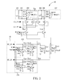
- the input attenuator 12 is shown conceptually in FIG.1 , which is a simplified schematic of the receiver RF-to-IF mixer 10 where the input attenuator 12 is within the dashed box.
- the RF-to-IF mixer 10 may include several parallel circuits such as a first parallel circuit 101 that may have a first terminal of an inductor L 1 coupled with a supplied voltage Vcc and a second terminal of first inductor L1 coupled with both a first terminal of a bipolar transistor Q3 and with a first terminal of a bipolar transistor Q5.
- a second parallel circuit 102 may have a first terminal of a capacitor C1 coupled with the supplied voltage Vcc and a second terminal of the capacitor C1 coupled with both the first terminal of the bipolar transistor Q3 and the first terminal of the bipolar transistor Q5.
- a third parallel circuit 103 may comprise a plurality of resisters R1C, R1B, and R1A coupled in a first series, with a first terminal of the first series coupled with the supplied voltage Vcc and a second terminal of the first series coupled with both the first terminal of bipolar transistor Q3 and the first terminal of bipolar transistor Q5.
- a first multiplexer MUX1 may select for output OUT+ from voltages occurring at a node between R1C and R1B, at a node between R1B and R1A, or at a node between R1A and the first terminal of bipolar transistor Q3.
- a fourth parallel circuit 105 may have a first terminal of a second inductor L2 coupled with the supplied voltage Vcc and a second terminal of the inductor L2 coupled with both a first terminal of a bipolar transistor Q4 and with a first terminal of a bipolar transistor Q6.
- a fifth parallel circuit 106 may have a first terminal of a capacitor C2 coupled with the supplied voltage Vcc and a second terminal of the capacitor C2 coupled with both the first terminal of the bipolar transistor Q4 and the first terminal of the bipolar transistor Q4.
- a sixth parallel circuit 107 may comprise a plurality of resisters R2C, R2B, and R2A coupled in a second series, with a first terminal of the second series coupled with the supplied voltage Vcc and a second terminal of the second series coupled with both the first terminal of bipolar transistor Q4 and the first terminal of bipolar transistor Q6.
- a second multiplexer MUX2 may select for output OUT- from voltages occurring at a node between R2C and R2B, at a node between R2B and R2A, or at a node between R2A and the first terminal of bipolar transistor Q4.
- Control terminals of both the bipolar transistor Q3 and the bipolar transistor Q6 may be coupled to receive input signal LO_IN+ and control terminals of both the bipolar transistor Q4 and the bipolar transistor Q5 may be coupled to receive input signal LO_IN-.
- a first transmission line TLc1 may couple a first terminal of a bipolar transistor Q1 with a second terminal of the bipolar transistor Q3 and a second terminal of the bipolar transistor Q4.
- a second transmission line TLc2 may couple a first terminal of a bipolar transistor Q2 with a second terminal of the bipolar transistor Q5 and a second terminal of the bipolar transistor Q6.
- Control terminals of both the bipolar transistor Q1 and the bipolar transistor Q2 may be coupled to receive an input BIAS signal; the input BIAS signal also may be coupled to ground via a capacitor Cbyp3.
- a second terminal of the bipolar transistor Q1 may be coupled to the input attenuator 12 via a transmission line TL1, to ground via a capacitor Ce1, and to a first terminal of a transmission line TLe1.
- a second terminal of the transmission line TLe1 may be coupled to ground via a capacitor Cbyp1 and to ground via a resistor Re1.
- a second terminal of the bipolar transistor Q2 may be coupled to the input attenuator 12 via a transmission line TL2, to ground via a capacitor Ce2, and to a first terminal of a transmission line TLe2.
- a second terminal of the transmission line TLe2 may be coupled to ground via a capacitor Cbyp2 and to ground via a resistor Re2.
- the input attenuator 12 of the mixer 10 may comprise two parallel input circuits.
- the first parallel input circuit 115 may be coupled to receive input signal RF_IN+ for transmission of the input signal RF_IN+ to the transmission line TL1 via a transmission line TL3 and a DC blocking capacitor Cb13 coupled in series.
- a node on the transmission line TL3 between the RF_IN+ input terminal and the capacitor Cb13 may be selectively coupled to ground via a capacitor Cm3 and a switch Sw3 according to the setting of the switch Sw3.
- a first node between the capacitor Cb13 and the transmission line TL1 may be coupled to ground via a capacitor Cm1 and a second node between the capacitor Cb13 and the transmission line TL1 may be selectively coupled to ground via a DC blocking capacitor Cb11, a resistor Ratt1, and a switch Sw1 according to the setting of the switch Sw1.
- the second parallel input circuit 116 may be coupled to receive input signal RF_IN- for transmission of the input signal RF_IN- to the transmission line TL2 via a transmission line TL4 and a DC blocking capacitor Cb14 coupled in series.
- a node on the transmission line TL4 between the RF_IN- input terminal and the capacitor Cb14 may be selectively coupled to ground via a capacitor Cm4 and a switch Sw4 according to setting of the switch Sw4.
- a first node between the capacitor Cb14 and the transmission line TL2 may be coupled to ground via a capacitor Cm2 and a second node between the capacitor Cm2and the transmission line TL2 may be selectively coupled to ground via a DC blocking capacitor Cb12, a resistor Ratt2, and a switch Sw2 according to the setting of the switch Sw2.
- Transmission line TL1 and capacitor Cm1 can match the input of the mixer 10 to typically 50 ⁇ single-ended.
- transmission line TL2 and capacitor Cm2 can match the other input of the mixer 10 to typically 50 ⁇ single-ended.
- Capacitors Cb13 and Cb14 may be DC-blocking capacitors.
- Transmission lines TL3 and TL4 may be designed with a characteristic impedance of 50 ⁇ , or whatever impedance the input of the mixer 10 is matched to. When the input attenuator 12 is off, transmission lines TL3 and TL4 do not significantly affect the mixer input impedance.
- FIG.2 details one embodiment of a mixer 20 that may include first, second, third, fourth, fifth, and sixth parallel circuits 201, 202, 203, 205, 206 and 207 respectively corresponding to the first , second, third, fourth, fifth, and sixth parallel circuits 101, 102, 103, 105, 106, and 107 of FIG.1 as well as other components sharing the same labels.
- the switches SW1-SW4 of the switchable attenuator 12 of FIG.1 are implemented as bipolar transistors Q7-Q10 in the switchable attenuator 22.
- the switchable attenuator 22 over the switchable attenuator 12 include a first input line receiving a bias voltage VC as input and a second input line receiving a control signal VSW.
- the first input line may couple bias voltage VC to a first terminal of the bipolar transistor Q7 via a resistor Rc7, bias voltage VC to a first terminal of the bipolar transistor Q9 via a resistor Rc9, bias voltage VC to a first terminal of the bipolar transistor Q8 via a resistor Rc8, and bias voltage VC to a first terminal of the bipolar transistor Q10 via a resistor Rc10.
- the second input line may couple a control signal VSW to a control terminal of the bipolar transistor Q7 via a resistor Rb7, the control signal VSW to a control terminal of the bipolar transistor Q9 via a resistor Rb9, the control signal VSW to a control terminal of the bipolar transistor Q8 via a resistor Rb8, and the control signal VSW to a control terminal of the bipolar transistor Q10 via a resistor Rb10.
- the control terminal of the bipolar transistor Q7 may also be coupled to ground via a capacitor Cb7
- the control terminal of the bipolar transistor Q9 may also be coupled to ground via a capacitor Cb9
- the control terminal of the bipolar transistor Q8 may also be coupled to ground via a capacitor Cb8
- the control terminal of the bipolar transistor Q10 may also be coupled to ground via a capacitor Cb10.
- bipolar transistors Q7-Q10 When the control signal VSW is high, bipolar transistors Q7-Q10 are on in a saturated state.
- the on-state AC resistance of bipolar transistor Q7 in series with resistor Ratt1 (and bipolar transistor Q8 in series with resistor Ratt2) may be chosen to be 15 ⁇ , or whatever value gives the desired attenuation. Higher base current in bipolar transistors Q7-Q10 forces the bipolar transistors Q7-Q10 deeper into saturation and reduces the on-state resistance.
- Bipolar transistors Q9 and Q10 could have on-state resistance which is small compared to the impedance of capacitors Cm3 and Cm4 at 60GHz (or whatever the operating frequency is).
- bipolar transistors Q7-Q10 when the control signal VSW is low, bipolar transistors Q7-Q10 are off. Their off-state capacitance could be low compared to other capacitances in the circuit, such as capacitors Cm1-Cm2.
- a bias voltage VC is applied to the collectors of bipolar transistors Q7-Q10 through large resistors Rc7-Rc10 to prevent the large AC signal swings from forward biasing the base-collector junctions when the bipolar transistors Q7-Q10 are in the off-state.
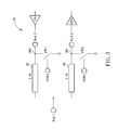
- a second example of a shunt switching circuit is a millimeter-wave transmit/receive (T/R) switch is shown in FIG. 3 .
- the millimeter-wave T/R switch is a highly desired circuit block for cost and complexity reduction in the 60GHz radio application. The most common application is to facilitate antenna sharing between transmitter and receiver. Another application of the same switch topology is in discrete phase-shifters. In both cases, the switch has low on-state insertion-loss to minimize its impact on the system link budget.
- a shunt switching circuit 30 may comprise a first circuit having Port 1 terminal, a first 1/4 wave transmission line 32, a first node 302, and a Port 2 terminal coupled in series.
- a switch SW1 controlled by a control signal VSW1 couples or decouples the first node 302 with ground.
- the Port 2 terminal may receive input from a power amplifier PA.
- the shunt switching circuit 30 may further comprise a second circuit parallel to the first circuit having the Port 1 terminal, a second 1/4 wave transmission line 34, a second node 304, and a Port 3 terminal coupled in series.
- a switch SW2 controlled by a control signal VSW2 couples or decouples the second node 304 with ground.
- the Port 3 terminal may output to a low noise amplifier LNA.
- the lowest loss T/R switch topology is one without a series element, as in FIG.3 .
- the switch SW1 is closed and the switch SW2 is opened.
- the switch SW1 is closed, a short is created at Port 2 and the transmission line TL2 transforms the short into an open at Port 1.
- a variation on this switch is a variable attenuator whereby the signal passed from Port 1 to Port 3 is attenuated when the switch SW2 is partially on.
- T/R switch may require a semiconductor device with ideal switching characteristics, and hence has traditionally been implemented with MOSFETs.
- MOSFETs display several disadvantages that make them less suitable for the 60GHz application:
- SiGe HBTs silicon germanium heterojunction bipolar transistor
- FIG. 5 The implementation of the basic SiGe HBT switching device 50 is illustrated in FIG. 5 . Note that this is a similar implementation as in FIG.2 (RF-attenuator utilized in the mixer).
- the control signal VSW is used to vary the on-state resistance of the switch. Referring to FIG. 5 :
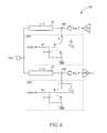
- FIG.6 shows how the switch elements of FIG.5 are used to build a T/R switch 50.
- SW1 and SW2 of FIG.6 each comprise a SiGe HBT as shown.
- Each SiGe HBT receives a control signal (the switch SW1 receives the control signal VSW1, and the switch SW2 receives the control signal VSW2) which is respectively routed through a resistor R1 to a control terminal B and also through a capacitor C1 to the emitter terminal E and VBB of each SiGe HBT.
- the collector C of the SiGe HBT of the switch SW1 is coupled to a first node 602 between the first 1/4 wave transmission line 62 and Port 2 terminal.
- the collector C of the SiGe HBT of the switch SW2 is coupled to a second node 604 between the second 1/4 wave transmission line 64 and Port 3 terminal. Because one switch element is always on, the collector bias voltage of both switch elements is always 1.25V, which is the optimum large-signal bias for the switch in the off state.
- Any signal swing present at the collector of the on-state switch causes the region of operation of the on-state switch to move between the forward and reverse saturation modes, as shown in FIG.7 .
- the circuits presented within this disclosure represent new and effective switching in mm Wave frequencies.
- the use of properly biased silicon germanium heterojunction bipolar transistors as disclosed is highly advantageous, and provides an effective switch (or switchable attenuator) on a silicon integrated circuit (IC) at millimeter-wave frequencies, which has the desired isolation or attenuation, while also providing very low insertion loss when no attenuation is desired.
Landscapes
- Engineering & Computer Science (AREA)
- Computer Networks & Wireless Communication (AREA)
- Signal Processing (AREA)
- Networks Using Active Elements (AREA)
- Attenuators (AREA)
- Electronic Switches (AREA)
- Control Of Amplification And Gain Control (AREA)
- Amplifiers (AREA)
Abstract
Description
- The present invention relates to an mm Wave attenuator according to the pre-characterizing clause of
claim 1. - While switches are straightforward to implement on a silicon IC (integrated circuit) at low-to-moderate frequencies, the implementation becomes increasingly difficult at millimeter-wave (mm Wave) frequencies, because of losses caused by undesired parasitic circuit capacitance (C), resistance (R), and inductance (L).
- In particular, series switches become lossy at mm Wave frequencies, and a variety of circuits have been invented to reduce the loss of series switches. Shunt switch topologies can be less lossy at high frequencies, but the performance of even shunt topologies is ultimately limited by the on-state R and off-state RCL of the shunt switching element.
- However, the related arts fail to overcome the problem of providing an effective switch (or switchable attenuator) on a silicon integrated circuit (IC) at millimeter-wave frequencies, which has the desired isolation or attenuation, while also providing very low insertion loss when no attenuation is desired.
- This in mind, the present invention aims at providing an mm Wave attenuator that has the desired isolation or attenuation, while also providing very low insertion loss when no attenuation is desired.
- This is achieved by an mm Wave attenuator according to
claim 1. The dependent claims pertain to corresponding further developments and improvements. - As will be seen more clearly from the detailed description following below, the claimed mm Wave attenuator includes a switchable attenuator on a silicon integrated circuit at millimeter-wave frequencies that has serially coupled shunt structures.
- In the following, the invention is further illustrated by way of example, taking reference to the accompanying drawings. Thereof
-
FIG. 1 is an input attenuator according to one embodiment of the disclosure. -
FIG.2 details one embodiment of a mixer where the switches SW1-SW4 of FIG. are implemented as bipolar transistors. -
FIG.3 illustrates second example of a shunt switching circuit in a millimeter-wave transmit/receive switch. -
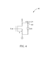
FIG.4 illustrates a MOSFET switch in its off-state driven by a power amplifier. -
FIG.5 illustrates an implementation of a basic SiGe HBT switching device. -
FIG.6 illustrates how switch elements ofFIG.5 are used to build a transmit/receive switch. -
FIG.7 illustrates that any signal swing present at the collector of the on-state switch causes the region of operation of the on-state switch to move between the forward and reverse saturation modes. - This disclosure presents several new shunt switching circuits which provide good performance, even at mm Wave frequencies. These circuits may be implemented in a SiGe BiCMOS technology, but in some cases also may be implemented in Si CMOS or other IC technologies.
- In the first example, shown in
FIG. 1 , theswitchable input attenuator 12 may be implemented as part of amixer 10, e.g., an RF-to-IF mixer in an mm Wave receiver. Themixer 10 may have signal processing capability and may be included in an RF receiver section of communication devices, such as cellular telephones. The disclosed techniques can also be used for both IC level design and printed circuit board (PCB) level designs to reduce noise coupling, chip area, power consumption and the number of components employed in a circuit. Thismixer 10 accepts a very wide range of input signal powers, up to +5 dBm, and has a wide range of selectable gains. - In the mixer of
FIG.1 , input signal powers up to approximately -4 dBm can be accommodated in a straightforward way. For example, a double-balanced mixer with a differential, common-base input, which has an iCP1dB of -4 dBm may be used. Input signal powers > -4 dBm are most readily accommodated using an adjustable input attenuator. The input attenuator may be linear at signal levels of +5 dBm and also preferably have low loss when in the off (e.g., non-attenuating) state. The input attenuator may also preserve an accurate 50 Ω single-ended (100 Ω differential) input match in both on and off states. - The
input attenuator 12 is shown conceptually inFIG.1 , which is a simplified schematic of the receiver RF-to-IF mixer 10 where theinput attenuator 12 is within the dashed box. The RF-to-IF mixer 10 may include several parallel circuits such as a firstparallel circuit 101 that may have a first terminal of aninductor L 1 coupled with a supplied voltage Vcc and a second terminal of first inductor L1 coupled with both a first terminal of a bipolar transistor Q3 and with a first terminal of a bipolar transistor Q5. A secondparallel circuit 102 may have a first terminal of a capacitor C1 coupled with the supplied voltage Vcc and a second terminal of the capacitor C1 coupled with both the first terminal of the bipolar transistor Q3 and the first terminal of the bipolar transistor Q5. A thirdparallel circuit 103 may comprise a plurality of resisters R1C, R1B, and R1A coupled in a first series, with a first terminal of the first series coupled with the supplied voltage Vcc and a second terminal of the first series coupled with both the first terminal of bipolar transistor Q3 and the first terminal of bipolar transistor Q5. A first multiplexer MUX1 may select for output OUT+ from voltages occurring at a node between R1C and R1B, at a node between R1B and R1A, or at a node between R1A and the first terminal of bipolar transistor Q3. - A fourth
parallel circuit 105 may have a first terminal of a second inductor L2 coupled with the supplied voltage Vcc and a second terminal of the inductor L2 coupled with both a first terminal of a bipolar transistor Q4 and with a first terminal of a bipolar transistor Q6. A fifthparallel circuit 106 may have a first terminal of a capacitor C2 coupled with the supplied voltage Vcc and a second terminal of the capacitor C2 coupled with both the first terminal of the bipolar transistor Q4 and the first terminal of the bipolar transistor Q4. A sixthparallel circuit 107 may comprise a plurality of resisters R2C, R2B, and R2A coupled in a second series, with a first terminal of the second series coupled with the supplied voltage Vcc and a second terminal of the second series coupled with both the first terminal of bipolar transistor Q4 and the first terminal of bipolar transistor Q6. A second multiplexer MUX2 may select for output OUT- from voltages occurring at a node between R2C and R2B, at a node between R2B and R2A, or at a node between R2A and the first terminal of bipolar transistor Q4. - Control terminals of both the bipolar transistor Q3 and the bipolar transistor Q6 may be coupled to receive input signal LO_IN+ and control terminals of both the bipolar transistor Q4 and the bipolar transistor Q5 may be coupled to receive input signal LO_IN-. A first transmission line TLc1 may couple a first terminal of a bipolar transistor Q1 with a second terminal of the bipolar transistor Q3 and a second terminal of the bipolar transistor Q4. A second transmission line TLc2 may couple a first terminal of a bipolar transistor Q2 with a second terminal of the bipolar transistor Q5 and a second terminal of the bipolar transistor Q6. Control terminals of both the bipolar transistor Q1 and the bipolar transistor Q2 may be coupled to receive an input BIAS signal; the input BIAS signal also may be coupled to ground via a capacitor Cbyp3. A second terminal of the bipolar transistor Q1 may be coupled to the
input attenuator 12 via a transmission line TL1, to ground via a capacitor Ce1, and to a first terminal of a transmission line TLe1. A second terminal of the transmission line TLe1 may be coupled to ground via a capacitor Cbyp1 and to ground via a resistor Re1. A second terminal of the bipolar transistor Q2 may be coupled to theinput attenuator 12 via a transmission line TL2, to ground via a capacitor Ce2, and to a first terminal of a transmission line TLe2. A second terminal of the transmission line TLe2 may be coupled to ground via a capacitor Cbyp2 and to ground via a resistor Re2. - The
input attenuator 12 of themixer 10 may comprise two parallel input circuits. The firstparallel input circuit 115 may be coupled to receive input signal RF_IN+ for transmission of the input signal RF_IN+ to the transmission line TL1 via a transmission line TL3 and a DC blocking capacitor Cb13 coupled in series. A node on the transmission line TL3 between the RF_IN+ input terminal and the capacitor Cb13 may be selectively coupled to ground via a capacitor Cm3 and a switch Sw3 according to the setting of the switch Sw3. A first node between the capacitor Cb13 and the transmission line TL1 may be coupled to ground via a capacitor Cm1 and a second node between the capacitor Cb13 and the transmission line TL1 may be selectively coupled to ground via a DC blocking capacitor Cb11, a resistor Ratt1, and a switch Sw1 according to the setting of the switch Sw1. - The second
parallel input circuit 116 may be coupled to receive input signal RF_IN- for transmission of the input signal RF_IN- to the transmission line TL2 via a transmission line TL4 and a DC blocking capacitor Cb14 coupled in series. A node on the transmission line TL4 between the RF_IN- input terminal and the capacitor Cb14 may be selectively coupled to ground via a capacitor Cm4 and a switch Sw4 according to setting of the switch Sw4. A first node between the capacitor Cb14 and the transmission line TL2 may be coupled to ground via a capacitor Cm2 and a second node between the capacitor Cm2and the transmission line TL2 may be selectively coupled to ground via a DC blocking capacitor Cb12, a resistor Ratt2, and a switch Sw2 according to the setting of the switch Sw2. - In
FIG.1 , if the switches SW1-SW4 are in the open position, theinput attenuator 12 is off (e.g., non-attenuating state). Transmission line TL1 and capacitor Cm1 can match the input of themixer 10 to typically 50 Ω single-ended. Similarly, transmission line TL2 and capacitor Cm2 can match the other input of themixer 10 to typically 50 Ω single-ended. Capacitors Cb13 and Cb14 may be DC-blocking capacitors. Transmission lines TL3 and TL4 may be designed with a characteristic impedance of 50 Ω, or whatever impedance the input of themixer 10 is matched to. When theinput attenuator 12 is off, transmission lines TL3 and TL4 do not significantly affect the mixer input impedance. - In
FIG.1 , if the switches SW1-SW4 are in the closed position, theinput attenuator 12 is on (e.g., attenuating state). If the switches SW1 and SW2 are closed, some of the input signal is shunted to ground through DC-blocking capacitor Cb11 and resistor Ratt1 (and also via DC-blocking capacitor Cb12 and resistor Ratt2). If resistor Ratt1 (= resistor Ratt2) ≈ 15 Ω, there would be about 10 dB of attenuation. - In
FIG. 1 , without transmission line TL3 and capacitor Cm3 (and transmission line TL4 and capacitor Cm4), connecting the lower end of resistor Ratt1 (and resistor Ratt2) to ground would lower the input impedance of themixer 10, so that it was no longer well matched to 50 Ω. However, the length of transmission line TL3 and the value of capacitor Cm3 (as well as the length of transmission line TL4 and capacitor Cm4) can be selected such that when switch SW3 (and similarly SW4) is closed, transmission line TL3 and capacitor Cm3 rematch the input to 50 Ω single-ended as respectively also do the transmission line TL4 and capacitor Cm4. -
FIG.2 details one embodiment of amixer 20 that may include first, second, third, fourth, fifth, and sixthparallel circuits parallel circuits FIG.1 as well as other components sharing the same labels. In themixer 20, the switches SW1-SW4 of theswitchable attenuator 12 ofFIG.1 are implemented as bipolar transistors Q7-Q10 in theswitchable attenuator 22. Other apparent additions to theswitchable attenuator 22 over theswitchable attenuator 12 include a first input line receiving a bias voltage VC as input and a second input line receiving a control signal VSW. The first input line may couple bias voltage VC to a first terminal of the bipolar transistor Q7 via a resistor Rc7, bias voltage VC to a first terminal of the bipolar transistor Q9 via a resistor Rc9, bias voltage VC to a first terminal of the bipolar transistor Q8 via a resistor Rc8, and bias voltage VC to a first terminal of the bipolar transistor Q10 via a resistor Rc10. The second input line may couple a control signal VSW to a control terminal of the bipolar transistor Q7 via a resistor Rb7, the control signal VSW to a control terminal of the bipolar transistor Q9 via a resistor Rb9, the control signal VSW to a control terminal of the bipolar transistor Q8 via a resistor Rb8, and the control signal VSW to a control terminal of the bipolar transistor Q10 via a resistor Rb10. The control terminal of the bipolar transistor Q7 may also be coupled to ground via a capacitor Cb7, the control terminal of the bipolar transistor Q9 may also be coupled to ground via a capacitor Cb9, the control terminal of the bipolar transistor Q8 may also be coupled to ground via a capacitor Cb8, and the control terminal of the bipolar transistor Q10 may also be coupled to ground via a capacitor Cb10. - When the control signal VSW is high, bipolar transistors Q7-Q10 are on in a saturated state. The on-state AC resistance of bipolar transistor Q7 in series with resistor Ratt1 (and bipolar transistor Q8 in series with resistor Ratt2) may be chosen to be 15 Ω, or whatever value gives the desired attenuation. Higher base current in bipolar transistors Q7-Q10 forces the bipolar transistors Q7-Q10 deeper into saturation and reduces the on-state resistance. Bipolar transistors Q9 and Q10 could have on-state resistance which is small compared to the impedance of capacitors Cm3 and Cm4 at 60GHz (or whatever the operating frequency is).
- In
FIG.2 , when the control signal VSW is low, bipolar transistors Q7-Q10 are off. Their off-state capacitance could be low compared to other capacitances in the circuit, such as capacitors Cm1-Cm2. A bias voltage VC is applied to the collectors of bipolar transistors Q7-Q10 through large resistors Rc7-Rc10 to prevent the large AC signal swings from forward biasing the base-collector junctions when the bipolar transistors Q7-Q10 are in the off-state. - A second example of a shunt switching circuit is a millimeter-wave transmit/receive (T/R) switch is shown in
FIG. 3 . The millimeter-wave T/R switch is a highly desired circuit block for cost and complexity reduction in the 60GHz radio application. The most common application is to facilitate antenna sharing between transmitter and receiver. Another application of the same switch topology is in discrete phase-shifters. In both cases, the switch has low on-state insertion-loss to minimize its impact on the system link budget. - As seen in
FIG.3 , ashunt switching circuit 30 may comprise a firstcircuit having Port 1 terminal, a first 1/4wave transmission line 32, afirst node 302, and aPort 2 terminal coupled in series. A switch SW1 controlled by a control signal VSW1 couples or decouples thefirst node 302 with ground. ThePort 2 terminal may receive input from a power amplifier PA. Theshunt switching circuit 30 may further comprise a second circuit parallel to the first circuit having thePort 1 terminal, a second 1/4wave transmission line 34, asecond node 304, and aPort 3 terminal coupled in series. A switch SW2 controlled by a control signal VSW2 couples or decouples thesecond node 304 with ground. ThePort 3 terminal may output to a low noise amplifier LNA. - The lowest loss T/R switch topology is one without a series element, as in
FIG.3 . To route the signal fromPort 1 toPort 3, the switch SW1 is closed and the switch SW2 is opened. When the switch SW1 is closed, a short is created atPort 2 and the transmission line TL2 transforms the short into an open atPort 1. A variation on this switch is a variable attenuator whereby the signal passed fromPort 1 toPort 3 is attenuated when the switch SW2 is partially on. - This type of T/R switch may require a semiconductor device with ideal switching characteristics, and hence has traditionally been implemented with MOSFETs. However, MOSFETs display several disadvantages that make them less suitable for the 60GHz application:
- (1). In a CMOS or BiCMOS technology with minimum FET channel lengths less than or equal to 90 nm, the maximum reliable drain-to-source voltage (VDS) is equal to 1.2V. Thus, MOSFETs are incapable of reliably handling the power levels (> 10dBm) seen in 60GHz radio.
- (2). In a CMOS or BiCMOS technology with minimum FET channel lengths greater than or equal to 130 nm, the MOSFET is a lossy switch at 60GHz.
- As an illustration of disadvantage (1), consider the
MOSFET switch 40 in its off-state driven by a power amplifier, as illustrated inFIG. 4 . - 1. The maximum allowable voltage at
node 402 is VDS-MAX (likely 1.2V in CMOS). - 2. The minimum allowable voltage at
node 402 is -0.5V, when the drain-substrate diode begins to turn on. - 3. The limitation on swing is therefore 1.7Vpp, which represents 8.5dBm into 50ohms.
- To avoid these problems, a SiGe HBTs (silicon germanium heterojunction bipolar transistor) may be used to implement such type of the quarter-wave switch. The implementation of the basic SiGe
HBT switching device 50 is illustrated inFIG. 5 . Note that this is a similar implementation as inFIG.2 (RF-attenuator utilized in the mixer). Once again, the control signal VSW is used to vary the on-state resistance of the switch. Referring toFIG. 5 : - 1. When the control signal VSW is high, the residual resistance of the SiGe HBT Q1 is collector-emitter resistance RCE in saturation (RCE-SAT). Additionally, the collector-base diode is forward biased (current is limited by resistor R1) which further reduces the resistance from
node 502 to AC ground to RCE-SAT//RBASE. - 2. When the control signal VSW is low, the SiGe HBT Q1 is off, and in this state presents a very large resistance at the collector C (e.g., the node A).
- 3. Transmission lines TL1-TL3 tune out any off-state parasitic capacitance.
- Returning to voltage limitations when the SiGe HBT is in its off state driven by the power amplifier:
- 1. The maximum allowable voltage at
node 502 inFIG. 5 is BVCES (collector-emitter (base-emitter shorted) breakdown voltage) (capacitor C1 is large, representing a short at the frequency of operation). - 2. The minimum allowable voltage at
node 502 inFIG. 5 is -0.5V when the collector-substrate diode turns on. - 3. Typically BVCES = 3V, which brings the allowed swing at
node 1 to 3.5V, or about 15dBm into 50ohms. - 4. Assuming symmetrical signal swing, the optimum value of VBB is 3.5/2 + -0.5 = 1.25V
-
FIG.6 shows how the switch elements ofFIG.5 are used to build a T/R switch 50. A difference between the switch ofFIG.3 and the switch ofFIG.6 is that SW1 and SW2 ofFIG.6 each comprise a SiGe HBT as shown. Each SiGe HBT receives a control signal (the switch SW1 receives the control signal VSW1, and the switch SW2 receives the control signal VSW2) which is respectively routed through a resistor R1 to a control terminal B and also through a capacitor C1 to the emitter terminal E and VBB of each SiGe HBT. The collector C of the SiGe HBT of the switch SW1 is coupled to afirst node 602 between the first 1/4wave transmission line 62 andPort 2 terminal. The collector C of the SiGe HBT of the switch SW2 is coupled to asecond node 604 between the second 1/4wave transmission line 64 andPort 3 terminal. Because one switch element is always on, the collector bias voltage of both switch elements is always 1.25V, which is the optimum large-signal bias for the switch in the off state. - Any signal swing present at the collector of the on-state switch causes the region of operation of the on-state switch to move between the forward and reverse saturation modes, as shown in
FIG.7 . - The circuits presented within this disclosure represent new and effective switching in mm Wave frequencies. The use of properly biased silicon germanium heterojunction bipolar transistors as disclosed is highly advantageous, and provides an effective switch (or switchable attenuator) on a silicon integrated circuit (IC) at millimeter-wave frequencies, which has the desired isolation or attenuation, while also providing very low insertion loss when no attenuation is desired.
Claims (15)
- An mm Wave attenuator (12, 22), comprising:a first input circuit (115, 215) having a first input terminal (RF_IN+), a first node, a first transmission line (TL3), a first DC blocking capacitor (Cb13), a second node, a third node, and a first output terminal coupled in series, the first node selectively coupled to ground via a serially coupled second capacitor (Cm3) and a first switch (Sw3, Q9), the second node coupled to ground via a third capacitor (Cm1), and the third node selectively coupled to ground via a second DC blocking capacitor (Cb11), a first resistor Ratt1), and a second switch (Sw1, Q7) coupled in series.
- The mm Wave attenuator (12, 22) of claim 1, further comprising:a second input circuit (116, 216) parallel to the first input circuit (115, 215) and having a second input terminal (FR_IN-), a fourth node, a second transmission line (TL4), a third DC blocking capacitor (Cb14), a fifth node, a sixth node, and second output terminal coupled in series, the fourth node selectively coupled to ground via a serially coupled third capacitor (Cm4) and a third switch (Sw4, Q10), the fifth node coupled to ground via a fourth capacitor (Cm2), and the sixth node selectively coupled to ground via a fourth DC blocking capacitor (Cb12), a second resistor (Ratt2), and a fourth switch (Sw2, Q8) coupled in series.
- The mm Wave attenuator (12, 22) of claim 1 or 2 wherein the first switch (Sw3, Q9) and the second switch (Sw1, Q7) are silicon germanium heterojunction bipolar transistors.
- The mm Wave attenuator (12, 22) of one of claims 1 - 3 wherein the first switch (Sw3, Q9) and the second switch (Sw1, Q7) are each a bipolar transistor having a base terminal biased by a substantially identical voltage signal (VSW) from a first voltage terminal.
- The mm Wave attenuator(12, 22) of one of claims 1 - 4 wherein a third resistor (Rc9) is serially coupled between the base terminal of the first switch (Sw3, Q9) and the first voltage terminal, a fifth capacitor (Cb9) is serially coupled between the base terminal of the first switch (Sw3, Q9) and ground, a fourth resistor (Rb7) is serially coupled between the base terminal of the second switch (Sw1, Q7) and the first voltage terminal, and a sixth capacitor (Cb7) is serially coupled between the base terminal of the second switch (Sw1, Q7) and ground.
- The mm Wave attenuator (12, 22) of one of claims 1 - 5, being an input stage of a down conversion mixer (20) in a mm Wave receiver.
- A shunt switching circuit (30, 60), comprising:a first circuit having a first port terminal (Port 1), a first 1/4 wave transmission line (32, 62), a first node (302, 602), and a second port terminal (Port 2) coupled in series; anda first bipolar transistor (Sw1) having a collector terminal coupled to the first node (302, 602), a base terminal biased by a first voltage (VSW1) from a first voltage terminal, and an emitter terminal coupled to a voltage source (VBB) from a second voltage terminal, wherein the first bipolar transistor (SW1) is a silicon germanium heterojunction bipolar transistor.
- The shunt switching circuit (30, 60) of claim 7, further comprising a first resistor (R1) serially coupled between the base terminal of the first bipolar transistor (SW1) and the first voltage terminal, and a first capacitor (C1) serially coupled between the base terminal of the first bipolar transistor (SW1) and the second voltage terminal.
- The shunt switching circuit (30, 60) of claim 7 or 8, wherein the second port terminal (Port 2) is capable of being coupled to an output of a power amplifier (PA).
- The shunt switching circuit (30, 60) of one of claims 7 - 9, further comprising:a second circuit having the first port terminal (Port 1), a second 1/4 wave transmission line (34, 64), a second node (304, 604), and a third port terminal (Port 3) coupled in series; anda second bipolar transistor (SW2) having a collector terminal coupled to the second node (304, 604), a base terminal biased by a third voltage (VSW2) from a third voltage terminal, and an emitter terminal coupled to the voltage source.
- The shunt switching circuit (30, 60) of one of claims 7 - 10, further comprising:a first resistor(R1) serially coupled between the base terminal of the first bipolar transistor (SW1) and the first voltage terminal;a second resistor (R2) serially coupled between the base terminal of the second bipolar transistor (SW2) and the third voltage terminal;a first capacitor (C1) serially coupled between the base terminal of the first bipolar transistor (SW1) and the second voltage terminal; anda second capacitor (C1) serially coupled between the base terminal of the second bipolar transistor (SW2) and the voltage source.
- The shunt switching circuit (30, 60) of claim 10 or 11, wherein the third port terminal (Port 3) is capable of being coupled to an input of a low noise amplifier (LNA).
- The shunt switching circuit (30, 60) of one of claims 7 - 12, wherein the second port terminal (Port 2) is capable of being coupled to an output of a power amplifier (PA).
- An mm Wave attenuator (12, 22), comprising:a first input circuit (115, 215) having a first input terminal (FR_IN+), a first node, a first transmission line (TL3), a first DC blocking capacitor (Cb13), a second node, a third node, and a first output terminal coupled in series, the first node selectively coupled to ground via a serially coupled first capacitor (Cm3) and a first bipolar transistor (Sw3, Q9), the second node coupled to ground via a second capacitor (Cm1), and the third node selectively coupled to ground via a second DC blocking capacitor (Cb11), a first resistor (Ratt1), and a second bipolar transistor (Sw1, Q7) coupled in series; anda second input circuit (116, 216) parallel to the first input circuit (115, 215) and having second input terminal (FR_IN-), a fourth node, a second transmission line (TL4), a third DC blocking capacitor (Cb14), a fifth node, a sixth node, and a second output terminal coupled in series, the fourth node selectively coupled to ground via a serially coupled third capacitor (Cm4) and a third bipolar transistor (Sw4, Q10), the fifth node coupled to ground via a fourth capacitor (Cm2), and the sixth node selectively coupled to ground via a fourth DC blocking capacitor (Cb12), a second resistor (Ratt2), and a fourth bipolar transistor (Sw2, Q8) coupled in series;wherein the first bipolar transistor (Sw3, Q9), the second bipolar transistor (Sw1, Q7), the third bipolar transistor (Sw4, Q10), and the fourth bipolar transistor (Sw2, Q8) each have a base terminal biased by a substantially identical voltage signal (VSW) from a first voltage terminal.
- The mm Wave attenuator (12, 22) of claim 14, wherein the first bipolar transistor (Sw3, Q9), the second bipolar transistor (Sw1, Q7), the third bipolar transistor (Sw4, Q10), and the fourth bipolar transistor (Sw2, Q8) are each a silicon germanium heterojunction bipolar transistor.
Applications Claiming Priority (1)
| Application Number | Priority Date | Filing Date | Title |
|---|---|---|---|
| US12/776,444 US8279019B2 (en) | 2010-05-10 | 2010-05-10 | Millimeter-wave switches and attenuators |
Publications (2)
| Publication Number | Publication Date |
|---|---|
| EP2387151A1 true EP2387151A1 (en) | 2011-11-16 |
| EP2387151B1 EP2387151B1 (en) | 2017-10-11 |
Family
ID=44474962
Family Applications (1)
| Application Number | Title | Priority Date | Filing Date |
|---|---|---|---|
| EP10005689.4A Active EP2387151B1 (en) | 2010-05-10 | 2010-06-01 | Millimeter-wave switches and attenuators |
Country Status (5)
| Country | Link |
|---|---|
| US (1) | US8279019B2 (en) |
| EP (1) | EP2387151B1 (en) |
| JP (1) | JP5122613B2 (en) |
| CN (1) | CN102244504B (en) |
| TW (1) | TWI438958B (en) |
Cited By (1)
| Publication number | Priority date | Publication date | Assignee | Title |
|---|---|---|---|---|
| US9602091B1 (en) | 2015-12-03 | 2017-03-21 | Peregrine Semiconductor Corporation | Low phase shift, high frequency attenuator |
Families Citing this family (13)
| Publication number | Priority date | Publication date | Assignee | Title |
|---|---|---|---|---|
| US8498576B2 (en) * | 2010-04-08 | 2013-07-30 | Georgia Tech Research Corporation | Inverse-mode bipolar transistor radio-frequency switches and methods of using same |
| US8264295B2 (en) * | 2010-08-31 | 2012-09-11 | Freescale Semiconductor, Inc. | Switched varactor circuit for a voltage controlled oscillator |
| KR101952855B1 (en) * | 2013-10-28 | 2019-02-27 | 삼성전기주식회사 | Radio frequency switch circuit with advanced isolation |
| JP5880980B2 (en) | 2013-12-26 | 2016-03-09 | 株式会社村田製作所 | Power amplification module |
| WO2019232260A1 (en) * | 2018-05-30 | 2019-12-05 | Macom Technology Solutions Holdings, Inc. | Integrated circuit based ac coupling topology |
| CN111245371B (en) * | 2020-03-06 | 2023-07-04 | 重庆百瑞互联电子技术有限公司 | Power mixer, radio frequency circuit, device and equipment |
| US11533023B2 (en) * | 2021-04-23 | 2022-12-20 | International Business Machines Corporation | Embedded transmit/receive switch |
| CN113437948B (en) * | 2021-06-09 | 2023-04-07 | 电子科技大学 | Switch type low-additional phase-shift digital step attenuator of all NMOS transistor |
| KR102621951B1 (en) * | 2021-10-13 | 2024-01-09 | 고려대학교 산학협력단 | Active switch for insertion loss compensation |
| US12136920B2 (en) * | 2022-03-01 | 2024-11-05 | Qualcomm Incorporated | Current-mode radio frequency attenuators |
| EP4344061A1 (en) | 2022-09-21 | 2024-03-27 | Nxp B.V. | Wilkinson splitter with added variable attenuation and switching capability |
| EP4344060A1 (en) * | 2022-09-21 | 2024-03-27 | Nxp B.V. | Digital, inductive step attenuator with capacitive phase-gain compensation and incorporation into quarter-wave tx / rx switch |
| CN120639029B (en) * | 2025-08-13 | 2025-11-18 | 成都嘉纳海威科技有限责任公司 | A multi-functional chip for coupling, filtering, amplification, and attenuation |
Citations (3)
| Publication number | Priority date | Publication date | Assignee | Title |
|---|---|---|---|---|
| DE19909521A1 (en) * | 1998-03-05 | 1999-09-09 | Whitaker Corp | Electronic single-pole switch requiring little DC power and reverting to a standard state without significant delay when the supply is interrupted |
| US20090298443A1 (en) * | 2008-05-30 | 2009-12-03 | National Ict Australia Limited | High-isolation transmit/receive switch on cmos for millimeter-wave applications |
| US20100097119A1 (en) * | 2008-10-22 | 2010-04-22 | The Boeing Company | Gallium nitride switch methodology |
Family Cites Families (16)
| Publication number | Priority date | Publication date | Assignee | Title |
|---|---|---|---|---|
| JPS5019336U (en) * | 1973-06-16 | 1975-03-04 | ||
| JPS5324264B2 (en) | 1973-06-21 | 1978-07-19 | ||
| JPH0237725B2 (en) | 1981-11-24 | 1990-08-27 | Pioneer Electronic Corp | KAHENGENSUIKI |
| JP2906384B2 (en) | 1991-07-05 | 1999-06-21 | シャープ株式会社 | Variable attenuator |
| US6518840B1 (en) | 2000-02-02 | 2003-02-11 | Sige Semiconductor Inc. | Circuit for linearizing the power control profile of a BiCMOS power amplifier |
| US6882829B2 (en) | 2002-04-02 | 2005-04-19 | Texas Instruments Incorporated | Integrated circuit incorporating RF antenna switch and power amplifier |
| ATE392022T1 (en) | 2003-12-17 | 2008-04-15 | Siemens Spa Italiana | ADAPTED ADJUSTABLE MICROWAVE DAMPER |
| US7023294B2 (en) * | 2004-01-15 | 2006-04-04 | General Instrument Corporation | System and a method for reducing tilt effects in a radio frequency attenuator |
| JP3107071U (en) | 2004-08-06 | 2005-01-27 | アルプス電気株式会社 | Variable attenuation circuit |
| DE102005049247B4 (en) | 2004-11-05 | 2018-06-07 | Infineon Technologies Ag | High frequency switching transistor and high frequency circuit |
| US7505790B2 (en) | 2005-06-07 | 2009-03-17 | Integrated Systems Solution Corp. | Antenna diversity switch of wireless dual-mode co-existence systems |
| JP4106376B2 (en) | 2005-09-30 | 2008-06-25 | 富士通株式会社 | Switch circuit and integrated circuit |
| US7546101B2 (en) * | 2006-04-19 | 2009-06-09 | Scientific-Atlanta, Inc. | Variable attenuation of broadband differential signals using PIN diodes |
| US7848712B2 (en) | 2007-05-03 | 2010-12-07 | Intel Corporation | CMOS RF switch for high-performance radio systems |
| US8228112B2 (en) | 2007-07-13 | 2012-07-24 | International Business Machines Corporation | Switch with reduced insertion loss |
| US8022785B2 (en) * | 2008-12-03 | 2011-09-20 | Arcom Digital, Llc | Step attenuator circuit with improved insertion loss |
-
2010
- 2010-05-10 US US12/776,444 patent/US8279019B2/en active Active
- 2010-06-01 EP EP10005689.4A patent/EP2387151B1/en active Active
- 2010-07-30 TW TW099125423A patent/TWI438958B/en active
- 2010-08-06 JP JP2010177111A patent/JP5122613B2/en active Active
- 2010-09-14 CN CN201010282857.9A patent/CN102244504B/en active Active
Patent Citations (3)
| Publication number | Priority date | Publication date | Assignee | Title |
|---|---|---|---|---|
| DE19909521A1 (en) * | 1998-03-05 | 1999-09-09 | Whitaker Corp | Electronic single-pole switch requiring little DC power and reverting to a standard state without significant delay when the supply is interrupted |
| US20090298443A1 (en) * | 2008-05-30 | 2009-12-03 | National Ict Australia Limited | High-isolation transmit/receive switch on cmos for millimeter-wave applications |
| US20100097119A1 (en) * | 2008-10-22 | 2010-04-22 | The Boeing Company | Gallium nitride switch methodology |
Cited By (5)
| Publication number | Priority date | Publication date | Assignee | Title |
|---|---|---|---|---|
| US9602091B1 (en) | 2015-12-03 | 2017-03-21 | Peregrine Semiconductor Corporation | Low phase shift, high frequency attenuator |
| WO2017095519A1 (en) * | 2015-12-03 | 2017-06-08 | Peregrine Semiconductor Corporation | Low phase shift, high frequency attenuator |
| US9787286B2 (en) | 2015-12-03 | 2017-10-10 | Peregrine Semiconductor Corporation | Low phase shift, high frequency attenuator |
| CN108292911A (en) * | 2015-12-03 | 2018-07-17 | 派瑞格恩半导体有限公司 | Low phase shift high frequency attenuator |
| CN108292911B (en) * | 2015-12-03 | 2021-12-31 | 派赛公司 | Low phase shift high frequency attenuator |
Also Published As
| Publication number | Publication date |
|---|---|
| EP2387151B1 (en) | 2017-10-11 |
| US8279019B2 (en) | 2012-10-02 |
| US20110273248A1 (en) | 2011-11-10 |
| CN102244504B (en) | 2014-06-18 |
| CN102244504A (en) | 2011-11-16 |
| TW201145664A (en) | 2011-12-16 |
| JP2011239360A (en) | 2011-11-24 |
| JP5122613B2 (en) | 2013-01-16 |
| TWI438958B (en) | 2014-05-21 |
Similar Documents
| Publication | Publication Date | Title |
|---|---|---|
| EP2387151B1 (en) | Millimeter-wave switches and attenuators | |
| CN209105179U (en) | Apparatus for implementing an asymmetric transmit/receive switch | |
| KR102287445B1 (en) | System and method for bypassing a low noise amplifier | |
| US7619482B1 (en) | Compact low voltage low noise amplifier | |
| EP2807744B1 (en) | Multi-mode bypass driver amplifier with tunable load matching | |
| US20010040479A1 (en) | Electronic switch | |
| JP4220694B2 (en) | High frequency variable gain amplifier | |
| KR20040015080A (en) | Variable gain low-noise amplifier for a wireless terminal | |
| US5838031A (en) | Low noise-high linearity HEMT-HBT composite | |
| US20020171493A1 (en) | Variable gain amplifier | |
| CN110113038B (en) | RF Switches | |
| US20090029654A1 (en) | Using radio frequency transmit/receive switches in radio frequency communications | |
| KR101301213B1 (en) | SPDT switch for use in radio frequency switching and isolation enhancement method | |
| US20190341887A1 (en) | Reconfigurable low-noise amplifier (lna) | |
| CN111600556A (en) | Low Noise Amplifiers and RF Receivers | |
| KR100471157B1 (en) | Antenna switching module having amplification function | |
| CN111416584A (en) | High frequency amplifier circuit and semiconductor device | |
| US20240195367A1 (en) | Rf circuit | |
| KR102234905B1 (en) | Rf switch having high speed on-time characteristics for wireless | |
| Xiao et al. | A DC-10GHz SPDT RF switch with bulk self-biasing technique in 0.25 µm BiCMOS process | |
| EP0438257A2 (en) | High frequency amplifier | |
| JP3836044B2 (en) | Switch circuit | |
| JPH10126176A (en) | Transmission circuit device | |
| EP3496272B1 (en) | A matching circuit | |
| JP2001223560A (en) | Variable attenuator circuit and high-frequency semiconductor device using the same |
Legal Events
| Date | Code | Title | Description |
|---|---|---|---|
| AK | Designated contracting states |
Kind code of ref document: A1 Designated state(s): AL AT BE BG CH CY CZ DE DK EE ES FI FR GB GR HR HU IE IS IT LI LT LU LV MC MK MT NL NO PL PT RO SE SI SK SM TR |
|
| AX | Request for extension of the european patent |
Extension state: BA ME RS |
|
| PUAI | Public reference made under article 153(3) epc to a published international application that has entered the european phase |
Free format text: ORIGINAL CODE: 0009012 |
|
| 17P | Request for examination filed |
Effective date: 20111205 |
|
| 17Q | First examination report despatched |
Effective date: 20160610 |
|
| RIC1 | Information provided on ipc code assigned before grant |
Ipc: H04B 1/40 20150101ALI20170531BHEP Ipc: H03H 7/25 20060101AFI20170531BHEP Ipc: H01P 1/15 20060101ALN20170531BHEP |
|
| GRAP | Despatch of communication of intention to grant a patent |
Free format text: ORIGINAL CODE: EPIDOSNIGR1 |
|
| INTG | Intention to grant announced |
Effective date: 20170713 |
|
| GRAS | Grant fee paid |
Free format text: ORIGINAL CODE: EPIDOSNIGR3 |
|
| GRAA | (expected) grant |
Free format text: ORIGINAL CODE: 0009210 |
|
| AK | Designated contracting states |
Kind code of ref document: B1 Designated state(s): AL AT BE BG CH CY CZ DE DK EE ES FI FR GB GR HR HU IE IS IT LI LT LU LV MC MK MT NL NO PL PT RO SE SI SK SM TR |
|
| REG | Reference to a national code |
Ref country code: GB Ref legal event code: FG4D |
|
| REG | Reference to a national code |
Ref country code: CH Ref legal event code: EP |
|
| REG | Reference to a national code |
Ref country code: IE Ref legal event code: FG4D |
|
| REG | Reference to a national code |
Ref country code: AT Ref legal event code: REF Ref document number: 936855 Country of ref document: AT Kind code of ref document: T Effective date: 20171115 |
|
| REG | Reference to a national code |
Ref country code: DE Ref legal event code: R096 Ref document number: 602010045840 Country of ref document: DE |
|
| REG | Reference to a national code |
Ref country code: NL Ref legal event code: MP Effective date: 20171011 |
|
| REG | Reference to a national code |
Ref country code: LT Ref legal event code: MG4D |
|
| REG | Reference to a national code |
Ref country code: AT Ref legal event code: MK05 Ref document number: 936855 Country of ref document: AT Kind code of ref document: T Effective date: 20171011 |
|
| PG25 | Lapsed in a contracting state [announced via postgrant information from national office to epo] |
Ref country code: NL Free format text: LAPSE BECAUSE OF FAILURE TO SUBMIT A TRANSLATION OF THE DESCRIPTION OR TO PAY THE FEE WITHIN THE PRESCRIBED TIME-LIMIT Effective date: 20171011 |
|
| PG25 | Lapsed in a contracting state [announced via postgrant information from national office to epo] |
Ref country code: LT Free format text: LAPSE BECAUSE OF FAILURE TO SUBMIT A TRANSLATION OF THE DESCRIPTION OR TO PAY THE FEE WITHIN THE PRESCRIBED TIME-LIMIT Effective date: 20171011 Ref country code: ES Free format text: LAPSE BECAUSE OF FAILURE TO SUBMIT A TRANSLATION OF THE DESCRIPTION OR TO PAY THE FEE WITHIN THE PRESCRIBED TIME-LIMIT Effective date: 20171011 Ref country code: NO Free format text: LAPSE BECAUSE OF FAILURE TO SUBMIT A TRANSLATION OF THE DESCRIPTION OR TO PAY THE FEE WITHIN THE PRESCRIBED TIME-LIMIT Effective date: 20180111 Ref country code: FI Free format text: LAPSE BECAUSE OF FAILURE TO SUBMIT A TRANSLATION OF THE DESCRIPTION OR TO PAY THE FEE WITHIN THE PRESCRIBED TIME-LIMIT Effective date: 20171011 Ref country code: SE Free format text: LAPSE BECAUSE OF FAILURE TO SUBMIT A TRANSLATION OF THE DESCRIPTION OR TO PAY THE FEE WITHIN THE PRESCRIBED TIME-LIMIT Effective date: 20171011 |
|
| PG25 | Lapsed in a contracting state [announced via postgrant information from national office to epo] |
Ref country code: BG Free format text: LAPSE BECAUSE OF FAILURE TO SUBMIT A TRANSLATION OF THE DESCRIPTION OR TO PAY THE FEE WITHIN THE PRESCRIBED TIME-LIMIT Effective date: 20180111 Ref country code: LV Free format text: LAPSE BECAUSE OF FAILURE TO SUBMIT A TRANSLATION OF THE DESCRIPTION OR TO PAY THE FEE WITHIN THE PRESCRIBED TIME-LIMIT Effective date: 20171011 Ref country code: GR Free format text: LAPSE BECAUSE OF FAILURE TO SUBMIT A TRANSLATION OF THE DESCRIPTION OR TO PAY THE FEE WITHIN THE PRESCRIBED TIME-LIMIT Effective date: 20180112 Ref country code: AT Free format text: LAPSE BECAUSE OF FAILURE TO SUBMIT A TRANSLATION OF THE DESCRIPTION OR TO PAY THE FEE WITHIN THE PRESCRIBED TIME-LIMIT Effective date: 20171011 Ref country code: HR Free format text: LAPSE BECAUSE OF FAILURE TO SUBMIT A TRANSLATION OF THE DESCRIPTION OR TO PAY THE FEE WITHIN THE PRESCRIBED TIME-LIMIT Effective date: 20171011 Ref country code: IS Free format text: LAPSE BECAUSE OF FAILURE TO SUBMIT A TRANSLATION OF THE DESCRIPTION OR TO PAY THE FEE WITHIN THE PRESCRIBED TIME-LIMIT Effective date: 20180211 |
|
| REG | Reference to a national code |
Ref country code: FR Ref legal event code: PLFP Year of fee payment: 9 |
|
| REG | Reference to a national code |
Ref country code: DE Ref legal event code: R097 Ref document number: 602010045840 Country of ref document: DE |
|
| PG25 | Lapsed in a contracting state [announced via postgrant information from national office to epo] |
Ref country code: DK Free format text: LAPSE BECAUSE OF FAILURE TO SUBMIT A TRANSLATION OF THE DESCRIPTION OR TO PAY THE FEE WITHIN THE PRESCRIBED TIME-LIMIT Effective date: 20171011 Ref country code: EE Free format text: LAPSE BECAUSE OF FAILURE TO SUBMIT A TRANSLATION OF THE DESCRIPTION OR TO PAY THE FEE WITHIN THE PRESCRIBED TIME-LIMIT Effective date: 20171011 Ref country code: CZ Free format text: LAPSE BECAUSE OF FAILURE TO SUBMIT A TRANSLATION OF THE DESCRIPTION OR TO PAY THE FEE WITHIN THE PRESCRIBED TIME-LIMIT Effective date: 20171011 Ref country code: SK Free format text: LAPSE BECAUSE OF FAILURE TO SUBMIT A TRANSLATION OF THE DESCRIPTION OR TO PAY THE FEE WITHIN THE PRESCRIBED TIME-LIMIT Effective date: 20171011 |
|
| PLBE | No opposition filed within time limit |
Free format text: ORIGINAL CODE: 0009261 |
|
| STAA | Information on the status of an ep patent application or granted ep patent |
Free format text: STATUS: NO OPPOSITION FILED WITHIN TIME LIMIT |
|
| PG25 | Lapsed in a contracting state [announced via postgrant information from national office to epo] |
Ref country code: SM Free format text: LAPSE BECAUSE OF FAILURE TO SUBMIT A TRANSLATION OF THE DESCRIPTION OR TO PAY THE FEE WITHIN THE PRESCRIBED TIME-LIMIT Effective date: 20171011 Ref country code: IT Free format text: LAPSE BECAUSE OF FAILURE TO SUBMIT A TRANSLATION OF THE DESCRIPTION OR TO PAY THE FEE WITHIN THE PRESCRIBED TIME-LIMIT Effective date: 20171011 Ref country code: RO Free format text: LAPSE BECAUSE OF FAILURE TO SUBMIT A TRANSLATION OF THE DESCRIPTION OR TO PAY THE FEE WITHIN THE PRESCRIBED TIME-LIMIT Effective date: 20171011 Ref country code: PL Free format text: LAPSE BECAUSE OF FAILURE TO SUBMIT A TRANSLATION OF THE DESCRIPTION OR TO PAY THE FEE WITHIN THE PRESCRIBED TIME-LIMIT Effective date: 20171011 |
|
| 26N | No opposition filed |
Effective date: 20180712 |
|
| PG25 | Lapsed in a contracting state [announced via postgrant information from national office to epo] |
Ref country code: SI Free format text: LAPSE BECAUSE OF FAILURE TO SUBMIT A TRANSLATION OF THE DESCRIPTION OR TO PAY THE FEE WITHIN THE PRESCRIBED TIME-LIMIT Effective date: 20171011 |
|
| REG | Reference to a national code |
Ref country code: CH Ref legal event code: PL |
|
| REG | Reference to a national code |
Ref country code: BE Ref legal event code: MM Effective date: 20180630 |
|
| REG | Reference to a national code |
Ref country code: IE Ref legal event code: MM4A |
|
| PG25 | Lapsed in a contracting state [announced via postgrant information from national office to epo] |
Ref country code: MC Free format text: LAPSE BECAUSE OF FAILURE TO SUBMIT A TRANSLATION OF THE DESCRIPTION OR TO PAY THE FEE WITHIN THE PRESCRIBED TIME-LIMIT Effective date: 20171011 Ref country code: LU Free format text: LAPSE BECAUSE OF NON-PAYMENT OF DUE FEES Effective date: 20180601 |
|
| PG25 | Lapsed in a contracting state [announced via postgrant information from national office to epo] |
Ref country code: IE Free format text: LAPSE BECAUSE OF NON-PAYMENT OF DUE FEES Effective date: 20180601 Ref country code: LI Free format text: LAPSE BECAUSE OF NON-PAYMENT OF DUE FEES Effective date: 20180630 Ref country code: CH Free format text: LAPSE BECAUSE OF NON-PAYMENT OF DUE FEES Effective date: 20180630 |
|
| PG25 | Lapsed in a contracting state [announced via postgrant information from national office to epo] |
Ref country code: BE Free format text: LAPSE BECAUSE OF NON-PAYMENT OF DUE FEES Effective date: 20180630 |
|
| PG25 | Lapsed in a contracting state [announced via postgrant information from national office to epo] |
Ref country code: MT Free format text: LAPSE BECAUSE OF NON-PAYMENT OF DUE FEES Effective date: 20180601 |
|
| PG25 | Lapsed in a contracting state [announced via postgrant information from national office to epo] |
Ref country code: TR Free format text: LAPSE BECAUSE OF FAILURE TO SUBMIT A TRANSLATION OF THE DESCRIPTION OR TO PAY THE FEE WITHIN THE PRESCRIBED TIME-LIMIT Effective date: 20171011 |
|
| PG25 | Lapsed in a contracting state [announced via postgrant information from national office to epo] |
Ref country code: HU Free format text: LAPSE BECAUSE OF FAILURE TO SUBMIT A TRANSLATION OF THE DESCRIPTION OR TO PAY THE FEE WITHIN THE PRESCRIBED TIME-LIMIT; INVALID AB INITIO Effective date: 20100601 Ref country code: PT Free format text: LAPSE BECAUSE OF FAILURE TO SUBMIT A TRANSLATION OF THE DESCRIPTION OR TO PAY THE FEE WITHIN THE PRESCRIBED TIME-LIMIT Effective date: 20171011 |
|
| PG25 | Lapsed in a contracting state [announced via postgrant information from national office to epo] |
Ref country code: MK Free format text: LAPSE BECAUSE OF NON-PAYMENT OF DUE FEES Effective date: 20171011 Ref country code: CY Free format text: LAPSE BECAUSE OF FAILURE TO SUBMIT A TRANSLATION OF THE DESCRIPTION OR TO PAY THE FEE WITHIN THE PRESCRIBED TIME-LIMIT Effective date: 20171011 |
|
| PG25 | Lapsed in a contracting state [announced via postgrant information from national office to epo] |
Ref country code: AL Free format text: LAPSE BECAUSE OF FAILURE TO SUBMIT A TRANSLATION OF THE DESCRIPTION OR TO PAY THE FEE WITHIN THE PRESCRIBED TIME-LIMIT Effective date: 20171011 |
|
| PGFP | Annual fee paid to national office [announced via postgrant information from national office to epo] |
Ref country code: DE Payment date: 20250429 Year of fee payment: 16 |
|
| PGFP | Annual fee paid to national office [announced via postgrant information from national office to epo] |
Ref country code: GB Payment date: 20250425 Year of fee payment: 16 |
|
| PGFP | Annual fee paid to national office [announced via postgrant information from national office to epo] |
Ref country code: FR Payment date: 20250508 Year of fee payment: 16 |