JP4106376B2 - Switch circuit and integrated circuit - Google Patents
Switch circuit and integrated circuit Download PDFInfo
- Publication number
- JP4106376B2 JP4106376B2 JP2005287721A JP2005287721A JP4106376B2 JP 4106376 B2 JP4106376 B2 JP 4106376B2 JP 2005287721 A JP2005287721 A JP 2005287721A JP 2005287721 A JP2005287721 A JP 2005287721A JP 4106376 B2 JP4106376 B2 JP 4106376B2
- Authority
- JP
- Japan
- Prior art keywords
- switch circuit
- line
- transmission
- balanced
- circuit
- Prior art date
- Legal status (The legal status is an assumption and is not a legal conclusion. Google has not performed a legal analysis and makes no representation as to the accuracy of the status listed.)
- Expired - Fee Related
Links
Images


Classifications
-
- H—ELECTRICITY
- H04—ELECTRIC COMMUNICATION TECHNIQUE
- H04B—TRANSMISSION
- H04B1/00—Details of transmission systems, not covered by a single one of groups H04B3/00 - H04B13/00; Details of transmission systems not characterised by the medium used for transmission
- H04B1/38—Transceivers, i.e. devices in which transmitter and receiver form a structural unit and in which at least one part is used for functions of transmitting and receiving
- H04B1/40—Circuits
- H04B1/44—Transmit/receive switching
- H04B1/48—Transmit/receive switching in circuits for connecting transmitter and receiver to a common transmission path, e.g. by energy of transmitter
-
- H—ELECTRICITY
- H01—ELECTRIC ELEMENTS
- H01P—WAVEGUIDES; RESONATORS, LINES, OR OTHER DEVICES OF THE WAVEGUIDE TYPE
- H01P1/00—Auxiliary devices
- H01P1/10—Auxiliary devices for switching or interrupting
- H01P1/15—Auxiliary devices for switching or interrupting by semiconductor devices
-
- H—ELECTRICITY
- H03—ELECTRONIC CIRCUITRY
- H03K—PULSE TECHNIQUE
- H03K17/00—Electronic switching or gating, i.e. not by contact-making and –breaking
- H03K17/51—Electronic switching or gating, i.e. not by contact-making and –breaking characterised by the components used
- H03K17/56—Electronic switching or gating, i.e. not by contact-making and –breaking characterised by the components used by the use, as active elements, of semiconductor devices
- H03K17/60—Electronic switching or gating, i.e. not by contact-making and –breaking characterised by the components used by the use, as active elements, of semiconductor devices the devices being bipolar transistors
- H03K17/602—Electronic switching or gating, i.e. not by contact-making and –breaking characterised by the components used by the use, as active elements, of semiconductor devices the devices being bipolar transistors in integrated circuits
-
- H—ELECTRICITY
- H03—ELECTRONIC CIRCUITRY
- H03K—PULSE TECHNIQUE
- H03K17/00—Electronic switching or gating, i.e. not by contact-making and –breaking
- H03K17/51—Electronic switching or gating, i.e. not by contact-making and –breaking characterised by the components used
- H03K17/56—Electronic switching or gating, i.e. not by contact-making and –breaking characterised by the components used by the use, as active elements, of semiconductor devices
- H03K17/60—Electronic switching or gating, i.e. not by contact-making and –breaking characterised by the components used by the use, as active elements, of semiconductor devices the devices being bipolar transistors
- H03K17/62—Switching arrangements with several input- output-terminals, e.g. multiplexers, distributors
- H03K17/6271—Switching arrangements with several input- output-terminals, e.g. multiplexers, distributors with several outputs only and without selecting means
-
- H—ELECTRICITY
- H03—ELECTRONIC CIRCUITRY
- H03K—PULSE TECHNIQUE
- H03K17/00—Electronic switching or gating, i.e. not by contact-making and –breaking
- H03K17/51—Electronic switching or gating, i.e. not by contact-making and –breaking characterised by the components used
- H03K17/56—Electronic switching or gating, i.e. not by contact-making and –breaking characterised by the components used by the use, as active elements, of semiconductor devices
- H03K17/687—Electronic switching or gating, i.e. not by contact-making and –breaking characterised by the components used by the use, as active elements, of semiconductor devices the devices being field-effect transistors
- H03K17/693—Switching arrangements with several input- or output-terminals, e.g. multiplexers, distributors
-
- H—ELECTRICITY
- H03—ELECTRONIC CIRCUITRY
- H03K—PULSE TECHNIQUE
- H03K17/00—Electronic switching or gating, i.e. not by contact-making and –breaking
- H03K17/51—Electronic switching or gating, i.e. not by contact-making and –breaking characterised by the components used
- H03K17/74—Electronic switching or gating, i.e. not by contact-making and –breaking characterised by the components used by the use, as active elements, of diodes
- H03K17/76—Switching arrangements with several input- or output-terminals, e.g. multiplexers, distributors
Description
本発明は、スイッチ回路及び集積回路に関し、特に、高周波帯域で用いられる高周波スイッチ回路に用いて好適なものである。 The present invention relates to a switch circuit and an integrated circuit, and is particularly suitable for use in a high frequency switch circuit used in a high frequency band.
近年、高度情報化社会の到来に伴って、高周波無線通信技術を用いた無線LAN、携帯電話などの通信システムが実用化されるに至っている。そのような通信システムを構成するにあたって高性能なマイクロ波コンポーネンツに対する需要が高まっている。例えば、無線LANによる通信システムを低コストで実現するために送信器と受信器とを一体化したモジュールの開発が進められているが、大きな電力を取り扱うことができるSPDT(Single Pole Dual Throw:単極双投)スイッチの実現が待たれている。また、第3世代携帯電話の基地局に用いられるDUPLEXER(送受共用器)にような極めて大きな出力を持つ高周波信号を取り扱う装置については、高耐圧かつ低損失なスイッチ素子が求められている。 In recent years, with the arrival of an advanced information society, communication systems such as wireless LANs and mobile phones using high-frequency wireless communication technology have been put into practical use. There is an increasing demand for high-performance microwave components in constructing such a communication system. For example, in order to realize a wireless LAN communication system at a low cost, a module in which a transmitter and a receiver are integrated is being developed. An SPDT (Single Pole Dual Throw) that can handle large power is used. The realization of a double-throw switch is awaited. In addition, a switch element having a high withstand voltage and a low loss is required for a device that handles a high-frequency signal having an extremely large output, such as a DUPLEXER (transmission / reception duplexer) used in a base station of a third generation mobile phone.
従来、そのようなスイッチにはMEMS(Micro Electro Mechanical Systems)などの機械的なスイッチが使用されてきた。しかし、機械的なスイッチは磨耗するため、信頼性やコスト等を考慮すると、機械的なスイッチから高い耐圧を有する半導体素子を用いたスイッチ回路に移行していくものと考えられる。近年、これらアプリケーションの要求に応えるため、SiC(炭化ケイ素)やGaN(窒化ガリウム)を用いたHEMT(high electron mobility transistor:高電子移動度トランジスタ)などの耐高電圧特性に優れた半導体素子の開発が進められている。また、同時にマイクロ波帯などの高い周波数で動作し、無線LAN、携帯電話などの無線通信システムで使用できるような低歪みの半導体素子を用いた高周波スイッチ回路の開発も進められている。 Conventionally, mechanical switches such as MEMS (Micro Electro Mechanical Systems) have been used for such switches. However, since the mechanical switch is worn, it is considered that the switch from the mechanical switch to the switch circuit using a semiconductor element having a high breakdown voltage is considered in consideration of reliability and cost. In recent years, in order to meet the demands of these applications, development of semiconductor devices with excellent high voltage resistance such as HEMT (high electron mobility transistor) using SiC (silicon carbide) and GaN (gallium nitride) Is underway. At the same time, development of a high-frequency switch circuit using a low-distortion semiconductor element that operates at a high frequency such as a microwave band and can be used in a wireless communication system such as a wireless LAN or a cellular phone is also in progress.
例えば、高い周波数帯で使用されるスイッチ回路としては、4分の1波長の伝送線路を縦続接続し、それらの接点にFET(field effect transistor:電界効果トランジスタ)を並列接続する構成を各経路に使用したインピーダンス変成型スイッチ回路が知られている(例えば、非特許文献1参照。)。また、平衡・不平衡変換機能を有するスイッチ回路が提案されている(例えば、特許文献1、2参照。)。 For example, as a switch circuit used in a high frequency band, a configuration in which quarter-wave transmission lines are connected in cascade and FETs (field effect transistors) are connected in parallel to their contacts is provided for each path. A used impedance changing switch circuit is known (for example, see Non-Patent Document 1). In addition, a switch circuit having a balance / unbalance conversion function has been proposed (for example, see Patent Documents 1 and 2).
高周波スイッチ回路は、無線LAN、携帯電話などのアプリケーションの要求に応えるために良好な歪み特性が要求される。しかし、従来の高周波スイッチ回路において、十分低い歪み特性を得ることは困難であった。 High frequency switch circuits are required to have good distortion characteristics in order to meet the demands of applications such as wireless LANs and mobile phones. However, it has been difficult to obtain sufficiently low distortion characteristics in the conventional high-frequency switch circuit.
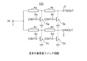
図10は、従来の高周波スイッチ回路の回路構成を示す図である。高周波スイッチ回路100は、入力端子(IN)1から2つの経路に分岐し、送信側出力端子(TXOUT)2及び受信側出力端子(RXOUT)3に接続される。送信側経路(入力端子1−送信側出力端子2間の経路)においては、4分の1波長(λ/4)の線路長を有する伝送線路4a、4bが入力端子1と送信側出力端子2の間に縦続接続(直列に接続)され、それらの接点にFET5a、5bが並列接続されている。同様に、受信側経路(入力端子1−受信側出力端子3間の経路)においては、4分の1波長の線路長を有する伝送線路4c、4dが入力端子1と受信側出力端子3の間に縦続接続され、それらの接点にFET5c、5dが並列接続されている。
FIG. 10 is a diagram showing a circuit configuration of a conventional high-frequency switch circuit. The high-
FET5a〜5dは、スイッチとして機能し、高周波スイッチ回路100において経路の切替制御を行うために設けられている。FET5a、5bのドレイン端子は、伝送線路4aと4bの相互接続点、伝送線路4bと送信側出力端子2の相互接続点にそれぞれ接続されている。FET5c、5dのドレイン端子は、伝送線路4cと4dの相互接続点、伝送線路4dと受信側出力端子3の相互接続点にそれぞれ接続されている。また、FET5a〜5dのソース端子はそれぞれ接地され、FET5a〜5dのゲート端子はそれぞれ制御端子(CONT)6a〜6dに接続されている。制御端子6a〜6dから制御電圧をFET5a〜5dのゲート端子に印加することで、FET5a〜5dのインピーダンスをそれぞれ変化させ、高周波スイッチ回路100での経路切替を行う。
The
図11は、図10に示した従来の高周波スイッチ回路100の送信切替時の等価回路を示す図である。送信切替時には、制御端子6a〜6dを介して供給される制御電圧によりFET5a、5bがオフされ、FET5c、5dがオンされる(使用されているFETのオフ容量値をCoffとし、オン抵抗値をRONとする。)。
FIG. 11 is a diagram showing an equivalent circuit at the time of transmission switching of the conventional high-
このとき、図11に示したように、受信側経路においては、オン抵抗RONは十分小さい値になるように選ばれるため、ノードN21からノードN22を見たときのインピーダンスは大きくなり、高周波信号は受信側出力端子3に到達することができない。一方、送信側経路においては、オフ容量Coffは十分小さい値になるように選ばれるため、ノードN11からグランドを見たときのインピーダンスは大きくなり、高周波信号は損失なく送信側出力端子2に到達する。
At this time, as shown in FIG. 11, the on-resistance R ON is selected to be a sufficiently small value in the reception side path, so that the impedance when the node N22 is viewed from the node N21 becomes large, and the high-frequency signal Cannot reach the
図12は、従来技術において一般的に使用されるFETの模式的な断面図を示す図である。図12において、120は基板(例えばInP)、121はバッファ層、122は(高純度)チャネル層、123はキャリア供給層である。また、Sはソース電極、Gはゲート電極、Dはドレイン電極である。ここで、マイクロ波以上の高い周波数でトランジスタを使用するためには、オン抵抗RONを小さくするため、ソース電極Sとゲート電極Gとの間の距離Lsg、及びゲート電極Gとドレイン電極Dとの間の距離Lgdを十分短くする必要がある。 FIG. 12 is a schematic cross-sectional view of an FET generally used in the prior art. In FIG. 12, 120 is a substrate (for example, InP), 121 is a buffer layer, 122 is a (high purity) channel layer, and 123 is a carrier supply layer. S is a source electrode, G is a gate electrode, and D is a drain electrode. Here, in order to use the transistor at a frequency higher than the microwave, the distance L sg between the source electrode S and the gate electrode G and the gate electrode G and the drain electrode D are reduced in order to reduce the on-resistance R ON. It is necessary to sufficiently shorten the distance L gd between the two.
しかし、距離Lsg及びLgdをそれぞれ短くすると、トランジスタのブレークダウン電圧が小さくなり、以下のような問題が生じる。図13は、図10に示した高周波スイッチ回路100において、FET5aがオフ状態であるときに大電力の高周波信号が送信側出力端子2から供給されてきた場合のFET5aのゲート−ドレイン(GD)間電圧Vgdの変動と、それに伴うFET5aよりノードN11に流れる電流IN11との関係を示す図である。
However, if the distances L sg and L gd are shortened, the breakdown voltage of the transistor is reduced, causing the following problems. FIG. 13 shows the relationship between the gate and drain (GD) of the
距離Lsg及びLgdがそれぞれ短いとFETのブレークダウン電圧Vbrが小さいために、制御端子を介してゲート端子に供給する制御電圧VCONTを大きくすることができない。そのため、図13に示したように、大電力の高周波信号入力時には、FET5aのGD間電圧Vgdが正側にふれてしまい(図13に示す破線部130)、FET5aのドレイン−ソース(DS)間に電流が流れてしまう。
When the distances L sg and L gd are short, the breakdown voltage Vbr of the FET is small, so that the control voltage V CONT supplied to the gate terminal through the control terminal cannot be increased. Therefore, as shown in FIG. 13, when a high-power high-frequency signal is input, the voltage Vgd between the GDs of the
すなわち、図10に示したような高周波スイッチ回路100において、FETはオフ状態にしているときには直流的には電流が流れないことが望ましいが、大電力の高周波信号入力時には直流的な電流が流れてしまう。これは高周波スイッチ回路の歪み特性を大幅に悪化させるため、従来の高周波スイッチ回路においては良好な歪み特性を得ることができなかった。
That is, in the high-
本発明は、耐高電圧特性及び良好な歪み特性を有するスイッチ回路を提供することを目的とする。 An object of the present invention is to provide a switch circuit having high voltage resistance characteristics and good distortion characteristics.
本発明のスイッチ回路は、入力端子に一端が接続された不平衡線路の他端と第1の出力端子との間に接続された第1の平衡線路と、上記不平衡線路の他端と第2の出力端子との間に接続された第2の平衡線路とを備える。各平衡線路は、複数の4分の1波長伝送線路が縦続接続され、かつインピーダンスを制御可能な複数の被制御回路が伝送線路の相互接続点毎に平衡線路を構成する1組の伝送線路対間に接続される。
上記構成によれば、各平衡線路では、従来のように不平衡線路を用いた場合と比較して、信号の電力が1対の伝送線路の双方に分配され、入力される電力が正味半分になる。
The switch circuit of the present invention includes a first balanced line connected between the other end of the unbalanced line whose one end is connected to the input terminal and the first output terminal, and the other end of the unbalanced line and the first And a second balanced line connected between the two output terminals. Each balanced line includes a pair of transmission line pairs in which a plurality of quarter-wave transmission lines are cascaded and a plurality of controlled circuits capable of controlling impedance constitute a balanced line for each interconnection point of the transmission lines. Connected between.
According to the above configuration, in each balanced line, the signal power is distributed to both the pair of transmission lines and the input power is halved compared to the case of using an unbalanced line as in the prior art. Become.
本発明によれば、各平衡線路においては従来のように不平衡線路を用いた場合と比較して入力される電力が半分になるので、大電力の高周波信号が入力されても、スイッチ回路のFETがオフ状態であるときに直流的に電流が流れることを防止し、良好な歪み特性を得ることができる。 According to the present invention, the power input to each balanced line is halved compared to the conventional case using an unbalanced line. It is possible to prevent a current from flowing in a direct current when the FET is in an off state, and to obtain good distortion characteristics.
以下、本発明の実施形態を図面に基づいて説明する。
図1は、本発明の実施形態によるスイッチ回路の一例である高周波スイッチ回路の回路構成例を示す図である。本実施形態における高周波スイッチ回路10は、高周波領域で動作可能なスイッチ回路であり、図1に示すように、平衡伝送線路4a、4a’、4b、4b’、4c、4c’、4d、及び4d’と電界効果トランジスタ(FET)5a、5b、5c、及び5dとを有する。
Hereinafter, embodiments of the present invention will be described with reference to the drawings.
FIG. 1 is a diagram illustrating a circuit configuration example of a high-frequency switch circuit which is an example of a switch circuit according to an embodiment of the present invention. The high-
また、高周波スイッチ回路10は、入力端子(IN)1と、送信側出力端子(TXOUT、/TXOUT)2a、2b及び受信側出力端子(RXOUT、/RXOUT)3a、3bとを有する。入力端子1は、不平衡線路を経て、分岐された2つの経路(2つの平衡線路)を介して送信側出力端子2a、2b及び受信側出力端子3a、3bに接続される。一方の経路では、入力端子1は、不平衡線路及び平衡伝送線路4a、4a’、4b、4b’を介して送信側出力端子2a、2bに接続される。また、他方の経路では、入力端子1は、不平衡線路及び平衡伝送線路4c、4c’、4d、4d’を介して受信側出力端子3a、3bに接続される。
The high-
具体的には、一方の経路においては、4分の1波長(λ/4)の電気長(線路長)を有する伝送線路4a、4bが入力端子1(より詳細には入力端子1に一端が接続された不平衡線路)と送信側出力端子2aの間に縦続接続(直列に接続)され、(λ/4)の電気長を有する伝送線路4a’、4b’が送信側出力端子2bに対して縦続接続される。伝送線路4a、4a’、4b、4b’により構成される平衡伝送線路の線路対間にFET5a、5bが接続される。詳細には、FET5aのドレイン電極は平衡線路対の一方の線路を構成する伝送線路4aと4bの相互接続点に接続され、FET5bのドレイン電極は平衡線路の一方の伝送線路4bと送信側出力端子2aとの相互接続点に接続される。FET5aのソース電極は平衡線路対の他方の線路を構成する伝送線路4a’と4b’の相互接続点に接続され、FET5bのソース電極は平衡線路の他方の伝送線路4b’と送信側出力端子2bとの相互接続点に接続される。また、FET5a、5bのゲート電極は、制御電圧が供給される制御端子(CONT)6a、6bにそれぞれ接続される。
Specifically, in one path,
また、他方の経路においては、(λ/4)の電気長を有する伝送線路4c、4dが受信側出力端子3aに対して縦続接続され、(λ/4)の電気長を有する伝送線路4c’、4d’が入力端子1(より詳細には入力端子1に一端が接続された不平衡線路)と受信側出力端子3bの間に縦続接続される。伝送線路4c、4c’、4d、4d’により構成される平衡伝送線路の線路対間にFET5c、5dが接続される。FET5c、5dのドレイン電極は、平衡線路対の一方の線路に係る伝送線路4cと4dの相互接続点、伝送線路4dと受信側出力端子3aとの相互接続点にそれぞれ接続される。FET5c、5dのソース電極は、平衡線路対の他方の線路に係る伝送線路4c’と4d’の相互接続点、伝送線路4d’と受信側出力端子3bとの相互接続点に接続される。また、FET5c、5dのゲート電極は、制御電圧が供給される制御端子(CONT)6c、6dにそれぞれ接続される。
In the other path,
FET5a〜5dは、高周波スイッチ回路10において経路の切替制御を行うためスイッチとして機能する。図1に示した高周波スイッチ回路10は、制御端子6a〜6dよりFET5a〜5dのゲート電極に印加する制御電圧を制御して、FET5a〜5dにおけるゲート電圧を基にFET5a〜5dのインピーダンスを切り替えることで、高周波スイッチ回路10での経路切替を選択することができる。
The
例えば、図1に示した高周波スイッチ回路10において送信側経路に切り替えた場合、高周波スイッチ回路10の等価回路は図2に示される。
すなわち、FET5a、5bは制御端子6a、6bを介して供給される制御電圧によりともにオフされ、容量素子(オフ容量値Coff)とみなすことができる。この場合、容量値Coffが十分小さければ、高周波領域においてもノードN11からノードN11’を見たときのインピーダンスは十分大きくなり送信側経路を通過する高周波信号は損失なく入力端子1まで到達する。
For example, when the high
That is, the
また、FET5c、5dは制御端子6c、6dを介して供給される制御電圧によりともにオンされ、抵抗素子(オン抵抗値RON)とみなすことができる。この場合、抵抗値RONが十分小さければ、高周波領域においてもノードN21からノードN21’を見たときのインピーダンスは十分小さくなる。ここで、伝送線路4c、4c’の電気長はそれぞれ4分の1波長である。したがって、入力端子1に入力された信号は受信側経路に入る前に反射される。以上のようにして、図1に示した高周波スイッチ回路10において送信側経路に切り替えた場合には、不平衡・平衡の伝送モードの切替が行われるとともに、すべての信号は送信側回路に送られ伝送される。
なお、同様に図1に示した高周波スイッチ回路10において送信側経路に切り替えた場合には、FET5a、5bはオンされて抵抗素子とみなし、FET5c、5dはオフされて容量素子とみなすことができるので、不平衡・平衡での伝送モードの切替が行われるとともに、すべての信号は受信側回路により伝送される。
The
Similarly, when the high-
ここで、図1に示した高周波スイッチ回路10において送信側経路に切り替え、送信側経路を大電力の高周波信号が通過する場合について考える。図1に示した高周波スイッチ回路10は、図10に示したような従来の高周波スイッチ回路とは異なり、平衡線路を構成する1対の伝送線路の両側に電力が分配される。したがって、ノードN11における高周波信号による電圧振幅の大きさは、従来と比較して正味半分の大きさになる。
Here, consider a case where the high-
図3は、図1に示した高周波スイッチ回路10において、FET5aがオフ状態であるときに大電力の高周波信号が送信側出力端子2a、2bから供給されてきた場合のFET5aのゲート−ドレイン(GD)間電圧Vgdの変動と、それに伴うFET5aよりノードN11に流れる電流IN11との関係を示す図である。図3において横軸は電流IN11であり、縦軸はFET5aのGD間電圧Vgdである。
FIG. 3 shows the gate-drain (GD) of the
上述したように、本実施形態における高周波スイッチ回路10では、従来の高周波スイッチ回路とは異なり、ノードN11における電圧振幅の大きさは半分の大きさとなる。そのため、大電力の高周波信号が入力されても、FET5aのGD間電圧Vgdが正側にふれてしまうことを抑制することができ、オフ状態にしているときに直流的な電流が流れることを防止することができる。したがって、本実施形態の高周波スイッチ回路10によれば、高周波スイッチ回路の歪み特性が悪化することを防止し、良好な歪み特性を得ることができる。
As described above, in the high-
本実施形態の高周波スイッチ回路10によれば、高い周波数帯で使用するために高周波スイッチ回路に使用するFETのソース電極Sとゲート電極Gとの間の距離Lsg、及びゲート電極Gとドレイン電極Dとの間の距離Lgdをたとえ短くしても、FETのGD間電圧Vgdが正側にふれてしまうことを抑制して良好な歪み特性を得ることができる。
According to the high
次に、図1に示した本実施形態における高周波スイッチ回路10の各特性について説明する。
まず、ミリ波帯における通過特性(損失特性)とアイソレーション特性について、図4を参照して説明する。図4においては、本実施形態における高周波スイッチ回路10の特性と、比較参照するために図10に示した従来の高周波スイッチ回路100の特性とを示している。
Next, each characteristic of the high
First, passing characteristics (loss characteristics) and isolation characteristics in the millimeter wave band will be described with reference to FIG. 4 shows the characteristics of the high-
図4において、横軸は信号の周波数であり、縦軸は損失及びアイソレーションである。また、S11及びS21は、本実施形態における高周波スイッチ回路10の損失特性及びアイソレーション特性をそれぞれ示しており、S12及びS22は、従来の高周波スイッチ回路100の損失特性及びアイソレーション特性をそれぞれ示している。
In FIG. 4, the horizontal axis represents the signal frequency, and the vertical axis represents the loss and isolation. S11 and S21 show the loss characteristic and isolation characteristic of the high-
図4に示されるように、本実施形態における高周波スイッチ回路10の通過特性(損失特性)及びアイソレーション特性は、従来技術とほぼ同等の性能を有していることが分かる。
As shown in FIG. 4, it can be seen that the pass characteristic (loss characteristic) and the isolation characteristic of the high-
次に、大電力の信号を入力した場合の特性について、図5(A)を参照して説明する。図5(A)においても、本実施形態における高周波スイッチ回路10の特性と、比較参照するために従来の高周波スイッチ回路100の特性とをそれぞれ示している。
Next, characteristics when a high-power signal is input will be described with reference to FIG. FIG. 5A also shows the characteristics of the high-
図5(A)において、横軸は信号の入力パワー(入力電力)であり、縦軸は信号の出力パワー(出力電力)及び損失量(出力パワーと入力パワーとの差分)である。また、図5(A)において、OP11及びL11は本実施形態における高周波スイッチ回路10の特性を示しており、OP11は入力パワーに応じた出力パワーを示し、L11は入力パワーに応じた損失量を示している。同様にOP12及びL12は従来の高周波スイッチ回路100の特性を示しており、OP12は入力パワーに応じた出力パワーを示し、L12は入力パワーに応じた損失量を示している。
In FIG. 5A, the horizontal axis represents signal input power (input power), and the vertical axis represents signal output power (output power) and loss (difference between output power and input power). In FIG. 5A, OP11 and L11 indicate the characteristics of the high-
図5(A)から分かるように、入力される電力が小さいときには、本実施形態と従来技術との間で通過特性(損失特性)について違いは見つけられないが、電力が大きくなっていくにつれてその違いは顕著になる。大電力の信号が入力された時の利得コンプレッションは、本実施形態の高周波スイッチ回路よりも従来技術の方が大きいことが確認できる。歪み特性を表す指標の1つであるPi1dB(低電力の信号入力時の損失よりも1dBだけ損失が増える入力パワー)でいえば、本実施形態では従来技術と比較して3dB改善している。 As can be seen from FIG. 5A, when the input power is small, no difference is found in the pass characteristic (loss characteristic) between the present embodiment and the prior art, but as the power increases The difference becomes noticeable. It can be confirmed that the gain compression when a high-power signal is input is larger in the conventional technique than in the high-frequency switch circuit of the present embodiment. Speaking of Pi1 dB (input power in which the loss is increased by 1 dB over the loss at the time of low power signal input), which is one of the indexes representing the distortion characteristics, the present embodiment is improved by 3 dB as compared with the prior art.
次に、大電力を入力した場合の高調波特性について、図5(B)を参照して説明する。図5(B)においても、本実施形態における高周波スイッチ回路10の高調波特性と、比較参照するために従来の高周波スイッチ回路100の高調波特性とをそれぞれ示している。
Next, harmonic characteristics when large power is input will be described with reference to FIG. FIG. 5B also shows the harmonic characteristics of the high-
図5(B)において、横軸は信号の入力パワー(入力電力)であり、縦軸は信号の出力パワー(出力電力)である。また、図5(B)において、OP11、OP21、OP31は本実施形態における高周波スイッチ回路10の高調波特性(それぞれ基本波、2倍高調波、3倍高調波)を示しており、OP12、OP22、OP32は従来の高周波スイッチ回路100の高調波特性(基本波、2倍高調波、3倍高調波)を示している。なお、基本波の周波数は、60GHzである。
図5(B)から明らかなように、本実施形態における高周波スイッチ回路10は、2倍高調波、3倍高調波ともに従来と比較して小さくなっていることが確認できる。
In FIG. 5B, the horizontal axis represents signal input power (input power), and the vertical axis represents signal output power (output power). In FIG. 5B, OP11, OP21, and OP31 indicate harmonic characteristics (respectively fundamental wave, second harmonic wave, and third harmonic wave) of the high-
As is apparent from FIG. 5B, it can be confirmed that the high-
図5(A)及び(B)に示したように、本実施形態における高周波スイッチ回路10は、大電力の信号入力時の歪み特性が従来技術に比べて改善していることが分かる。
As shown in FIGS. 5A and 5B, the high-
次に、本実施形態における高周波スイッチ回路の他の構成例について説明する。
図6は、本実施形態における高周波スイッチ回路の他の回路構成例を示す図である。この図6において、図1に示した構成要素と同一の機能を有する構成要素には同一の符号を付し、重複する説明は省略する。
Next, another configuration example of the high-frequency switch circuit in the present embodiment will be described.
FIG. 6 is a diagram illustrating another circuit configuration example of the high-frequency switch circuit according to the present embodiment. In FIG. 6, components having the same functions as those shown in FIG. 1 are given the same reference numerals, and redundant descriptions are omitted.
図6に示す高周波スイッチ回路20は、FET5a、5b、5c、5dに換えてダイオード11a、11b、11c、11dを用いた点が図1に示した高周波スイッチ回路10とは異なる。
The high-
具体的には、高周波スイッチ回路20において、ダイオード11aのカソードは平衡線路対の一方の線路に係る伝送線路4aと4bの相互接続点に接続され、アノードは容量12aの一方の電極に接続される。容量12aの他方の電極は、平衡線路対の他方の線路に係る伝送線路4a’と4b’の相互接続点に接続される。また、ダイオード11aのアノードと容量12aの一方の電極との相互接続点が、抵抗13aを介して、制御電圧が供給される制御端子(CONT)14aに接続される。
Specifically, in the high-
なお、高周波スイッチ回路20において、高周波スイッチ回路10のFET5b、5c、5dに対応するダイオード11b、11c、11dが用いられる部分も、それぞれ1組のダイオード、容量、及び抵抗がダイオード11aに係る部分と同様に接続されて構成されるので詳細な説明は省略する。また、動作原理等については、図1に示した高周波スイッチ回路10と同様であるので説明は省略する。
In the high-
図7は、本実施形態における高周波スイッチ回路のその他の構成例を示す図である。この図7において、図1に示した構成要素と同一の機能を有する構成要素には同一の符号を付し、重複する説明は省略する。 FIG. 7 is a diagram illustrating another configuration example of the high-frequency switch circuit according to the present embodiment. In FIG. 7, components having the same functions as those shown in FIG. 1 are given the same reference numerals, and redundant description is omitted.
図7に示す高周波スイッチ回路30は、出力側端子をBALUN(バルン)回路に接続していることが図1に示した高周波スイッチ回路10とは異なる。図7に示す高周波スイッチ回路30は、平衡・不平衡変換を行う変換回路であるバルン回路を接続したことで出力側において不平衡の信号を得ることができる。
The high
高周波スイッチ回路30の送信側経路においては、伝送線路4bとFET5bのドレインとの相互接続点と、伝送線路4b’とFET5bのソースとの相互接続点との間に(λ/4)の電気長を有する伝送線路21a、21bが直列に接続(縦続接続)される。また、伝送線路4b’と21bの相互接続点が送信側出力端子(TXOUT)2に接続される。ここで、伝送線路21a、21bの電気長は足し合わせると半波長になるため、平衡伝送線路4a、4a’、4b、4b’を伝送されてきた信号(平衡信号)は不平衡信号に変換される。
In the transmission side path of the high-
一方、受信側経路においては、伝送線路4d’とFET5dのソースとの相互接続点と、伝送線路4dとFET5dのドレインとの相互接続点との間に(λ/4)の電気長を有する伝送線路22a、22bが直列に接続される。また、伝送線路4dと22bの相互接続点が受信側出力端子(RXOUT)3に接続される。伝送線路22a、22bの電気長は足し合わせると半波長になるため、平衡伝送線路4c、4c’、4d、4d’を伝送されてきた信号(平衡信号)は不平衡信号に変換される。
On the other hand, in the reception side path, transmission having an electrical length of (λ / 4) between the interconnection point between the
なお、高周波スイッチ回路30の動作原理等については、図1に示した高周波スイッチ回路10と同様であるのでここでは説明は省略する。
The operating principle of the high
図1、図7に示した本実施形態における高周波スイッチ回路10、30に用いるFET5a〜5dとして適用可能なトランジスタの一覧を図8に示している。図8において、例示したトランジスタに付してある記号は、丸、三角、バツの順に適性が低くなるものとする。図8に示すように本実施形態におけるスイッチ回路においては、トランジスタ素子として、HEMT(high electron mobility transistor:高電子移動度トランジスタ)やHBT(hetero-junction bipolar transistor:ヘテロ接合バイポーラトランジスタ)など適用可能である。
FIG. 8 shows a list of transistors applicable as the
図9は、上述した本実施形態における高周波スイッチ回路を用いて構成したRF(高周波信号)トランシーバー装置の構成例を示す図である。
図9において、81は高出力電圧制御発振器(VCO)、82はミキサ(アップコンバータ)、83はドライバ、84はバンドパスフィルタ(BPF)、85は可変アッテネータ、86は高出力増幅器(AMP)、87は送受信用アンテナである。また、88は低雑音増幅器(LNA)、89はバンドパスフィルタ(BPF)、90は可変アッテネータ、91はミキサ(ダウンコンバータ)、SW1及びSW2はSPDTスイッチである。
FIG. 9 is a diagram illustrating a configuration example of an RF (high frequency signal) transceiver device configured using the high frequency switch circuit according to the present embodiment described above.
In FIG. 9, 81 is a high output voltage controlled oscillator (VCO), 82 is a mixer (upconverter), 83 is a driver, 84 is a band pass filter (BPF), 85 is a variable attenuator, 86 is a high output amplifier (AMP),
送信信号入力端子SSより入力される送信IF信号(中間周波信号)は、スイッチSW1(SPDT1)を介して供給される高出力VCO81の発振信号を基に、アップコンバータ82にて送信RF信号(高周波信号)に変換される。アップコンバータ82から出力された送信RF信号は、ドライバ83を介してBPF84にてフィルタ処理が施され不要な周波数成分がカットされる。
The transmission IF signal (intermediate frequency signal) input from the transmission signal input terminal SS is transmitted by the up-
そして、BPF84から出力された送信RF信号は、可変減衰器85にて所定の減衰量で減衰されて出力レベル調整され、さらに高出力増幅器86にて増幅される。高出力増幅器86で増幅された送信RF信号は、スイッチSW2(SPDT2)を介して送受信用アンテナ87に供給され、送受信用アンテナ87より送信される。
The transmission RF signal output from the
ここで、送信信号には大きな電力と小さな歪みとが要求されるため、本実施形態における高周波スイッチ回路は、送受信用アンテナ87の直近に配置されるスイッチSW2(SPDT2)に適用される。なお、さらに本実施形態における高周波スイッチ回路をスイッチSW1(SPDT1)に適用しても良い。
Here, since a high power and a small distortion are required for the transmission signal, the high-frequency switch circuit in this embodiment is applied to the switch SW2 (SPDT2) disposed in the immediate vicinity of the transmission /
また、送受信用アンテナ87で受信された受信RF信号は、スイッチSW2(SPDT2)を介して低雑音増幅器88に供給され、低雑音増幅器88にて増幅される。低雑音増幅器88で増幅された受信RF信号は、BPF84にてフィルタ処理が施された後、ダウンコンバータ91に供給される。
ダウンコンバータ91に供給された受信RF信号は、高出力VCO81の発振信号に基づくローカル発振信号を基に、ダウンコンバータ91にて受信IF信号に変換され、受信信号出力端子RSより出力される。
The received RF signal received by the transmission /
The reception RF signal supplied to the
なお、上述した本実施形態におけるスイッチ回路は、それを構成するFET(トランジスタ)と(λ/4)の伝送線路とを同一の半導体基板上にモノリシックに集積したモノリシック集積回路として構成可能である。また、スイッチ回路におけるFETなどの能動素子を半導体基板上に集積し、伝送線路などの受動素子を誘電体基板上に集積し、能動素子を集積した半導体基板と受動素子を集積した誘電体基板とを実装したハイブリッド集積回路としても構成可能である。 Note that the switch circuit according to the present embodiment described above can be configured as a monolithic integrated circuit in which FETs (transistors) and (λ / 4) transmission lines constituting the switch circuit are monolithically integrated on the same semiconductor substrate. Also, active elements such as FETs in a switch circuit are integrated on a semiconductor substrate, passive elements such as transmission lines are integrated on a dielectric substrate, a semiconductor substrate on which active elements are integrated, and a dielectric substrate on which passive elements are integrated It can also be configured as a hybrid integrated circuit mounted with.
なお、上記実施形態は、何れも本発明を実施するにあたっての具体化のほんの一例を示したものに過ぎず、これらによって本発明の技術的範囲が限定的に解釈されてはならないものである。すなわち、本発明はその技術思想、またはその主要な特徴から逸脱することなく、様々な形で実施することができる。
本発明の諸態様を付記として以下に示す。
The above-described embodiments are merely examples of implementation in carrying out the present invention, and the technical scope of the present invention should not be construed as being limited thereto. That is, the present invention can be implemented in various forms without departing from the technical idea or the main features thereof.
Various aspects of the present invention will be described below as supplementary notes.
(付記1)一端が入力端子に接続された不平衡線路と、
上記不平衡線路の他端と第1の出力端子との間に接続された第1の平衡線路と、
上記不平衡線路の上記他端と第2の出力端子との間に接続された第2の平衡線路とを備え、
上記第1及び第2の平衡線路のそれぞれは、
縦続接続された複数の4分の1波長伝送線路と、
上記縦続接続された4分の1波長伝送線路の相互接続点毎に上記平衡線路を構成する1組の伝送線路対間に接続され、外部よりインピーダンスを制御可能な複数の被制御回路とを有することを特徴とするスイッチ回路。
(付記2)上記被制御回路は、制御電極に供給される制御電圧によりインピーダンス制御されるトランジスタ素子であることを特徴とする付記1記載のスイッチ回路。
(付記3)上記被制御回路は、ゲート電極に制御電圧が供給され、上記1組の伝送線路対の一方の伝送線路にドレイン電極が接続されるとともに他方の伝送線路にソース電極が接続された電界効果トランジスタであることを特徴とする付記1記載のスイッチ回路。
(付記4)上記トランジスタ素子は、HEMT(high electron mobility transistor)であることを特徴とする付記2記載のスイッチ回路。
(付記5)上記トランジスタ素子は、HBT(hetero-junction bipolar transistor)であることを特徴とする付記2記載のスイッチ回路。
(付記6)上記被制御回路は、上記1組の伝送線路対間に接続された2端子のダイオードを有することを特徴とする付記1記載のスイッチ回路。
(付記7)上記被制御回路は、2端子のダイオードと容量とを有し、
上記ダイオードは、上記1組の伝送線路対の一方の伝送線路にカソードが接続され、他方の伝送線路にアノードが上記容量を介して接続されるとともに、上記アノードに制御電圧が供給されることを特徴とする付記1記載のスイッチ回路。
(付記8)上記第1の平衡線路と上記第1の出力端子との間、及び上記第2の平衡線路と上記第2の出力端子との間の少なくとも一方に、平衡・不平衡変換を行う変換回路をさらに備えたことを特徴とする付記1記載のスイッチ回路。
(付記9)中間周波数信号を高周波数信号に変換して増幅しアンテナに対して出力する送信信号処理回路と、
上記アンテナで受信した高周波信号が供給され、当該高周波信号を増幅して中間周波数信号に変換する受信信号処理回路と、
上記送信信号処理回路又は上記受信信号処理回路を選択的に上記アンテナに対して信号を伝送可能なように接続するスイッチ回路とを備え、
上記スイッチ回路は、一端が上記アンテナに接続された不平衡線路と、
上記不平衡線路の他端と上記送信信号処理回路との間に接続された第1の平衡線路と、
上記不平衡線路の上記他端と上記受信信号処理回路との間に接続された第2の平衡線路とを備え、
上記第1及び第2の平衡線路のそれぞれは、
縦続接続された複数の4分の1波長伝送線路と、
上記縦続接続された4分の1波長伝送線路の相互接続点毎に上記平衡線路を構成する1組の伝送線路対間に接続され、外部よりインピーダンスを制御可能な複数の被制御回路とを有することを特徴とする集積回路。
(付記10)付記2記載のスイッチ回路の上記トランジスタ素子を集積した半導体チップと、当該スイッチ回路の上記伝送線路を集積した誘電体基板とを備えることを特徴とする集積回路。
(付記11)付記2記載のスイッチ回路の上記トランジスタ素子と上記伝送線路を同一の半導体基板上に集積したことを特徴とする集積回路。
(Appendix 1) An unbalanced line with one end connected to the input terminal;
A first balanced line connected between the other end of the unbalanced line and a first output terminal;
A second balanced line connected between the other end of the unbalanced line and a second output terminal;
Each of the first and second balanced lines is
A plurality of quarter-wave transmission lines connected in cascade;
A plurality of controlled circuits that are connected between a pair of transmission lines constituting the balanced line at each interconnection point of the cascaded quarter-wavelength transmission lines and that can control impedance from the outside; A switch circuit characterized by that.
(Supplementary note 2) The switch circuit according to supplementary note 1, wherein the controlled circuit is a transistor element whose impedance is controlled by a control voltage supplied to a control electrode.
(Supplementary Note 3) In the controlled circuit, a control voltage is supplied to a gate electrode, a drain electrode is connected to one transmission line of the pair of transmission lines, and a source electrode is connected to the other transmission line. The switch circuit according to appendix 1, which is a field effect transistor.
(Supplementary note 4) The switch circuit according to Supplementary note 2, wherein the transistor element is a HEMT (high electron mobility transistor).
(Supplementary note 5) The switch circuit according to supplementary note 2, wherein the transistor element is an HBT (hetero-junction bipolar transistor).
(Supplementary note 6) The switch circuit according to supplementary note 1, wherein the controlled circuit includes a two-terminal diode connected between the pair of transmission lines.
(Appendix 7) The controlled circuit has a two-terminal diode and a capacitor,
The diode has a cathode connected to one transmission line of the pair of transmission lines, an anode connected to the other transmission line via the capacitor, and a control voltage supplied to the anode. The switch circuit according to Supplementary Note 1, wherein
(Supplementary note 8) Balance / unbalance conversion is performed between at least one of the first balanced line and the first output terminal and between the second balanced line and the second output terminal. The switch circuit according to appendix 1, further comprising a conversion circuit.
(Supplementary Note 9) A transmission signal processing circuit that converts an intermediate frequency signal into a high frequency signal, amplifies the signal, and outputs the signal to an antenna;
A high-frequency signal received by the antenna, a reception signal processing circuit for amplifying the high-frequency signal and converting it to an intermediate frequency signal;
A switch circuit for selectively connecting the transmission signal processing circuit or the reception signal processing circuit to the antenna so as to transmit the signal,
The switch circuit has an unbalanced line with one end connected to the antenna;
A first balanced line connected between the other end of the unbalanced line and the transmission signal processing circuit;
A second balanced line connected between the other end of the unbalanced line and the received signal processing circuit;
Each of the first and second balanced lines is
A plurality of quarter-wave transmission lines connected in cascade;
A plurality of controlled circuits that are connected between a pair of transmission lines constituting the balanced line at each interconnection point of the cascaded quarter-wavelength transmission lines and that can control impedance from the outside; An integrated circuit characterized by that.
(Additional remark 10) The integrated circuit characterized by including the semiconductor chip which integrated the said transistor element of the switch circuit of Additional remark 2, and the dielectric substrate which integrated the said transmission line of the said switch circuit.
(Additional remark 11) The integrated circuit which integrated the said transistor element and the said transmission line of the switch circuit of Additional remark 2 on the same semiconductor substrate.
10、20、30 高周波スイッチ回路
1 入力端子
2a、2b 送信側出力端子
3a、3b 受信側出力端子
4a、4a’、4b、4b’、4c、4c’、4d、4d’ 伝送線路
5a、5b、5c、5d トランジスタ(FET)
6a、6b、6c、6d 制御端子
10, 20, 30 High-frequency switch circuit 1
6a, 6b, 6c, 6d Control terminal
Claims (10)
上記不平衡線路の他端と第1の出力端子との間に接続された第1の平衡線路と、
上記不平衡線路の上記他端と第2の出力端子との間に接続された第2の平衡線路とを備え、
上記第1及び第2の平衡線路のそれぞれは、
縦続接続された複数の4分の1波長伝送線路と、
上記縦続接続された4分の1波長伝送線路の相互接続点毎に上記平衡線路を構成する1組の伝送線路対間に接続され、外部よりインピーダンスを制御可能な複数の被制御回路とを有することを特徴とするスイッチ回路。 An unbalanced line with one end connected to the input terminal;
A first balanced line connected between the other end of the unbalanced line and a first output terminal;
A second balanced line connected between the other end of the unbalanced line and a second output terminal;
Each of the first and second balanced lines is
A plurality of quarter-wave transmission lines connected in cascade;
A plurality of controlled circuits that are connected between a pair of transmission lines constituting the balanced line at each interconnection point of the cascaded quarter-wavelength transmission lines and that can control impedance from the outside; A switch circuit characterized by that.
上記ダイオードは、上記1組の伝送線路対の一方の伝送線路にカソードが接続され、他方の伝送線路にアノードが上記容量を介して接続されるとともに、上記アノードに制御電圧が供給されることを特徴とする請求項1記載のスイッチ回路。 The controlled circuit has a two-terminal diode and a capacitor,
The diode has a cathode connected to one transmission line of the pair of transmission lines, an anode connected to the other transmission line via the capacitor, and a control voltage supplied to the anode. The switch circuit according to claim 1.
上記アンテナで受信した高周波信号が供給され、当該高周波信号を増幅して中間周波数信号に変換する受信信号処理回路と、
上記送信信号処理回路又は上記受信信号処理回路を選択的に上記アンテナに対して信号を伝送可能なように接続するスイッチ回路とを備え、
上記スイッチ回路は、一端が上記アンテナに接続された不平衡線路と、
上記不平衡線路の他端と上記送信信号処理回路との間に接続された第1の平衡線路と、
上記不平衡線路の上記他端と上記受信信号処理回路との間に接続された第2の平衡線路とを備え、
上記第1及び第2の平衡線路のそれぞれは、
縦続接続された複数の4分の1波長伝送線路と、
上記縦続接続された4分の1波長伝送線路の相互接続点毎に上記平衡線路を構成する1組の伝送線路対間に接続され、外部よりインピーダンスを制御可能な複数の被制御回路とを有することを特徴とする集積回路。 A transmission signal processing circuit that converts the intermediate frequency signal into a high frequency signal, amplifies it, and outputs it to the antenna;
A high-frequency signal received by the antenna, a reception signal processing circuit for amplifying the high-frequency signal and converting it to an intermediate frequency signal;
A switch circuit for selectively connecting the transmission signal processing circuit or the reception signal processing circuit to the antenna so as to transmit the signal,
The switch circuit has an unbalanced line with one end connected to the antenna;
A first balanced line connected between the other end of the unbalanced line and the transmission signal processing circuit;
A second balanced line connected between the other end of the unbalanced line and the received signal processing circuit;
Each of the first and second balanced lines is
A plurality of quarter-wave transmission lines connected in cascade;
A plurality of controlled circuits that are connected between a pair of transmission lines constituting the balanced line at each interconnection point of the cascaded quarter-wavelength transmission lines and that can control impedance from the outside; An integrated circuit characterized by that.
Priority Applications (4)
| Application Number | Priority Date | Filing Date | Title |
|---|---|---|---|
| JP2005287721A JP4106376B2 (en) | 2005-09-30 | 2005-09-30 | Switch circuit and integrated circuit |
| US11/362,506 US7511592B2 (en) | 2005-09-30 | 2006-02-27 | Switch circuit and integrated circuit |
| EP20060251081 EP1772964B1 (en) | 2005-09-30 | 2006-02-28 | High-frequency switch circuit |
| DE200660001341 DE602006001341D1 (en) | 2005-09-30 | 2006-02-28 | High-frequency circuit |
Applications Claiming Priority (1)
| Application Number | Priority Date | Filing Date | Title |
|---|---|---|---|
| JP2005287721A JP4106376B2 (en) | 2005-09-30 | 2005-09-30 | Switch circuit and integrated circuit |
Publications (2)
| Publication Number | Publication Date |
|---|---|
| JP2007104021A JP2007104021A (en) | 2007-04-19 |
| JP4106376B2 true JP4106376B2 (en) | 2008-06-25 |
Family
ID=37496694
Family Applications (1)
| Application Number | Title | Priority Date | Filing Date |
|---|---|---|---|
| JP2005287721A Expired - Fee Related JP4106376B2 (en) | 2005-09-30 | 2005-09-30 | Switch circuit and integrated circuit |
Country Status (4)
| Country | Link |
|---|---|
| US (1) | US7511592B2 (en) |
| EP (1) | EP1772964B1 (en) |
| JP (1) | JP4106376B2 (en) |
| DE (1) | DE602006001341D1 (en) |
Families Citing this family (10)
| Publication number | Priority date | Publication date | Assignee | Title |
|---|---|---|---|---|
| FR2931300B1 (en) * | 2008-05-16 | 2016-10-21 | Thales Sa | HYPERFREQUENCY SWITCH AND TRANSMITTING AND RECEIVING MODULE HAVING SUCH A SWITCH |
| US7893791B2 (en) * | 2008-10-22 | 2011-02-22 | The Boeing Company | Gallium nitride switch methodology |
| US8279019B2 (en) | 2010-05-10 | 2012-10-02 | Mediatek Singapore Pte. Ltd. | Millimeter-wave switches and attenuators |
| JP5735268B2 (en) * | 2010-12-20 | 2015-06-17 | サムソン エレクトロ−メカニックス カンパニーリミテッド. | High frequency semiconductor switch |
| KR101452063B1 (en) * | 2012-12-10 | 2014-10-16 | 삼성전기주식회사 | Front end module |
| CN103885011B (en) * | 2012-12-20 | 2017-04-05 | 西门子(深圳)磁共振有限公司 | A kind of adapter, coil and magnetic resonance imaging system |
| US20140179241A1 (en) * | 2012-12-20 | 2014-06-26 | Qualcomm Incorporated | Concurrent matching network using transmission lines for low loss |
| JP2015195449A (en) * | 2014-03-31 | 2015-11-05 | 三菱電機株式会社 | Multiband high frequency power amplifier |
| US10495685B2 (en) * | 2016-12-05 | 2019-12-03 | Electronics And Telecommunications Research Institute | Multi-source signal generator and operating method thereof |
| US10277205B1 (en) * | 2018-06-05 | 2019-04-30 | Samsung Electronics Co., Ltd. | SPDT switch with high linearity |
Family Cites Families (13)
| Publication number | Priority date | Publication date | Assignee | Title |
|---|---|---|---|---|
| JPH0435501A (en) * | 1990-05-31 | 1992-02-06 | Fujitsu Ltd | Switch circuit |
| JPH06232601A (en) | 1993-01-29 | 1994-08-19 | Mitsubishi Electric Corp | Microwave switch circuit |
| JP3198808B2 (en) * | 1994-06-30 | 2001-08-13 | 株式会社村田製作所 | High frequency switch |
| US5856713A (en) * | 1997-10-24 | 1999-01-05 | Raytheon Company | N-way MMIC switch |
| US5990580A (en) * | 1998-03-05 | 1999-11-23 | The Whitaker Corporation | Single pole double throw switch |
| JP2000077903A (en) | 1998-03-31 | 2000-03-14 | Toshiba Lighting & Technology Corp | Microwave spdt switch |
| JP2000286601A (en) | 1999-03-30 | 2000-10-13 | Matsushita Electric Ind Co Ltd | High-frequency switch device |
| JP2002164704A (en) | 2000-11-28 | 2002-06-07 | Matsushita Electric Ind Co Ltd | High frequency switch for dealing with balance signal, and spiral inductor and distributor |
| JP2003142931A (en) | 2001-11-07 | 2003-05-16 | Alps Electric Co Ltd | Monopole antenna |
| JP3729396B2 (en) | 2001-11-01 | 2005-12-21 | 日立金属株式会社 | High frequency components |
| JP2003143033A (en) | 2001-11-01 | 2003-05-16 | Hitachi Metals Ltd | High-frequency switching module |
| US6737933B2 (en) * | 2002-01-15 | 2004-05-18 | Nokia Corporation | Circuit topology for attenuator and switch circuits |
| US6798314B2 (en) * | 2002-12-26 | 2004-09-28 | Intel Corporation | Transmit/receive combiner using shunt admittance elements for isolation |
-
2005
- 2005-09-30 JP JP2005287721A patent/JP4106376B2/en not_active Expired - Fee Related
-
2006
- 2006-02-27 US US11/362,506 patent/US7511592B2/en active Active
- 2006-02-28 DE DE200660001341 patent/DE602006001341D1/en active Active
- 2006-02-28 EP EP20060251081 patent/EP1772964B1/en not_active Expired - Fee Related
Also Published As
| Publication number | Publication date |
|---|---|
| EP1772964B1 (en) | 2008-05-28 |
| US20070075589A1 (en) | 2007-04-05 |
| US7511592B2 (en) | 2009-03-31 |
| EP1772964A1 (en) | 2007-04-11 |
| DE602006001341D1 (en) | 2008-07-10 |
| JP2007104021A (en) | 2007-04-19 |
Similar Documents
| Publication | Publication Date | Title |
|---|---|---|
| JP4106376B2 (en) | Switch circuit and integrated circuit | |
| US8359067B2 (en) | Radio frequency device and mobile communication terminal using the same | |
| JP4202405B2 (en) | Variable attenuator and integrated circuit | |
| US7986927B2 (en) | Semiconductor integrated circuit device and high-frequency power amplifier module | |
| US20050079829A1 (en) | Antenna switch | |
| US7843280B2 (en) | Systems, methods, and apparatuses for high power complementary metal oxide semiconductor (CMOS) antenna switches using body switching and substrate junction diode controlling in multistacking structure | |
| US8115234B2 (en) | Semiconductor device | |
| US20050012547A1 (en) | High linearity doherty communication amplifier with phase control | |
| US10778211B2 (en) | Switching circuit and semiconductor module | |
| WO2000003490A1 (en) | Mobile telephone system | |
| KR100976627B1 (en) | Switching circuit for millimeter wave band applications | |
| JP2015005979A (en) | Transformer for monolithic microwave integrated circuits | |
| JP2004208221A (en) | High frequency band filtering apparatus and portable information terminal | |
| CN114567266A (en) | Low-power-consumption low-noise broadband amplifier | |
| KR20090122965A (en) | High frequency switch with low loss, low harmonics and improved linearity performance | |
| JP2006303775A (en) | Semiconductor circuit device and high frequency power amplification module | |
| Makhsuci et al. | A review of Doherty power amplifier and load modulated balanced amplifier for 5G technology | |
| JP2008147627A (en) | High isolation switching element for millimeter wave band control circuit | |
| US10666231B2 (en) | Balun arrangement | |
| US10756727B2 (en) | Switching circuit and high-frequency module | |
| JP4217106B2 (en) | Monolithic microwave integrated circuit | |
| US11563410B1 (en) | Systems and methods for multi-band power amplifiers | |
| Shiba et al. | F-band bidirectional amplifier using 75-nm InP HEMTs | |
| WO2023203858A1 (en) | High frequency circuit and communication device | |
| Torii et al. | High Power and High Efficiency GaN Power Amplifiers for Ku/Ka-Bands Wireless Communication Systems |
Legal Events
| Date | Code | Title | Description |
|---|---|---|---|
| A977 | Report on retrieval |
Free format text: JAPANESE INTERMEDIATE CODE: A971007 Effective date: 20070912 |
|
| A131 | Notification of reasons for refusal |
Free format text: JAPANESE INTERMEDIATE CODE: A131 Effective date: 20070918 |
|
| TRDD | Decision of grant or rejection written | ||
| A01 | Written decision to grant a patent or to grant a registration (utility model) |
Free format text: JAPANESE INTERMEDIATE CODE: A01 Effective date: 20080304 |
|
| A61 | First payment of annual fees (during grant procedure) |
Free format text: JAPANESE INTERMEDIATE CODE: A61 Effective date: 20080331 |
|
| R150 | Certificate of patent or registration of utility model |
Ref document number: 4106376 Country of ref document: JP Free format text: JAPANESE INTERMEDIATE CODE: R150 Free format text: JAPANESE INTERMEDIATE CODE: R150 |
|
| FPAY | Renewal fee payment (event date is renewal date of database) |
Free format text: PAYMENT UNTIL: 20110404 Year of fee payment: 3 |
|
| FPAY | Renewal fee payment (event date is renewal date of database) |
Free format text: PAYMENT UNTIL: 20110404 Year of fee payment: 3 |
|
| FPAY | Renewal fee payment (event date is renewal date of database) |
Free format text: PAYMENT UNTIL: 20120404 Year of fee payment: 4 |
|
| FPAY | Renewal fee payment (event date is renewal date of database) |
Free format text: PAYMENT UNTIL: 20130404 Year of fee payment: 5 |
|
| FPAY | Renewal fee payment (event date is renewal date of database) |
Free format text: PAYMENT UNTIL: 20140404 Year of fee payment: 6 |
|
| LAPS | Cancellation because of no payment of annual fees |