EP2383883A1 - Power amplifier - Google Patents
Power amplifier Download PDFInfo
- Publication number
- EP2383883A1 EP2383883A1 EP10250822A EP10250822A EP2383883A1 EP 2383883 A1 EP2383883 A1 EP 2383883A1 EP 10250822 A EP10250822 A EP 10250822A EP 10250822 A EP10250822 A EP 10250822A EP 2383883 A1 EP2383883 A1 EP 2383883A1
- Authority
- EP
- European Patent Office
- Prior art keywords
- amplifier
- output
- power amplifier
- stage
- transmission line
- Prior art date
- Legal status (The legal status is an assumption and is not a legal conclusion. Google has not performed a legal analysis and makes no representation as to the accuracy of the status listed.)
- Granted
Links
Images



Classifications
-
- H—ELECTRICITY
- H03—ELECTRONIC CIRCUITRY
- H03F—AMPLIFIERS
- H03F1/00—Details of amplifiers with only discharge tubes, only semiconductor devices or only unspecified devices as amplifying elements
- H03F1/02—Modifications of amplifiers to raise the efficiency, e.g. gliding Class A stages, use of an auxiliary oscillation
- H03F1/0205—Modifications of amplifiers to raise the efficiency, e.g. gliding Class A stages, use of an auxiliary oscillation in transistor amplifiers
- H03F1/0288—Modifications of amplifiers to raise the efficiency, e.g. gliding Class A stages, use of an auxiliary oscillation in transistor amplifiers using a main and one or several auxiliary peaking amplifiers whereby the load is connected to the main amplifier using an impedance inverter, e.g. Doherty amplifiers
-
- H—ELECTRICITY
- H03—ELECTRONIC CIRCUITRY
- H03F—AMPLIFIERS
- H03F1/00—Details of amplifiers with only discharge tubes, only semiconductor devices or only unspecified devices as amplifying elements
- H03F1/02—Modifications of amplifiers to raise the efficiency, e.g. gliding Class A stages, use of an auxiliary oscillation
- H03F1/0205—Modifications of amplifiers to raise the efficiency, e.g. gliding Class A stages, use of an auxiliary oscillation in transistor amplifiers
- H03F1/0294—Modifications of amplifiers to raise the efficiency, e.g. gliding Class A stages, use of an auxiliary oscillation in transistor amplifiers using vector summing of two or more constant amplitude phase-modulated signals
-
- H—ELECTRICITY
- H03—ELECTRONIC CIRCUITRY
- H03F—AMPLIFIERS
- H03F3/00—Amplifiers with only discharge tubes or only semiconductor devices as amplifying elements
- H03F3/60—Amplifiers in which coupling networks have distributed constants, e.g. with waveguide resonators
- H03F3/602—Combinations of several amplifiers
-
- H—ELECTRICITY
- H03—ELECTRONIC CIRCUITRY
- H03F—AMPLIFIERS
- H03F2200/00—Indexing scheme relating to amplifiers
- H03F2200/543—A transmission line being used as coupling element between two amplifying stages
Definitions
- a power amplifier comprising an input connected to first and second amplifier stages and an output stage configured to combine phase shifted amplified outputs from the first and second amplifier stages and to provide an amplified signal at an output of the power amplifier
- the impedances of the transmission lines 605a, 605b, 606 may be chosen such that the even and odd mode impedances of the coupled lines are 80 ⁇ (Z oe , or even mode impedance) and 44 ⁇ (Z oo , or odd mode impedance), and the impedance of the transmission line 75 ⁇ , and the electrical length of each of the lines selected to be one quarter wavelength.
- Other impedance values may alternatively be selected.
- the power amplifier 1200 comprises three amplifier stages including a first main amplifier stage 1201 and two further peak amplifier stages 1202a, 1202b.
Landscapes
- Engineering & Computer Science (AREA)
- Power Engineering (AREA)
- Amplifiers (AREA)
Abstract
Description
- The invention relates to improving the performance of load modulation power amplifiers through the use of coupled transmission line-based power combiners.
- Power amplifiers (PAs) that use load line modulation techniques to improve overall amplifier efficiency have been known for some time. Two well-known examples are in the form of a two-way Doherty amplifier, illustrated in
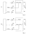
figure 1 , and a Chireix outphasing amplifier, illustrated infigure 2 . A two-way Doherty amplifier comprises twoamplifier stages peak amplifier 101 and a second being amain amplifier 102. Thepeak amplifier 101 amplifies a phase-shifted version of the input signal, while themain amplifier 102 amplifies an unshifted version. Acombiner stage 103 combines the output signals from theamplifier stages load 104. A Chireix outphasing amplifier operates according to a similar principle, with twoamplifier stages combiner stage 203, which combines the outputs to provide an amplified output signal to aload 204. - N-way Doherty power amplifiers, where N>2, are also known, one example being a three-way Doherty power amplifier, an example of which is illustrated in
figure 3 . In this type of Doherty amplifier, outputs from amain amplifier 301 and twopeak amplifiers combiner stage 303 to provide an amplified output signal to aload 304. The arrangement of phase shifts on the input and output stages of the amplifier can be varied.WO 2009/081341 discloses further alternative examples of such amplifiers, one of which is illustrated infigure 4 , with a similar arrangement ofamplifier stages combiner stage 403. - All of the above described power amplifier concepts share one similarity, which is the use of an output stage power combiner 103, 203, 303, 403 in various different arrangements and with single or multiple λ/4 lines.
- A λ/4 (i.e. quarter wavelength) line, when used as combiner, has some limitations related to its frequency properties that can adversely impact the power amplifier, in particular by reducing to a certain extent the operational frequency bandwidth. With increasing complexity of the power combiner this effect becomes more pronounced.
- Contemporary power amplifiers of the above type are typically used to amplify digitally modulated signals with a high peak to average ratio (PAR). The efficiency of the power amplifier at moderate power back off levels determines the overall amplifier performance. Based on typical signal statistics, most of the time such power amplifiers will operate with a value of output load significantly deviating from a nominal load of 50 Ω. For instance the main amplifier stage of a 2-way symmetric Doherty power amplifier, when amplifying digitally modulated signals, will tend to experience dynamic excursions of the load that may change from the nominal value to two times the nominal value. For a Chireix outphasing amplifier the load variations tend to be even larger. It is of significant importance that the load conditions do not change with frequency in order to preserve the optimum power amplifier performance over the entire frequency band of operation.
-
Figure 5 shows the impedance transformation properties of a λ/4 line, as used as 2-way Doherty combiner centred at 2 GHz. When the λ/4 line transforms the load from the nominal value Rl to the double load 2x Rl the transformation is exact only at the centre frequency. The transformation bandwidth at a voltage standing wave ratio of 1.1:1 is from 1.85 GHz to 2.25 GHz, or a relative bandwidth of 20%. The deviation from the desired load impedance with the change of the operation frequency effectively compromises all important power amplifier parameters such as gain, output power and efficiency. - It is an object of the invention to address one or more of the above mentioned problems.
- In accordance with a first aspect of the invention there is provided a power amplifier comprising an input connected to first and second amplifier stages and an output stage configured to combine phase shifted amplified outputs from the first and second amplifier stages and to provide an amplified signal at an output of the power amplifier,
- wherein the output stage comprises coupled first and second transmission lines connected between the output of the first amplifier stages and an output load connection.
- The use of coupled first and second transmission lines in this way significantly improves the above mentioned deficiency of the λ/4 line power combiner, allowing the power amplifier to achieve improved operation over a comparable frequency band, or alternatively a similar or better operation over a significantly wider frequency bandwidth.
- The principle of the invention may be applied to a power amplifier configured as a Doherty amplifier or as a Chireix outphasing amplifier. In the case of a Doherty amplifier, the first transmission line may be connected between the output of the first amplifier stage and the output of the second amplifier stage and the output load connection of the power amplifier, and the second transmission line connected to the output of the second amplifier stage and coupled to the first transmission line. The first and second transmission lines preferably have a length of a quarter of a wavelength of an operating frequency of the power amplifier. The second transmission line may be connected to the output load connection via a third transmission line having a length of at least a quarter wavelength of the operating frequency of the power amplifier. The power amplifier may comprise a third amplifier stage having an output connected to the output load connection and coupled third and fourth transmission lines connected between the output of the second amplifier stage and the output load connection. The power amplifier may further comprise coupled fifth and sixth transmission lines connected between the output of the third amplifier stage and the output load connection.
- Where the power amplifier is configured as a Chireix outphasing amplifier, the power amplifier may comprise coupled third and fourth transmission lines connected between the output of the second amplifier stage and the output load connection. The first to fourth transmission lines each preferably have a length of a quarter of a wavelength of an operating frequency of the power amplifier. The input of the second transmission line may be connected to the output load connection via a fifth transmission line and the input of the fourth transmission line connected to the output load connection via a sixth transmission line, the fifth and sixth transmission lines each having a length of at least a quarter wavelength of the operating frequency of the power amplifier.
- The operating frequency of the power amplifier, for example as defined by the centre operating frequency, may be within the
range 1 to 3 GHz. - In accordance with a second aspect of the invention there is provided a method of operating a power amplifier according to the first aspect, the method comprising:
- receiving a signal at an input of the power amplifier;
- dividing the signal between the first and second amplifier stages;
- amplifying the divided signal by the first and second amplifier stages;
- combining the resulting amplified signals from outputs of the first and second amplifiers in the output stage; and
- providing an amplified output signal at an output of the power amplifier.
- Exemplary embodiments according to the invention are described in further detail below with reference to the accompanying drawings, in which:
-
figure 1 is a schematic circuit diagram of a conventional two-way Doherty amplifier; -
figure 2 is a schematic circuit diagram of a conventional two-way Chireix amplifier; -
figure 3 is a schematic circuit diagram of a known three-way Doherty amplifier; -
figure 4 is a schematic circuit diagram of an alternative known three-way Doherty amplifier; -
figure 5 is a plot of impedance as a function of frequency for the combiner stage of a conventional two-way Doherty amplifier; -
figure 6 is a schematic circuit diagram of a two-way Doherty amplifier according to a first exemplary embodiment; -
figure 7 is a plot of impedance as a function of frequency for a Doherty amplifier according to the first exemplary embodiment compared with a conventional two-way Doherty amplifier; -
figure 8 is a further plot of impedance as a function of frequency for a Doherty amplifier according to the first exemplary embodiment compared with a conventional two-way Doherty amplifier; -
figure 9 is a schematic circuit diagram of a two-way Chireix amplifier according to a second exemplary embodiment; -
figure 10 is a plot of efficiency as a function of phase for a Chireix amplifier according to the second exemplary embodiment compared with a conventional Chireix amplifier; -
figure 11 is a further plot of efficiency as a function of phase for a Chireix amplifier according to the second exemplary embodiment compared with a conventional Chireix amplifier; -
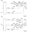
figure 12 is a schematic circuit diagram of three-way Doherty amplifier according to a first further alternative exemplary embodiment; and -
figure 13 is a schematic circuit diagram of a three-way Doherty amplifier according to a second further alternative exemplary embodiment. - A main principle according to embodiments of the invention disclosed herein is based on a combination of electrically connected coupled and single transmission lines in an output stage of a power amplifier comprising two or more amplifier stages providing phase shifted amplified outputs of an input signal. Coupled transmission lines are known for use as impedance transforming elements in impedance matching structures, but not as combining structures for load modulation power amplifiers such as Doherty or Chireix power amplifiers, where amplifier operation has to be guaranteed under dynamically varying load conditions.
-
Figure 6 illustrates a two-way symmetric Doherty power amplifier according to a first exemplary embodiment of the invention. As with the Doherty amplifier shown infigure 1 , the amplifier comprises first andsecond amplifier stages second amplifier stage 602 being provided with a phase-shifted version of the input signal. The outputs of theamplifier stages power combiner stage 603. Thepower combiner 603 comprises a pair of coupledtransmission lines 605, eachtransmission line - As used herein, the term coupled lines, or coupled transmission lines, refers to two transmission lines that share common electrical and magnetic field.
- An optional
third transmission line 606 with a characteristic impedance Z01 and a length of at least λ/4 is also shown connected between the second one 605b of the coupledpair 605 and theoutput load 604, which is also connected to the output of thesecond amplifier stage 602. The coupledlines 605 may be characterised by their even and odd mode impedances or alternatively by their geometrical dimensions. Thetransmission lines third transmission line 606 may also be implemented in a similar way. In alternative embodiments, the third transmission line may be absent, and replaced by a short circuit and the open end of the second coupledline 605b connected to ground. - As an illustrative example, the impedances of the
transmission lines - The performance of the coupled line Doherty power combiner of the embodiment in
figure 6 is shown infigure 7 , as compared to an equivalent conventional Doherty power combiner. The bandwidth of the combiner comprising a coupled pair of transmission lines at double load (indicated by the legend identified as Z100 infigure 7 , with "Z100 λ/4" indicating the conventional combiner and "Z100 cpl" with the coupled transmission lines) shows an improvement in the bandwidth at a VSWR of 1.05 from 0.85 f0 to around 1.15 f0, or a relative BW of 30 %, for a centre frequency f0 of 2GHz. This is a 50% effective increase of the BW compared with the conventional power combiner. The result of this is that the power amplifier performance at frequencies away from the centre frequency is improved. The centre frequency f0 of the power combiner may be other than 2GHz, which is shown infigure 7 by way of example only. -
Figure 8 shows the performance of theexemplary combiner 603 further optimized for a maximally flat response at double load by adjusting the parameters of the coupledlines transmission line 606. In this case the double load line bandwidth for a VSWR of 1.1 is from 0.6 f0 to 1.35 f0 (1.2 GHz to 2.7 GHz with f0=2GHz), equivalent to a relative bandwidth of 75%. For a VSWR of 1.05 the bandwidth is from 0.65 f0 to 1.3 f0 (1.3 GHz to 2.6 GHz for f0=2GHz), equivalent to a relative bandwidth of 65%. - As shown in the results in
figures 7 and 8 , the performance of theamplifier 600 with a nominal load will deteriorate and become comparable to the performance of the conventional combiner at double load. The overall performance of thepower amplifier 600 will however be improved, since most of the time the amplifier operates according to the double load line. - The optimal performance of different types of power amplifier may differ from case to case. In the case of a Chireix outphasing amplifier, the output is subject to much bigger load variations than with a two-way Doherty amplifier. The parameters of the coupled line combining structure to optimize the composite power amplifier performance according to predetermined criteria may calculated and adjusted accordingly, for example through the use of known computer simulation techniques.
- Illustrated in
figure 9 is apower amplifier 900 according to a second exemplary embodiment of the invention. Thepower amplifier 900 is in the form of a Chireix outphasing amplifier, having first and second amplifier stages 901, 902 with inputs connected to an SCS (Signal Component Separator)input stage 909, which performs signal processing of the input signal. Outputs of the amplifier stages 901, 902 are connected to apower combiner stage 903 comprising afirst pair 905 of coupled first andsecond transmission lines first amplifier stage 901 and anoutput load 904, asecond pair 907 of coupled third andfourth transmission lines second amplifier stage 902 and theoutput load 904. A second one 905b of thefirst pair 905 of coupled transmission lines is connected to theoutput load 904 via afifth transmission line 906 and a second one 907b of thesecond pair 907 of coupled transmission lines is connected to theoutput load 904 via asixth transmission line 908. - As with the Doherty amplifier embodiment of
figure 6 , the fifth andsixth transmission lines - The efficiency of the
combiner 903 of theamplifier 900 offigure 9 is shown as a function of outphasing angle infigure 10 , as compared with a conventional Chireix combiner. The results are shown at several different frequencies, ranging from 2 to 2.3 GHz. For outphasing angles exceeding 40 degrees, thecombiner 903 performance (illustrated by lines marked according to the legends CPL 2GHz, CPL 2.1GHz, CPL 2.2 GHz and CPL 2.3 GHz) demonstrates a significantly higher efficiency over the entire frequency band compared with the conventional combiner (illustrated by lines marked according to the legends Ch 2GHz, Ch 2.1 GHz, Ch 2.2 GHz and Ch 2.3 GHz), with the sole exception of thecentre frequency 2 GHz where the performance is roughly equal. - The results illustrated in
figure 11 show the case when thecombiner 903 is tuned for a flat frequency response. This illustrates that thecombiner 903 can handle a 10% bandwidth centred around 2 GHz with a minimal deterioration in efficiency. If some small loss of efficiency can be tolerated at small outphasing angles (which, according to the signal statistics, may occur at rare instances), the combiner can be successfully implemented using a relative bandwidth of more than 25%, resulting in a significant improvement in power amplifier performance. - Two further alternative exemplary embodiments of a three-way Doherty amplifier implementation are illustrated in
figures 12 and 13 , these embodiments being equivalent to three-way Doherty amplifiers described in further detail inWO 2009/081341 , but with the addition of coupled transmission lines connected between the outputs of further amplifier stages and the output load. According to a first alternative embodiment, shown infigure 12 , thepower amplifier 1200 comprises three amplifier stages including a firstmain amplifier stage 1201 and two further peak amplifier stages 1202a, 1202b. A coupled pair of first andsecond transmission lines 1205a, 1205b is connected between the output of thefirst amplifier 1201 and the output of the first peak amplifying stage 1202a and a second coupled pair of third andfourth transmission lines 1205c, 1205d is connected between the output of the second amplifier 1202a and theload 1204. As with the other embodiments described above, thesecond transmission line 1205b and the fourth transmission line 1205d are connected to theoutput load 1204 via fifth andsixth transmission lines second transmission lines 1205a, 1205b are connected to theoutput load 1204 via thethird transmission line 1205c. - In the alternative embodiment shown in
figure 13 , thepower amplifier 1300 also comprises three amplifier stages including a first main amplifier stage 1301 and two further peak amplifier stages 1302a, 1302b. A coupled pair of first andsecond transmission lines 1305a, 1305b is connected between the output of the first amplifier 1301 and theoutput load 1304, a second coupled pair of third andfourth transmission lines sixth transmission lines load 1304. The second andsixth transmission lines output load 1304 via seventh, andninth transmission lines fourth transmission line 1305d is connected to the output of the third amplifying stage 1302b via the eighttransmission line 1305h. Each of the second, sixth and ninth transmission lines is at least a quarter wavelength. The third andfourth transmission lines output load 1304 also via thefifth transmission line 1305e. The first to sixth transmission lines 1305a-f are preferably each a quarter wavelength in length. - Power amplifiers according to embodiments of the invention may be used to improve performance of contemporary high efficiency power amplifiers for use in telecommunication base stations using load modulation techniques. Doherty and Chireix outphasing power amplifier implementations may be particularly relevant where important power amplifier parameters such as gain, efficiency, linearity and output power need to be maintained over the entire operational frequency band, since the operational bandwidth of such amplifiers can be increased according to the embodiments disclosed herein.
- Other embodiments are also within the scope of the invention, which is to be defined by the following claims.
Claims (12)
- A power amplifier (600, 900) comprising an input connected to first and second amplifier stages (601, 602; 901, 902) and an output stage (603, 903) configured to combine phase shifted amplified outputs from the first and second amplifier stages (601, 602; 901, 902) and to provide an amplified signal at an output of the power amplifier (600, 900),
wherein the output stage (603, 903) comprises coupled first and second transmission lines (605a, 605b; 905a, 905b) connected between the output of the first amplifier stage (601; 901) and an output load connection. - The power amplifier (600) of claim 1 wherein the power amplifier is configured as a Doherty amplifier.
- The power amplifier (600) of claim 2 wherein the first transmission line (605a) is connected between the output of the first amplifier stage (601) and the output load connection, and the second transmission line (605b) is connected to the output of the second amplifier stage (602) and coupled to the first transmission line (605a).
- The power amplifier (600) of claim 3 wherein the first and second transmission lines (605a, 605b) have a length of a quarter of a wavelength of an operating frequency of the power amplifier (600).
- The power amplifier (600) of claim 4 wherein the second transmission line (605b) is connected to the output load connection via a third transmission line (606) having a length of at least a quarter wavelength of the operating frequency of the power amplifier (600).
- The power amplifier (600) of claim 4 or claim 5 wherein the operating frequency is within the range 1 to 3 GHz.
- The power amplifier (1200, 1300) of any one of claims 2 to 6 comprising:a third amplifier stage (1202b, 1302b) having an output connected to the output load connection; andcoupled third and fourth transmission lines (1205c, 1205d; 1305c, 1305d) connected between the output of the second amplifier stage (1202a) and the output load connection.
- The power amplifier (1300) of claim 7 comprising coupled fifth and sixth transmission lines (1305e, 1305f) connected between the output of the third (1302b) amplifier stage and the output load connection.
- The power amplifier (900) of claim 1 wherein the power amplifier is configured as a Chireix outphasing amplifier, the power amplifier comprising coupled third and fourth transmission lines (907a, 907b) connected between the output of the second amplifier stage (902) and the output load connection.
- The power amplifier (900) of claim 9 wherein the first to fourth transmission lines (905a, 905b, 907a, 907b) each have a length of a quarter of a wavelength of an operating frequency of the power amplifier.
- The power amplifier (900) of claim 10 wherein the second transmission line (905b) is connected to the output load connection via a fifth transmission line (906) and the fourth transmission line (907b) is connected to the output load connection via a sixth transmission line (908), the fifth and sixth transmission lines (906, 908) each having a length of at least a quarter wavelength of the operating frequency of the power amplifier.
- A method of operating a power amplifier (600, 900, 1200, 1300) according to any one of claims 1 to 11, the method comprising:receiving a signal at an input of the power amplifier;dividing the signal between the first and second amplifier stages (601, 602; 901, 902; 1201, 1202a; 1301, 1302a);amplifying the divided signal by the first and second amplifier stages;combining the resulting amplified signals from outputs of the first and second amplifiers in the output stage (603, 903); andproviding an amplified output signal at an output of the power amplifier.
Priority Applications (3)
| Application Number | Priority Date | Filing Date | Title |
|---|---|---|---|
| EP10250822.3A EP2383883B1 (en) | 2010-04-23 | 2010-04-23 | Power amplifier |
| US13/089,789 US8564367B2 (en) | 2010-04-23 | 2011-04-19 | Power amplifier |
| CN201110107268.1A CN102237852B (en) | 2010-04-23 | 2011-04-25 | Power amplifier |
Applications Claiming Priority (1)
| Application Number | Priority Date | Filing Date | Title |
|---|---|---|---|
| EP10250822.3A EP2383883B1 (en) | 2010-04-23 | 2010-04-23 | Power amplifier |
Publications (2)
| Publication Number | Publication Date |
|---|---|
| EP2383883A1 true EP2383883A1 (en) | 2011-11-02 |
| EP2383883B1 EP2383883B1 (en) | 2013-07-17 |
Family
ID=42629527
Family Applications (1)
| Application Number | Title | Priority Date | Filing Date |
|---|---|---|---|
| EP10250822.3A Active EP2383883B1 (en) | 2010-04-23 | 2010-04-23 | Power amplifier |
Country Status (3)
| Country | Link |
|---|---|
| US (1) | US8564367B2 (en) |
| EP (1) | EP2383883B1 (en) |
| CN (1) | CN102237852B (en) |
Cited By (8)
| Publication number | Priority date | Publication date | Assignee | Title |
|---|---|---|---|---|
| EP2621084A1 (en) * | 2012-01-24 | 2013-07-31 | System Engineering Solutions S.r.l. | Power amplifier with modified doherty topology |
| EP2698918A1 (en) * | 2012-08-14 | 2014-02-19 | Nxp B.V. | Amplifier circuit |
| WO2015057118A1 (en) * | 2013-10-18 | 2015-04-23 | Telefonaktiebolaget L M Ericsson (Publ) | Power amplifier for amplification of an input signal into an output signal |
| EP2876810A1 (en) * | 2013-11-22 | 2015-05-27 | Nxp B.V. | Doherty amplifier |
| JPWO2018109930A1 (en) * | 2016-12-16 | 2019-06-24 | 株式会社Wave Technology | Doherty amplifier |
| CN110011623A (en) * | 2019-03-28 | 2019-07-12 | 杭州电子科技大学温州研究院有限公司 | A kind of incorgruous power amplifier of dual band radio frequency |
| WO2022039640A1 (en) * | 2020-08-19 | 2022-02-24 | Telefonaktiebolaget Lm Ericsson (Publ) | Power combiner for amplifier arrangement |
| JPWO2023127435A1 (en) * | 2021-12-28 | 2023-07-06 |
Families Citing this family (29)
| Publication number | Priority date | Publication date | Assignee | Title |
|---|---|---|---|---|
| CN107501244B (en) | 2011-11-22 | 2022-05-03 | 出光兴产株式会社 | Aromatic heterocyclic derivative, material for organic electroluminescent element, and organic electroluminescent element |
| CN103178785B (en) * | 2011-12-20 | 2016-08-03 | 上海贝尔股份有限公司 | A kind of Novel Doherty power amplifier |
| US8717099B2 (en) * | 2012-03-16 | 2014-05-06 | Infineon Technologies Ag | Wideband doherty amplifier circuit with peaking impedance absorption |
| US8779856B2 (en) * | 2012-10-31 | 2014-07-15 | Infineon Technologies Ag | Doherty amplifier circuit with phase-controlled load modulation |
| WO2014075735A1 (en) * | 2012-11-16 | 2014-05-22 | Nokia Solutions And Networks Oy | High efficiency high peak-to-average ratio broadband 3-way power amplifier |
| US9431969B2 (en) * | 2012-12-11 | 2016-08-30 | Rf Micro Devices, Inc. | Doherty power amplifier with tunable impedance load |
| US9397617B2 (en) | 2013-06-25 | 2016-07-19 | Rf Micro Devices, Inc. | Multi-broadband Doherty power amplifier |
| EP2819304B1 (en) | 2013-06-26 | 2018-12-19 | Ampleon Netherlands B.V. | Doherty amplifier |
| US9948243B2 (en) | 2013-09-30 | 2018-04-17 | Qorvo Us, Inc. | Reconfigurable load modulation amplifier |
| US9484865B2 (en) | 2013-09-30 | 2016-11-01 | Qorvo Us, Inc. | Reconfigurable load modulation amplifier |
| EP2869463B1 (en) * | 2013-10-31 | 2016-01-06 | Samba Holdco Netherlands B.V. | Doherty amplifier structure |
| CN104716911A (en) * | 2013-12-13 | 2015-06-17 | 中兴通讯股份有限公司 | Radio frequency power amplifier, base station and impedance adjusting method |
| US20150200631A1 (en) * | 2014-01-15 | 2015-07-16 | Alcatel-Lucent Canada Inc. | Dual-band doherty combiner/impedance transformer circuit and doherty power amplifier including the same |
| US9369095B2 (en) | 2014-01-27 | 2016-06-14 | Rf Micro Devices, Inc. | Unbalanced linear power amplifier |
| CN104917472B (en) * | 2014-03-10 | 2019-04-16 | 中兴通讯股份有限公司 | Power amplifier circuit, power amplifier device and broadband matching method thereof |
| WO2015139745A1 (en) * | 2014-03-19 | 2015-09-24 | Telefonaktiebolaget L M Ericsson (Publ) | Amplifier circuit and method |
| WO2016056953A1 (en) * | 2014-10-06 | 2016-04-14 | Telefonaktiebolaget L M Ericsson (Publ) | Amplifier circuit and method |
| CN104716913B (en) * | 2015-04-07 | 2018-07-27 | 清华大学 | Load modulation power amplifier |
| US9634618B2 (en) * | 2015-07-20 | 2017-04-25 | City University Of Hong Kong | Impedance matching arrangement for an amplifier |
| KR102093658B1 (en) * | 2015-07-28 | 2020-03-26 | 후아웨이 테크놀러지 컴퍼니 리미티드 | Power amplifier, power amplification method and power amplification control device and method |
| US9882535B2 (en) * | 2016-06-28 | 2018-01-30 | Infineon Technologies Ag | Doherty-Chireix combined amplifier |
| US9948246B1 (en) * | 2016-10-18 | 2018-04-17 | Mitsubishi Electric Research Laboratories, Inc. | Impedance flattening network for high efficiency wideband doherty power amplifier |
| JP2019057809A (en) * | 2017-09-20 | 2019-04-11 | 株式会社東芝 | Amplifier and transmitter |
| US10601375B2 (en) * | 2017-10-03 | 2020-03-24 | Sumitomo Electronic Devices Innovations, Inc. | Modified three-stage doherty amplifier |
| NL2021613B1 (en) * | 2018-09-12 | 2020-05-06 | Ampleon Netherlands Bv | Impedance control unit |
| CN110011621B (en) * | 2019-03-28 | 2023-07-28 | 杭州电子科技大学温州研究院有限公司 | A High Backoff Range RF Power Amplifier Integrated Anisotropy and Doherty Structure |
| US11398798B2 (en) | 2020-03-02 | 2022-07-26 | Skyworks Solutions, Inc. | Doherty power amplifiers with coupled line combiners |
| US12206363B2 (en) | 2021-05-26 | 2025-01-21 | Skyworks Solutions, Inc. | Load modulated power amplifiers |
| JP7651996B2 (en) * | 2021-07-20 | 2025-03-27 | 住友電気工業株式会社 | Outphasing Amplifier |
Citations (7)
| Publication number | Priority date | Publication date | Assignee | Title |
|---|---|---|---|---|
| WO1997020385A1 (en) * | 1995-11-30 | 1997-06-05 | Motorola Inc. | Doherty-type amplifier and tuning method |
| WO1999052206A1 (en) * | 1998-04-02 | 1999-10-14 | Ericsson, Inc. | Hybrid chireix/doherty amplifiers power waveform synthesis |
| WO2001003289A1 (en) * | 1999-07-06 | 2001-01-11 | Motorola Inc. | Power amplifier for efficiently amplifying linearly modulated signals |
| US6329877B1 (en) * | 1999-06-25 | 2001-12-11 | Agere Systems Guardian Corp. | Efficient power amplifier |
| WO2004057755A1 (en) * | 2002-12-19 | 2004-07-08 | Telefonaktiebolaget Lm Ericsson | Composite amplifier structure |
| WO2004088837A2 (en) * | 2003-03-28 | 2004-10-14 | Andrew Corporation | Doherty amplifier with output hybrid coupler |
| WO2009081341A1 (en) | 2007-12-21 | 2009-07-02 | Nxp B.V. | 3-way doherty amplifier with minimum output network |
Family Cites Families (2)
| Publication number | Priority date | Publication date | Assignee | Title |
|---|---|---|---|---|
| KR100814415B1 (en) * | 2007-02-14 | 2008-03-18 | 포항공과대학교 산학협력단 | High Efficiency Doherty Power Amplifier Using Harmonic Control Circuit |
| US8228123B2 (en) * | 2007-08-29 | 2012-07-24 | Nxp B.V. | Integrated Doherty amplifier |
-
2010
- 2010-04-23 EP EP10250822.3A patent/EP2383883B1/en active Active
-
2011
- 2011-04-19 US US13/089,789 patent/US8564367B2/en active Active
- 2011-04-25 CN CN201110107268.1A patent/CN102237852B/en active Active
Patent Citations (7)
| Publication number | Priority date | Publication date | Assignee | Title |
|---|---|---|---|---|
| WO1997020385A1 (en) * | 1995-11-30 | 1997-06-05 | Motorola Inc. | Doherty-type amplifier and tuning method |
| WO1999052206A1 (en) * | 1998-04-02 | 1999-10-14 | Ericsson, Inc. | Hybrid chireix/doherty amplifiers power waveform synthesis |
| US6329877B1 (en) * | 1999-06-25 | 2001-12-11 | Agere Systems Guardian Corp. | Efficient power amplifier |
| WO2001003289A1 (en) * | 1999-07-06 | 2001-01-11 | Motorola Inc. | Power amplifier for efficiently amplifying linearly modulated signals |
| WO2004057755A1 (en) * | 2002-12-19 | 2004-07-08 | Telefonaktiebolaget Lm Ericsson | Composite amplifier structure |
| WO2004088837A2 (en) * | 2003-03-28 | 2004-10-14 | Andrew Corporation | Doherty amplifier with output hybrid coupler |
| WO2009081341A1 (en) | 2007-12-21 | 2009-07-02 | Nxp B.V. | 3-way doherty amplifier with minimum output network |
Non-Patent Citations (5)
| Title |
|---|
| EL-ASMAR M ET AL: "Investigation of Chireix PA performances by testing one branch variable load amplifier", ADVANCES IN COMPUTATIONAL TOOLS FOR ENGINEERING APPLICATIONS, 2009. ACTEA '09. INTERNATIONAL CONFERENCE ON, IEEE, PISCATAWAY, NJ, USA, 15 July 2009 (2009-07-15), pages 279 - 283, XP031523200, ISBN: 978-1-4244-3833-4 * |
| GERHARD W ET AL: "Improvement of power amplifier efficiency by reactive Chireix combining, power back-off and differential phase adjustment", MICROWAVE SYMPOSIUM DIGEST, 2006. IEEE MTT-S INTERNATIONAL, IEEE, PI, 1 June 2006 (2006-06-01), pages 1887 - 1890, XP031018860, ISBN: 978-0-7803-9541-1, DOI: 10.1109/MWSYM.2006.249783 * |
| HONGTAO XU ET AL: "A highly linear 25dBm outphasing power amplifier in 32nm CMOS for WLAN application", ESSCIRC, 2010 PROCEEDINGS OF THE, IEEE, PISCATAWAY, NJ, USA, 14 September 2010 (2010-09-14), pages 306 - 309, XP031788370, ISBN: 978-1-4244-6662-7 * |
| POITAU G ET AL: "Experimental characterization of LINC outphasing combiners - efficiency and linearity", RADIO AND WIRELESS CONFERENCE, 2004 IEEE ATLANTA, GA, USA 19-22 SEPT. 2004, PISCATAWAY, NJ, USA,IEEE, PISCATAWAY, NJ, USA, 19 September 2004 (2004-09-19), pages 87 - 90, XP010764555, ISBN: 978-0-7803-8451-4, DOI: 10.1109/RAWCON.2004.1389078 * |
| YIJUN ZHOU ET AL: "A distributed active transformer coupled outphasing power combiner", MICROWAVE CONFERENCE, 2009. APMC 2009. ASIA PACIFIC, IEEE, PISCATAWAY, NJ, USA, 7 December 2009 (2009-12-07), pages 2565 - 2568, XP031614035, ISBN: 978-1-4244-2801-4 * |
Cited By (11)
| Publication number | Priority date | Publication date | Assignee | Title |
|---|---|---|---|---|
| EP2621084A1 (en) * | 2012-01-24 | 2013-07-31 | System Engineering Solutions S.r.l. | Power amplifier with modified doherty topology |
| EP2698918A1 (en) * | 2012-08-14 | 2014-02-19 | Nxp B.V. | Amplifier circuit |
| WO2015057118A1 (en) * | 2013-10-18 | 2015-04-23 | Telefonaktiebolaget L M Ericsson (Publ) | Power amplifier for amplification of an input signal into an output signal |
| US9906193B2 (en) | 2013-10-18 | 2018-02-27 | Telefonaktiebolaget Lm Ericsson (Publ) | Power amplifier for amplification of an input signal into an output signal |
| EP2876810A1 (en) * | 2013-11-22 | 2015-05-27 | Nxp B.V. | Doherty amplifier |
| JPWO2018109930A1 (en) * | 2016-12-16 | 2019-06-24 | 株式会社Wave Technology | Doherty amplifier |
| CN110011623A (en) * | 2019-03-28 | 2019-07-12 | 杭州电子科技大学温州研究院有限公司 | A kind of incorgruous power amplifier of dual band radio frequency |
| WO2022039640A1 (en) * | 2020-08-19 | 2022-02-24 | Telefonaktiebolaget Lm Ericsson (Publ) | Power combiner for amplifier arrangement |
| JPWO2023127435A1 (en) * | 2021-12-28 | 2023-07-06 | ||
| WO2023127435A1 (en) * | 2021-12-28 | 2023-07-06 | 株式会社村田製作所 | Power amplification circuit and power amplification module |
| JP7666651B2 (en) | 2021-12-28 | 2025-04-22 | 株式会社村田製作所 | Power amplifier circuit, power amplifier module |
Also Published As
| Publication number | Publication date |
|---|---|
| CN102237852B (en) | 2014-12-31 |
| US8564367B2 (en) | 2013-10-22 |
| US20120126890A1 (en) | 2012-05-24 |
| CN102237852A (en) | 2011-11-09 |
| EP2383883B1 (en) | 2013-07-17 |
Similar Documents
| Publication | Publication Date | Title |
|---|---|---|
| EP2383883B1 (en) | Power amplifier | |
| JP4486620B2 (en) | Multiband Doherty amplifier | |
| US9614480B2 (en) | Wide-band multi stage doherty power amplifier | |
| US7262656B2 (en) | Circuit for parallel operation of Doherty amplifiers | |
| JP5905459B2 (en) | High frequency power amplifier with Doherty extension | |
| EP1912328B1 (en) | Highly efficient amplifier | |
| CN102137518A (en) | Doherty power amplifier and multi-frequency band signal parameter adjusting device | |
| JP6608959B2 (en) | Composite power amplifier | |
| US10084413B2 (en) | Doherty power amplifier and transmitter | |
| WO2009131138A1 (en) | Amplifier | |
| JP5678768B2 (en) | Amplifier | |
| JP2006332829A (en) | amplifier | |
| KR101066640B1 (en) | 2-stage connected bias mixed power amplifier | |
| EP2413498A1 (en) | Doherty amplifier | |
| US9054647B2 (en) | High frequency power amplifier | |
| KR101094067B1 (en) | Class F and Inverse Class F Doherty Amplifiers | |
| CN112425069A (en) | Power oscillator using gallium nitride power amplifier | |
| JP2017169200A (en) | Directional coupler and power splitter made therefrom | |
| JP5390495B2 (en) | High frequency amplifier | |
| EP2761740B1 (en) | Amplifying system | |
| JP6649217B2 (en) | Received signal amplifier and transceiver | |
| US20040090271A1 (en) | Variable gain amplifier for high frequency band using microstrip hybrid | |
| KR20210100451A (en) | Radial combiner | |
| JP2005151401A (en) | Feed-forward power amplifier |
Legal Events
| Date | Code | Title | Description |
|---|---|---|---|
| AK | Designated contracting states |
Kind code of ref document: A1 Designated state(s): AT BE BG CH CY CZ DE DK EE ES FI FR GB GR HR HU IE IS IT LI LT LU LV MC MK MT NL NO PL PT RO SE SI SK SM TR |
|
| AX | Request for extension of the european patent |
Extension state: AL BA ME RS |
|
| PUAI | Public reference made under article 153(3) epc to a published international application that has entered the european phase |
Free format text: ORIGINAL CODE: 0009012 |
|
| 17P | Request for examination filed |
Effective date: 20120502 |
|
| REG | Reference to a national code |
Ref country code: DE Ref legal event code: R079 Ref document number: 602010008599 Country of ref document: DE Free format text: PREVIOUS MAIN CLASS: H03F0001020000 Ipc: H03F0003600000 |
|
| GRAP | Despatch of communication of intention to grant a patent |
Free format text: ORIGINAL CODE: EPIDOSNIGR1 |
|
| RIC1 | Information provided on ipc code assigned before grant |
Ipc: H03F 3/60 20060101AFI20130226BHEP Ipc: H03F 1/02 20060101ALI20130226BHEP |
|
| GRAS | Grant fee paid |
Free format text: ORIGINAL CODE: EPIDOSNIGR3 |
|
| GRAA | (expected) grant |
Free format text: ORIGINAL CODE: 0009210 |
|
| AK | Designated contracting states |
Kind code of ref document: B1 Designated state(s): AT BE BG CH CY CZ DE DK EE ES FI FR GB GR HR HU IE IS IT LI LT LU LV MC MK MT NL NO PL PT RO SE SI SK SM TR |
|
| REG | Reference to a national code |
Ref country code: GB Ref legal event code: FG4D |
|
| REG | Reference to a national code |
Ref country code: CH Ref legal event code: EP |
|
| REG | Reference to a national code |
Ref country code: IE Ref legal event code: FG4D |
|
| REG | Reference to a national code |
Ref country code: AT Ref legal event code: REF Ref document number: 622738 Country of ref document: AT Kind code of ref document: T Effective date: 20130815 |
|
| REG | Reference to a national code |
Ref country code: DE Ref legal event code: R096 Ref document number: 602010008599 Country of ref document: DE Effective date: 20130912 |
|
| REG | Reference to a national code |
Ref country code: AT Ref legal event code: MK05 Ref document number: 622738 Country of ref document: AT Kind code of ref document: T Effective date: 20130717 |
|
| REG | Reference to a national code |
Ref country code: NL Ref legal event code: VDEP Effective date: 20130717 |
|
| REG | Reference to a national code |
Ref country code: LT Ref legal event code: MG4D |
|
| PG25 | Lapsed in a contracting state [announced via postgrant information from national office to epo] |
Ref country code: SE Free format text: LAPSE BECAUSE OF FAILURE TO SUBMIT A TRANSLATION OF THE DESCRIPTION OR TO PAY THE FEE WITHIN THE PRESCRIBED TIME-LIMIT Effective date: 20130717 Ref country code: AT Free format text: LAPSE BECAUSE OF FAILURE TO SUBMIT A TRANSLATION OF THE DESCRIPTION OR TO PAY THE FEE WITHIN THE PRESCRIBED TIME-LIMIT Effective date: 20130717 Ref country code: LT Free format text: LAPSE BECAUSE OF FAILURE TO SUBMIT A TRANSLATION OF THE DESCRIPTION OR TO PAY THE FEE WITHIN THE PRESCRIBED TIME-LIMIT Effective date: 20130717 Ref country code: BE Free format text: LAPSE BECAUSE OF FAILURE TO SUBMIT A TRANSLATION OF THE DESCRIPTION OR TO PAY THE FEE WITHIN THE PRESCRIBED TIME-LIMIT Effective date: 20130717 Ref country code: NO Free format text: LAPSE BECAUSE OF FAILURE TO SUBMIT A TRANSLATION OF THE DESCRIPTION OR TO PAY THE FEE WITHIN THE PRESCRIBED TIME-LIMIT Effective date: 20131017 Ref country code: IS Free format text: LAPSE BECAUSE OF FAILURE TO SUBMIT A TRANSLATION OF THE DESCRIPTION OR TO PAY THE FEE WITHIN THE PRESCRIBED TIME-LIMIT Effective date: 20131117 Ref country code: CY Free format text: LAPSE BECAUSE OF FAILURE TO SUBMIT A TRANSLATION OF THE DESCRIPTION OR TO PAY THE FEE WITHIN THE PRESCRIBED TIME-LIMIT Effective date: 20130724 Ref country code: PT Free format text: LAPSE BECAUSE OF FAILURE TO SUBMIT A TRANSLATION OF THE DESCRIPTION OR TO PAY THE FEE WITHIN THE PRESCRIBED TIME-LIMIT Effective date: 20131118 Ref country code: HR Free format text: LAPSE BECAUSE OF FAILURE TO SUBMIT A TRANSLATION OF THE DESCRIPTION OR TO PAY THE FEE WITHIN THE PRESCRIBED TIME-LIMIT Effective date: 20130717 |
|
| PG25 | Lapsed in a contracting state [announced via postgrant information from national office to epo] |
Ref country code: GR Free format text: LAPSE BECAUSE OF FAILURE TO SUBMIT A TRANSLATION OF THE DESCRIPTION OR TO PAY THE FEE WITHIN THE PRESCRIBED TIME-LIMIT Effective date: 20131018 Ref country code: PL Free format text: LAPSE BECAUSE OF FAILURE TO SUBMIT A TRANSLATION OF THE DESCRIPTION OR TO PAY THE FEE WITHIN THE PRESCRIBED TIME-LIMIT Effective date: 20130717 Ref country code: NL Free format text: LAPSE BECAUSE OF FAILURE TO SUBMIT A TRANSLATION OF THE DESCRIPTION OR TO PAY THE FEE WITHIN THE PRESCRIBED TIME-LIMIT Effective date: 20130717 Ref country code: FI Free format text: LAPSE BECAUSE OF FAILURE TO SUBMIT A TRANSLATION OF THE DESCRIPTION OR TO PAY THE FEE WITHIN THE PRESCRIBED TIME-LIMIT Effective date: 20130717 Ref country code: SI Free format text: LAPSE BECAUSE OF FAILURE TO SUBMIT A TRANSLATION OF THE DESCRIPTION OR TO PAY THE FEE WITHIN THE PRESCRIBED TIME-LIMIT Effective date: 20130717 Ref country code: ES Free format text: LAPSE BECAUSE OF FAILURE TO SUBMIT A TRANSLATION OF THE DESCRIPTION OR TO PAY THE FEE WITHIN THE PRESCRIBED TIME-LIMIT Effective date: 20131028 Ref country code: LV Free format text: LAPSE BECAUSE OF FAILURE TO SUBMIT A TRANSLATION OF THE DESCRIPTION OR TO PAY THE FEE WITHIN THE PRESCRIBED TIME-LIMIT Effective date: 20130717 |
|
| PG25 | Lapsed in a contracting state [announced via postgrant information from national office to epo] |
Ref country code: CY Free format text: LAPSE BECAUSE OF FAILURE TO SUBMIT A TRANSLATION OF THE DESCRIPTION OR TO PAY THE FEE WITHIN THE PRESCRIBED TIME-LIMIT Effective date: 20130717 |
|
| PG25 | Lapsed in a contracting state [announced via postgrant information from national office to epo] |
Ref country code: CZ Free format text: LAPSE BECAUSE OF FAILURE TO SUBMIT A TRANSLATION OF THE DESCRIPTION OR TO PAY THE FEE WITHIN THE PRESCRIBED TIME-LIMIT Effective date: 20130717 Ref country code: RO Free format text: LAPSE BECAUSE OF FAILURE TO SUBMIT A TRANSLATION OF THE DESCRIPTION OR TO PAY THE FEE WITHIN THE PRESCRIBED TIME-LIMIT Effective date: 20130717 Ref country code: EE Free format text: LAPSE BECAUSE OF FAILURE TO SUBMIT A TRANSLATION OF THE DESCRIPTION OR TO PAY THE FEE WITHIN THE PRESCRIBED TIME-LIMIT Effective date: 20130717 Ref country code: DK Free format text: LAPSE BECAUSE OF FAILURE TO SUBMIT A TRANSLATION OF THE DESCRIPTION OR TO PAY THE FEE WITHIN THE PRESCRIBED TIME-LIMIT Effective date: 20130717 Ref country code: SK Free format text: LAPSE BECAUSE OF FAILURE TO SUBMIT A TRANSLATION OF THE DESCRIPTION OR TO PAY THE FEE WITHIN THE PRESCRIBED TIME-LIMIT Effective date: 20130717 |
|
| PLBE | No opposition filed within time limit |
Free format text: ORIGINAL CODE: 0009261 |
|
| STAA | Information on the status of an ep patent application or granted ep patent |
Free format text: STATUS: NO OPPOSITION FILED WITHIN TIME LIMIT |
|
| PG25 | Lapsed in a contracting state [announced via postgrant information from national office to epo] |
Ref country code: IT Free format text: LAPSE BECAUSE OF FAILURE TO SUBMIT A TRANSLATION OF THE DESCRIPTION OR TO PAY THE FEE WITHIN THE PRESCRIBED TIME-LIMIT Effective date: 20130717 |
|
| 26N | No opposition filed |
Effective date: 20140422 |
|
| REG | Reference to a national code |
Ref country code: DE Ref legal event code: R097 Ref document number: 602010008599 Country of ref document: DE Effective date: 20140422 |
|
| PG25 | Lapsed in a contracting state [announced via postgrant information from national office to epo] |
Ref country code: MC Free format text: LAPSE BECAUSE OF FAILURE TO SUBMIT A TRANSLATION OF THE DESCRIPTION OR TO PAY THE FEE WITHIN THE PRESCRIBED TIME-LIMIT Effective date: 20130717 Ref country code: LU Free format text: LAPSE BECAUSE OF FAILURE TO SUBMIT A TRANSLATION OF THE DESCRIPTION OR TO PAY THE FEE WITHIN THE PRESCRIBED TIME-LIMIT Effective date: 20140423 |
|
| REG | Reference to a national code |
Ref country code: CH Ref legal event code: PL |
|
| GBPC | Gb: european patent ceased through non-payment of renewal fee |
Effective date: 20140423 |
|
| REG | Reference to a national code |
Ref country code: IE Ref legal event code: MM4A |
|
| PG25 | Lapsed in a contracting state [announced via postgrant information from national office to epo] |
Ref country code: LI Free format text: LAPSE BECAUSE OF NON-PAYMENT OF DUE FEES Effective date: 20140430 Ref country code: GB Free format text: LAPSE BECAUSE OF NON-PAYMENT OF DUE FEES Effective date: 20140423 Ref country code: CH Free format text: LAPSE BECAUSE OF NON-PAYMENT OF DUE FEES Effective date: 20140430 |
|
| REG | Reference to a national code |
Ref country code: FR Ref legal event code: PLFP Year of fee payment: 6 |
|
| PG25 | Lapsed in a contracting state [announced via postgrant information from national office to epo] |
Ref country code: IE Free format text: LAPSE BECAUSE OF NON-PAYMENT OF DUE FEES Effective date: 20140423 |
|
| REG | Reference to a national code |
Ref country code: FR Ref legal event code: TP Owner name: SAMBA HOLDCO NETHERLANDS BV, NL Effective date: 20150930 |
|
| REG | Reference to a national code |
Ref country code: DE Ref legal event code: R081 Ref document number: 602010008599 Country of ref document: DE Owner name: SAMBA HOLDCO NETHERLANDS B.V., NL Free format text: FORMER OWNER: NXP B.V., EINDHOVEN, NL Ref country code: DE Ref legal event code: R081 Ref document number: 602010008599 Country of ref document: DE Owner name: AMPLEON NETHERLANDS B.V., NL Free format text: FORMER OWNER: NXP B.V., EINDHOVEN, NL |
|
| REG | Reference to a national code |
Ref country code: DE Ref legal event code: R081 Ref document number: 602010008599 Country of ref document: DE Owner name: AMPLEON NETHERLANDS B.V., NL Free format text: FORMER OWNER: SAMBA HOLDCO NETHERLANDS B.V., EINDHOVEN, NL |
|
| PG25 | Lapsed in a contracting state [announced via postgrant information from national office to epo] |
Ref country code: MT Free format text: LAPSE BECAUSE OF FAILURE TO SUBMIT A TRANSLATION OF THE DESCRIPTION OR TO PAY THE FEE WITHIN THE PRESCRIBED TIME-LIMIT Effective date: 20130717 |
|
| REG | Reference to a national code |
Ref country code: FR Ref legal event code: PLFP Year of fee payment: 7 |
|
| PG25 | Lapsed in a contracting state [announced via postgrant information from national office to epo] |
Ref country code: SM Free format text: LAPSE BECAUSE OF FAILURE TO SUBMIT A TRANSLATION OF THE DESCRIPTION OR TO PAY THE FEE WITHIN THE PRESCRIBED TIME-LIMIT Effective date: 20130717 |
|
| PG25 | Lapsed in a contracting state [announced via postgrant information from national office to epo] |
Ref country code: BG Free format text: LAPSE BECAUSE OF FAILURE TO SUBMIT A TRANSLATION OF THE DESCRIPTION OR TO PAY THE FEE WITHIN THE PRESCRIBED TIME-LIMIT Effective date: 20130717 |
|
| PG25 | Lapsed in a contracting state [announced via postgrant information from national office to epo] |
Ref country code: TR Free format text: LAPSE BECAUSE OF FAILURE TO SUBMIT A TRANSLATION OF THE DESCRIPTION OR TO PAY THE FEE WITHIN THE PRESCRIBED TIME-LIMIT Effective date: 20130717 Ref country code: HU Free format text: LAPSE BECAUSE OF FAILURE TO SUBMIT A TRANSLATION OF THE DESCRIPTION OR TO PAY THE FEE WITHIN THE PRESCRIBED TIME-LIMIT; INVALID AB INITIO Effective date: 20100423 |
|
| REG | Reference to a national code |
Ref country code: FR Ref legal event code: CA Effective date: 20160721 Ref country code: FR Ref legal event code: CD Owner name: AMPLEON NETHERLANDS B.V., NL Effective date: 20160721 |
|
| REG | Reference to a national code |
Ref country code: FR Ref legal event code: PLFP Year of fee payment: 8 |
|
| REG | Reference to a national code |
Ref country code: FR Ref legal event code: PLFP Year of fee payment: 9 |
|
| PG25 | Lapsed in a contracting state [announced via postgrant information from national office to epo] |
Ref country code: MK Free format text: LAPSE BECAUSE OF FAILURE TO SUBMIT A TRANSLATION OF THE DESCRIPTION OR TO PAY THE FEE WITHIN THE PRESCRIBED TIME-LIMIT Effective date: 20130717 |
|
| P01 | Opt-out of the competence of the unified patent court (upc) registered |
Effective date: 20230526 |
|
| PGFP | Annual fee paid to national office [announced via postgrant information from national office to epo] |
Ref country code: FR Payment date: 20230425 Year of fee payment: 14 |
|
| PG25 | Lapsed in a contracting state [announced via postgrant information from national office to epo] |
Ref country code: FR Free format text: LAPSE BECAUSE OF NON-PAYMENT OF DUE FEES Effective date: 20240430 |
|
| PG25 | Lapsed in a contracting state [announced via postgrant information from national office to epo] |
Ref country code: FR Free format text: LAPSE BECAUSE OF NON-PAYMENT OF DUE FEES Effective date: 20240430 |
|
| PGFP | Annual fee paid to national office [announced via postgrant information from national office to epo] |
Ref country code: DE Payment date: 20250429 Year of fee payment: 16 |