EP2380412B1 - Methods and apparatus for dual confinement and ultra-high pressure in an adjustable gap plasma chamber - Google Patents
Methods and apparatus for dual confinement and ultra-high pressure in an adjustable gap plasma chamber Download PDFInfo
- Publication number
- EP2380412B1 EP2380412B1 EP09837887.0A EP09837887A EP2380412B1 EP 2380412 B1 EP2380412 B1 EP 2380412B1 EP 09837887 A EP09837887 A EP 09837887A EP 2380412 B1 EP2380412 B1 EP 2380412B1
- Authority
- EP
- European Patent Office
- Prior art keywords
- upper electrode
- gap
- lower electrode
- plasma processing
- electrode
- Prior art date
- Legal status (The legal status is an assumption and is not a legal conclusion. Google has not performed a legal analysis and makes no representation as to the accuracy of the status listed.)
- Active
Links
- 238000000034 method Methods 0.000 title claims description 26
- 230000009977 dual effect Effects 0.000 title 1
- 230000002093 peripheral effect Effects 0.000 claims description 24
- 239000000758 substrate Substances 0.000 claims description 22
- 230000008569 process Effects 0.000 claims description 11
- 230000008878 coupling Effects 0.000 claims description 7
- 238000010168 coupling process Methods 0.000 claims description 7
- 238000005859 coupling reaction Methods 0.000 claims description 7
- 239000010453 quartz Substances 0.000 claims description 7
- VYPSYNLAJGMNEJ-UHFFFAOYSA-N silicon dioxide Inorganic materials O=[Si]=O VYPSYNLAJGMNEJ-UHFFFAOYSA-N 0.000 claims description 7
- 230000008859 change Effects 0.000 claims description 3
- 230000007246 mechanism Effects 0.000 claims description 3
- 230000002459 sustained effect Effects 0.000 description 6
- 238000004519 manufacturing process Methods 0.000 description 4
- 239000004065 semiconductor Substances 0.000 description 4
- 238000011144 upstream manufacturing Methods 0.000 description 3
- 230000004075 alteration Effects 0.000 description 2
- 238000001020 plasma etching Methods 0.000 description 2
- XAGFODPZIPBFFR-UHFFFAOYSA-N aluminium Chemical compound [Al] XAGFODPZIPBFFR-UHFFFAOYSA-N 0.000 description 1
- 229910052782 aluminium Inorganic materials 0.000 description 1
- 230000002860 competitive effect Effects 0.000 description 1
- 238000005516 engineering process Methods 0.000 description 1
- 238000005530 etching Methods 0.000 description 1
- 230000006872 improvement Effects 0.000 description 1
- 238000009616 inductively coupled plasma Methods 0.000 description 1
- 239000012212 insulator Substances 0.000 description 1
- 238000004886 process control Methods 0.000 description 1
- 230000000284 resting effect Effects 0.000 description 1
Images

Classifications
-
- H—ELECTRICITY
- H01—ELECTRIC ELEMENTS
- H01J—ELECTRIC DISCHARGE TUBES OR DISCHARGE LAMPS
- H01J37/00—Discharge tubes with provision for introducing objects or material to be exposed to the discharge, e.g. for the purpose of examination or processing thereof
- H01J37/32—Gas-filled discharge tubes
- H01J37/32009—Arrangements for generation of plasma specially adapted for examination or treatment of objects, e.g. plasma sources
- H01J37/32082—Radio frequency generated discharge
- H01J37/32091—Radio frequency generated discharge the radio frequency energy being capacitively coupled to the plasma
-
- H—ELECTRICITY
- H01—ELECTRIC ELEMENTS
- H01J—ELECTRIC DISCHARGE TUBES OR DISCHARGE LAMPS
- H01J37/00—Discharge tubes with provision for introducing objects or material to be exposed to the discharge, e.g. for the purpose of examination or processing thereof
- H01J37/32—Gas-filled discharge tubes
- H01J37/32431—Constructional details of the reactor
- H01J37/3244—Gas supply means
- H01J37/32449—Gas control, e.g. control of the gas flow
-
- H—ELECTRICITY
- H01—ELECTRIC ELEMENTS
- H01J—ELECTRIC DISCHARGE TUBES OR DISCHARGE LAMPS
- H01J37/00—Discharge tubes with provision for introducing objects or material to be exposed to the discharge, e.g. for the purpose of examination or processing thereof
- H01J37/32—Gas-filled discharge tubes
- H01J37/32431—Constructional details of the reactor
- H01J37/32532—Electrodes
- H01J37/32541—Shape
-
- H—ELECTRICITY
- H01—ELECTRIC ELEMENTS
- H01J—ELECTRIC DISCHARGE TUBES OR DISCHARGE LAMPS
- H01J37/00—Discharge tubes with provision for introducing objects or material to be exposed to the discharge, e.g. for the purpose of examination or processing thereof
- H01J37/32—Gas-filled discharge tubes
- H01J37/32431—Constructional details of the reactor
- H01J37/32532—Electrodes
- H01J37/32568—Relative arrangement or disposition of electrodes; moving means
-
- H—ELECTRICITY
- H01—ELECTRIC ELEMENTS
- H01J—ELECTRIC DISCHARGE TUBES OR DISCHARGE LAMPS
- H01J37/00—Discharge tubes with provision for introducing objects or material to be exposed to the discharge, e.g. for the purpose of examination or processing thereof
- H01J37/32—Gas-filled discharge tubes
- H01J37/32431—Constructional details of the reactor
- H01J37/32623—Mechanical discharge control means
- H01J37/32642—Focus rings
-
- H—ELECTRICITY
- H01—ELECTRIC ELEMENTS
- H01J—ELECTRIC DISCHARGE TUBES OR DISCHARGE LAMPS
- H01J37/00—Discharge tubes with provision for introducing objects or material to be exposed to the discharge, e.g. for the purpose of examination or processing thereof
- H01J37/32—Gas-filled discharge tubes
- H01J37/32431—Constructional details of the reactor
- H01J37/32798—Further details of plasma apparatus not provided for in groups H01J37/3244 - H01J37/32788; special provisions for cleaning or maintenance of the apparatus
- H01J37/32816—Pressure
-
- H—ELECTRICITY
- H01—ELECTRIC ELEMENTS
- H01J—ELECTRIC DISCHARGE TUBES OR DISCHARGE LAMPS
- H01J37/00—Discharge tubes with provision for introducing objects or material to be exposed to the discharge, e.g. for the purpose of examination or processing thereof
- H01J37/32—Gas-filled discharge tubes
- H01J37/32917—Plasma diagnostics
- H01J37/3299—Feedback systems
-
- H—ELECTRICITY
- H01—ELECTRIC ELEMENTS
- H01L—SEMICONDUCTOR DEVICES NOT COVERED BY CLASS H10
- H01L21/00—Processes or apparatus adapted for the manufacture or treatment of semiconductor or solid state devices or of parts thereof
- H01L21/02—Manufacture or treatment of semiconductor devices or of parts thereof
- H01L21/04—Manufacture or treatment of semiconductor devices or of parts thereof the devices having potential barriers, e.g. a PN junction, depletion layer or carrier concentration layer
- H01L21/18—Manufacture or treatment of semiconductor devices or of parts thereof the devices having potential barriers, e.g. a PN junction, depletion layer or carrier concentration layer the devices having semiconductor bodies comprising elements of Group IV of the Periodic Table or AIIIBV compounds with or without impurities, e.g. doping materials
- H01L21/30—Treatment of semiconductor bodies using processes or apparatus not provided for in groups H01L21/20 - H01L21/26
- H01L21/302—Treatment of semiconductor bodies using processes or apparatus not provided for in groups H01L21/20 - H01L21/26 to change their surface-physical characteristics or shape, e.g. etching, polishing, cutting
- H01L21/306—Chemical or electrical treatment, e.g. electrolytic etching
- H01L21/3065—Plasma etching; Reactive-ion etching
Definitions
- a typical processing system that may be employed to perform substrate processing may be a capacitively-coupled plasma (CCP) processing system.
- CCP capacitively-coupled plasma
- the plasma processing system may be built to enable processing in a range of process parameters.
- the types of devices that may be processed have become more sophisticated and may require more precise process control.
- devices being processed are becoming smaller with finer features and may require more precise control of plasma parameters, such as plasma density and uniformity across the substrate, for better yield.
- Pressure control of the wafer area in the etching chamber may be an example of a process parameter affecting plasma density and uniformity.
- the manufacturing of semiconductor devices may require multi-step processes employing plasma within a plasma processing chamber.
- the plasma processing chamber may typically be maintained at a predefined pressure for each step of the process.
- the redefined pressure may be achieved through employing mechanical vacuum pump(s), turbo pump(s), confinement ring positioning and/or combinations thereof, as is well known by those skilled in the art.
- a valve assembly may be employed to throttle the exhaust turbo pump(s) to attain pressure control for maintaining predefined pressure conditions in the plasma processing chamber.
- the pressure being controlled by the vat valve may result in a global change in the entire chamber without the capability of providing differential pressure control in different regions of the chamber.
- the pressure in the plasma generating region of the plasma processing chamber may be controlled by adjusting the gaps between the confinement rings of a confinement ring assembly. Adjusting the gaps controls the flow rate of exhaust gas from the plasma generating region and pressure may be affected as a result.
- the overall gas flow conductance out of the plasma generating region may depend on several factors, including but not limited to, the number of confinement rings and the size of the gaps between the confinement rings.
- the operating windows for the pressure range may be limited by the chamber gap and/or the gaps of these confinement rings.
- the plasma cross section may be a fixed diameter for the aforementioned process due to the fix diameter of these confinement rings.
- a plasma processing chamber configured with the capability to sustain a plurality of differentiated plasma volumes may be employed to address the aforementioned problem of plasma of fixed cross section.
- a wide-gap configuration may be employed to provide an increased plasma cross section with relatively low pressure.
- a narrow-gap configuration may be employed to provide the conventional plasma cross section but relatively higher pressure may be attained.
- active differentiated pressure control for the system is not provided.
- Document WO-A2-02/31859 discloses a parallel-plate plasma processing system wherein the upper electrode comprises a peripheral portion, which is stepped for controlling the plasma density.
- Document JP 2004119448 discloses a plasma etching apparatus, wherein the interelectrode distance is changed to constantly control the pressure of the processing chamber and realize uniform plasma etching.
- Document US-A1-0040931 discloses a parallel-plate plasma processing system comprising a focus ring arranged on the lower electrode and a shield ring mounted on the top electrode.
- Document US-A1-20080241420 discloses a plasma processing system including an upper electrode with a stepped peripheral extension, and a lower electrode with a cover ring.
- Document WO-A2-2008/082518 discloses a capacitively-coupled plasma chamber, wherein the plasma conditions can be quickly and accurately controlled by a confinement ring assembly, which enables pressure control and plasma confinement over the entire range of the interelectrode gap, and a by-pass ring.
- the invention relates, in an embodiment, to a plasma processing system having a plasma processing chamber configured for processing a substrate.
- the plasma processing system includes at least an upper electrode and a lower electrode for processing the substrate.
- the substrate is disposed on the lower electrode during plasma processing, where the upper electrode and the substrate forms a first gap.
- the plasma processing system also includes an upper electrode peripheral extension (UE-PE).
- the UE-PE is mechanically coupled to a periphery of the upper electrode, where the UE-PE is configured to be non-coplanar with the upper electrode.
- the plasma processing system further includes a cover ring.
- the cover ring is configured to concentrically surround the lower electrode, where the UE-PE and the cover ring forms a second gap.
- the chamber gap i.e., the gap between the upper and lower electrode
- the chamber gap is a recipe parameter and may vary from step to step.
- the upper electrode assembly may be moved.
- the chamber is assumed to have a moving lower electrode. It should be understood, however, that embodiments of the invention herein apply equally well to chambers in which the upper electrode is movable (alternatively or additionally).
- the upper electrode is grounded while the lower electrode is powered.
- the periphery of the upper electrode is provided with an annular, i.e., donut-shaped, ring that surrounds the upper electrode.
- the annular extension is referred herein as the upper electrode peripheral extension (UE-PE).
- the gap bellow the UE-PE is to a quartz cover ring may be configured such that as the gap between the upper electrode and the lower electrode is sufficiently narrowed, there comes a point where the gap below the UE-PE is insufficiently large to sustain plasma below the UE-PE while the gap that under lies the upper electrode inside of the UE-PE still remain sufficiently large to sustain plasma.
- the gap below UE-PE may represent an area of very high flow restriction.
- the height of the gap below UE-PE may be adjusted to control the pressure to attain ultra-high pressure and low conductance in the area of the gap that under lies the upper electrode inside of the UE-PE.
- the gap between the upper electrode and the lower electrode is further gradually enlarged, there comes a point where the gap below the UE-PE is sufficiently large to sustain plasma while the gap that under lies the upper electrode inside of the UE-PE is also sufficiently large to sustain plasma.
- low pressure and high conductance may be achieved.
- the confinement rings may be employed to contain plasma and/or control pressure.
- the effective RF coupling area of the powered lower electrode remains the same for both the narrow-gap configuration and the wide-gap configuration.
- the effective RF coupling area of the grounded electrode is enlarged.
- the narrow-gap configuration may provide for a first area ratio of RF coupling while the wide-gap configuration may provide for a second area ratio of RF coupling, i.e., larger due to a larger effective RF ground coupling area.
- the difference in gaps may be accomplished by making the UE-PE non co-planar with the upper electrode.
- the UE-PE may protrude below the upper electrode.
- the UE-PE moves together with the upper electrode in implementation wherein the upper electrode is movable.
- a lower electrode periphery extension may be employed to be non-coplanar with the lower electrode.
- the LE-PE may be raised above the electrode.
- the LE-PE may be quartz cover ring. The LE-PE moves together with the lower electrode in implementation wherein the lower electrode is movable.
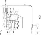
- Fig. 1 shows, in accordance with an embodiment of the present invention, a simplified schematic of a plasma processing system configured with an adjustable gap between an upper electrode assembly and a lower electrode assembly to yield a narrow gap configuration with a symmetric chamber for ultra-high pressure and/or low conductance regime.
- Plasma processing system 100 may be a single, double or triple frequency capacitively discharged system or may be an inductively coupled plasma system or a plasma system employing a different plasma generating and/or sustaining technology.
- radio frequency may include, but are not limited to, 2, 27 and 60 MHz.
- plasma processing system 100 may be configured with an upper electrode assembly 102 and a lower electrode assembly 104, in an embodiment.
- the upper electrode assembly 102 and lower electrode assembly 104 may be separated from each other by a chamber gap 106.
- the upper electrode assembly 102 may include at least an upper electrode that may be grounded or powered by an RF power supply (not shown).
- upper electrode assembly 102 may be grounded in an embodiment. Further, upper electrode assembly 102 may be configured with an inner upper electrode component 102a and an outer upper electrode component 102b in an embodiment. Outer electrode component 102b may be an annular extension of inner upper electrode 102a in an embodiment. Herein, outer electrode component 102b may be referred to as an upper electrode peripheral extension (UE-PE).
- UE-PE upper electrode peripheral extension
- inner upper electrode component 102a and UE-PE 102b may be formed from different components as shown in Fig. 1 .
- inner upper electrode 102a and UE-PE 102b may be formed as a monolithic unit in an embodiment.
- inner upper electrode 102a and/or UE-PE 102b may be formed from a plurality of components in an embodiment.
- Lower electrode assembly 104 may be configured with an electrostatic chuck (ESC) 110, an edge ring 112, an insulator ring 114, a focus ring 116, a quartz cover ring 118, confinement ring assembly 124, and/or a by-pass ring 120 in an embodiment.
- by-pass ring 120 may be formed from aluminum.
- by-pass ring 120 may be configured with a by-pass cavity 122 to allow gas to exhaust through by-pass cavity 122.
- a vat valve 134 coupled to a turbo molecular pump (TMP) 136 may be employed to exhaust processed gas from plasma processing system 100.
- TMP turbo molecular pump
- UE-PE 102b may be configured with a step, i.e., choke point 126.
- the lower surface of UE-PE 102b may extend or protrude below the lower surface of inner upper electrode 102a.
- the lower surface of UE-PE 102b and the top surface of quartz cover ring 118 may be separated by a second gap 128 in an embodiment.
- the size of gap 128 may be adjustable by moving upper electrode assembly 102 and/or lower electrode assembly in an embodiment.
- the choke point may be formed by making a non co-planar step.
- the UF-PE may extend or protrude below the surface of the upper electrode.
- a lower electrode periphery extension (LE-PE) may be employed to be non-coplanar with the lower electrode.
- the LE-PE may be raised above the electrode.
- the LE-PE may be quartz cover ring 118.
- plasma processing system 100 may be configured with two possible plasma sustaining regions: region 130a OR regions 130a plus 128 plus 130b.
- region 130a may be capable of sustaining plasma whenever chamber gap 106 is sufficiently large to sustain plasma.
- regions 130a plus 128 plus 130b may be capable of sustaining plasm whenever gap 128 in the choke region is sufficiently large to sustain plasma in an embodiment. This is depicted in Figure 2 .
- processed gas (not shown) may be supplied into chamber gap 106.
- the processed gas being supplied into chamber gap 106 may be excited into a plasma state by RF power supplied to lower electrode assembly 104.
- RF power supplied to lower electrode assembly 104 may be supplied to lower electrode assembly 104.
- plasma may be sustained in region 130a of chamber gap 106 in an embodiment.
- Gap 128 of choke region may be insufficiently large to sustain plasma. Therefore, region 130b may be incapable of sustaining plasma.
- confinement ring assembly 124 is pulled up to limit additional flow obstructions.
- the upper electrode and lower electrode may be sized such that in the narrow-gap configuration, a 1:1 area ratio may be achieved, making the chamber a symmetric chamber in the narrow-gap configuration.
- differential pressure between region 130a and the rest of plasma processing system may be attained and controlled in an embodiment.
- the pressure in chamber gap 106 may be controlled by an active feedback loop.
- the pressure in region 130a may be measures and gap 128, vat valve 134 and/or gas flow rate may be adjusted to control the pressure in region 130a.
- ultra-high pressure e.g., in the hundreds of Pa range (in the Torr range)
- Lower electrode assembly 104 may be moved to a reduced height to form a very narrow gap for gap 128.
- the choke region of gap 128 may represent an area of very high flow restriction choking the gas flow significantly.
- the height of gap 128 is insufficiently large to sustain plasma in gap 128 and/or region 130b.
- pressure in region 130a may be controlled by adjusting the height of gap 128.
- the pressure in region 130a may be increased by further reducing the height of gap 128.
- gap 128 remains insufficiently large to sustain plasma in region 130b throughout the range of pressure controlled through adjusting gap 128.
- the pressure in region 130a may be controlled by adjusting the flow of processed gas through region 130a in an embodiment
- the flow of processed gas may be increased to increase pressure in region 130a to increase pressure to attain ultra-high pressure in region 130a.
- pressure control of region 130a may be achieved by adjusting vat valve 134 upstream of TMP 136 in an embodiment.
- vat valve 134 may be throttle closed to back pressure plasma chamber region to increase pressure to attain ultra-high pressure in region 130a.
- a confinement ring set 124 may not be employed in pressure control for ultra-high pressure regime because flow restriction is insignificant in comparison to the flow restriction from gap 128.
- confinement ring set 124 is parallel of by-pass ring 120, which has even higher conductance than the gaps between confinement ring set 124.
- confinement ring set 124 may be configured in the collapsed state resting on shoulder 132 of by-pass ring 120 or may be pulled up into the wafer transport position as shown in Figure 1 . Gas conductance through by-pass cavity 122 of by-pass ring 120 may render pressure control from confinement ring set 124 inconsequential.
- region 130a may be able to attain ultra-high pressure, e.g., up to about 667 Pa (about 5 Torr), due to the high flow rate and/or the high flow restriction.
- ultra-high pressure e.g., up to about 667 Pa (about 5 Torr)
- a symmetric chamber with a narrow gap configuration may attain ultra-high pressure and/or low conductance independent of the rest of the processing chamber in an embodiment.
- gap 128 may be employed to extinguish plasma in region 130b by narrowing the size of gap 128 to be insufficient large to sustain plasma.
- gap 128 may be employed not only to extinguish plasma in region 130b, but gap 128 may be adjusted to control pressure in region 130b. Thus, gap 128 may be narrowed beyond the point to extinguish plasma for pressure control.
- FIG. 1 is employed to illustrate the example of low pressure and/or high conductance regime with the symmetric chamber.
- lower electrode assembly 104 may be moved such that gap 128 is sufficiently large to reduce flow restriction but still able to prevent plasma ignition in region 130b in an embodiment.
- Gap 128 is sufficiently narrowed to extinguish plasma, and plasma is not sustained in region 130b.
- gap 128 may be sufficiently large to increase gas conductance resulting in lower pressure in region 130a.
- pressure control of region 130a may be attained by adjusting gap 128.
- the upper range for the seize of gap 128 may be limited to the size of gap 128 (relative to the mean free path) to sustain plasma in an embodiment.
- the pressure in region 130a may be controlled by adjusting the flow of processed gas through region 130a in an embodiment.
- the flow of processed gas may be reduced to decrease pressure in region 130a.
- pressure control of region 130a may be achieved by adjusting vat valve 134 upstream of TMP 136 in an embodiment.
- vat valve 134 may be throttle opened to reduce pressure in region 130a.
- confinement ring set 124 may be employed to control pressure. Referring to Fig. 1 , confinement ring set 124 may be lowered and pressure in region 130a may be controlled by adjusting the gaps between confinement ring set 124. Methods for controlling pressure employing confinement ring set is well known by those skilled in the art and is not discussed in detail to simplify discussion.
- a lower pressure regime may be achieved with symmetric chamber configuration by adjusting gap 128 to increase conductance while preventing external region 130b from sustaining plasma.
- Pressure in region 130a may be controlled by adjusting gap 128, confinement ring set 124, gas flow rate, and/or vat valve 134.
- Fig. 2 shows, in accordance with an embodiment of the present invention, a simplified schematic of a plasma processing system configured with an adjustable gap between an upper electrode assembly 102 and a lower electrode assembly 104 to yield a wide gap configuration with an asymmetric chamber for low pressure and/or high conductance regime.
- Fig. 2 is discussed in relation to Fig. 1 to facilitate understanding.
- low pressure e.g., as low as about 0.67 Pa (about 5 milli-Torr)
- the low pressure and/or high conductance may be attained by moving lower electrode assembly 104 in the direction of an arrow 240 to increase the height of gap 128 in an embodiment.
- the increase in height of gap 128 may result in higher conductance.
- gap 128 is sufficiently large and plasma may be sustained in a region 230. Region 230 may extend from the center of the chamber out to the inner edge of confinement ring sent 124.
- confinement ring set 124 may be employed to confine plasma within a specific region.
- the area ratio of the grounded upper electrode to the powered lower electrode may be high, i.e., the ratio may be greater than 1:1, making the chamber asymmetric.
- plasma is sustained in region 230 for the asymmetric configuration as shown in Fig. 2 instead of plasma being only sustained in region 130a as shown in Fig. 1 .
- a high ratio of ground to powered RF electrode areas may result in high bias voltage and high ion energy at substrate 108 for the wide-gap configuration.
- gas may flow out of region 230 through by-pass cavity 122 of by-pass ring 120 contributing to the capability of attaining low pressure for the asymmetric configuration. Due to by-pass cavity 122 and the increased height of gap 128, the high pressure that may be attained in the asymmetric configuration may be limited.
- pressure in region 230 may be controlled by adjusting the gaps of confinement ring set 124, as shown in Fig. 2 .
- Confinement ring set 124 may be lowered and pressure may be controlled by adjusting the gaps between confinement ring set 124.
- the pressure in region 230 may be controlled by adjusting the flow of processed gas through region 130 in an embodiment
- the flow of processed gas may be reduced to decrease pressure in region 230.
- pressure control of region 230 may be achieved by adjusting vat valve 134 upstream of TMP 136 in an embodiment.
- vat valve 134 may be throttle opened to reduce pressure in region 230.
- a lower pressure regime with increased conductance may be achieved in a wide-gap configuration of gap128 with an asymmetric chamber.
- Pressure in region 230 may be controlled by adjusting gaps between the confinement ring set 124, gas flow rate, and/or vat valve 134.
- embodiments of the invention permit differentiated pressure control to provide a wide range of pressure and/or conductance in a plasma processing system.
- the range of pressure that may be attained may be from about 0.67 Pa to about 667 Pa (from about 5 milli-Torr to about 5 Torr).
- plasma processing in the gamma mode may be possible.
- the different gap configurations may allow for control of grounded upper electrode to powered lower electrode area ratio allowing control of wafer bias and ion energy as well as ion energy distribution.
- substrate requiring various recipes over a wide range of pressure and/or bias and ion energy or ion energy distribution may be performed using the same plasma processing chamber reducing cost and/or time delay that may incur in employing multiple plasma processing chambers.
Landscapes
- Engineering & Computer Science (AREA)
- Physics & Mathematics (AREA)
- Plasma & Fusion (AREA)
- Chemical & Material Sciences (AREA)
- Analytical Chemistry (AREA)
- General Physics & Mathematics (AREA)
- Condensed Matter Physics & Semiconductors (AREA)
- Manufacturing & Machinery (AREA)
- Computer Hardware Design (AREA)
- Microelectronics & Electronic Packaging (AREA)
- Power Engineering (AREA)
- Plasma Technology (AREA)
- Drying Of Semiconductors (AREA)
- Chemical Vapour Deposition (AREA)
Description
- Advances in plasma processing have facilitated growth in the semiconductor industry. The semiconductor industry is a highly competitive market. The ability for a manufacturing company to be able to process substrates in different processing conditions may give the manufacturing company an edge over competitors. Thus, manufacturing companies have dedicated time and resources to identify methods and/or arrangements for improving substrate processing.
- A typical processing system that may be employed to perform substrate processing may be a capacitively-coupled plasma (CCP) processing system. The plasma processing system may be built to enable processing in a range of process parameters. However, in recent years, the types of devices that may be processed have become more sophisticated and may require more precise process control. For example, devices being processed are becoming smaller with finer features and may require more precise control of plasma parameters, such as plasma density and uniformity across the substrate, for better yield. Pressure control of the wafer area in the etching chamber may be an example of a process parameter affecting plasma density and uniformity.
- The manufacturing of semiconductor devices may require multi-step processes employing plasma within a plasma processing chamber. During plasma processing of semiconductor device(s), the plasma processing chamber may typically be maintained at a predefined pressure for each step of the process. The redefined pressure may be achieved through employing mechanical vacuum pump(s), turbo pump(s), confinement ring positioning and/or combinations thereof, as is well known by those skilled in the art.
- Conventionally, a valve assembly may be employed to throttle the exhaust turbo pump(s) to attain pressure control for maintaining predefined pressure conditions in the plasma processing chamber. However, the pressure being controlled by the vat valve may result in a global change in the entire chamber without the capability of providing differential pressure control in different regions of the chamber.
- In the prior art, the pressure in the plasma generating region of the plasma processing chamber (e.g., the region encapsulated by the two electrodes and surrounded by the confinement rings) may be controlled by adjusting the gaps between the confinement rings of a confinement ring assembly. Adjusting the gaps controls the flow rate of exhaust gas from the plasma generating region and pressure may be affected as a result. The overall gas flow conductance out of the plasma generating region may depend on several factors, including but not limited to, the number of confinement rings and the size of the gaps between the confinement rings. Thus, the operating windows for the pressure range may be limited by the chamber gap and/or the gaps of these confinement rings. Furthermore, the plasma cross section may be a fixed diameter for the aforementioned process due to the fix diameter of these confinement rings.
- In the prior art, a plasma processing chamber configured with the capability to sustain a plurality of differentiated plasma volumes may be employed to address the aforementioned problem of plasma of fixed cross section. In an example, a wide-gap configuration may be employed to provide an increased plasma cross section with relatively low pressure. In another example, a narrow-gap configuration may be employed to provide the conventional plasma cross section but relatively higher pressure may be attained. However, active differentiated pressure control for the system is not provided. Document
WO-A2-02/31859 - Document
JP 2004119448 - Document
US-A1-0040931 discloses a parallel-plate plasma processing system comprising a focus ring arranged on the lower electrode and a shield ring mounted on the top electrode. DocumentUS-A1-20080241420 discloses a plasma processing system including an upper electrode with a stepped peripheral extension, and a lower electrode with a cover ring. DocumentWO-A2-2008/082518 discloses a capacitively-coupled plasma chamber, wherein the plasma conditions can be quickly and accurately controlled by a confinement ring assembly, which enables pressure control and plasma confinement over the entire range of the interelectrode gap, and a by-pass ring. - In view of the need to process the substrate in multiple steps, each of which may involve a different pressure, improvement to the capability to provide differentiated pressure control over a wider range of pressure in plasma processing systems is highly desirable.
- The invention relates, in an embodiment, to a plasma processing system having a plasma processing chamber configured for processing a substrate. The plasma processing system includes at least an upper electrode and a lower electrode for processing the substrate. The substrate is disposed on the lower electrode during plasma processing, where the upper electrode and the substrate forms a first gap. The plasma processing system also includes an upper electrode peripheral extension (UE-PE). The UE-PE is mechanically coupled to a periphery of the upper electrode, where the UE-PE is configured to be non-coplanar with the upper electrode. The plasma processing system further includes a cover ring. The cover ring is configured to concentrically surround the lower electrode, where the UE-PE and the cover ring forms a second gap.
- The above summary relates to only one of the many embodiments of the invention disclosed herein and is not intended to limit the scope of the invention, which is set forth is the claims herein. These and other features of the present invention will be described in more detail below in the detailed description of the invention and in conjunction with the following figures.
- The present invention is illustrated by way of example, and not by way of limitation, in the figures of the accompanying drawings and in which like reference numerals refer to similar elements and in which:
-
Fig. 1 shows, in accordance with an embodiment of the present invention, a simplified schematic of a plasma processing system configured with an adjustable gap between an upper electrode assembly and a lower electrode assembly to yield a narrow gap configuration with a symmetric chamber for ultra-high pressure and/or low conductance regime. -
Fig. 2 shows, in accordance with an embodiment of the present invention, a simplified schematic of a plasma processing system configured with an adjustable gap between an upper electrode assembly and a lower electrode assembly to yield a wide gap configuration with an asymmetric chamber for low pressure and/or high conductance regime. - The present invention will now be described in detail with reference to a few embodiments thereof as illustrated in the accompanying drawings. In the following description, numerous specific details are set forth in order to provide a thorough understanding of the present invention. It will be apparent however, to one skilled in the art, that the present invention may be practiced without some or all of these specific details. In other instances, well known process steps and/or structures have not been described in detail in order to not unnecessarily obscure the present invention.
- In accordance with embodiments of the invention, there are provided methods and apparatus for providing a wide range of pressure in the same plasma processing chamber. In some plasma processing systems, the chamber gap (i.e., the gap between the upper and lower electrode) is a recipe parameter and may vary from step to step. In these plasma processing systems, there may be provided a mechanism configured to move the lower electrode assembly to adjust the chamber gap. In other plasma processing systems, the upper electrode assembly may be moved. In the disclosure herein, the chamber is assumed to have a moving lower electrode. It should be understood, however, that embodiments of the invention herein apply equally well to chambers in which the upper electrode is movable (alternatively or additionally).
- In one ore more embodiments, the upper electrode is grounded while the lower electrode is powered. In an implementation, the periphery of the upper electrode is provided with an annular, i.e., donut-shaped, ring that surrounds the upper electrode. The annular extension is referred herein as the upper electrode peripheral extension (UE-PE).
- The gap bellow the UE-PE is to a quartz cover ring may be configured such that as the gap between the upper electrode and the lower electrode is sufficiently narrowed, there comes a point where the gap below the UE-PE is insufficiently large to sustain plasma below the UE-PE while the gap that under lies the upper electrode inside of the UE-PE still remain sufficiently large to sustain plasma. In this narrow-gap case, the gap below UE-PE may represent an area of very high flow restriction. In an embodiment, the height of the gap below UE-PE may be adjusted to control the pressure to attain ultra-high pressure and low conductance in the area of the gap that under lies the upper electrode inside of the UE-PE.
- As the gap between the upper electrode and the lower electrode is gradually enlarged whereas the gap below the UE-PE is insufficiently large to sustain plasma while the gap that under lies the upper electrode inside of the UE-PE still remain sufficiently large to sustain plasma, lower pressure and higher conductance may be achieved for the narrow-gap configuration in an embodiment.
- As the gap between the upper electrode and the lower electrode is further gradually enlarged, there comes a point where the gap below the UE-PE is sufficiently large to sustain plasma while the gap that under lies the upper electrode inside of the UE-PE is also sufficiently large to sustain plasma. In this wide-gap configuration, low pressure and high conductance may be achieved. The confinement rings may be employed to contain plasma and/or control pressure.
- As may be appreciated from the foregoing, the effective RF coupling area of the powered lower electrode remains the same for both the narrow-gap configuration and the wide-gap configuration. However, in the wide-gap configuration, the effective RF coupling area of the grounded electrode is enlarged. Accordingly, the narrow-gap configuration may provide for a first area ratio of RF coupling while the wide-gap configuration may provide for a second area ratio of RF coupling, i.e., larger due to a larger effective RF ground coupling area.
- In an embodiment, the difference in gaps (i.e., the gap between the upper electrode and lower electrode at the central region of the upper electrode and the gap below the UE-PE) may be accomplished by making the UE-PE non co-planar with the upper electrode. For example, the UE-PE may protrude below the upper electrode. The UE-PE moves together with the upper electrode in implementation wherein the upper electrode is movable.
- In another embodiment, a lower electrode periphery extension (LE-PE) may be employed to be non-coplanar with the lower electrode. For example, the LE-PE may be raised above the electrode. In an example, the LE-PE may be quartz cover ring. The LE-PE moves together with the lower electrode in implementation wherein the lower electrode is movable.
- The features and advantages of the present invention may be better understood with reference to the figures and discussions (with prior art mechanisms and embodiments of the invention contrasted) that follow.
-
Fig. 1 shows, in accordance with an embodiment of the present invention, a simplified schematic of a plasma processing system configured with an adjustable gap between an upper electrode assembly and a lower electrode assembly to yield a narrow gap configuration with a symmetric chamber for ultra-high pressure and/or low conductance regime.Plasma processing system 100 may be a single, double or triple frequency capacitively discharged system or may be an inductively coupled plasma system or a plasma system employing a different plasma generating and/or sustaining technology. In the example ofFig. 1 , radio frequency may include, but are not limited to, 2, 27 and 60 MHz. - Referring to
Fig. 1 ,plasma processing system 100 may be configured with anupper electrode assembly 102 and alower electrode assembly 104, in an embodiment. Theupper electrode assembly 102 andlower electrode assembly 104 may be separated from each other by achamber gap 106. Theupper electrode assembly 102 may include at least an upper electrode that may be grounded or powered by an RF power supply (not shown). - In the example of
Fig. 1 ,upper electrode assembly 102 may be grounded in an embodiment. Further,upper electrode assembly 102 may be configured with an innerupper electrode component 102a and an outerupper electrode component 102b in an embodiment.Outer electrode component 102b may be an annular extension of innerupper electrode 102a in an embodiment. Herein,outer electrode component 102b may be referred to as an upper electrode peripheral extension (UE-PE). - As shown in
Fig. 1 , innerupper electrode component 102a and UE-PE 102b may be formed from different components as shown inFig. 1 . Alternatively, innerupper electrode 102a and UE-PE 102b may be formed as a monolithic unit in an embodiment. Further, innerupper electrode 102a and/or UE-PE 102b may be formed from a plurality of components in an embodiment. -
Lower electrode assembly 104 may be configured with an electrostatic chuck (ESC) 110, anedge ring 112, aninsulator ring 114, afocus ring 116, aquartz cover ring 118,confinement ring assembly 124, and/or a by-pass ring 120 in an embodiment. As shown inFig. 1 , by-pass ring 120 may be formed from aluminum. In an embodiment, by-pass ring 120 may be configured with a by-pass cavity 122 to allow gas to exhaust through by-pass cavity 122. As shown inFig. 1 , avat valve 134 coupled to a turbo molecular pump (TMP) 136 may be employed to exhaust processed gas fromplasma processing system 100. The features of the aforementioned components are well known by those skilled in the art and will not be discussed in detail to simplify the discussion. - In an embodiment, UE-
PE 102b may be configured with a step, i.e.,choke point 126. As a result of the step, the lower surface of UE-PE 102b may extend or protrude below the lower surface of innerupper electrode 102a. As shown inFig. 1 , the lower surface of UE-PE 102b and the top surface ofquartz cover ring 118 may be separated by asecond gap 128 in an embodiment. The size ofgap 128 may be adjustable by movingupper electrode assembly 102 and/or lower electrode assembly in an embodiment. - In an embodiment, the choke point may be formed by making a non co-planar step. For example, the UF-PE may extend or protrude below the surface of the upper electrode. Alternatively or additionally, a lower electrode periphery extension (LE-PE) may be employed to be non-coplanar with the lower electrode. For example, the LE-PE may be raised above the electrode. In an example, the LE-PE may be
quartz cover ring 118. - As shown in
Fig. 1 ,plasma processing system 100 may be configured with two possible plasma sustaining regions:region 130a ORregions 130a plus 128 plus 130b. In an embodiment,region 130a may be capable of sustaining plasma wheneverchamber gap 106 is sufficiently large to sustain plasma. Whereas,regions 130a plus 128 plus 130b may be capable of sustaining plasm whenevergap 128 in the choke region is sufficiently large to sustain plasma in an embodiment. This is depicted inFigure 2 . - During plasma processing, processed gas (not shown) may be supplied into
chamber gap 106. The processed gas being supplied intochamber gap 106 may be excited into a plasma state by RF power supplied tolower electrode assembly 104. Consider the situation wherein, for example,slower electrode assembly 104 may be moved to create a narrow-gap configuration wherein the size ofgap 128 may be insufficient large (relative to the mean free path) to sustain plasma. - In the narrow-gap configuration of
Fig. 1 , plasma may be sustained inregion 130a ofchamber gap 106 in an embodiment.Gap 128 of choke region may be insufficiently large to sustain plasma. Therefore,region 130b may be incapable of sustaining plasma. In the narrow gap configurationconfinement ring assembly 124 is pulled up to limit additional flow obstructions. - In an embodiment, the upper electrode and lower electrode may be sized such that in the narrow-gap configuration, a 1:1 area ratio may be achieved, making the chamber a symmetric chamber in the narrow-gap configuration.
- In the narrow-gap configuration, differential pressure between
region 130a and the rest of plasma processing system may be attained and controlled in an embodiment. In an example, the pressure inchamber gap 106 may be controlled by an active feedback loop. In an embodiment, the pressure inregion 130a may be measures andgap 128,vat valve 134 and/or gas flow rate may be adjusted to control the pressure inregion 130a. - Consider the situation wherein, for example, ultra-high pressure, e.g., in the hundreds of Pa range (in the Torr range), may be desired in
region 130a during plasma processing of asubstrate 108.Lower electrode assembly 104 may be moved to a reduced height to form a very narrow gap forgap 128. The choke region ofgap 128 may represent an area of very high flow restriction choking the gas flow significantly. In an embodiment, the height ofgap 128 is insufficiently large to sustain plasma ingap 128 and/orregion 130b. - Through the aforementioned active pressure feedback loop, pressure in
region 130a may be controlled by adjusting the height ofgap 128. For example, the pressure inregion 130a may be increased by further reducing the height ofgap 128. In anembodiment gap 128 remains insufficiently large to sustain plasma inregion 130b throughout the range of pressure controlled throughadjusting gap 128. - Alternatively and/or additionally, the pressure in
region 130a may be controlled by adjusting the flow of processed gas throughregion 130a in an embodiment In an example, the flow of processed gas may be increased to increase pressure inregion 130a to increase pressure to attain ultra-high pressure inregion 130a. - Alternatively and/or additionally, pressure control of
region 130a may be achieved by adjustingvat valve 134 upstream ofTMP 136 in an embodiment. In an example,vat valve 134 may be throttle closed to back pressure plasma chamber region to increase pressure to attain ultra-high pressure inregion 130a. - Referring to
Fig. 1 , a confinement ring set 124 may not be employed in pressure control for ultra-high pressure regime because flow restriction is insignificant in comparison to the flow restriction fromgap 128. In addition, confinement ring set 124 is parallel of by-pass ring 120, which has even higher conductance than the gaps between confinement ring set 124. For example, confinement ring set 124 may be configured in the collapsed state resting onshoulder 132 of by-pass ring 120 or may be pulled up into the wafer transport position as shown inFigure 1 . Gas conductance through by-pass cavity 122 of by-pass ring 120 may render pressure control from confinement ring set 124 inconsequential. - Accordingly,
region 130a may be able to attain ultra-high pressure, e.g., up to about 667 Pa (about 5 Torr), due to the high flow rate and/or the high flow restriction. Thus, a symmetric chamber with a narrow gap configuration may attain ultra-high pressure and/or low conductance independent of the rest of the processing chamber in an embodiment. - In the prior art,
gap 128 may be employed to extinguish plasma inregion 130b by narrowing the size ofgap 128 to be insufficient large to sustain plasma. In contrast,gap 128 may be employed not only to extinguish plasma inregion 130b, butgap 128 may be adjusted to control pressure inregion 130b. Thus,gap 128 may be narrowed beyond the point to extinguish plasma for pressure control. - Consider another situation wherein, for example, low pressure and/or high conductance may be desired in
region 130a during plasma processing for the configuration with a symmetric chamber and narrow gap.Fig. 1 is employed to illustrate the example of low pressure and/or high conductance regime with the symmetric chamber. For example,lower electrode assembly 104 may be moved such thatgap 128 is sufficiently large to reduce flow restriction but still able to prevent plasma ignition inregion 130b in an embodiment. - Referring to
Fig. 1 , plasma is sustained inregion 130a.Gap 128 is sufficiently narrowed to extinguish plasma, and plasma is not sustained inregion 130b. In an embodiment,gap 128 may be sufficiently large to increase gas conductance resulting in lower pressure inregion 130a. In an embodiment, pressure control ofregion 130a may be attained by adjustinggap 128. The upper range for the seize ofgap 128 may be limited to the size of gap 128 (relative to the mean free path) to sustain plasma in an embodiment. - Alternatively and/or additionally, the pressure in
region 130a may be controlled by adjusting the flow of processed gas throughregion 130a in an embodiment. In an example, the flow of processed gas may be reduced to decrease pressure inregion 130a. - Alternatively and/or additionally, pressure control of
region 130a may be achieved by adjustingvat valve 134 upstream ofTMP 136 in an embodiment. In an example,vat valve 134 may be throttle opened to reduce pressure inregion 130a. - In the low pressure regime with the symmetric chamber, confinement ring set 124 may be employed to control pressure. Referring to
Fig. 1 , confinement ring set 124 may be lowered and pressure inregion 130a may be controlled by adjusting the gaps between confinement ring set 124. Methods for controlling pressure employing confinement ring set is well known by those skilled in the art and is not discussed in detail to simplify discussion. - Accordingly, a lower pressure regime may be achieved with symmetric chamber configuration by adjusting
gap 128 to increase conductance while preventingexternal region 130b from sustaining plasma. Pressure inregion 130a may be controlled by adjustinggap 128, confinement ring set 124, gas flow rate, and/orvat valve 134. -
Fig. 2 shows, in accordance with an embodiment of the present invention, a simplified schematic of a plasma processing system configured with an adjustable gap between anupper electrode assembly 102 and alower electrode assembly 104 to yield a wide gap configuration with an asymmetric chamber for low pressure and/or high conductance regime.Fig. 2 is discussed in relation toFig. 1 to facilitate understanding. - Consider the situation wherein, for example, low pressure, e.g., as low as about 0.67 Pa (about 5 milli-Torr), may be desired for processing of
substrate 108 inplasma processing system 200, as shown inFig. 2 . The low pressure and/or high conductance may be attained by movinglower electrode assembly 104 in the direction of anarrow 240 to increase the height ofgap 128 in an embodiment. The increase in height ofgap 128 may result in higher conductance. In an embodiment,gap 128 is sufficiently large and plasma may be sustained in aregion 230.Region 230 may extend from the center of the chamber out to the inner edge of confinement ring sent 124. As shown inFig. 2 . confinement ring set 124 may be employed to confine plasma within a specific region. - In the wide-gap configuration of
Fig. 2 , the area ratio of the grounded upper electrode to the powered lower electrode may be high, i.e., the ratio may be greater than 1:1, making the chamber asymmetric. In contrast to the symmetric configuration, plasma is sustained inregion 230 for the asymmetric configuration as shown inFig. 2 instead of plasma being only sustained inregion 130a as shown inFig. 1 . For example, a high ratio of ground to powered RF electrode areas may result in high bias voltage and high ion energy atsubstrate 108 for the wide-gap configuration. - As shown in
Fig. 2 , gas may flow out ofregion 230 through by-pass cavity 122 of by-pass ring 120 contributing to the capability of attaining low pressure for the asymmetric configuration. Due to by-pass cavity 122 and the increased height ofgap 128, the high pressure that may be attained in the asymmetric configuration may be limited. - In the low pressure asymmetric configuration, pressure in
region 230 may be controlled by adjusting the gaps of confinement ring set 124, as shown inFig. 2 . Confinement ring set 124 may be lowered and pressure may be controlled by adjusting the gaps between confinement ring set 124. - Alternatively and/or additionally, the pressure in
region 230 may be controlled by adjusting the flow of processed gas through region 130 in an embodiment In an example, the flow of processed gas may be reduced to decrease pressure inregion 230. - Alternatively and/or additionally, pressure control of
region 230 may be achieved by adjustingvat valve 134 upstream ofTMP 136 in an embodiment. In an example,vat valve 134 may be throttle opened to reduce pressure inregion 230. - Accordingly, a lower pressure regime with increased conductance may be achieved in a wide-gap configuration of gap128 with an asymmetric chamber. Pressure in
region 230 may be controlled by adjusting gaps between the confinement ring set 124, gas flow rate, and/orvat valve 134. - As can be appreciated from the forgoing, embodiments of the invention permit differentiated pressure control to provide a wide range of pressure and/or conductance in a plasma processing system. The range of pressure that may be attained may be from about 0.67 Pa to about 667 Pa (from about 5 milli-Torr to about 5 Torr). In the ultra-higb pressure range, plasma processing in the gamma mode may be possible. Furthermore, the different gap configurations may allow for control of grounded upper electrode to powered lower electrode area ratio allowing control of wafer bias and ion energy as well as ion energy distribution. Thus, substrate requiring various recipes over a wide range of pressure and/or bias and ion energy or ion energy distribution may be performed using the same plasma processing chamber reducing cost and/or time delay that may incur in employing multiple plasma processing chambers.
- While this invention has been described in terms of several embodiments, there are alterations, permutations, and equivalents, which fall within the scope of this invention. It should also be noted that there are many alternative ways of implementing the methods and apparatuses of the present invention. Furthermore, embodiments of the present invention may find utility in other applications. The abstract section is provided herein for convenience and, due to word count limitation, is accordingly written for reading convenience and should not be employed to limit the scope of the invention. It is therefore intended that the invention be interpreted as including all such alterations, permutations, and equivalents as fall within the scope of the present invention. The invention is defined by the claims.
Claims (13)
- A plasma processing system having a plasma processing chamber configured to process a substrate (108), comprising:an upper electrode assembly (102) and a lower electrode assembly (104) for processing said substrate (108), the upper electrode assembly (102) comprising an upper electrode (102a) and an upper electrode peripheral extension (102b), the lower electrode assembly (104) comprising a lower electrode (110) and a cover ring (118), said substrate (108) being disposed on said lower electrode (110) during plasma processing, wherein said upper electrode (102a) and said lower electrode are arranged to form a first gap (106), wherein said upper electrode (102a) is arranged such that, in use, it is grounded and wherein said lower electrode (110) is arranged such that, in use, it is powered;wherein said upper electrode peripheral extension (102b) is arranged to be mechanically coupled to a periphery of said upper electrode (102a), wherein said upper electrode peripheral extension (102b) is configured to be non-coplanar with said upper electrode (102a), wherein said upper electrode peripheral extension (102b) is arranged such that, in use, it is grounded,wherein said cover ring (118) is configured to concentrically surround said lower electrode (110), where said upper electrode peripheral extension and said cover ring are arranged to form a second gap (128),wherein said second gap (128) is smaller than said first gap (106), the plasma processing system further comprising a mechanism configured to move one of said upper electrode assembly (102) and said lower electrode assembly (104) in a direction perpendicular to a planar surface of said lower electrode (110) so as to simultaneously adjust said second gap (128) and said first gap (106) and so as to permit differentiated pressure control to provide a wide range of pressure and/or gas conductance in the plasma processing system.
- The plasma processing system of claim 1, wherein said upper electrode peripheral extension (102b) and said upper electrode (102a) are formed as a monolithic unit.
- The plasma processing system of claim 1, wherein said upper electrode peripheral extension (102b) and said upper electrode (102a) are formed from a plurality of components.
- The plasma processing system of claim 1 further comprising a by-pass ring assembly.
- The plasma processing system of claim 1 further comprising a confinement ring assembly (124).
- The plasma processing system of claim 1 wherein said cover ring (118) is at least partially covered with quartz.
- The plasma processing system of claim 1 further comprising a by-pass ring (120) having a by-pass cavity (122) for evacuating at least a portion of exhaust gas produced by said processing.
- A method for controlling pressure in a plasma processing chamber, said method comprising:providing at least an upper electrode (102a) and a lower electrode (110) for processing a substrate (108), disposing said substrate (108) on said lower electrode (110) during plasma processing, forming a first gap (106) between said upper electrode (102a) and said lower electrode (110), grounding said upper electrode (102a) and powering said lower electrode (110);providing an upper electrode peripheral extension (102b), mechanically coupling said upper electrode peripheral extension (102b) to a periphery of said upper electrode, configuring said upper electrode peripheral extension (102b) to be non-coplanar with said upper electrode, grounding said upper electrode peripheral extension ;providing a cover ring (118) configured to concentrically surround said lower electrode (110), forming a second gap (128) between said upper electrode peripheral extension (102b) and said cover ring (118), wherein said second gap (128) is smaller than said first gap (106);generating a plasma within said plasma processing chamber to process said substrate; andsimultaneously adjusting said second gap and said first gap to permit differentiated pressure control to provide a wide range of pressure and/or gas conductance in the plasma processing system.
- The method of claim 8, wherein said adjusting further include moving one of said upper electrode (102a) and said lower electrode (110) in a direction perpendicular to a planar surface of said lower electrode to change the height of said second gap (128), or
wherein said upper electrode peripheral extension (102b) and said upper electrode (102a) are formed as a monolithic unit, or
wherein said upper electrode peripheral extension (102b) and said upper electrode are formed from a plurality of components. - The method of claim 8 wherein said plasma processing chamber further includes a set of confinement rings, said method including:deploying said set of confinement rings to regulate a process pressure when a first gap (106) exists between said upper electrode (102a) and said lower electrode (110); andcompletely stowing said set of confinement rings when a second gap (128) exists between said upper electrode and said lower electrode due to said simultaneously adjusting, wherein said first gap is larger than said second gap.
- The method of claim 8 wherein said cover ring (118) is at least partially covered with quartz.
- A method for changing an area ratio of the upper electrode to the lower electrode in a plasma processing chamber, said method comprising:providing at least an upper electrode (102a) and a lower electrode (110) for processing a substrate (108), disposing said substrate (108) on said lower electrode (110) during plasma processing, forming a first gap (106) between said upper electrode (102a) and said lower electrode (110), grounding said upper electrode (102a) and powering said lower electrode (110); providing an upper electrode peripheral extension (102b), mechanically coupling said upper electrode peripheral extension to a periphery of said upper electrode, configuring said upper electrode peripheral extension to be non-coplanar with said upper electrode, grounding said upper electrode peripheral extension (102b);providing a cover ring (118) configured to concentrically surround said lower electrode, forming a second gap (128) between said upper electrode peripheral extension (102b) and said cover ring (118), wherein said second gap (128) is smaller than said first gap (106);generating a plasma within said plasma processing chamber to process said substrate; andsimultaneously adjusting said second gap and said first gap to change said area ratio of the upper electrode (102a) to the lower electrode (110) within said plasma processing chamber, said adjusting including moving one of said upper electrode and said lower electrode in a direction perpendicular to a planar surface of said lower electrode.
- The method of claim 12 wherein only said upper electrode (102a) of said upper electrode (102a) and said lower electrode (110) is adjustable, or
wherein only said lower electrode (110) of said upper electrode (102a) and said lower electrode (110) is adjustable, or
wherein said adjusting results in at least a first area ratio and a second area ratio, said first area ratio representing 1:1 and thereby emulating a symmetric plasma processing chamber, said second area ratio is other than 1:1 and thereby emulating a non-symmetric plasma processing chamber.
Applications Claiming Priority (3)
| Application Number | Priority Date | Filing Date | Title |
|---|---|---|---|
| US13948108P | 2008-12-19 | 2008-12-19 | |
| US12/368,843 US8869741B2 (en) | 2008-12-19 | 2009-02-10 | Methods and apparatus for dual confinement and ultra-high pressure in an adjustable gap plasma chamber |
| PCT/US2009/068183 WO2010080420A2 (en) | 2008-12-19 | 2009-12-16 | Methods and apparatus for dual confinement and ultra-high pressure in an adjustable gap plasma chamber |
Publications (3)
| Publication Number | Publication Date |
|---|---|
| EP2380412A2 EP2380412A2 (en) | 2011-10-26 |
| EP2380412A4 EP2380412A4 (en) | 2015-03-18 |
| EP2380412B1 true EP2380412B1 (en) | 2017-09-27 |
Family
ID=42266749
Family Applications (1)
| Application Number | Title | Priority Date | Filing Date |
|---|---|---|---|
| EP09837887.0A Active EP2380412B1 (en) | 2008-12-19 | 2009-12-16 | Methods and apparatus for dual confinement and ultra-high pressure in an adjustable gap plasma chamber |
Country Status (8)
| Country | Link |
|---|---|
| US (2) | US8869741B2 (en) |
| EP (1) | EP2380412B1 (en) |
| JP (1) | JP5872291B2 (en) |
| KR (1) | KR101591128B1 (en) |
| CN (1) | CN102257885B (en) |
| SG (1) | SG10201705046SA (en) |
| TW (2) | TWI593317B (en) |
| WO (1) | WO2010080420A2 (en) |
Families Citing this family (83)
| Publication number | Priority date | Publication date | Assignee | Title |
|---|---|---|---|---|
| US8869741B2 (en) * | 2008-12-19 | 2014-10-28 | Lam Research Corporation | Methods and apparatus for dual confinement and ultra-high pressure in an adjustable gap plasma chamber |
| US10283321B2 (en) | 2011-01-18 | 2019-05-07 | Applied Materials, Inc. | Semiconductor processing system and methods using capacitively coupled plasma |
| US9224618B2 (en) * | 2012-01-17 | 2015-12-29 | Lam Research Corporation | Method to increase mask selectivity in ultra-high aspect ratio etches |
| JP5970268B2 (en) * | 2012-07-06 | 2016-08-17 | 株式会社日立ハイテクノロジーズ | Plasma processing apparatus and processing method |
| US9132436B2 (en) | 2012-09-21 | 2015-09-15 | Applied Materials, Inc. | Chemical control features in wafer process equipment |
| US10256079B2 (en) | 2013-02-08 | 2019-04-09 | Applied Materials, Inc. | Semiconductor processing systems having multiple plasma configurations |
| US9362130B2 (en) | 2013-03-01 | 2016-06-07 | Applied Materials, Inc. | Enhanced etching processes using remote plasma sources |
| US9309598B2 (en) | 2014-05-28 | 2016-04-12 | Applied Materials, Inc. | Oxide and metal removal |
| US9966240B2 (en) | 2014-10-14 | 2018-05-08 | Applied Materials, Inc. | Systems and methods for internal surface conditioning assessment in plasma processing equipment |
| US9355922B2 (en) | 2014-10-14 | 2016-05-31 | Applied Materials, Inc. | Systems and methods for internal surface conditioning in plasma processing equipment |
| US11637002B2 (en) | 2014-11-26 | 2023-04-25 | Applied Materials, Inc. | Methods and systems to enhance process uniformity |
| US10224210B2 (en) | 2014-12-09 | 2019-03-05 | Applied Materials, Inc. | Plasma processing system with direct outlet toroidal plasma source |
| US10573496B2 (en) | 2014-12-09 | 2020-02-25 | Applied Materials, Inc. | Direct outlet toroidal plasma source |
| US11257693B2 (en) | 2015-01-09 | 2022-02-22 | Applied Materials, Inc. | Methods and systems to improve pedestal temperature control |
| US9728437B2 (en) | 2015-02-03 | 2017-08-08 | Applied Materials, Inc. | High temperature chuck for plasma processing systems |
| US20160225652A1 (en) | 2015-02-03 | 2016-08-04 | Applied Materials, Inc. | Low temperature chuck for plasma processing systems |
| US9691645B2 (en) | 2015-08-06 | 2017-06-27 | Applied Materials, Inc. | Bolted wafer chuck thermal management systems and methods for wafer processing systems |
| US9741593B2 (en) | 2015-08-06 | 2017-08-22 | Applied Materials, Inc. | Thermal management systems and methods for wafer processing systems |
| US9349605B1 (en) | 2015-08-07 | 2016-05-24 | Applied Materials, Inc. | Oxide etch selectivity systems and methods |
| US10504700B2 (en) | 2015-08-27 | 2019-12-10 | Applied Materials, Inc. | Plasma etching systems and methods with secondary plasma injection |
| US10533251B2 (en) | 2015-12-31 | 2020-01-14 | Lam Research Corporation | Actuator to dynamically adjust showerhead tilt in a semiconductor processing apparatus |
| US9953843B2 (en) * | 2016-02-05 | 2018-04-24 | Lam Research Corporation | Chamber for patterning non-volatile metals |
| US10504754B2 (en) | 2016-05-19 | 2019-12-10 | Applied Materials, Inc. | Systems and methods for improved semiconductor etching and component protection |
| US10522371B2 (en) | 2016-05-19 | 2019-12-31 | Applied Materials, Inc. | Systems and methods for improved semiconductor etching and component protection |
| US9865484B1 (en) | 2016-06-29 | 2018-01-09 | Applied Materials, Inc. | Selective etch using material modification and RF pulsing |
| US10629473B2 (en) | 2016-09-09 | 2020-04-21 | Applied Materials, Inc. | Footing removal for nitride spacer |
| US10546729B2 (en) | 2016-10-04 | 2020-01-28 | Applied Materials, Inc. | Dual-channel showerhead with improved profile |
| US9934942B1 (en) | 2016-10-04 | 2018-04-03 | Applied Materials, Inc. | Chamber with flow-through source |
| US10062579B2 (en) | 2016-10-07 | 2018-08-28 | Applied Materials, Inc. | Selective SiN lateral recess |
| US9768034B1 (en) | 2016-11-11 | 2017-09-19 | Applied Materials, Inc. | Removal methods for high aspect ratio structures |
| US10163696B2 (en) | 2016-11-11 | 2018-12-25 | Applied Materials, Inc. | Selective cobalt removal for bottom up gapfill |
| US10242908B2 (en) | 2016-11-14 | 2019-03-26 | Applied Materials, Inc. | Airgap formation with damage-free copper |
| US10026621B2 (en) | 2016-11-14 | 2018-07-17 | Applied Materials, Inc. | SiN spacer profile patterning |
| US11251019B2 (en) * | 2016-12-15 | 2022-02-15 | Toyota Jidosha Kabushiki Kaisha | Plasma device |
| KR102581226B1 (en) * | 2016-12-23 | 2023-09-20 | 삼성전자주식회사 | Plasma processing device |
| US10566206B2 (en) | 2016-12-27 | 2020-02-18 | Applied Materials, Inc. | Systems and methods for anisotropic material breakthrough |
| US10431429B2 (en) * | 2017-02-03 | 2019-10-01 | Applied Materials, Inc. | Systems and methods for radial and azimuthal control of plasma uniformity |
| US10403507B2 (en) | 2017-02-03 | 2019-09-03 | Applied Materials, Inc. | Shaped etch profile with oxidation |
| US10319739B2 (en) | 2017-02-08 | 2019-06-11 | Applied Materials, Inc. | Accommodating imperfectly aligned memory holes |
| US10943834B2 (en) | 2017-03-13 | 2021-03-09 | Applied Materials, Inc. | Replacement contact process |
| US10319649B2 (en) | 2017-04-11 | 2019-06-11 | Applied Materials, Inc. | Optical emission spectroscopy (OES) for remote plasma monitoring |
| US11276590B2 (en) | 2017-05-17 | 2022-03-15 | Applied Materials, Inc. | Multi-zone semiconductor substrate supports |
| US11276559B2 (en) | 2017-05-17 | 2022-03-15 | Applied Materials, Inc. | Semiconductor processing chamber for multiple precursor flow |
| US10497579B2 (en) | 2017-05-31 | 2019-12-03 | Applied Materials, Inc. | Water-free etching methods |
| US10920320B2 (en) | 2017-06-16 | 2021-02-16 | Applied Materials, Inc. | Plasma health determination in semiconductor substrate processing reactors |
| US10541246B2 (en) | 2017-06-26 | 2020-01-21 | Applied Materials, Inc. | 3D flash memory cells which discourage cross-cell electrical tunneling |
| US10727080B2 (en) | 2017-07-07 | 2020-07-28 | Applied Materials, Inc. | Tantalum-containing material removal |
| US10541184B2 (en) | 2017-07-11 | 2020-01-21 | Applied Materials, Inc. | Optical emission spectroscopic techniques for monitoring etching |
| US10354889B2 (en) | 2017-07-17 | 2019-07-16 | Applied Materials, Inc. | Non-halogen etching of silicon-containing materials |
| US10043674B1 (en) | 2017-08-04 | 2018-08-07 | Applied Materials, Inc. | Germanium etching systems and methods |
| US10170336B1 (en) | 2017-08-04 | 2019-01-01 | Applied Materials, Inc. | Methods for anisotropic control of selective silicon removal |
| US10297458B2 (en) | 2017-08-07 | 2019-05-21 | Applied Materials, Inc. | Process window widening using coated parts in plasma etch processes |
| JP6863199B2 (en) | 2017-09-25 | 2021-04-21 | トヨタ自動車株式会社 | Plasma processing equipment |
| US10424487B2 (en) | 2017-10-24 | 2019-09-24 | Applied Materials, Inc. | Atomic layer etching processes |
| US10283324B1 (en) | 2017-10-24 | 2019-05-07 | Applied Materials, Inc. | Oxygen treatment for nitride etching |
| US10128086B1 (en) | 2017-10-24 | 2018-11-13 | Applied Materials, Inc. | Silicon pretreatment for nitride removal |
| US10256112B1 (en) | 2017-12-08 | 2019-04-09 | Applied Materials, Inc. | Selective tungsten removal |
| TWI780093B (en) * | 2017-12-15 | 2022-10-11 | 美商蘭姆研究公司 | Ring structures and systems for use in a plasma chamber |
| US10903054B2 (en) | 2017-12-19 | 2021-01-26 | Applied Materials, Inc. | Multi-zone gas distribution systems and methods |
| US11328909B2 (en) | 2017-12-22 | 2022-05-10 | Applied Materials, Inc. | Chamber conditioning and removal processes |
| US10854426B2 (en) | 2018-01-08 | 2020-12-01 | Applied Materials, Inc. | Metal recess for semiconductor structures |
| US10679870B2 (en) | 2018-02-15 | 2020-06-09 | Applied Materials, Inc. | Semiconductor processing chamber multistage mixing apparatus |
| US10964512B2 (en) | 2018-02-15 | 2021-03-30 | Applied Materials, Inc. | Semiconductor processing chamber multistage mixing apparatus and methods |
| TWI716818B (en) | 2018-02-28 | 2021-01-21 | 美商應用材料股份有限公司 | Systems and methods to form airgaps |
| US10593560B2 (en) | 2018-03-01 | 2020-03-17 | Applied Materials, Inc. | Magnetic induction plasma source for semiconductor processes and equipment |
| US10319600B1 (en) | 2018-03-12 | 2019-06-11 | Applied Materials, Inc. | Thermal silicon etch |
| US10497573B2 (en) | 2018-03-13 | 2019-12-03 | Applied Materials, Inc. | Selective atomic layer etching of semiconductor materials |
| US10573527B2 (en) | 2018-04-06 | 2020-02-25 | Applied Materials, Inc. | Gas-phase selective etching systems and methods |
| US10490406B2 (en) | 2018-04-10 | 2019-11-26 | Appled Materials, Inc. | Systems and methods for material breakthrough |
| US10699879B2 (en) | 2018-04-17 | 2020-06-30 | Applied Materials, Inc. | Two piece electrode assembly with gap for plasma control |
| US10886137B2 (en) | 2018-04-30 | 2021-01-05 | Applied Materials, Inc. | Selective nitride removal |
| US10872778B2 (en) | 2018-07-06 | 2020-12-22 | Applied Materials, Inc. | Systems and methods utilizing solid-phase etchants |
| US10755941B2 (en) | 2018-07-06 | 2020-08-25 | Applied Materials, Inc. | Self-limiting selective etching systems and methods |
| US10672642B2 (en) | 2018-07-24 | 2020-06-02 | Applied Materials, Inc. | Systems and methods for pedestal configuration |
| US11049755B2 (en) | 2018-09-14 | 2021-06-29 | Applied Materials, Inc. | Semiconductor substrate supports with embedded RF shield |
| US10892198B2 (en) | 2018-09-14 | 2021-01-12 | Applied Materials, Inc. | Systems and methods for improved performance in semiconductor processing |
| US11062887B2 (en) | 2018-09-17 | 2021-07-13 | Applied Materials, Inc. | High temperature RF heater pedestals |
| US11417534B2 (en) | 2018-09-21 | 2022-08-16 | Applied Materials, Inc. | Selective material removal |
| US11682560B2 (en) | 2018-10-11 | 2023-06-20 | Applied Materials, Inc. | Systems and methods for hafnium-containing film removal |
| US11121002B2 (en) | 2018-10-24 | 2021-09-14 | Applied Materials, Inc. | Systems and methods for etching metals and metal derivatives |
| US11437242B2 (en) | 2018-11-27 | 2022-09-06 | Applied Materials, Inc. | Selective removal of silicon-containing materials |
| US11721527B2 (en) | 2019-01-07 | 2023-08-08 | Applied Materials, Inc. | Processing chamber mixing systems |
| US10920319B2 (en) | 2019-01-11 | 2021-02-16 | Applied Materials, Inc. | Ceramic showerheads with conductive electrodes |
Citations (2)
| Publication number | Priority date | Publication date | Assignee | Title |
|---|---|---|---|---|
| US20040040931A1 (en) * | 2000-12-26 | 2004-03-04 | Akira Koshiishi | Plasma processing method and plasma processor |
| JP2004119448A (en) * | 2002-09-24 | 2004-04-15 | Nec Kyushu Ltd | Apparatus and method for plasma etching |
Family Cites Families (113)
| Publication number | Priority date | Publication date | Assignee | Title |
|---|---|---|---|---|
| US5000113A (en) * | 1986-12-19 | 1991-03-19 | Applied Materials, Inc. | Thermal CVD/PECVD reactor and use for thermal chemical vapor deposition of silicon dioxide and in-situ multi-step planarized process |
| JPH0214517A (en) * | 1988-07-01 | 1990-01-18 | Mitsubishi Electric Corp | Etching apparatus |
| US5089442A (en) * | 1990-09-20 | 1992-02-18 | At&T Bell Laboratories | Silicon dioxide deposition method using a magnetic field and both sputter deposition and plasma-enhanced cvd |
| US5252178A (en) * | 1992-06-24 | 1993-10-12 | Texas Instruments Incorporated | Multi-zone plasma processing method and apparatus |
| KR100324792B1 (en) * | 1993-03-31 | 2002-06-20 | 히가시 데쓰로 | Plasma processing apparatus |
| TW357404B (en) * | 1993-12-24 | 1999-05-01 | Tokyo Electron Ltd | Apparatus and method for processing of plasma |
| JP3257741B2 (en) * | 1994-03-03 | 2002-02-18 | 東京エレクトロン株式会社 | Plasma etching apparatus and method |
| TW299559B (en) * | 1994-04-20 | 1997-03-01 | Tokyo Electron Co Ltd | |
| TW434745B (en) * | 1995-06-07 | 2001-05-16 | Tokyo Electron Ltd | Plasma processing apparatus |
| JP3192370B2 (en) * | 1995-06-08 | 2001-07-23 | 東京エレクトロン株式会社 | Plasma processing equipment |
| JP3319285B2 (en) * | 1996-06-05 | 2002-08-26 | 株式会社日立製作所 | Plasma processing apparatus and plasma processing method |
| JP3310171B2 (en) * | 1996-07-17 | 2002-07-29 | 松下電器産業株式会社 | Plasma processing equipment |
| US6284093B1 (en) * | 1996-11-29 | 2001-09-04 | Applied Materials, Inc. | Shield or ring surrounding semiconductor workpiece in plasma chamber |
| TW418461B (en) * | 1997-03-07 | 2001-01-11 | Tokyo Electron Ltd | Plasma etching device |
| KR100258984B1 (en) * | 1997-12-24 | 2000-08-01 | 윤종용 | Dry etching apparatus |
| JP4165946B2 (en) * | 1998-11-30 | 2008-10-15 | 東京エレクトロン株式会社 | Microwave plasma processing equipment |
| JP2001230237A (en) | 2000-02-14 | 2001-08-24 | Rohm Co Ltd | Structure of lower electrode board for plasma surface treating device for semiconductor substrate |
| KR100635975B1 (en) * | 2000-02-14 | 2006-10-20 | 동경 엘렉트론 주식회사 | Apparatus and method for plasma treatment |
| US6553932B2 (en) * | 2000-05-12 | 2003-04-29 | Applied Materials, Inc. | Reduction of plasma edge effect on plasma enhanced CVD processes |
| US6433484B1 (en) * | 2000-08-11 | 2002-08-13 | Lam Research Corporation | Wafer area pressure control |
| US6872281B1 (en) * | 2000-09-28 | 2005-03-29 | Lam Research Corporation | Chamber configuration for confining a plasma |
| US6492774B1 (en) * | 2000-10-04 | 2002-12-10 | Lam Research Corporation | Wafer area pressure control for plasma confinement |
| US6475336B1 (en) * | 2000-10-06 | 2002-11-05 | Lam Research Corporation | Electrostatically clamped edge ring for plasma processing |
| US6391787B1 (en) * | 2000-10-13 | 2002-05-21 | Lam Research Corporation | Stepped upper electrode for plasma processing uniformity |
| US6886491B2 (en) * | 2001-03-19 | 2005-05-03 | Apex Co. Ltd. | Plasma chemical vapor deposition apparatus |
| JP2002305179A (en) * | 2001-04-05 | 2002-10-18 | Matsushita Electric Ind Co Ltd | Method for plasma processing |
| US6818096B2 (en) * | 2001-04-12 | 2004-11-16 | Michael Barnes | Plasma reactor electrode |
| US6974523B2 (en) * | 2001-05-16 | 2005-12-13 | Lam Research Corporation | Hollow anode plasma reactor and method |
| US6527911B1 (en) * | 2001-06-29 | 2003-03-04 | Lam Research Corporation | Configurable plasma volume etch chamber |
| US6984288B2 (en) | 2001-08-08 | 2006-01-10 | Lam Research Corporation | Plasma processor in plasma confinement region within a vacuum chamber |
| US7882800B2 (en) * | 2001-12-13 | 2011-02-08 | Tokyo Electron Limited | Ring mechanism, and plasma processing device using the ring mechanism |
| US6744212B2 (en) * | 2002-02-14 | 2004-06-01 | Lam Research Corporation | Plasma processing apparatus and method for confining an RF plasma under very high gas flow and RF power density conditions |
| JP2003264169A (en) * | 2002-03-11 | 2003-09-19 | Tokyo Electron Ltd | Plasma treatment device |
| JP4102873B2 (en) * | 2002-03-29 | 2008-06-18 | 東京エレクトロン株式会社 | Electrode plate for plasma processing apparatus and plasma processing apparatus |
| TW558789B (en) * | 2002-05-02 | 2003-10-21 | Hitachi High Tech Corp | Semiconductor processing device and diagnostic method of semiconductor processing device |
| AU2003233655A1 (en) * | 2002-05-23 | 2003-12-12 | Lam Research Corporation | Multi-part electrode for a semiconductor processing plasma reactor and method of replacing a portion of a mutli-part electrode |
| US6841943B2 (en) * | 2002-06-27 | 2005-01-11 | Lam Research Corp. | Plasma processor with electrode simultaneously responsive to plural frequencies |
| KR100465877B1 (en) * | 2002-08-23 | 2005-01-13 | 삼성전자주식회사 | Etching apparatus of semiconductor |
| US6963043B2 (en) * | 2002-08-28 | 2005-11-08 | Tokyo Electron Limited | Asymmetrical focus ring |
| US7850174B2 (en) * | 2003-01-07 | 2010-12-14 | Tokyo Electron Limited | Plasma processing apparatus and focus ring |
| US7316761B2 (en) * | 2003-02-03 | 2008-01-08 | Applied Materials, Inc. | Apparatus for uniformly etching a dielectric layer |
| JP4286025B2 (en) * | 2003-03-03 | 2009-06-24 | 川崎マイクロエレクトロニクス株式会社 | Method of reclaiming quartz jig, method of reusing and using semiconductor device |
| US7009281B2 (en) * | 2003-03-14 | 2006-03-07 | Lam Corporation | Small volume process chamber with hot inner surfaces |
| JP4268433B2 (en) | 2003-04-02 | 2009-05-27 | 積水化学工業株式会社 | Plasma processing equipment |
| US7244336B2 (en) * | 2003-12-17 | 2007-07-17 | Lam Research Corporation | Temperature controlled hot edge ring assembly for reducing plasma reactor etch rate drift |
| US7645341B2 (en) * | 2003-12-23 | 2010-01-12 | Lam Research Corporation | Showerhead electrode assembly for plasma processing apparatuses |
| US7713380B2 (en) * | 2004-01-27 | 2010-05-11 | Taiwan Semiconductor Manufacturing Co., Ltd. | Method and apparatus for backside polymer reduction in dry-etch process |
| JP2005217240A (en) * | 2004-01-30 | 2005-08-11 | Matsushita Electric Ind Co Ltd | Dry etching apparatus and method therefor |
| JP2005303099A (en) * | 2004-04-14 | 2005-10-27 | Hitachi High-Technologies Corp | Apparatus and method for plasma processing |
| US7713431B2 (en) * | 2004-06-10 | 2010-05-11 | Tokyo Electron Limited | Plasma processing method |
| US20060043067A1 (en) * | 2004-08-26 | 2006-03-02 | Lam Research Corporation | Yttria insulator ring for use inside a plasma chamber |
| US7430986B2 (en) * | 2005-03-18 | 2008-10-07 | Lam Research Corporation | Plasma confinement ring assemblies having reduced polymer deposition characteristics |
| US20060225654A1 (en) * | 2005-03-29 | 2006-10-12 | Fink Steven T | Disposable plasma reactor materials and methods |
| US7837825B2 (en) * | 2005-06-13 | 2010-11-23 | Lam Research Corporation | Confined plasma with adjustable electrode area ratio |
| US7713379B2 (en) * | 2005-06-20 | 2010-05-11 | Lam Research Corporation | Plasma confinement rings including RF absorbing material for reducing polymer deposition |
| KR101218114B1 (en) * | 2005-08-04 | 2013-01-18 | 주성엔지니어링(주) | Etching apparatus using the plasma |
| US20070032081A1 (en) * | 2005-08-08 | 2007-02-08 | Jeremy Chang | Edge ring assembly with dielectric spacer ring |
| US8038837B2 (en) * | 2005-09-02 | 2011-10-18 | Tokyo Electron Limited | Ring-shaped component for use in a plasma processing, plasma processing apparatus and outer ring-shaped member |
| US7909960B2 (en) * | 2005-09-27 | 2011-03-22 | Lam Research Corporation | Apparatus and methods to remove films on bevel edge and backside of wafer |
| US20070116872A1 (en) * | 2005-11-18 | 2007-05-24 | Tokyo Electron Limited | Apparatus for thermal and plasma enhanced vapor deposition and method of operating |
| US7743730B2 (en) * | 2005-12-21 | 2010-06-29 | Lam Research Corporation | Apparatus for an optimized plasma chamber grounded electrode assembly |
| US8789493B2 (en) * | 2006-02-13 | 2014-07-29 | Lam Research Corporation | Sealed elastomer bonded Si electrodes and the like for reduced particle contamination in dielectric etch |
| US8012306B2 (en) * | 2006-02-15 | 2011-09-06 | Lam Research Corporation | Plasma processing reactor with multiple capacitive and inductive power sources |
| US7578258B2 (en) * | 2006-03-03 | 2009-08-25 | Lam Research Corporation | Methods and apparatus for selective pre-coating of a plasma processing chamber |
| US7794546B2 (en) * | 2006-03-08 | 2010-09-14 | Tokyo Electron Limited | Sealing device and method for a processing system |
| US7740705B2 (en) * | 2006-03-08 | 2010-06-22 | Tokyo Electron Limited | Exhaust apparatus configured to reduce particle contamination in a deposition system |
| US7670432B2 (en) * | 2006-03-08 | 2010-03-02 | Tokyo Electron Limited | Exhaust system for a vacuum processing system |
| US20070227666A1 (en) * | 2006-03-30 | 2007-10-04 | Tokyo Electron Limited | Plasma processing apparatus |
| US8635971B2 (en) * | 2006-03-31 | 2014-01-28 | Lam Research Corporation | Tunable uniformity in a plasma processing system |
| US7829468B2 (en) * | 2006-06-07 | 2010-11-09 | Lam Research Corporation | Method and apparatus to detect fault conditions of plasma processing reactor |
| US7740736B2 (en) * | 2006-06-08 | 2010-06-22 | Lam Research Corporation | Methods and apparatus for preventing plasma un-confinement events in a plasma processing chamber |
| US7879184B2 (en) * | 2006-06-20 | 2011-02-01 | Lam Research Corporation | Apparatuses, systems and methods for rapid cleaning of plasma confinement rings with minimal erosion of other chamber parts |
| US7572737B1 (en) * | 2006-06-30 | 2009-08-11 | Lam Research Corporation | Apparatus and methods for adjusting an edge ring potential substrate processing |
| US7837826B2 (en) * | 2006-07-18 | 2010-11-23 | Lam Research Corporation | Hybrid RF capacitively and inductively coupled plasma source using multifrequency RF powers and methods of use thereof |
| US7482550B2 (en) * | 2006-10-16 | 2009-01-27 | Lam Research Corporation | Quartz guard ring |
| US7854820B2 (en) * | 2006-10-16 | 2010-12-21 | Lam Research Corporation | Upper electrode backing member with particle reducing features |
| US7875824B2 (en) * | 2006-10-16 | 2011-01-25 | Lam Research Corporation | Quartz guard ring centering features |
| US20080087641A1 (en) * | 2006-10-16 | 2008-04-17 | Lam Research Corporation | Components for a plasma processing apparatus |
| US8702866B2 (en) * | 2006-12-18 | 2014-04-22 | Lam Research Corporation | Showerhead electrode assembly with gas flow modification for extended electrode life |
| US8043430B2 (en) * | 2006-12-20 | 2011-10-25 | Lam Research Corporation | Methods and apparatuses for controlling gas flow conductance in a capacitively-coupled plasma processing chamber |
| US7758718B1 (en) * | 2006-12-29 | 2010-07-20 | Lam Research Corporation | Reduced electric field arrangement for managing plasma confinement |
| KR100849179B1 (en) * | 2007-01-10 | 2008-07-30 | 삼성전자주식회사 | Structure for protecting gap formation and plasma processing equipment having the same |
| US7858898B2 (en) * | 2007-01-26 | 2010-12-28 | Lam Research Corporation | Bevel etcher with gap control |
| US7943007B2 (en) * | 2007-01-26 | 2011-05-17 | Lam Research Corporation | Configurable bevel etcher |
| US9536711B2 (en) * | 2007-03-30 | 2017-01-03 | Lam Research Corporation | Method and apparatus for DC voltage control on RF-powered electrode |
| US7862682B2 (en) * | 2007-06-13 | 2011-01-04 | Lam Research Corporation | Showerhead electrode assemblies for plasma processing apparatuses |
| US8563619B2 (en) * | 2007-06-28 | 2013-10-22 | Lam Research Corporation | Methods and arrangements for plasma processing system with tunable capacitance |
| US7758764B2 (en) * | 2007-06-28 | 2010-07-20 | Lam Research Corporation | Methods and apparatus for substrate processing |
| US7837827B2 (en) * | 2007-06-28 | 2010-11-23 | Lam Research Corporation | Edge ring arrangements for substrate processing |
| JP5194125B2 (en) * | 2007-09-25 | 2013-05-08 | ラム リサーチ コーポレーション | Temperature control module for showerhead electrode assembly, showerhead electrode assembly and method for controlling temperature of upper electrode of showerhead electrode assembly |
| CN101889329B (en) * | 2007-10-31 | 2012-07-04 | 朗姆研究公司 | High lifetime consumable silicon nitride-silicon dioxide plasma processing components |
| WO2009085163A1 (en) * | 2007-12-19 | 2009-07-09 | Lam Research Corporation | A composite showerhead electrode assembly for a plasma processing apparatus |
| US8522715B2 (en) * | 2008-01-08 | 2013-09-03 | Lam Research Corporation | Methods and apparatus for a wide conductance kit |
| CN102027574B (en) * | 2008-02-08 | 2014-09-10 | 朗姆研究公司 | A protective coating for a plasma processing chamber part and a method of use |
| TWI501704B (en) * | 2008-02-08 | 2015-09-21 | Lam Res Corp | Methods and apparatus for changing area ratio in a plasma processing system |
| TWI516175B (en) * | 2008-02-08 | 2016-01-01 | 蘭姆研究公司 | A method to stabilize pressure in a plasma processing chamber, and a program storage medium of same |
| US8679288B2 (en) * | 2008-06-09 | 2014-03-25 | Lam Research Corporation | Showerhead electrode assemblies for plasma processing apparatuses |
| JP5102706B2 (en) * | 2008-06-23 | 2012-12-19 | 東京エレクトロン株式会社 | Baffle plate and substrate processing apparatus |
| US8161906B2 (en) * | 2008-07-07 | 2012-04-24 | Lam Research Corporation | Clamped showerhead electrode assembly |
| US8221582B2 (en) * | 2008-07-07 | 2012-07-17 | Lam Research Corporation | Clamped monolithic showerhead electrode |
| US8147648B2 (en) * | 2008-08-15 | 2012-04-03 | Lam Research Corporation | Composite showerhead electrode assembly for a plasma processing apparatus |
| US8449679B2 (en) * | 2008-08-15 | 2013-05-28 | Lam Research Corporation | Temperature controlled hot edge ring assembly |
| JP5391659B2 (en) * | 2008-11-18 | 2014-01-15 | 東京エレクトロン株式会社 | Plasma processing equipment |
| US8869741B2 (en) * | 2008-12-19 | 2014-10-28 | Lam Research Corporation | Methods and apparatus for dual confinement and ultra-high pressure in an adjustable gap plasma chamber |
| US8540844B2 (en) * | 2008-12-19 | 2013-09-24 | Lam Research Corporation | Plasma confinement structures in plasma processing systems |
| US8313612B2 (en) * | 2009-03-24 | 2012-11-20 | Lam Research Corporation | Method and apparatus for reduction of voltage potential spike during dechucking |
| US8272346B2 (en) * | 2009-04-10 | 2012-09-25 | Lam Research Corporation | Gasket with positioning feature for clamped monolithic showerhead electrode |
| US20110011534A1 (en) * | 2009-07-17 | 2011-01-20 | Rajinder Dhindsa | Apparatus for adjusting an edge ring potential during substrate processing |
| TWM412457U (en) * | 2009-09-18 | 2011-09-21 | Lam Res Corp | Showerhead electrode for use in a plasma reaction chamber and showerhead electrode assembly |
| DE202010014805U1 (en) * | 2009-11-02 | 2011-02-17 | Lam Research Corporation (Delaware Corporation) | Hot edge ring with inclined upper surface |
| US8485128B2 (en) * | 2010-06-30 | 2013-07-16 | Lam Research Corporation | Movable ground ring for a plasma processing chamber |
| US9082593B2 (en) * | 2011-03-31 | 2015-07-14 | Tokyo Electron Limited | Electrode having gas discharge function and plasma processing apparatus |
| US9263240B2 (en) * | 2011-11-22 | 2016-02-16 | Lam Research Corporation | Dual zone temperature control of upper electrodes |
-
2009
- 2009-02-10 US US12/368,843 patent/US8869741B2/en active Active
- 2009-12-16 CN CN200980150990.4A patent/CN102257885B/en active Active
- 2009-12-16 SG SG10201705046SA patent/SG10201705046SA/en unknown
- 2009-12-16 WO PCT/US2009/068183 patent/WO2010080420A2/en active Application Filing
- 2009-12-16 EP EP09837887.0A patent/EP2380412B1/en active Active
- 2009-12-16 JP JP2011542362A patent/JP5872291B2/en not_active Expired - Fee Related
- 2009-12-16 KR KR1020117014096A patent/KR101591128B1/en not_active IP Right Cessation
- 2009-12-18 TW TW105108902A patent/TWI593317B/en active
- 2009-12-18 TW TW098143679A patent/TWI538566B/en active
-
2014
- 2014-09-24 US US14/495,553 patent/US9548186B2/en active Active
Patent Citations (2)
| Publication number | Priority date | Publication date | Assignee | Title |
|---|---|---|---|---|
| US20040040931A1 (en) * | 2000-12-26 | 2004-03-04 | Akira Koshiishi | Plasma processing method and plasma processor |
| JP2004119448A (en) * | 2002-09-24 | 2004-04-15 | Nec Kyushu Ltd | Apparatus and method for plasma etching |
Non-Patent Citations (1)
| Title |
|---|
| SHAHID RAUF ET AL: "Physics of Very High Frequency (VHF) Capacitively Coupled Plasma Discharges", AVS 54TH INTERNATIONAL SYMPOSIUM, 15 October 2007 (2007-10-15), XP055222708, Retrieved from the Internet <URL:http://www4.ncsu.edu/~scshanno/NCSU_FTP/Presentations_files/2007_AVS_Physics_of_VHF.pdf> [retrieved on 20151021] * |
Also Published As
| Publication number | Publication date |
|---|---|
| EP2380412A2 (en) | 2011-10-26 |
| KR101591128B1 (en) | 2016-02-02 |
| CN102257885A (en) | 2011-11-23 |
| US9548186B2 (en) | 2017-01-17 |
| JP2012513093A (en) | 2012-06-07 |
| JP5872291B2 (en) | 2016-03-01 |
| EP2380412A4 (en) | 2015-03-18 |
| US20150011097A1 (en) | 2015-01-08 |
| SG10201705046SA (en) | 2017-07-28 |
| TW201625075A (en) | 2016-07-01 |
| TWI538566B (en) | 2016-06-11 |
| WO2010080420A3 (en) | 2010-08-26 |
| CN102257885B (en) | 2014-11-26 |
| TWI593317B (en) | 2017-07-21 |
| US20100159703A1 (en) | 2010-06-24 |
| US8869741B2 (en) | 2014-10-28 |
| WO2010080420A2 (en) | 2010-07-15 |
| KR20110114538A (en) | 2011-10-19 |
| TW201036494A (en) | 2010-10-01 |
Similar Documents
| Publication | Publication Date | Title |
|---|---|---|
| EP2380412B1 (en) | Methods and apparatus for dual confinement and ultra-high pressure in an adjustable gap plasma chamber | |
| US8522715B2 (en) | Methods and apparatus for a wide conductance kit | |
| US8563619B2 (en) | Methods and arrangements for plasma processing system with tunable capacitance | |
| KR100774228B1 (en) | Plasma processing system with dynamic gas distribution control | |
| US10161042B2 (en) | Apparatus for changing area ratio in a plasma processing system | |
| US20090159002A1 (en) | Gas distribution plate with annular plenum having a sloped ceiling for uniform distribution | |
| US20090126871A1 (en) | Plasma processing apparatus | |
| WO2014045938A1 (en) | Gas supply method and plasma processing device | |
| US8398814B2 (en) | Tunable gas flow equalizer | |
| JP2012049376A (en) | Plasma processing apparatus and plasma processing method | |
| US20240234096A1 (en) | Plasma processing apparatus and method for fabricating semiconductor device using the same | |
| US20230317416A1 (en) | Plasma showerhead with improved uniformity | |
| KR20010006881A (en) | Apparatus and method for processing semiconductor piece | |
| KR20240056321A (en) | Plasma chamber and Wafer etching method using the plasma chamber |
Legal Events
| Date | Code | Title | Description |
|---|---|---|---|
| PUAI | Public reference made under article 153(3) epc to a published international application that has entered the european phase |
Free format text: ORIGINAL CODE: 0009012 |
|
| 17P | Request for examination filed |
Effective date: 20110719 |
|
| AK | Designated contracting states |
Kind code of ref document: A2 Designated state(s): AT BE BG CH CY CZ DE DK EE ES FI FR GB GR HR HU IE IS IT LI LT LU LV MC MK MT NL NO PL PT RO SE SI SK SM TR |
|
| DAX | Request for extension of the european patent (deleted) | ||
| A4 | Supplementary search report drawn up and despatched |
Effective date: 20150218 |
|
| RIC1 | Information provided on ipc code assigned before grant |
Ipc: H05H 1/34 20060101AFI20150212BHEP Ipc: C23C 16/455 20060101ALI20150212BHEP Ipc: C23C 16/509 20060101ALI20150212BHEP Ipc: H01J 37/32 20060101ALI20150212BHEP Ipc: C23C 16/458 20060101ALI20150212BHEP |
|
| 17Q | First examination report despatched |
Effective date: 20151030 |
|
| GRAP | Despatch of communication of intention to grant a patent |
Free format text: ORIGINAL CODE: EPIDOSNIGR1 |
|
| INTG | Intention to grant announced |
Effective date: 20170217 |
|
| GRAJ | Information related to disapproval of communication of intention to grant by the applicant or resumption of examination proceedings by the epo deleted |
Free format text: ORIGINAL CODE: EPIDOSDIGR1 |
|
| GRAP | Despatch of communication of intention to grant a patent |
Free format text: ORIGINAL CODE: EPIDOSNIGR1 |
|
| INTC | Intention to grant announced (deleted) | ||
| INTG | Intention to grant announced |
Effective date: 20170413 |
|
| GRAS | Grant fee paid |
Free format text: ORIGINAL CODE: EPIDOSNIGR3 |
|
| GRAA | (expected) grant |
Free format text: ORIGINAL CODE: 0009210 |
|
| AK | Designated contracting states |
Kind code of ref document: B1 Designated state(s): AT BE BG CH CY CZ DE DK EE ES FI FR GB GR HR HU IE IS IT LI LT LU LV MC MK MT NL NO PL PT RO SE SI SK SM TR |
|
| REG | Reference to a national code |
Ref country code: GB Ref legal event code: FG4D |
|
| REG | Reference to a national code |
Ref country code: CH Ref legal event code: EP |
|
| REG | Reference to a national code |
Ref country code: AT Ref legal event code: REF Ref document number: 933118 Country of ref document: AT Kind code of ref document: T Effective date: 20171015 |
|
| REG | Reference to a national code |
Ref country code: IE Ref legal event code: FG4D |
|
| REG | Reference to a national code |
Ref country code: DE Ref legal event code: R096 Ref document number: 602009048624 Country of ref document: DE |
|
| PG25 | Lapsed in a contracting state [announced via postgrant information from national office to epo] |
Ref country code: SE Free format text: LAPSE BECAUSE OF FAILURE TO SUBMIT A TRANSLATION OF THE DESCRIPTION OR TO PAY THE FEE WITHIN THE PRESCRIBED TIME-LIMIT Effective date: 20170927 Ref country code: HR Free format text: LAPSE BECAUSE OF FAILURE TO SUBMIT A TRANSLATION OF THE DESCRIPTION OR TO PAY THE FEE WITHIN THE PRESCRIBED TIME-LIMIT Effective date: 20170927 Ref country code: LT Free format text: LAPSE BECAUSE OF FAILURE TO SUBMIT A TRANSLATION OF THE DESCRIPTION OR TO PAY THE FEE WITHIN THE PRESCRIBED TIME-LIMIT Effective date: 20170927 Ref country code: FI Free format text: LAPSE BECAUSE OF FAILURE TO SUBMIT A TRANSLATION OF THE DESCRIPTION OR TO PAY THE FEE WITHIN THE PRESCRIBED TIME-LIMIT Effective date: 20170927 Ref country code: NO Free format text: LAPSE BECAUSE OF FAILURE TO SUBMIT A TRANSLATION OF THE DESCRIPTION OR TO PAY THE FEE WITHIN THE PRESCRIBED TIME-LIMIT Effective date: 20171227 |
|
| REG | Reference to a national code |
Ref country code: NL Ref legal event code: MP Effective date: 20170927 |
|
| REG | Reference to a national code |
Ref country code: LT Ref legal event code: MG4D |
|
| REG | Reference to a national code |
Ref country code: AT Ref legal event code: MK05 Ref document number: 933118 Country of ref document: AT Kind code of ref document: T Effective date: 20170927 |
|
| PG25 | Lapsed in a contracting state [announced via postgrant information from national office to epo] |
Ref country code: GR Free format text: LAPSE BECAUSE OF FAILURE TO SUBMIT A TRANSLATION OF THE DESCRIPTION OR TO PAY THE FEE WITHIN THE PRESCRIBED TIME-LIMIT Effective date: 20171228 Ref country code: LV Free format text: LAPSE BECAUSE OF FAILURE TO SUBMIT A TRANSLATION OF THE DESCRIPTION OR TO PAY THE FEE WITHIN THE PRESCRIBED TIME-LIMIT Effective date: 20170927 Ref country code: BG Free format text: LAPSE BECAUSE OF FAILURE TO SUBMIT A TRANSLATION OF THE DESCRIPTION OR TO PAY THE FEE WITHIN THE PRESCRIBED TIME-LIMIT Effective date: 20171227 |
|
| PG25 | Lapsed in a contracting state [announced via postgrant information from national office to epo] |
Ref country code: NL Free format text: LAPSE BECAUSE OF FAILURE TO SUBMIT A TRANSLATION OF THE DESCRIPTION OR TO PAY THE FEE WITHIN THE PRESCRIBED TIME-LIMIT Effective date: 20170927 |
|
| PG25 | Lapsed in a contracting state [announced via postgrant information from national office to epo] |
Ref country code: CZ Free format text: LAPSE BECAUSE OF FAILURE TO SUBMIT A TRANSLATION OF THE DESCRIPTION OR TO PAY THE FEE WITHIN THE PRESCRIBED TIME-LIMIT Effective date: 20170927 Ref country code: RO Free format text: LAPSE BECAUSE OF FAILURE TO SUBMIT A TRANSLATION OF THE DESCRIPTION OR TO PAY THE FEE WITHIN THE PRESCRIBED TIME-LIMIT Effective date: 20170927 Ref country code: ES Free format text: LAPSE BECAUSE OF FAILURE TO SUBMIT A TRANSLATION OF THE DESCRIPTION OR TO PAY THE FEE WITHIN THE PRESCRIBED TIME-LIMIT Effective date: 20170927 |
|
| PG25 | Lapsed in a contracting state [announced via postgrant information from national office to epo] |
Ref country code: IS Free format text: LAPSE BECAUSE OF FAILURE TO SUBMIT A TRANSLATION OF THE DESCRIPTION OR TO PAY THE FEE WITHIN THE PRESCRIBED TIME-LIMIT Effective date: 20180127 Ref country code: AT Free format text: LAPSE BECAUSE OF FAILURE TO SUBMIT A TRANSLATION OF THE DESCRIPTION OR TO PAY THE FEE WITHIN THE PRESCRIBED TIME-LIMIT Effective date: 20170927 Ref country code: EE Free format text: LAPSE BECAUSE OF FAILURE TO SUBMIT A TRANSLATION OF THE DESCRIPTION OR TO PAY THE FEE WITHIN THE PRESCRIBED TIME-LIMIT Effective date: 20170927 Ref country code: SK Free format text: LAPSE BECAUSE OF FAILURE TO SUBMIT A TRANSLATION OF THE DESCRIPTION OR TO PAY THE FEE WITHIN THE PRESCRIBED TIME-LIMIT Effective date: 20170927 Ref country code: IT Free format text: LAPSE BECAUSE OF FAILURE TO SUBMIT A TRANSLATION OF THE DESCRIPTION OR TO PAY THE FEE WITHIN THE PRESCRIBED TIME-LIMIT Effective date: 20170927 Ref country code: SM Free format text: LAPSE BECAUSE OF FAILURE TO SUBMIT A TRANSLATION OF THE DESCRIPTION OR TO PAY THE FEE WITHIN THE PRESCRIBED TIME-LIMIT Effective date: 20170927 |
|
| REG | Reference to a national code |
Ref country code: DE Ref legal event code: R097 Ref document number: 602009048624 Country of ref document: DE |
|
| PG25 | Lapsed in a contracting state [announced via postgrant information from national office to epo] |
Ref country code: DK Free format text: LAPSE BECAUSE OF FAILURE TO SUBMIT A TRANSLATION OF THE DESCRIPTION OR TO PAY THE FEE WITHIN THE PRESCRIBED TIME-LIMIT Effective date: 20170927 |
|
| REG | Reference to a national code |
Ref country code: CH Ref legal event code: PL |
|
| PLBE | No opposition filed within time limit |
Free format text: ORIGINAL CODE: 0009261 |
|
| STAA | Information on the status of an ep patent application or granted ep patent |
Free format text: STATUS: NO OPPOSITION FILED WITHIN TIME LIMIT |
|
| GBPC | Gb: european patent ceased through non-payment of renewal fee |
Effective date: 20171227 |
|
| PG25 | Lapsed in a contracting state [announced via postgrant information from national office to epo] |
Ref country code: PL Free format text: LAPSE BECAUSE OF FAILURE TO SUBMIT A TRANSLATION OF THE DESCRIPTION OR TO PAY THE FEE WITHIN THE PRESCRIBED TIME-LIMIT Effective date: 20170927 |
|
| 26N | No opposition filed |
Effective date: 20180628 |
|
| REG | Reference to a national code |
Ref country code: IE Ref legal event code: MM4A |
|
| PG25 | Lapsed in a contracting state [announced via postgrant information from national office to epo] |
Ref country code: MT Free format text: LAPSE BECAUSE OF NON-PAYMENT OF DUE FEES Effective date: 20171216 Ref country code: LU Free format text: LAPSE BECAUSE OF NON-PAYMENT OF DUE FEES Effective date: 20171216 |
|
| REG | Reference to a national code |
Ref country code: FR Ref legal event code: ST Effective date: 20180831 |
|
| REG | Reference to a national code |
Ref country code: BE Ref legal event code: MM Effective date: 20171231 |
|
| PG25 | Lapsed in a contracting state [announced via postgrant information from national office to epo] |
Ref country code: FR Free format text: LAPSE BECAUSE OF NON-PAYMENT OF DUE FEES Effective date: 20180102 Ref country code: IE Free format text: LAPSE BECAUSE OF NON-PAYMENT OF DUE FEES Effective date: 20171216 |
|
| PG25 | Lapsed in a contracting state [announced via postgrant information from national office to epo] |
Ref country code: LI Free format text: LAPSE BECAUSE OF NON-PAYMENT OF DUE FEES Effective date: 20171231 Ref country code: GB Free format text: LAPSE BECAUSE OF NON-PAYMENT OF DUE FEES Effective date: 20171227 Ref country code: BE Free format text: LAPSE BECAUSE OF NON-PAYMENT OF DUE FEES Effective date: 20171231 Ref country code: CH Free format text: LAPSE BECAUSE OF NON-PAYMENT OF DUE FEES Effective date: 20171231 Ref country code: SI Free format text: LAPSE BECAUSE OF FAILURE TO SUBMIT A TRANSLATION OF THE DESCRIPTION OR TO PAY THE FEE WITHIN THE PRESCRIBED TIME-LIMIT Effective date: 20170927 |
|
| PG25 | Lapsed in a contracting state [announced via postgrant information from national office to epo] |
Ref country code: MC Free format text: LAPSE BECAUSE OF FAILURE TO SUBMIT A TRANSLATION OF THE DESCRIPTION OR TO PAY THE FEE WITHIN THE PRESCRIBED TIME-LIMIT Effective date: 20170927 Ref country code: HU Free format text: LAPSE BECAUSE OF FAILURE TO SUBMIT A TRANSLATION OF THE DESCRIPTION OR TO PAY THE FEE WITHIN THE PRESCRIBED TIME-LIMIT; INVALID AB INITIO Effective date: 20091216 |
|
| PG25 | Lapsed in a contracting state [announced via postgrant information from national office to epo] |
Ref country code: CY Free format text: LAPSE BECAUSE OF NON-PAYMENT OF DUE FEES Effective date: 20170927 |
|
| PG25 | Lapsed in a contracting state [announced via postgrant information from national office to epo] |
Ref country code: MK Free format text: LAPSE BECAUSE OF FAILURE TO SUBMIT A TRANSLATION OF THE DESCRIPTION OR TO PAY THE FEE WITHIN THE PRESCRIBED TIME-LIMIT Effective date: 20170927 |
|
| PG25 | Lapsed in a contracting state [announced via postgrant information from national office to epo] |
Ref country code: TR Free format text: LAPSE BECAUSE OF FAILURE TO SUBMIT A TRANSLATION OF THE DESCRIPTION OR TO PAY THE FEE WITHIN THE PRESCRIBED TIME-LIMIT Effective date: 20170927 |
|
| PG25 | Lapsed in a contracting state [announced via postgrant information from national office to epo] |
Ref country code: PT Free format text: LAPSE BECAUSE OF FAILURE TO SUBMIT A TRANSLATION OF THE DESCRIPTION OR TO PAY THE FEE WITHIN THE PRESCRIBED TIME-LIMIT Effective date: 20170927 |
|
| P01 | Opt-out of the competence of the unified patent court (upc) registered |
Effective date: 20231021 |
|
| PGFP | Annual fee paid to national office [announced via postgrant information from national office to epo] |
Ref country code: DE Payment date: 20231229 Year of fee payment: 15 |