EP2375729A2 - Solid-state image pickup device and method of driving the same - Google Patents
Solid-state image pickup device and method of driving the same Download PDFInfo
- Publication number
- EP2375729A2 EP2375729A2 EP11157609A EP11157609A EP2375729A2 EP 2375729 A2 EP2375729 A2 EP 2375729A2 EP 11157609 A EP11157609 A EP 11157609A EP 11157609 A EP11157609 A EP 11157609A EP 2375729 A2 EP2375729 A2 EP 2375729A2
- Authority
- EP
- European Patent Office
- Prior art keywords
- row
- counter
- reset
- field
- pixel portion
- Prior art date
- Legal status (The legal status is an assumption and is not a legal conclusion. Google has not performed a legal analysis and makes no representation as to the accuracy of the status listed.)
- Granted
Links
Images



Classifications
-
- H—ELECTRICITY
- H04—ELECTRIC COMMUNICATION TECHNIQUE
- H04N—PICTORIAL COMMUNICATION, e.g. TELEVISION
- H04N25/00—Circuitry of solid-state image sensors [SSIS]; Control thereof
- H04N25/50—Control of the SSIS exposure
- H04N25/53—Control of the integration time
- H04N25/531—Control of the integration time by controlling rolling shutters in CMOS SSIS
-
- H—ELECTRICITY
- H04—ELECTRIC COMMUNICATION TECHNIQUE
- H04N—PICTORIAL COMMUNICATION, e.g. TELEVISION
- H04N25/00—Circuitry of solid-state image sensors [SSIS]; Control thereof
- H04N25/70—SSIS architectures; Circuits associated therewith
- H04N25/76—Addressed sensors, e.g. MOS or CMOS sensors
- H04N25/767—Horizontal readout lines, multiplexers or registers
Definitions
- the present invention relates to solid-state devices and methods of driving the devices.
- one of the two modes is a mode in which fine accumulation period control is performed using an electronic shutter, in a case where the accumulation period is within one vertical scan period.
- the other mode is a mode in which the accumulation period is fixed without using an electronic shutter, and the amplification factor of signal amplifying means is changed in accordance with the brightness of objects, in a case where the accumulation period exceeds one vertical scan period.
- the method of thinning out changes at the time of switching. In other words, two rows are skipped for every three rows during reading in the case of a shorter accumulation period (for example, 1/30 seconds), whereas only one row is skipped for every three rows during reading in the case of a longer accumulation period (for example, 1/15 seconds). This may be recognizable depending on a shot scene, resulting in discomfort.
- the amplification factor of a circuit is changed for scenes with accumulation periods of 1/30 to 1/15 seconds. A change in the amplification factor results in a change in the noise of the circuit. Hence, when dark objects are shot in particular, image quality changes at the time of switching between the accumulation periods. This is also recognizable when viewing, resulting in discomfort.
- the present invention in its first aspect provides an exposure apparatus as specified in claims 1 to 7.
- the present invention in its second aspect provides an exposure method as specified in claims 8 to 15.
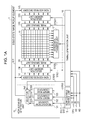
- Figs. 1A and 1B illustrate an exemplary configuration of a solid-state image pickup device.
- Figs. 2A and 2B are schematic timing diagrams illustrating a method of driving the solid-state image pickup device.
- Fig. 3 is a block diagram illustrating an exemplary configuration of a row counter control unit according to a first embodiment.
- Fig. 4 is a timing diagram illustrating the operation of the solid-state image pickup device according to the first embodiment.
- Fig. 5 is a block diagram illustrating an exemplary configuration of a row counter control unit according to a second embodiment.
- Fig. 6 is a timing diagram illustrating the operation of the solid-state image pickup device according to the second embodiment.
- FIG. 1A is a block diagram illustrating an exemplary configuration of a solid-state image pickup device according to a first embodiment of the present invention.
- a solid-state image pickup element 1 includes a pixel portion 11 and pixel driving units 12L and 12R.
- the pixel portion 11 is formed of a plurality of pixels arranged in a two-dimensional array of rows and columns.
- the pixel driving units 12L and 12R generate, respectively for odd-numbered rows and even-numbered rows, signals for driving the pixels, in other words, a transfer signal for transferring electric charges accumulated in photodiodes, and a row selection signal for selecting the pixels of a specific row of the array, for example.
- the pixel portion 11 includes the plurality of pixels each generating a pixel signal through photoelectric conversion performed by a photoelectric conversion element (photodiode).
- Each pixel may be an amplification-type pixel including a photoelectric conversion element and an amplifier unit for outputting a voltage signal based on the charge accumulated in the photoelectric conversion element, for example.
- the solid-state image pickup element 1 includes selection memory units 13L and 13R for respectively storing row selection signals for the odd and even-numbered rows, row address decoders 14L and 14R for selecting one row corresponding to a row count value S15, a row address generation unit 15, a timing generation unit 16, and a row counter control unit 18.
- the row address generation unit 15 includes a readout row counter 151, a reset row counter A (152), a reset row counter B (153), and a selector 150.
- the selector 150 selects one of the row addresses output from the three row counters 151 to 153 and outputs it as the row count value S15.
- the readout row counter 151 generates a readout row address of the pixel portion 11.
- the first reset row counter A (152) generates a row address indicating a row to be reset in an odd-numbered field (first field) of the pixel portion 11.
- the second reset row counter B (153) generates a row address indicating a row to be reset in an even-numbered field (second field) of the pixel portion 11.
- the odd-numbered field and even-numbered field constitute one frame.
- the selector 150 selects one of the row addresses generated by the readout row counter 151, the reset row counter A (152), and the reset row counter B (153).
- the row counter control unit 18 outputs counter control signals S1811 to S1813, such as counter start pulses, respectively to the three row counters 151 to 153, base on a communication signal 19, a vertical synchronization (VD) signal 20, and a horizontal synchronization (HD) signal 21 from an external CPU.
- the row counter control unit 18 controls the row counters 151 to 153.
- the row address decoders 14L and 14R decode a row address selected by the selector 150.
- the selection memory units 13L and 13R receive output bits from the row address decoders 14L and 14R, and store the states thereof.
- the pixel driving units 12L and 12R output row selection signals corresponding to the output bits stored in the selection memory units 13L and 13R.
- the timing generation unit 16 generates a row address generation unit selection signal S1610 for selecting one of the three row counters 151 to 153 on the basis of the communication signal 19 from an external CPU, the vertical synchronization signal 20, and the horizontal synchronization signal 21. Further, the timing generation unit 16 generates a memory unit control signal S162 which is common to the odd-numbered rows and even-numbered rows and controls the selection memory units 13L and 13R, and pixel driving signals S163L and S163R for controlling the pixel driving units 12L and 12R.
- the first pixel driving unit 12L selects an odd-numbered row of the pixel portion 11 corresponding to a row address selected by the selector 150.
- the second pixel driving unit 12R selects an even-numbered row of the pixel portion 11 corresponding to a row address selected by the selector 150.
- the first and second pixel driving units 12L and 12R are configured to control the operations of the pixels through logical sums or logical products of the outputs of the corresponding selection memory units 13L and 13R and a signal, which is not illustrated, provided from the timing generation unit 16.
- the solid-state image pickup element 1, the timing generation unit 16, and the row counter control unit 18 may or may not be integrated on the same semiconductor.
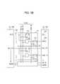
- Fig. 1B is a circuit diagram illustrating an exemplary configuration of the selection memory units 13L and 13R illustrated in Fig. 1A .
- Each of the selection memory units 13L and 13R includes row selection storage circuits 131 provided in a number equal to half the number of rows of the pixel portion 11.
- the row selection storage circuit 131 is configured to include a D latch 135, a logical product (AND) circuit 136, and an SR latch 137.
- Input to the row selection storage circuits 131 are one bit of a decoded signal 132 output from the row address decoders 14L and 14R, a write enable signal wen_rd, a clear signal clear_sh for clearing the SR latch 137, and a set signal wen_sh, which are the memory unit control signals S162.
- the write enable signal wen_rd is input to a clock terminal (CK) of the D latch 135, one bit within the decoded signal 132 is input to a data terminal (D), and a Q output signal of the D latch 135 becomes a row selection signal Lrd (133).
- the clear signal clear_sh is input to a reset terminal (R) of the SR latch 137.
- the set signal wen_sh and one bit within the decoded signal 132 are input to the AND circuit 136 and the logical product thereof are output to a set terminal (S) of the SR latch 137.
- the Q output signal of the SR latch 137 becomes a row selection signal Lsh (134) for selecting a row whose pixels are to be reset.
- the row selection signals Lrd (133) for selecting rows whose pixel signals are to be transferred, generated respectively in the selection memory units 13L and 13R, and the row selection signals Lsh (134) for selecting rows whose pixels are to be reset are input to the pixel driving units 12L and 12R. Thereby the pixel signals of the corresponding rows of the pixel portion 11 selected by the row address decoders 14L and 14R can be transferred and reset.
- Figs. 2A and 2B are schematic timing diagrams illustrating the operations of the row counter control unit 18 illustrated in Fig. 1A , the timing generation unit 16, and the selection memory units 13L and 13R.
- Fig. 2A illustrates input timings of externally input signals.
- the communication signal 19 from a CPU which is prior to a pulse 201 input as the vertical synchronization (VD) signal 20, includes a communication signal 191 for an operation to be performed during the next vertical synchronization period 203.
- the vertical synchronization period 203 is formed of a plurality of horizontal synchronization pulses 211 input as the horizontal synchronization (HD) signal 21.
- Fig. 2B is a schematic timing diagram illustrating a method of driving the solid-state image pickup device during a single horizontal synchronization period 212 illustrated in Fig. 2A .
- the operation during the horizontal synchronization period 212 is roughly divided into processing periods 221 to 225 illustrated as state transition 22.
- the row count value S15 becomes an output signal S151 of the readout row counter 151 during period 221 as a result of a row address generation unit selection signal S1610 of the timing generation unit 16, and becomes an output signal S152 of the reset row counter A (152) during period 222.
- the row count value S15 becomes an output signal S153 of the reset row counter B (153) in other periods.
- the timing generation unit 16 generates a pulse of the write enable signal wen_rd.
- the decoded signal 132 of the output signal S151 of the readout row counter 151 is latched by the D latch 135.
- the illustrated example is a case in which the output signal S151 of the readout row counter 151 selects rows L.
- the level of the row selection signal Lrd (133) indicating a row whose pixel signal is to be transferred goes high only for rows L, whereas those for other rows, rows (L + 1) to N, remain low.
- the row count value S15 is common to the row address decoders 14L and 14R, and the write enable signal wen_rd is also common to the selection memory units 13L and 13R.
- the pixel driving units 12L and 12R select respectively row L from among the group of only odd-numbered rows and row L from among the group of only even-numbered rows.
- the pixel driving unit 12L is controlled by the timing generation unit 16, and pixel signals of row L of the group of only odd-numbered rows in the pixel portion 11 are vertically transferred to a horizontal transfer unit 17.
- the pixel driving unit 12R is controlled by the timing generation unit 16, and pixel signals of row L of the group of only even-numbered rows in the pixel portion 11 are vertically transferred to a horizontal transfer unit 17.
- the pixel signals of row L of the odd-numbered rows and row L of the even-numbered rows which have been vertically transferred under the control of the timing generation unit 16 are horizontally transferred in the horizontal transfer unit 17 and become an output pixel signal of the solid-state image pickup element 1.
- the timing generation unit 16 generates a pulse of the clear signal clear_sh during period 221, and generates a pulse of the set signal wen_sh during period 222 and period 223.
- the illustrated example is an example in which an output signal S152 of the reset row counter A (152) selects rows L + 1, the output signal S153 of the reset row counter B (153) selects rows N, and rows L have been selected in the previous horizontal synchronization period 212.
- the level of Lsh [N] changes from a low level to a high level due to the output of the AND circuit 136, which receives, as inputs, the set signal wen_sh and the decoded signal 132 obtained by decoding row N selected by the output signal S153 of the reset row counter B (153).
- the row count value S15 is common to the row address decoders 14L and 14R, and the clear signal clear_sh, and the set signal wen_sh are also common to the selection memory units 13L and 13R.
- the pixel driving units 12L and 12R respectively select row L + 1 of the odd-numbered rows and row L + 1 of the even-numbered rows, and respectively select row N of the odd-numbered rows and row N of the even-numbered rows.
- the pixel driving units 12L and 12R are controlled by the timing generation unit 16, and the pixels of the selected row L +1 of the odd-numbered rows and row L + 1 of the even-numbered rows of the pixel portion 11, and the pixels of row N of the odd-numbered rows and row N of the even-numbered rows of the pixel portion 11 are reset.
- a pair of neighboring odd-numbered and even-numbered rows can be read, and two pairs of neighboring odd-numbered and even-numbered rows can be reset, during the horizontal synchronization period 212.
- FIG. 3 illustrates an exemplary configuration of the row counter control unit 18 according to the first embodiment.
- a CPU write register R (401) is a register for control of the readout row counter 151 performed through communication started by the CPU 19.
- the CPU write register R (401) stores a readout scan flag, a readout start row, a readout end row, and a step value for counting up performed by the readout row counter.
- a CPU write register A (402) is a register for controlling the reset row counter A (152) performed through communication from the CPU 19, and stores a reset scan start count, a reset start row, a reset end row, and a step value for counting up performed by the reset row counter A.
- a CPU write register B (403) is a register for control of the reset row counter B (153) performed through communication started by the CPU 19, and stores a reset scan start count, a reset start row, a reset end row, and a step value for counting up performed by the reset row counter B.
- a counter start pulse generation circuit R (407), when the readout scan flag stored in the CPU write register A (402) is not "0" (scanning is off), generates a start pulse 415 of the readout row counter 151 at the timing of the vertical synchronization signal 20.
- the readout end row and the step value for counting up performed by the readout row counter, stored in the CPU write register R (401), are copied and stored in a VD synchronization register R (408), and are input to the readout row counter 151 through a signal line 416.
- the reset scan start count, the reset end row, the step value for counting up performed by the reset row counter A, stored in the CPU write register A (402) are copied and stored in a VD synchronization register A (409).
- An HD counter 414 is a counter which is reset at the timing of the vertical synchronization signal 20, and performs counting up at the timing of the horizontal synchronization signal 21.
- a counter start pulse generation circuit A (417) and an HD counter synchronization register A (419) perform the following operations.
- the counter start pulse generation circuit A (417) generates a start pulse 418 for the reset row counter A (152).
- the reset end row and the step value for counting up performed by the reset row counter A, stored in the VD synchronization register A (409), are copied and stored in the HD counter synchronization register A (419) and output to the reset row counter A (152) as a register value 420.
- a counter start pulse generation circuit B (421) and an HD counter synchronization register B (423) perform the following operations.
- the counter start pulse generation circuit B (421) generates a start pulse 422 for the reset row counter B (153).
- the reset end row and the step value for counting up performed by the reset row counter B, stored in the VD synchronization register B (410), are copied and stored in the HD counter synchronization register B (423) and output to the reset row counter B (153) as a register value 424.
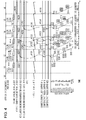
- Fig. 4 is a timing diagram illustrating the operation of the row counter control unit 18 according to the first embodiment illustrated in Fig. 3 , and the operations of the readout row counter 151, the reset row counter A (152), and the reset row counter B (153) based on the control signal output from the row counter control unit 18.
- Fig. 4 illustrates the operations of respective portions while a vertical synchronization period 500 proceeds from period V0 to period V6 due to the vertical synchronization signal 20.
- a CPU write register value 501 shows the timings at which writing is performed for the CPU write register R (401), the CPU write register A (402), and the CPU write register B (403) through communication started by the CPU 19.
- a VD synchronization register value 502 shows the timings at which the content of the CPU write register value 501 is copied to the VD synchronization register R (408), the VD synchronization register A (409), and the VD synchronization register B (410) in synchronization with the vertical synchronization signal 20.
- An HD counter value (413) illustrates how the count value of the counter which is the output of the HD counter 414 counts up, and the count value is reset to zero in synchronization with the vertical synchronization signal 20, and counts up by one every time the horizontal synchronization signal 21 is input.
- the HD counter synchronization register A value 420 is an output of the HD counter synchronization register A (419) and shows the times at which the content of the VD synchronization register A (409) is copied with reference to the HD counter value (413).
- the HD counter synchronization register B value 424 is an output of the HD counter synchronization register B (423) and shows the times at which the content of the VD synchronization register B (410) is copied with reference to the HD counter value (413).
- the counter start pulse R output (415) shows the pulse output times of the counter start pulse generation circuit R (407).
- the counter start pulse A output (418) shows the pulse output timings of the counter start pulse generation circuit A (417).
- the counter start pulse B output (422) shows the pulse output timings of the counter start pulse generation circuit B (421).
- Row address 503 shows the respective addresses of the rows of the pixel portion 11, in correspondence with the row count values S15 which are input for the row address decoders 14L and 14R.
- row 1 of the row address 503 corresponds to the count value 0 for the row address decoder 14L
- row 2 of the row address 503 corresponds to the count value 0 for the row address decoder 14R.
- Reset scans A (505, 509) show reset scans performed by the reset row counter A (152).
- reset scans B (08, 512) show reset scans performed by the reset row counter B (153)
- readout scans 506, 510, 513, and 514 show readout scans performed by the readout row counter 151.
- a readout scan flag is set to "0" (scan is off) in the CPU write register R (401) so as to instruct prohibition of a readout scan.
- An HD counter value (4131) is written into the CPU write register A (402) as a reset scan start count.
- "0" is written as a reset start row
- "n/2 - 1” is written as a reset end row
- "2" is written as a step value for counting up performed by the reset row counter A.
- a value larger than the HD counter value (413) corresponding to one vertical synchronization period is set as a reset scan start count, whereby a reset scan can be practically prohibited.
- the respective CPU write register values 501 written through the communication 5011 are copied (5021) to the VD synchronization register R (408), the VD synchronization register A (409), and the VD synchronization register B (410). Then, when the HD counter value (413) matches the HD counter value (4131), which is the reset scan start count stored in the VD synchronization register A (409), the VD synchronization register A (409) is copied (4201) to the HD counter synchronization register A (419). Further, the counter start pulse generation circuit A (417) generates a start pulse 4181 for the reset row counter A (152). Upon receipt of the start pulse 4181, the reset row counter A (152) starts the reset scan A (505).
- the reset row counter A (152) refers to an HD counter synchronization register A value (4201).
- the reset row counter A (152) starts counting from "0", which is a reset start row, and resets rows 1 and 2 of the pixel portion 11 (5051, 5052).
- the reset row counter A (152) outputs a value, to which the step value "2" for counting up has been added, and resets rows 5 and 6 of the pixel portion 11 (5053, 5054).
- the reset scans are performed until the reset end row "n/2 - 1" is reached, by adding the step value "2" for every horizontal synchronization period.
- the CPU write register value 501 written through communication 5012 is copied (5022) to the VD synchronization register.
- the counter start pulse generation circuit R (407) generates a start pulse 4151, since the readout scan flag is "1" (scan is on).
- the readout row counter 151 starts a readout scan (506) on the basis of the settings of the readout start row "0", the readout end row "n/2 - 1", and the step up value "2" for counting up performed by the readout counter.
- the readout scan (506) is a process of reading odd-numbered field 1 of the pixel portion 11 which has been reset by the reset scan A (505), and a time difference between the reset scan A (505) and the readout scan (506) is an exposure period 507.
- the VD synchronization register B (410) is copied (4241) to the HD counter synchronization register B (423).
- the counter start pulse generation circuit B (421) generates a start pulse 4182 for the reset row counter B (153).
- the reset row counter B (153) starts a reset scan B (508) on the basis of the reset start row "1", the reset end row "n/2", and the step value "2" for counting up.
- the pixels of the even-numbered field formed of rows 3, 4, 7, 8, ⁇ are reset.
- the VD synchronization register A (409) is copied (4202) to the HD counter synchronization register A (419). Further, the counter start pulse generation circuit A (417) generates a start pulse 4152 for the reset row counter A (152). Upon receipt of the start pulse 4152, the reset row counter A (152) starts a reset scan A (509). The pixels of the odd-numbered field formed of rows 1, 2, 5, 6, ⁇ are reset.
- the readout scan 513 is a process of reading odd-numbered field 2 of the pixel portion 11 which has been reset by the reset scan A (509), and a time difference between the reset scan A (509) and the readout scan 513 is an exposure period 511.
- setting is possible such that the exposure period 507 is shorter than the vertical synchronization period, whereas the exposure period 511 is longer than the vertical synchronization period, and this can be controlled by the timing, for the reset operation, of the communication signal 19 from the CPU.
- the communication 5012 for the readout scan 506 for the exposure period 507 is in period V2 and the communication 5011 for the corresponding reset scan A (505) is in period V1, and hence the difference is one vertical scan period.
- the communication 5014 for the readout scan 513 is during period V4
- the communication 5012 for the corresponding reset scan A (509) is performed in period V2, that is, two vertical scan periods in advance
- the exposure period 511 is obtained.
- the reset scan 509 of odd-numbered field 2 is performed before the readout scan 510 of even-numbered field 1.
- scanning is performed in the reset scan 509 such that the readout rows of even-numbered field 1 are skipped due to the step value "2" for counting up, the readout rows of even-numbered field 1 are not reset before being read.
- the pixel driving units 12L and 12R select the rows of the pixel portion 11 as a pair of one odd-numbered row and one neighboring even-numbered row in accordance with a row address selected by the selector 150.
- the exposure period 507 in a shorter accumulation period operation is shorter than one vertical synchronization period, and is short compared with one field cycle.
- odd-numbered pairs of rows of the pixel portion 11 selected by the pixel driving units 12L and 12R are sequentially scanned by the reset scan 505, and the pixel signals of the pixels of odd-numbered field 1 are reset.
- the odd-numbered pairs of rows of the pixel portion 11 selected by the pixel driving units 12L and 12R are sequentially scanned by the readout scan 506, and the pixel signals of the pixels of odd-numbered field 1 are read.
- even-numbered pairs of rows of the pixel portion 11 selected by the pixel driving units 12L and 12R are sequentially scanned, and the pixel signals of the pixels of even-numbered field 1 are reset.
- the even-numbered pairs of rows of the pixel portion 11 selected by the pixel driving units 12L and 12R are sequentially scanned, and the pixel signals of the pixels of even-numbered field 1 are read.
- the exposure period 511 in a longer accumulation period operation is longer than one vertical synchronization period, and is long compared to one field cycle.
- first operation mode a longer accumulation period operation
- odd-numbered pairs of rows of the pixel portion 11 selected by the pixel driving units 12L and 12R are sequentially scanned, and the pixel signals of the pixels of odd-numbered field 2 are reset.
- even-numbered pairs of rows of the pixel portion 11 selected by the pixel driving units 12L and 12R are sequentially scanned, and the pixel signals of the pixels of even-numbered field 2 are reset.
- the odd-numbered pairs of rows of the pixel portion 11 selected by the pixel driving units 12L and 12R are sequentially scanned, and the pixel signals of the pixels of odd-numbered field 2 are read.
- the even-numbered pairs of rows of the pixel portion 11 selected by the pixel driving units 12L and 12R are sequentially scanned, and the pixel signals of the pixels of even-numbered field 2 are read.
- the readout scan 510 for reading the pixel signals of the pixels of even-numbered field 1 in the shorter accumulation period operation is started after the reset scan 509 for resetting the pixel signals of the pixels of odd-numbered field 2 in the longer accumulation period operation has started.
- the readout scan 510 for reading the pixel signals of the pixels of even-numbered field 1 in the shorter accumulation period operation is started before the reset scan 512 for resetting the pixel signals of the pixels of even-numbered field 2 in the longer accumulation period operation is started.
- the readout row counter 151 generates the row address for interlaced readout of an odd-numbered field and an even-numbered field.
- the two reset row counters 152 and 153 perform the following operation.
- the two reset row counters 152 and 153 generate row addresses such that row resetting of the odd-numbered field and row resetting of the even-numbered field are performed so as to respectively skip the readout rows of the even-numbered field and the odd-numbered field.
- the row counter control unit 18 includes the first counter start pulse generation circuit R (407), the horizontal synchronization signal counter 414, the second counter start pulse generation circuit A (417), and the third counter start pulse generation circuit B (421).
- the first counter start pulse generation circuit R (407) generates the counter start pulse 415 for making the readout row counter 151 start counting.
- the second horizontal synchronization signal counter 414 is reset at the timing of the vertical synchronization signal 20 and counts up at the timing of the horizontal synchronization signal 21.
- the counter start pulse generation circuit A (417) in accordance with the counter value of the horizontal synchronization signal counter 414, generates the counter start pulse 418 for making the reset row counter A (152) start counting.
- the third counter start pulse generation circuit B (421) in accordance with the counter value of the horizontal synchronization signal counter 414, generates the counter start pulse 422 for making the second reset row counter B (153) start counting.
- a solid-state image pickup device according to a second embodiment of the present invention will be described centering around the difference from the first embodiment.
- the configuration of the solid-state image pickup device in the present embodiment is the same as that illustrated in Fig. 1A , and operations other than the row counter control unit 18 are also the same as those in the first embodiment.
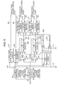
- Fig. 5 illustrates an exemplary configuration of a row counter control unit 18 according to the second embodiment.
- a field determination circuit 604 outputs a field determination result 605 which alternately changes between "0" and "1" in synchronization with the vertical synchronization signal 20.
- the operations of the CPU write register R (401), the counter start pulse generation circuit R (407), and the VD synchronization register R (408) are the same as those described referring to Fig. 3 .
- a register is added for storing an offset value which is a difference in readout start row between a reference odd-numbered field and an even-numbered field.
- a CPU write register S (601) is a setting register common to the reset row counter A (152) and the reset row counter B (153).
- the CPU write register S (601) stores a reset scan start count, a reset start row, a reset end row, a step value for counting up, and an offset value which is a difference in reset start row between a reference odd-numbered field and an even-numbered field.
- An HD counter A (606) is a counter which is reset at the timing of the vertical synchronization signal 20 only when the field determination result 605 is "0", and performs counting up at the timing of the horizontal synchronization signal 21.
- An HD counter B (608) is a counter which is reset at the timing of the vertical synchronization signal 20 only when the field determination result 605 is "1", and performs counting up at the timing of the horizontal synchronization signal 21. Note that the HD counter A (606) and the HD counter B (608) are counters which can count the number of pulses of the horizontal synchronization signal 21 which are input during two vertical synchronization periods.
- the counter start pulse generation circuit A (417) and the HD counter synchronization register A (419) perform the same operations as described referring to Fig.
- the counter start pulse generation circuit B (421) and the HD counter synchronization register B (423) perform the same operations as described referring to Fig. 3 , except that an output signal (HD counter B value) 609 of the HD counter B (608) is referred to in the present embodiment.
- Fig. 6 is a timing diagram illustrating the operation of the row counter control unit 18 according to the second embodiment and the operations of the readout row counter 151, the reset row counter A (152), and the reset row counter B (153) based on the control signal of the row counter control unit 18.
- the HD counter A value (607) is reset in synchronization with the vertical synchronization signal 20 when the field determination result 605 is "0", and performs counting up at every input of the horizontal synchronization signal 21.
- the HD counter B value (609) is reset in synchronization with the vertical synchronization signal 20 when the field determination result 605 is "1" and performs counting up at every input of the horizontal synchronization signal 21.
- the operations and timings of the counter start pulse R output (415), the counter start pulse A output (418), the counter start pulse B output (422), the reset scans A (505, 509), and the reset scans B (508, 512) are the same as those illustrated in Fig. 3 .
- the operations and timings of the readout scans 506, 510, 513, and 514 are also the same as those illustrated in Fig. 3 .
- a readout scan flag is set to "0" (scan is off) in the CPU write register R (401) so as to instruct prohibition of a readout scan.
- the HD counter value A (6071) is written into the CPU write register S (601) as a reset scan start count.
- "0" is written as a reset start row
- "n/2 - 1" is written as a reset end row
- "2" is written as a step value for counting up
- "1" is written as an offset value.
- a reset scan start count value 6071 is larger than the number of pulses of the horizontal synchronization signal 21 input during one vertical synchronization period.
- the value of the CPU write register R (401) is copied (4081) to the VD synchronization register R (408) in synchronization with the vertical synchronization signal 20. Since the field determination result 605 is "0" at the input timing of the vertical synchronization signal 20 during period V1, the value of the CPU write register S (601) is copied (4111) to the VD synchronization register A (409) through the switch 603A. On the other hand, the VD synchronization register B (410) holds the current value, since copying is not performed through the switch 603B. However, the value of the CPU write register S (601) is copied (4121) to the VD synchronization register B (410) at the timing when the field determination result 605 becomes "1" during period V2. At this time, values to which an offset value has been added is stored in the VD synchronization register B (410) as a reset start row and a reset end row.
- a reset scan start count value 6072 is smaller than the number of pulses of the horizontal synchronization signal 21 input during one vertical synchronization period.
- a CPU write register value 701 as a result of communication 7012 is copied (4082) to the VD synchronization register R 408.
- the CPU write register value 701 is copied to the VD synchronization register A (409) but not to the VD synchronization register B (410).
- the counter start pulse generation circuit R (407) generates the start pulse 4151.
- the readout row counter 151 starts the readout scan (506) on the basis of the readout start row "0", the readout end row "n/2 - 1", and the step value "2" for counting up performed by the readout row counter.
- the HD counter value B (609) matches the reset scan start count value (6071), which is the reset scan start count stored in the VD synchronization register B (410)
- the value of the VD synchronization register B (410) is copied (4241) to the HD counter synchronization register B (423).
- the counter start pulse generation circuit B (421) generates the start pulse 4182 for the reset row counter B (153).
- the reset row counter B (153) starts the reset scan B (508) on the basis of the reset start row "1" and the reset end row of "n/2", after addition of the offset, and the count up step value "2".
- the HD counter A value 607 matches the reset scan start count value (6072) of the VD synchronization register A (409), which is a reset scan start count stored in the VD synchronization register A (409)
- the value of the VD synchronization register A (409) is copied (4202) to the HD counter synchronization register A (419).
- the counter start pulse generation circuit A (417) generates the start pulse 4152 for the reset row counter A (152).
- the reset row counter A (152) starts the reset scan A (509).
- the CPU write register value 701 as a result of the communication 7012 during period V3, is copied (4083) to the VD synchronization register R (408).
- the field determination result 605 is "1”
- an offset value of "1” is added to the readout start row and readout end row stored in the VD synchronization register R 408.
- the VD synchronization register A (409) is not copied, and the offset value "1” is added in the VD synchronization register B (410).
- the counter start pulse generation circuit R (407) since the readout scan flag is "1" (scan is on), generates a start pulse 4153.
- the readout row counter 151 starts the readout scan (510) using the readout start row "1" and readout end row "n/2" to which the offset has been added.
- the HD counter B value (609) matches the reset scan start count value (6072), which is the reset scan start count stored in the VD synchronization register B (410)
- the value of the VD synchronization register B (410) is copied (4242) to the HD counter synchronization register B (423).
- the counter start pulse generation circuit B (421) generates a start pulse 4183 for the reset row counter B (153).
- the reset row counter B (153) starts the reset scan B (512) on the basis of the reset start row "1" and the reset end row "n/2", after addition of the offset, and the count up step value "2".
- the row counter control unit 18 includes the first counter start pulse generation circuit R (407), the second counter start pulse generation circuit A (417), and the third counter start pulse generation circuit B (421). Further, the row counter control unit 18 includes the first horizontal synchronization signal counter A (606) and the second horizontal synchronization signal counter B (608).
- the first counter start pulse generation circuit R (407) generates the counter start pulse 415 for making the readout row counter 151 start counting.
- the first horizontal synchronization signal counter A (606) is reset at the timing of every two vertical synchronization signals 20, and is made to perform counting up at the timing of the horizontal synchronization signal 21.
- the second horizontal synchronization signal counter B (608) is reset at the timing of every two vertical synchronization signals 20 and with an offset of one vertical synchronization signal 20 with respect to the HD counter A (606), and made to perform counting up at the timing of the horizontal synchronization signal 21.
- the second counter start pulse generation circuit A (417) generates the counter start pulse 418 for making the first reset row counter A (152) start counting in accordance with the count value of the first horizontal synchronization signal counter A (606).
- the third counter start pulse generation circuit B (421) generates the counter start pulse 422 for making the second reset row counter B (153) start counting in accordance with the counter value of the second horizontal synchronization signal counter B (608).
- the solid-state image pickup devices of the first and second embodiments can be used as solid-state image pickup devices for digital cameras and the like. According to the first and second embodiments, switching of thinning-out methods of readout in the pixel portion 11 is not performed between the case in which setting of an accumulation period within one vertical scan period for a shorter accumulation period operation is required and the case in which setting of an accumulation period exceeding one vertical scan period for a longer accumulation period operation is required. This enables shooting of natural-looking moving images without a change in the image quality before and after switching between a shorter accumulation period operation and a longer accumulation period operation. In addition, the image quality in moving image shooting at times of low illuminance is improved, and simplified control thereof is realized.
- sets of two of the row address decoders 14, the selection memory units 13, and the pixel driving units 12 are provided.
- the pixel portion 11 may be controlled using just one component from each set.
- the total number of decoded values which can be output from a row address decoder becomes double that in the above-described embodiments.
- the number of components is large since the selection memory units 13 are formed of logic circuits, latch circuits, and the like.
- the pixels become finer, it becomes more advantageous for realizing easier layout to provide sets of two of the row address decoders 14, the selection memory units 13, and the pixel driving units 12, as illustrated.
- each row may of course be independently selected.
- first field odd-numbered field
- second field even-numbered field
- a solid-state image pickup device that includes: a pixel portion (11) having a plurality of pixels that are arranged in a two-dimensional array and generate pixel signals; a readout row counter (151) that generates a row address for reading the pixel portion; a first reset row counter (152) that generates row addresses for resetting a first field of the pixel portion; a second reset row counter (153) that generates a row address for resetting a second field of the pixel portion; a selector (150) that selects one of the row addresses generated by the readout row counter, the first reset row counter, and the second reset row counter; and pixel driving units (12L, 12R) that respectively select two rows: an odd-numbered row and a neighboring even-numbered row of the
Landscapes
- Engineering & Computer Science (AREA)
- Multimedia (AREA)
- Signal Processing (AREA)
- Transforming Light Signals Into Electric Signals (AREA)
Abstract
Description
- The present invention relates to solid-state devices and methods of driving the devices.
- Recently, solid-state image pickup devices including more than millions of pixels have been used for digital cameras, allowing high precision still images to be captured. Also in the case of shooting moving images, it is required that solid-state image pickup devices read out images at high frame rates to enable moving images to be shot without jerkiness. In the case of high-rate reading, since an image accumulation period per frame of photoelectric conversion elements in the pixel portion of a solid-state image pickup device is short, there is a problem in that sufficient exposure amounts are not obtained particularly for dark objects. As means for obtaining sufficient exposure amounts with a limited exposure period, Japanese Patent Laid-Open No.
2006-74440 2006-74440 - In the solid state image pickup device disclosed in Japanese Patent Laid-Open No.
2006-74440 2006-74440 - The present invention in its first aspect provides an exposure apparatus as specified in
claims 1 to 7. - The present invention in its second aspect provides an exposure method as specified in
claims 8 to 15. - Further features of the present invention will become apparent from the following description of exemplary embodiments (with reference to the attached drawings).
-
Figs. 1A and1B illustrate an exemplary configuration of a solid-state image pickup device. -
Figs. 2A and 2B are schematic timing diagrams illustrating a method of driving the solid-state image pickup device. -
Fig. 3 is a block diagram illustrating an exemplary configuration of a row counter control unit according to a first embodiment. -
Fig. 4 is a timing diagram illustrating the operation of the solid-state image pickup device according to the first embodiment. -
Fig. 5 is a block diagram illustrating an exemplary configuration of a row counter control unit according to a second embodiment. -
Fig. 6 is a timing diagram illustrating the operation of the solid-state image pickup device according to the second embodiment. -
Fig. 1A is a block diagram illustrating an exemplary configuration of a solid-state image pickup device according to a first embodiment of the present invention. A solid-stateimage pickup element 1 includes apixel portion 11 andpixel driving units pixel portion 11 is formed of a plurality of pixels arranged in a two-dimensional array of rows and columns. Thepixel driving units pixel portion 11 includes the plurality of pixels each generating a pixel signal through photoelectric conversion performed by a photoelectric conversion element (photodiode). Each pixel may be an amplification-type pixel including a photoelectric conversion element and an amplifier unit for outputting a voltage signal based on the charge accumulated in the photoelectric conversion element, for example. The solid-stateimage pickup element 1 includesselection memory units row address decoders address generation unit 15, atiming generation unit 16, and a rowcounter control unit 18. The rowaddress generation unit 15 includes areadout row counter 151, a reset row counter A (152), a reset row counter B (153), and aselector 150. Theselector 150 selects one of the row addresses output from the threerow counters 151 to 153 and outputs it as the row count value S15. Thereadout row counter 151 generates a readout row address of thepixel portion 11. The first reset row counter A (152) generates a row address indicating a row to be reset in an odd-numbered field (first field) of thepixel portion 11. The second reset row counter B (153) generates a row address indicating a row to be reset in an even-numbered field (second field) of thepixel portion 11. The odd-numbered field and even-numbered field constitute one frame. Theselector 150 selects one of the row addresses generated by thereadout row counter 151, the reset row counter A (152), and the reset row counter B (153). The rowcounter control unit 18 outputs counter control signals S1811 to S1813, such as counter start pulses, respectively to the threerow counters 151 to 153, base on acommunication signal 19, a vertical synchronization (VD)signal 20, and a horizontal synchronization (HD)signal 21 from an external CPU. The rowcounter control unit 18 controls therow counters 151 to 153. Therow address decoders selector 150. Theselection memory units row address decoders pixel driving units selection memory units timing generation unit 16 generates a row address generation unit selection signal S1610 for selecting one of the threerow counters 151 to 153 on the basis of thecommunication signal 19 from an external CPU, thevertical synchronization signal 20, and thehorizontal synchronization signal 21. Further, thetiming generation unit 16 generates a memory unit control signal S162 which is common to the odd-numbered rows and even-numbered rows and controls theselection memory units pixel driving units pixel driving unit 12L selects an odd-numbered row of thepixel portion 11 corresponding to a row address selected by theselector 150. The secondpixel driving unit 12R selects an even-numbered row of thepixel portion 11 corresponding to a row address selected by theselector 150. The first and secondpixel driving units selection memory units timing generation unit 16. The solid-stateimage pickup element 1, thetiming generation unit 16, and the rowcounter control unit 18 may or may not be integrated on the same semiconductor. -
Fig. 1B is a circuit diagram illustrating an exemplary configuration of theselection memory units Fig. 1A . Each of theselection memory units selection storage circuits 131 provided in a number equal to half the number of rows of thepixel portion 11. The rowselection storage circuit 131 is configured to include aD latch 135, a logical product (AND)circuit 136, and anSR latch 137. Input to the rowselection storage circuits 131 are one bit of a decodedsignal 132 output from therow address decoders SR latch 137, and a set signal wen_sh, which are the memory unit control signals S162. The write enable signal wen_rd is input to a clock terminal (CK) of theD latch 135, one bit within thedecoded signal 132 is input to a data terminal (D), and a Q output signal of theD latch 135 becomes a row selection signal Lrd (133). The clear signal clear_sh is input to a reset terminal (R) of theSR latch 137. The set signal wen_sh and one bit within thedecoded signal 132 are input to theAND circuit 136 and the logical product thereof are output to a set terminal (S) of theSR latch 137. The Q output signal of theSR latch 137 becomes a row selection signal Lsh (134) for selecting a row whose pixels are to be reset. The row selection signals Lrd (133) for selecting rows whose pixel signals are to be transferred, generated respectively in theselection memory units pixel driving units pixel portion 11 selected by therow address decoders -
Figs. 2A and 2B are schematic timing diagrams illustrating the operations of the rowcounter control unit 18 illustrated inFig. 1A , thetiming generation unit 16, and theselection memory units Fig. 2A illustrates input timings of externally input signals. Thecommunication signal 19 from a CPU, which is prior to a pulse 201 input as the vertical synchronization (VD)signal 20, includes acommunication signal 191 for an operation to be performed during the nextvertical synchronization period 203. Thevertical synchronization period 203 is formed of a plurality ofhorizontal synchronization pulses 211 input as the horizontal synchronization (HD)signal 21. -
Fig. 2B is a schematic timing diagram illustrating a method of driving the solid-state image pickup device during a singlehorizontal synchronization period 212 illustrated inFig. 2A . The operation during thehorizontal synchronization period 212 is roughly divided intoprocessing periods 221 to 225 illustrated asstate transition 22. The row count value S15 becomes an output signal S151 of thereadout row counter 151 duringperiod 221 as a result of a row address generation unit selection signal S1610 of thetiming generation unit 16, and becomes an output signal S152 of the reset row counter A (152) duringperiod 222. The row count value S15 becomes an output signal S153 of the reset row counter B (153) in other periods. - First, the operation of transferring pixel signals of a row during the
horizontal synchronization period 212 is described. First, duringperiod 221, thetiming generation unit 16 generates a pulse of the write enable signal wen_rd. The decodedsignal 132 of the output signal S151 of thereadout row counter 151 is latched by theD latch 135. Here, the illustrated example is a case in which the output signal S151 of thereadout row counter 151 selects rows L. The level of the row selection signal Lrd (133) indicating a row whose pixel signal is to be transferred goes high only for rows L, whereas those for other rows, rows (L + 1) to N, remain low. At this time, the row count value S15 is common to therow address decoders selection memory units pixel driving units period 222, thepixel driving unit 12L is controlled by thetiming generation unit 16, and pixel signals of row L of the group of only odd-numbered rows in thepixel portion 11 are vertically transferred to ahorizontal transfer unit 17. Duringperiod 223, thepixel driving unit 12R is controlled by thetiming generation unit 16, and pixel signals of row L of the group of only even-numbered rows in thepixel portion 11 are vertically transferred to ahorizontal transfer unit 17. Duringperiod 225, the pixel signals of row L of the odd-numbered rows and row L of the even-numbered rows which have been vertically transferred under the control of thetiming generation unit 16 are horizontally transferred in thehorizontal transfer unit 17 and become an output pixel signal of the solid-stateimage pickup element 1. - Next, the reset operation of the pixel signals of a row during the
horizontal synchronization period 212 will be described. Thetiming generation unit 16 generates a pulse of the clear signal clear_sh duringperiod 221, and generates a pulse of the set signal wen_sh duringperiod 222 andperiod 223. Here, the illustrated example is an example in which an output signal S152 of the reset row counter A (152) selects rows L + 1, the output signal S153 of the reset row counter B (153) selects rows N, and rows L have been selected in the previoushorizontal synchronization period 212. - During
period 221, all the SR latches 137 are reset by the pulse of the clear signal clear_sh, and the level of Lsh [L], which has been selected, changes from a high level to a low level. Duringperiod 222, the level of Lsh [L +1] changes from a low level to a high level due to the output of the ANDcircuit 136, which receives, as inputs, the set signal wen_sh and the decodedsignal 132 obtained by decoding row L + 1 selected by the output signal S152 of the reset row counter A (152). Duringperiod 223, the level of Lsh [N] changes from a low level to a high level due to the output of the ANDcircuit 136, which receives, as inputs, the set signal wen_sh and the decodedsignal 132 obtained by decoding row N selected by the output signal S153 of the reset row counter B (153). At this time, the row count value S15 is common to therow address decoders selection memory units pixel driving units period 224, thepixel driving units timing generation unit 16, and the pixels of the selected row L +1 of the odd-numbered rows and row L + 1 of the even-numbered rows of thepixel portion 11, and the pixels of row N of the odd-numbered rows and row N of the even-numbered rows of thepixel portion 11 are reset. As a result, in the configuration described above, a pair of neighboring odd-numbered and even-numbered rows can be read, and two pairs of neighboring odd-numbered and even-numbered rows can be reset, during thehorizontal synchronization period 212. -
Fig. 3 illustrates an exemplary configuration of the rowcounter control unit 18 according to the first embodiment. Hereinafter, description is made of a method of driving the solid-state image pickup device allowing an accumulation time to be continuously set irrespective of whether the exposure period is shorter or longer than a vertical synchronization period. A CPU write register R (401) is a register for control of thereadout row counter 151 performed through communication started by theCPU 19. The CPU write register R (401) stores a readout scan flag, a readout start row, a readout end row, and a step value for counting up performed by the readout row counter. A CPU write register A (402) is a register for controlling the reset row counter A (152) performed through communication from theCPU 19, and stores a reset scan start count, a reset start row, a reset end row, and a step value for counting up performed by the reset row counter A. A CPU write register B (403) is a register for control of the reset row counter B (153) performed through communication started by theCPU 19, and stores a reset scan start count, a reset start row, a reset end row, and a step value for counting up performed by the reset row counter B. A counter start pulse generation circuit R (407), when the readout scan flag stored in the CPU write register A (402) is not "0" (scanning is off), generates astart pulse 415 of thereadout row counter 151 at the timing of thevertical synchronization signal 20. - At the timing of the
vertical synchronization signal 20, the readout end row and the step value for counting up performed by the readout row counter, stored in the CPU write register R (401), are copied and stored in a VD synchronization register R (408), and are input to thereadout row counter 151 through asignal line 416. At the timing of thevertical synchronization signal 20, the reset scan start count, the reset end row, the step value for counting up performed by the reset row counter A, stored in the CPU write register A (402) are copied and stored in a VD synchronization register A (409). At the timing of thevertical synchronization signal 20, the reset scan start count, the reset start row, the reset end row, and the step value for counting up performed by the reset row counter B, stored in the CPU write register B (403) are copied and stored in a VD synchronization register B (410). AnHD counter 414 is a counter which is reset at the timing of thevertical synchronization signal 20, and performs counting up at the timing of thehorizontal synchronization signal 21. - When the
horizontal synchronization signal 21 is continuously input and the count value of theHD counter 414 matches the reset scan start count stored in the VD synchronization register A (409), a counter start pulse generation circuit A (417) and an HD counter synchronization register A (419) perform the following operations. First, the counter start pulse generation circuit A (417) generates astart pulse 418 for the reset row counter A (152). The reset end row and the step value for counting up performed by the reset row counter A, stored in the VD synchronization register A (409), are copied and stored in the HD counter synchronization register A (419) and output to the reset row counter A (152) as aregister value 420. - Similarly, when the count value of the
HD counter 414 matches the reset scan start count stored in the VD synchronization register B (410), a counter start pulse generation circuit B (421) and an HD counter synchronization register B (423) perform the following operations. First, the counter start pulse generation circuit B (421) generates astart pulse 422 for the reset row counter B (153). The reset end row and the step value for counting up performed by the reset row counter B, stored in the VD synchronization register B (410), are copied and stored in the HD counter synchronization register B (423) and output to the reset row counter B (153) as aregister value 424. -
Fig. 4 is a timing diagram illustrating the operation of the rowcounter control unit 18 according to the first embodiment illustrated inFig. 3 , and the operations of thereadout row counter 151, the reset row counter A (152), and the reset row counter B (153) based on the control signal output from the rowcounter control unit 18.Fig. 4 illustrates the operations of respective portions while avertical synchronization period 500 proceeds from period V0 to period V6 due to thevertical synchronization signal 20. A CPUwrite register value 501 shows the timings at which writing is performed for the CPU write register R (401), the CPU write register A (402), and the CPU write register B (403) through communication started by theCPU 19. - A VD synchronization register value 502 shows the timings at which the content of the CPU write
register value 501 is copied to the VD synchronization register R (408), the VD synchronization register A (409), and the VD synchronization register B (410) in synchronization with thevertical synchronization signal 20. An HD counter value (413) illustrates how the count value of the counter which is the output of theHD counter 414 counts up, and the count value is reset to zero in synchronization with thevertical synchronization signal 20, and counts up by one every time thehorizontal synchronization signal 21 is input. The HD counter synchronizationregister A value 420 is an output of the HD counter synchronization register A (419) and shows the times at which the content of the VD synchronization register A (409) is copied with reference to the HD counter value (413). The HD counter synchronizationregister B value 424 is an output of the HD counter synchronization register B (423) and shows the times at which the content of the VD synchronization register B (410) is copied with reference to the HD counter value (413). The counter start pulse R output (415) shows the pulse output times of the counter start pulse generation circuit R (407). The counter start pulse A output (418) shows the pulse output timings of the counter start pulse generation circuit A (417). The counter start pulse B output (422) shows the pulse output timings of the counter start pulse generation circuit B (421). -
Row address 503 shows the respective addresses of the rows of thepixel portion 11, in correspondence with the row count values S15 which are input for therow address decoders row 1 of therow address 503 corresponds to thecount value 0 for therow address decoder 14L, androw 2 of therow address 503 corresponds to thecount value 0 for therow address decoder 14R. Reset scans A (505, 509) show reset scans performed by the reset row counter A (152). For example, in the reset scan A (505), it is shown thatreset rows row address decoder 14L, and resetrows row address decoder 14R. Similarly, reset scans B (508, 512) show reset scans performed by the reset row counter B (153), andreadout scans readout row counter 151. - The operation illustrated in
Fig. 4 will now be described. First, in period V1, throughcommunication 5011 started by theCPU 19, a readout scan flag is set to "0" (scan is off) in the CPU write register R (401) so as to instruct prohibition of a readout scan. An HD counter value (4131) is written into the CPU write register A (402) as a reset scan start count. Similarly, "0" is written as a reset start row, "n/2 - 1" is written as a reset end row, and "2" is written as a step value for counting up performed by the reset row counter A. In the CPU write register B (403), a value larger than the HD counter value (413) corresponding to one vertical synchronization period is set as a reset scan start count, whereby a reset scan can be practically prohibited. - During period V2, first, the respective CPU write
register values 501 written through thecommunication 5011 are copied (5021) to the VD synchronization register R (408), the VD synchronization register A (409), and the VD synchronization register B (410). Then, when the HD counter value (413) matches the HD counter value (4131), which is the reset scan start count stored in the VD synchronization register A (409), the VD synchronization register A (409) is copied (4201) to the HD counter synchronization register A (419). Further, the counter start pulse generation circuit A (417) generates a start pulse 4181 for the reset row counter A (152). Upon receipt of the start pulse 4181, the reset row counter A (152) starts the reset scan A (505). During the reset scan A (505), the reset row counter A (152) refers to an HD counter synchronization register A value (4201). During the horizontal synchronization period of the start pulse 4181, the reset row counter A (152) starts counting from "0", which is a reset start row, and resetsrows rows 5 and 6 of the pixel portion 11 (5053, 5054). After this, the reset scans are performed until the reset end row "n/2 - 1" is reached, by adding the step value "2" for every horizontal synchronization period. - Further, in period V2, the following is written into the CPU write register R (401) through communication 5012: "1" (scan is on) as a readout flag, "0" as a readout start row, "n/2 - 1" as a readout end row, and "2" as a step value for counting up performed by the readout row counter. The following is written into the CPU write register A (402): an HD counter value (4133) as a reset scan start count, "0" as a reset start row, "n/2 - 1" as a reset end row, and "2" as a step value for counting up performed by the reset row counter A. The following is written into the CPU write register B (403): an HD counter value (4132) as a reset scan start count, "1" as a reset start row, "n/2" as a reset end row, and "2" as a step value for counting up performed by the reset row counter A.
- During period V3, first, the CPU write
register value 501 written throughcommunication 5012 is copied (5022) to the VD synchronization register. The counter start pulse generation circuit R (407) generates astart pulse 4151, since the readout scan flag is "1" (scan is on). Upon receipt of thestart pulse 4151, the readout row counter 151 starts a readout scan (506) on the basis of the settings of the readout start row "0", the readout end row "n/2 - 1", and the step up value "2" for counting up performed by the readout counter. The readout scan (506) is a process of reading odd-numberedfield 1 of thepixel portion 11 which has been reset by the reset scan A (505), and a time difference between the reset scan A (505) and the readout scan (506) is anexposure period 507. - Next, when the HD counter value (413) matches an HD counter value (4132), which is the reset scan start count stored in the VD synchronization register B (410), the VD synchronization register B (410) is copied (4241) to the HD counter synchronization register B (423). Further, the counter start pulse generation circuit B (421) generates a
start pulse 4182 for the reset row counter B (153). Upon receipt of thestart pulse 4182, the reset row counter B (153) starts a reset scan B (508) on the basis of the reset start row "1", the reset end row "n/2", and the step value "2" for counting up. The pixels of the even-numbered field formed ofrows - Next, when the HD counter value (413) matches an HD counter value (4133), which is the reset scan start stored in the VD synchronization register A (409), the VD synchronization register A (409) is copied (4202) to the HD counter synchronization register A (419). Further, the counter start pulse generation circuit A (417) generates a
start pulse 4152 for the reset row counter A (152). Upon receipt of thestart pulse 4152, the reset row counter A (152) starts a reset scan A (509). The pixels of the odd-numbered field formed ofrows - After this, similarly, setting for a
readout scan 510 and a reset scan B (512) during period V4 is made throughcommunication 5013, and setting for areadout scan 513 during period V5 is made throughcommunication 5014, as is illustrated in the figure. Thereadout scan 513 is a process of reading odd-numberedfield 2 of thepixel portion 11 which has been reset by the reset scan A (509), and a time difference between the reset scan A (509) and thereadout scan 513 is anexposure period 511. Here, it is illustrated that setting is possible such that theexposure period 507 is shorter than the vertical synchronization period, whereas theexposure period 511 is longer than the vertical synchronization period, and this can be controlled by the timing, for the reset operation, of thecommunication signal 19 from the CPU. In other words, thecommunication 5012 for thereadout scan 506 for theexposure period 507 is in period V2 and thecommunication 5011 for the corresponding reset scan A (505) is in period V1, and hence the difference is one vertical scan period. On the other hand, when thecommunication 5014 for thereadout scan 513 is during period V4, and thecommunication 5012 for the corresponding reset scan A (509) is performed in period V2, that is, two vertical scan periods in advance, theexposure period 511 is obtained. Note that the reset scan 509 of odd-numberedfield 2 is performed before thereadout scan 510 of even-numberedfield 1. However, since scanning is performed in the reset scan 509 such that the readout rows of even-numberedfield 1 are skipped due to the step value "2" for counting up, the readout rows of even-numberedfield 1 are not reset before being read. - The
pixel driving units pixel portion 11 as a pair of one odd-numbered row and one neighboring even-numbered row in accordance with a row address selected by theselector 150. Theexposure period 507 in a shorter accumulation period operation (second operation mode) is shorter than one vertical synchronization period, and is short compared with one field cycle. In thepixel portion 11, during the shorter accumulation period operation with theexposure period 507, odd-numbered pairs of rows of thepixel portion 11 selected by thepixel driving units reset scan 505, and the pixel signals of the pixels of odd-numberedfield 1 are reset. Then, the odd-numbered pairs of rows of thepixel portion 11 selected by thepixel driving units readout scan 506, and the pixel signals of the pixels of odd-numberedfield 1 are read. After this, even-numbered pairs of rows of thepixel portion 11 selected by thepixel driving units field 1 are reset. Then, the even-numbered pairs of rows of thepixel portion 11 selected by thepixel driving units field 1 are read. - The
exposure period 511 in a longer accumulation period operation (first operation mode) is longer than one vertical synchronization period, and is long compared to one field cycle. In thepixel portion 11, during the longer accumulation period operation with theexposure period 511, odd-numbered pairs of rows of thepixel portion 11 selected by thepixel driving units field 2 are reset. Then, even-numbered pairs of rows of thepixel portion 11 selected by thepixel driving units field 2 are reset. After this, the odd-numbered pairs of rows of thepixel portion 11 selected by thepixel driving units field 2 are read. Then, the even-numbered pairs of rows of thepixel portion 11 selected by thepixel driving units field 2 are read. - When the longer accumulation period operation with the
exposure period 511 is successively performed after the shorter accumulation period operation with theexposure period 507, the following operation is performed. Thereadout scan 510 for reading the pixel signals of the pixels of even-numberedfield 1 in the shorter accumulation period operation is started after the reset scan 509 for resetting the pixel signals of the pixels of odd-numberedfield 2 in the longer accumulation period operation has started. In addition, thereadout scan 510 for reading the pixel signals of the pixels of even-numberedfield 1 in the shorter accumulation period operation is started before the reset scan 512 for resetting the pixel signals of the pixels of even-numberedfield 2 in the longer accumulation period operation is started. - The
readout row counter 151 generates the row address for interlaced readout of an odd-numbered field and an even-numbered field. When two types of accumulation operation, one with a shorter accumulation period and the other with a longer accumulation period compared to a field readout cycle, are switched between, the two reset row counters 152 and 153 perform the following operation. The two reset row counters 152 and 153 generate row addresses such that row resetting of the odd-numbered field and row resetting of the even-numbered field are performed so as to respectively skip the readout rows of the even-numbered field and the odd-numbered field. - As illustrated in
Fig. 3 , the rowcounter control unit 18 includes the first counter start pulse generation circuit R (407), the horizontalsynchronization signal counter 414, the second counter start pulse generation circuit A (417), and the third counter start pulse generation circuit B (421). The first counter start pulse generation circuit R (407) generates thecounter start pulse 415 for making thereadout row counter 151 start counting. The second horizontalsynchronization signal counter 414 is reset at the timing of thevertical synchronization signal 20 and counts up at the timing of thehorizontal synchronization signal 21. The counter start pulse generation circuit A (417), in accordance with the counter value of the horizontalsynchronization signal counter 414, generates thecounter start pulse 418 for making the reset row counter A (152) start counting. The third counter start pulse generation circuit B (421), in accordance with the counter value of the horizontalsynchronization signal counter 414, generates thecounter start pulse 422 for making the second reset row counter B (153) start counting. - Since switching of thinned-out rows for reading the pixel portion is not performed between different modes, shooting of natural-looking moving images without a change in the image quality before and after switching between a shorter accumulation period operation and the first operation mode is possible.
- A solid-state image pickup device according to a second embodiment of the present invention will be described centering around the difference from the first embodiment. The configuration of the solid-state image pickup device in the present embodiment is the same as that illustrated in
Fig. 1A , and operations other than the rowcounter control unit 18 are also the same as those in the first embodiment. -
Fig. 5 illustrates an exemplary configuration of a rowcounter control unit 18 according to the second embodiment. Hereinafter, description is made of an operation in which the timing of communication started by an external CPU is the same irrespective of whether the exposure period is shorter or longer than a vertical synchronization period. Afield determination circuit 604 outputs afield determination result 605 which alternately changes between "0" and "1" in synchronization with thevertical synchronization signal 20. The operations of the CPU write register R (401), the counter start pulse generation circuit R (407), and the VD synchronization register R (408) are the same as those described referring toFig. 3 . However, a register is added for storing an offset value which is a difference in readout start row between a reference odd-numbered field and an even-numbered field. When a start row and an end row are copied from the CPU write register R (401) to the VD synchronization register R (408) in synchronization with thevertical synchronization signal 20, thefield determination result 605 is referred to, and if the result is "0", the rows are copied as they are, and if the result is "1", the rows are copied after addition of the offset value. - A CPU write register S (601) is a setting register common to the reset row counter A (152) and the reset row counter B (153). The CPU write register S (601) stores a reset scan start count, a reset start row, a reset end row, a step value for counting up, and an offset value which is a difference in reset start row between a reference odd-numbered field and an even-numbered field. When the value of the CPU write register S (601) is copied to the VD synchronization register A (409) through a
switch 603A in synchronization with thevertical synchronization signal 20, copying is performed if thefield determination result 605 is "0", and if the result is "1", the VD synchronization register A (409) holds the current value. When the value of the CPU write register S (601) is copied to the VD synchronization register B (410) through aswitch 603B in synchronization with thevertical synchronization signal 20, copying is performed if thefield determination result 605 is "1", and if the result is "0", the VD synchronization register B (410) holds the current value. Further, when the start row and end row in the CPU write register S (601) are copied to the VD synchronization register B (410), the offset value is added to the copied value. - An HD counter A (606) is a counter which is reset at the timing of the
vertical synchronization signal 20 only when thefield determination result 605 is "0", and performs counting up at the timing of thehorizontal synchronization signal 21. An HD counter B (608) is a counter which is reset at the timing of thevertical synchronization signal 20 only when thefield determination result 605 is "1", and performs counting up at the timing of thehorizontal synchronization signal 21. Note that the HD counter A (606) and the HD counter B (608) are counters which can count the number of pulses of thehorizontal synchronization signal 21 which are input during two vertical synchronization periods. The counter start pulse generation circuit A (417) and the HD counter synchronization register A (419) perform the same operations as described referring toFig. 3 , except that an output signal (HD counter A value) 607 of the HD counter A (606) is referred to in the present embodiment. The counter start pulse generation circuit B (421) and the HD counter synchronization register B (423) perform the same operations as described referring toFig. 3 , except that an output signal (HD counter B value) 609 of the HD counter B (608) is referred to in the present embodiment. -
Fig. 6 is a timing diagram illustrating the operation of the rowcounter control unit 18 according to the second embodiment and the operations of thereadout row counter 151, the reset row counter A (152), and the reset row counter B (153) based on the control signal of the rowcounter control unit 18. Thefield determination result 605, which is the output of thefield determination circuit 604, alternately shows "0" and "1" in synchronization with thevertical synchronization signal 20. The HD counter A value (607) is reset in synchronization with thevertical synchronization signal 20 when thefield determination result 605 is "0", and performs counting up at every input of thehorizontal synchronization signal 21. The HD counter B value (609) is reset in synchronization with thevertical synchronization signal 20 when thefield determination result 605 is "1" and performs counting up at every input of thehorizontal synchronization signal 21. The operations and timings of the counter start pulse R output (415), the counter start pulse A output (418), the counter start pulse B output (422), the reset scans A (505, 509), and the reset scans B (508, 512) are the same as those illustrated inFig. 3 . The operations and timings of the readout scans 506, 510, 513, and 514 are also the same as those illustrated inFig. 3 . - The operations illustrated in
Fig. 6 will now be described. First, in period V0, throughcommunication 7011 started by a CPU, a readout scan flag is set to "0" (scan is off) in the CPU write register R (401) so as to instruct prohibition of a readout scan. The HD counter value A (6071) is written into the CPU write register S (601) as a reset scan start count. Similarly, "0" is written as a reset start row, "n/2 - 1" is written as a reset end row, "2" is written as a step value for counting up, and "1" is written as an offset value. At this time, a reset scanstart count value 6071 is larger than the number of pulses of thehorizontal synchronization signal 21 input during one vertical synchronization period. - During period V1, the value of the CPU write register R (401) is copied (4081) to the VD synchronization register R (408) in synchronization with the
vertical synchronization signal 20. Since thefield determination result 605 is "0" at the input timing of thevertical synchronization signal 20 during period V1, the value of the CPU write register S (601) is copied (4111) to the VD synchronization register A (409) through theswitch 603A. On the other hand, the VD synchronization register B (410) holds the current value, since copying is not performed through theswitch 603B. However, the value of the CPU write register S (601) is copied (4121) to the VD synchronization register B (410) at the timing when thefield determination result 605 becomes "1" during period V2. At this time, values to which an offset value has been added is stored in the VD synchronization register B (410) as a reset start row and a reset end row. - During period V2, when the HD
counter A value 607 matches the reset scanstart count value 6071 of a VD synchronization register A value (411), the VD synchronization register A value (411) is copied to the HD counter synchronization register A (419). Then the counter start pulse generation circuit A (417) generates the start pulse 4181, whereby the reset scan A (505) is performed. Further, during period V2, the following is written into the CPU write register R (401) through communication 7012: "1" (scan is on) as a readout scan flag, "0" as a readout start row, "n/2 - 1" as a readout end row, "2" as a step value, and "1" as an offset value. The following is written into the CPU write register S (601): the HD counter A value (6072) as a reset scan start count, "0" as a reset start row, "n/2 - 1" as a reset end row, "2" as a step value for counting up, and "1" as an offset value. At this time, a reset scanstart count value 6072 is smaller than the number of pulses of thehorizontal synchronization signal 21 input during one vertical synchronization period. - During period V3, a CPU
write register value 701 as a result ofcommunication 7012 is copied (4082) to the VDsynchronization register R 408. At this time, since thefield determination result 605 is "0", the CPU writeregister value 701 is copied to the VD synchronization register A (409) but not to the VD synchronization register B (410). Since the readout scan flag is "1" (scan is on), the counter start pulse generation circuit R (407) generates thestart pulse 4151. Upon receipt of thestart pulse 4151, the readout row counter 151 starts the readout scan (506) on the basis of the readout start row "0", the readout end row "n/2 - 1", and the step value "2" for counting up performed by the readout row counter. - Next, when the HD counter value B (609) matches the reset scan start count value (6071), which is the reset scan start count stored in the VD synchronization register B (410), the value of the VD synchronization register B (410) is copied (4241) to the HD counter synchronization register B (423). Further, the counter start pulse generation circuit B (421) generates the
start pulse 4182 for the reset row counter B (153). Upon receipt of thestart pulse 4182, the reset row counter B (153) starts the reset scan B (508) on the basis of the reset start row "1" and the reset end row of "n/2", after addition of the offset, and the count up step value "2". - Next, when the HD
counter A value 607 matches the reset scan start count value (6072) of the VD synchronization register A (409), which is a reset scan start count stored in the VD synchronization register A (409), the value of the VD synchronization register A (409) is copied (4202) to the HD counter synchronization register A (419). Further, the counter start pulse generation circuit A (417) generates thestart pulse 4152 for the reset row counter A (152). Upon receipt of thestart pulse 4152, the reset row counter A (152) starts the reset scan A (509). - During V4, the CPU write
register value 701 as a result of thecommunication 7012 during period V3, is copied (4083) to the VD synchronization register R (408). At this time, since thefield determination result 605 is "1", an offset value of "1" is added to the readout start row and readout end row stored in the VDsynchronization register R 408. Similarly, the VD synchronization register A (409) is not copied, and the offset value "1" is added in the VD synchronization register B (410). The counter start pulse generation circuit R (407), since the readout scan flag is "1" (scan is on), generates astart pulse 4153. Upon receipt of thestart pulse 4153, the readout row counter 151 starts the readout scan (510) using the readout start row "1" and readout end row "n/2" to which the offset has been added. - Next, when the HD counter B value (609) matches the reset scan start count value (6072), which is the reset scan start count stored in the VD synchronization register B (410), the value of the VD synchronization register B (410) is copied (4242) to the HD counter synchronization register B (423). Further, the counter start pulse generation circuit B (421) generates a
start pulse 4183 for the reset row counter B (153). Upon receipt of thestart pulse 4183, the reset row counter B (153) starts the reset scan B (512) on the basis of the reset start row "1" and the reset end row "n/2", after addition of the offset, and the count up step value "2". - After this, setting for
readout scans communication 7013, as illustrated in the figure. Thus, theexposure periods - As illustrated in
Fig. 5 , the rowcounter control unit 18 includes the first counter start pulse generation circuit R (407), the second counter start pulse generation circuit A (417), and the third counter start pulse generation circuit B (421). Further, the rowcounter control unit 18 includes the first horizontal synchronization signal counter A (606) and the second horizontal synchronization signal counter B (608). The first counter start pulse generation circuit R (407) generates thecounter start pulse 415 for making thereadout row counter 151 start counting. The first horizontal synchronization signal counter A (606) is reset at the timing of every two vertical synchronization signals 20, and is made to perform counting up at the timing of thehorizontal synchronization signal 21. The second horizontal synchronization signal counter B (608) is reset at the timing of every two vertical synchronization signals 20 and with an offset of onevertical synchronization signal 20 with respect to the HD counter A (606), and made to perform counting up at the timing of thehorizontal synchronization signal 21. The second counter start pulse generation circuit A (417) generates thecounter start pulse 418 for making the first reset row counter A (152) start counting in accordance with the count value of the first horizontal synchronization signal counter A (606). The third counter start pulse generation circuit B (421) generates thecounter start pulse 422 for making the second reset row counter B (153) start counting in accordance with the counter value of the second horizontal synchronization signal counter B (608). - The solid-state image pickup devices of the first and second embodiments can be used as solid-state image pickup devices for digital cameras and the like. According to the first and second embodiments, switching of thinning-out methods of readout in the
pixel portion 11 is not performed between the case in which setting of an accumulation period within one vertical scan period for a shorter accumulation period operation is required and the case in which setting of an accumulation period exceeding one vertical scan period for a longer accumulation period operation is required. This enables shooting of natural-looking moving images without a change in the image quality before and after switching between a shorter accumulation period operation and a longer accumulation period operation. In addition, the image quality in moving image shooting at times of low illuminance is improved, and simplified control thereof is realized. - In the embodiments described above, sets of two of the row address decoders 14, the selection memory units 13, and the
pixel driving units 12 are provided. However, thepixel portion 11 may be controlled using just one component from each set. In other words, the total number of decoded values which can be output from a row address decoder becomes double that in the above-described embodiments. As illustrated inFig. 1 , the number of components is large since the selection memory units 13 are formed of logic circuits, latch circuits, and the like. Hence, as the pixels become finer, it becomes more advantageous for realizing easier layout to provide sets of two of the row address decoders 14, the selection memory units 13, and thepixel driving units 12, as illustrated. - Although examples have been shown in which pixels of two neighboring rows are selected as a pair, each row may of course be independently selected. In addition, although description above has been made of examples in which an odd-numbered field (first field) is followed by an even-numbered field (second field), the order in which odd-numbered fields and even-numbered fields are processed may be reversed.
- While the present invention has been described with reference to exemplary embodiments, it is to be understood that the invention is not limited to the disclosed exemplary embodiments. The scope of the following claims is to be accorded the broadest interpretation so as to encompass all such modifications and equivalent structures and functions. Provided is a solid-state image pickup device that includes: a pixel portion (11) having a plurality of pixels that are arranged in a two-dimensional array and generate pixel signals; a readout row counter (151) that generates a row address for reading the pixel portion; a first reset row counter (152) that generates row addresses for resetting a first field of the pixel portion; a second reset row counter (153) that generates a row address for resetting a second field of the pixel portion; a selector (150) that selects one of the row addresses generated by the readout row counter, the first reset row counter, and the second reset row counter; and pixel driving units (12L, 12R) that respectively select two rows: an odd-numbered row and a neighboring even-numbered row of the pixel portion corresponding to the selected row address.
Claims (15)
- A solid-state image pickup device comprising:a pixel portion (11) having a plurality of pixels that are arranged in a two-dimensional matrix and generate pixel signals through photoelectric conversion;a readout row counter (151) that generates row addresses for reading the pixel portion;a first reset row counter (152) that generates a row address for resetting a first field of the pixel portion;a second reset row counter (153) that generates a row address for resetting a second field of the pixel portion, the second field following the first field;a selector (150) that selects one of the row addresses respectively generated by the readout row counter, the first reset row counter, and the second reset row counter; anda pixel driving unit (12L, 12R) that selects a row of the pixel portion corresponding to the selected row address,wherein the pixel driving unit is provided with a first operation mode in which rows of the pixel portion to be read in the first field are sequentially scanned and the pixel signals of pixels of the pixel portion to be read in the first field are reset, then rows of the pixel portion to be read in the second field are sequentially scanned and the pixel signals of pixels of the pixel portion to be read in the second field are reset, then the pixel signals of the pixels of the first field are sequentially read, and then the pixel signals of the pixels of the second field are sequentially read.
- The solid-state image pickup device according to Claim 1, wherein the selector further selects an odd-numbered row and a neighboring even-numbered row of the pixel portion corresponding to the selected row address.
- The solid-state image pickup device according to Claim 1, wherein the pixel driving unit is further provided with a second operation mode in which rows of the pixel portion to be read in the first field are sequentially scanned and the pixel signals of pixels of the pixel portion to be read in the first field are reset, then the pixel signals of the pixels of the first field are sequentially read, then rows of the pixel portion to be read in the second field are sequentially scanned and the pixel signals of pixels of the pixel portion to be read in the second field are reset, and then the pixel signals of the pixels of the second field are sequentially read.
- The solid-state image pickup device according to Claim 3, wherein, when an operation in the first operation mode is performed following an operation in the second mode, the readout scan of the pixel signals of the pixels of the second field in the second operation mode is started after the reset scan of the pixel signals of the pixels of the first field in the first operation mode has been started and before the reset scan of the pixel signals of the pixels of the second field in the first operation mode is started.
- The solid-state image pickup device according to Claim 1, further comprising:a row counter control unit (18) that controls the readout row counter, the first reset row counter, and the second reset row counter,wherein the row counter control unit includes:a first counter start pulse generation circuit (407) that generates a count start pulse for making the readout row counter start counting;a horizontal synchronization signal counter (414) that is reset at a timing of a vertical synchronization signal and performs counting up at a timing of a horizontal synchronization signal;a second counter start pulse generation circuit (417) that, in accordance with a counter value of the horizontal synchronization signal counter, generates a counter start pulse for making the first reset row counter start counting; anda third counter start pulse generation circuit (421) that, in accordance with a counter value of the horizontal synchronization signal counter, generates a counter start pulse for making the second reset row counter start counting.
- The solid-state image pickup device according to Claim 1, further comprising:a row counter control unit (18) that controls the readout row counter, the first reset row counter, and the second reset row counter,wherein the row counter control unit includes:a first counter start pulse generation circuit (407) that generates a count start pulse for making the readout row counter start counting;a first horizontal synchronization signal counter (606) that is reset at a timing of every two vertical synchronization signals, and performs counting up at a timing of a horizontal synchronization timing;a second horizontal synchronization signal counter (608) that is reset at a timing of every two vertical synchronization signals and with an offset of one vertical synchronization signal with respect to the first horizontal synchronization signal counter, and performs counting up at a timing of a horizontal synchronization timing;a second counter start pulse generation circuit (417) that, in accordance with a counter value of the first horizontal synchronization signal counter, generates a counter start pulse for making the first reset row counter start counting; anda third counter start pulse generation circuit (421) that, in accordance with a counter value of the second horizontal synchronization signal counter, generates a counter start pulse for making the second reset row counter start counting.
- A solid-state image pickup device comprising:a row address generation unit (15) including one readout row counter (151) and two reset row counters (152, 153);a row counter control unit (18) that controls the readout row counter and the reset row counters;a selector (150) that selects a row address generated by the row address generation unit;a row address decoder (14L, 14R) that decodes the selected row address;a storage unit (13L, 13R) that receives output bits of the address decoder as an input and stores a state of the output bits; anda pixel driving unit (12L, 12R) that outputs a row selection signal corresponding to the stored output bits,wherein the readout row counter generates a row address for interlaced readout of a first field and a second field, andwherein, when an accumulation operation with a shorter accumulation period and another accumulation operation with a longer accumulation period, with respect to a field readout cycle, are switched between, the two reset row counters generate row addresses such that row resetting of the first field and row resetting of the second field are performed so as to respectively skip the readout rows of the second field and the first field.
- A method of driving a solid-state image pickup device that includes a pixel portion having a plurality of pixels that are arranged in a two-dimensional array and generate pixel signals through photoelectric conversion, and a pixel driving unit that selects a row of the pixel portion, the method comprising:sequentially resetting rows of the pixel portion to be read in a first field and reading the pixel signals of the pixel portion to be read in pixels of the first field, then sequentially scanning rows of the pixel portion to be read in a second field and resetting the pixel signals of the pixel portion to be read in pixels of the second field, then sequentially reading the pixel signals of the pixels of the first field, and then sequentially reading the pixel signals of the pixels of the second field.
- The method according to Claim 8, further comprising selecting an odd-numbered row and a neighboring even-numbered row of the pixel portion corresponding to a selected row address.
- The method according to Claim 8, further comprising:sequentially scanning rows of the pixel portion to be read in the first field and resetting the pixel signals of pixels of the pixel portion to be read in the first field, then sequentially reading the pixel signals of the pixels of the first field, then sequentially scanning rows of the pixel portion to be read in the second field and resetting the pixel signals of pixels of the pixel portion to be read in the second field, and then sequentially reading the pixel signals of the pixels of the second field.
- The method of driving a solid-state image pickup device according to Claim 10, wherein, when an operation in the first step is performed following an operation in the second step, the readout scan of the pixel signals of the pixels of the second field in the second step is started after the reset scan of the pixel signals of the pixels of the first field in the first step has been started and before the reset scan of the pixel signals of the pixels of the second field in the first step is started.
- The method according to Claim 8, further comprising:generating row addresses for reading the pixel portion;generating a row address for resetting a row of the pixel portion in a first field;generating a row address for resetting a row of the pixel portion in a second field, the second field following the first field;selecting one of the row addresses respectively, the row address for resetting in the first field, and the row address for resetting in the second field; andselecting a row of the pixel portion corresponding to the selected row address.
- The method according to claim 12, further including:generating a count start pulse for making the readout row counter start counting;resetting at a timing of a vertical synchronization signal and performing counting up at a timing of a horizontal synchronization signal;generating a counter start pulse for making the first reset row counter start counting in accordance with a counter value of the horizontal synchronization signal counter; andgenerating a counter start pulse for making the second reset row counter start counting in accordance with a counter value of the horizontal synchronization signal counter.
- The method according to Claim 12, further including:generating a count start pulse for making the readout row counter start counting;resetting at a timing of every two vertical synchronization signals, and performing counting up at a timing of a horizontal synchronization timing;resetting at a timing of every two vertical synchronization signals and with an offset of one vertical synchronization signal with respect to the first horizontal synchronization signal counter, and performing counting up at a timing of a horizontal synchronization timing.
- The method according to Claim 14, further including:generating a counter start pulse for making the first reset row counter start counting in accordance with a counter value of the first horizontal synchronization signal counter; andgenerating a counter start pulse for making the second reset row counter start counting in accordance with a counter value of the second horizontal synchronization signal counter.
Applications Claiming Priority (1)
| Application Number | Priority Date | Filing Date | Title |
|---|---|---|---|
| JP2010085471A JP5578915B2 (en) | 2010-04-01 | 2010-04-01 | Solid-state imaging device and driving method thereof |
Publications (3)
| Publication Number | Publication Date |
|---|---|
| EP2375729A2 true EP2375729A2 (en) | 2011-10-12 |
| EP2375729A3 EP2375729A3 (en) | 2013-05-15 |
| EP2375729B1 EP2375729B1 (en) | 2015-07-29 |
Family
ID=44242718
Family Applications (1)
| Application Number | Title | Priority Date | Filing Date |
|---|---|---|---|
| EP11157609.6A Not-in-force EP2375729B1 (en) | 2010-04-01 | 2011-03-10 | Solid-state image pickup device and method of driving the same |
Country Status (5)
| Country | Link |
|---|---|
| US (1) | US8634012B2 (en) |
| EP (1) | EP2375729B1 (en) |
| JP (1) | JP5578915B2 (en) |
| CN (1) | CN102215350B (en) |
| RU (1) | RU2458478C1 (en) |
Cited By (3)
| Publication number | Priority date | Publication date | Assignee | Title |
|---|---|---|---|---|
| EP3035669A1 (en) * | 2014-12-16 | 2016-06-22 | Canon Kabushiki Kaisha | Driving method for image pickup apparatus |
| EP2988491A4 (en) * | 2013-04-18 | 2016-11-02 | Olympus Corp | IMAGE CAPTURE ELEMENT, IMAGE CAPTURE DEVICE, ENDOSCOPE, ENDOSCOPE SYSTEM, AND IMAGE CAPTURE ELEMENT CONTROL METHOD |
| RU2637728C2 (en) * | 2014-12-16 | 2017-12-06 | Кэнон Кабусики Кайся | Excitation method for image fixing device and image fixing device |
Families Citing this family (8)
| Publication number | Priority date | Publication date | Assignee | Title |
|---|---|---|---|---|
| WO2011142082A1 (en) * | 2010-05-13 | 2011-11-17 | コニカミノルタビジネステクノロジーズ株式会社 | Solid-state image pickup device, image pickup device, and driving method |
| KR101663947B1 (en) * | 2012-12-28 | 2016-10-12 | 캐논 가부시끼가이샤 | Image pickup element, image pickup apparatus, method for controlling the same, and storage medium |
| JP6284799B2 (en) * | 2014-03-25 | 2018-02-28 | 株式会社メガチップス | Data processing apparatus and data processing method |
| JP6711634B2 (en) * | 2016-02-16 | 2020-06-17 | キヤノン株式会社 | Imaging device, driving method of imaging device, and imaging system |
| JP6788996B2 (en) * | 2016-04-27 | 2020-11-25 | ラピスセミコンダクタ株式会社 | Semiconductor devices, video display systems and video signal output methods |
| JP7183009B2 (en) * | 2018-11-26 | 2022-12-05 | キヤノン株式会社 | Imaging element and imaging device |
| JP7336217B2 (en) * | 2019-03-12 | 2023-08-31 | キヤノン株式会社 | Information processing device, imaging device, imaging device, and information processing method |
| US11223790B2 (en) * | 2020-06-02 | 2022-01-11 | Foveon, Inc. | Pipelined row decoder topology for faster imager row decoding |
Citations (1)
| Publication number | Priority date | Publication date | Assignee | Title |
|---|---|---|---|---|
| JP2006074440A (en) | 2004-09-02 | 2006-03-16 | Canon Inc | Imaging device |
Family Cites Families (21)
| Publication number | Priority date | Publication date | Assignee | Title |
|---|---|---|---|---|
| JP3511772B2 (en) * | 1995-12-21 | 2004-03-29 | ソニー株式会社 | Solid-state imaging device, driving method of solid-state imaging device, camera device and camera system |
| KR100280488B1 (en) * | 1998-06-09 | 2001-02-01 | 김영환 | Active pixel sensor type pixel structure with electronic shutter function |
| KR100344505B1 (en) * | 1998-11-30 | 2002-07-24 | 가부시끼가이샤 도시바 | Solid-state imaging device |
| US6876388B1 (en) * | 2000-02-02 | 2005-04-05 | Taiwan Advanced Sensors Corporation | Interlaced alternating pixel design for high sensitivity CMOS Image sensors |
| US6954195B2 (en) * | 2000-03-01 | 2005-10-11 | Minolta Co., Ltd. | Liquid crystal display device having a liquid crystal display driven by interlace scanning and/or sequential scanning |
| WO2002063869A1 (en) * | 2001-02-02 | 2002-08-15 | Symagery Microsystems Inc. | On-the fly imaging parameter adjustments |
| US7528872B2 (en) * | 2003-08-04 | 2009-05-05 | Olympus Corporation | Image apparatus, driving method, and camera |
| JP4178401B2 (en) * | 2003-10-15 | 2008-11-12 | ソニー株式会社 | Timing signal generator |
| US7911518B2 (en) * | 2005-02-01 | 2011-03-22 | Samsung Electronics Co., Ltd. | Variable exposure for color image sensor |
| JP2007013698A (en) * | 2005-06-30 | 2007-01-18 | Sanyo Electric Co Ltd | Driving device of solid-state image pickup element |
| JP2007150643A (en) | 2005-11-28 | 2007-06-14 | Sony Corp | Solid-state imaging device, solid-state imaging device driving method, and imaging apparatus |
| JP2008028608A (en) * | 2006-07-20 | 2008-02-07 | Matsushita Electric Ind Co Ltd | Solid-state imaging device |
| JP5100052B2 (en) | 2006-07-31 | 2012-12-19 | キヤノン株式会社 | Solid-state image sensor driving circuit, method, and imaging system |
| JP5076635B2 (en) * | 2007-05-17 | 2012-11-21 | ソニー株式会社 | Image sensor |
| JP2008288946A (en) * | 2007-05-18 | 2008-11-27 | Seiko Epson Corp | Address generating apparatus and imaging device |
| JP5164531B2 (en) * | 2007-11-13 | 2013-03-21 | キヤノン株式会社 | Solid-state imaging device |
| JP5053869B2 (en) | 2008-01-10 | 2012-10-24 | キヤノン株式会社 | Solid-state imaging device, imaging system, and driving method of solid-state imaging device |
| JP5111140B2 (en) | 2008-02-06 | 2012-12-26 | キヤノン株式会社 | Solid-state imaging device driving method, solid-state imaging device, and imaging system |
| JP4582198B2 (en) | 2008-05-30 | 2010-11-17 | ソニー株式会社 | Solid-state imaging device, imaging device, and driving method of solid-state imaging device |
| JP2010171868A (en) * | 2009-01-26 | 2010-08-05 | Fujifilm Corp | Image capturing apparatus, and method of driving the same |
| JP5625298B2 (en) * | 2009-09-28 | 2014-11-19 | ソニー株式会社 | Imaging device |
-
2010
- 2010-04-01 JP JP2010085471A patent/JP5578915B2/en not_active Expired - Fee Related
-
2011
- 2011-03-10 EP EP11157609.6A patent/EP2375729B1/en not_active Not-in-force
- 2011-03-30 US US13/076,364 patent/US8634012B2/en not_active Expired - Fee Related
- 2011-03-31 RU RU2011112359/07A patent/RU2458478C1/en not_active IP Right Cessation
- 2011-04-01 CN CN201110082118.XA patent/CN102215350B/en not_active Expired - Fee Related
Patent Citations (1)
| Publication number | Priority date | Publication date | Assignee | Title |
|---|---|---|---|---|
| JP2006074440A (en) | 2004-09-02 | 2006-03-16 | Canon Inc | Imaging device |
Cited By (4)
| Publication number | Priority date | Publication date | Assignee | Title |
|---|---|---|---|---|
| EP2988491A4 (en) * | 2013-04-18 | 2016-11-02 | Olympus Corp | IMAGE CAPTURE ELEMENT, IMAGE CAPTURE DEVICE, ENDOSCOPE, ENDOSCOPE SYSTEM, AND IMAGE CAPTURE ELEMENT CONTROL METHOD |
| EP3035669A1 (en) * | 2014-12-16 | 2016-06-22 | Canon Kabushiki Kaisha | Driving method for image pickup apparatus |
| US9743030B2 (en) | 2014-12-16 | 2017-08-22 | Canon Kabushiki Kaisha | Driving method for image pickup apparatus, and image pickup apparatus |
| RU2637728C2 (en) * | 2014-12-16 | 2017-12-06 | Кэнон Кабусики Кайся | Excitation method for image fixing device and image fixing device |
Also Published As
| Publication number | Publication date |
|---|---|
| EP2375729A3 (en) | 2013-05-15 |
| US8634012B2 (en) | 2014-01-21 |
| RU2458478C1 (en) | 2012-08-10 |
| JP2011217280A (en) | 2011-10-27 |
| CN102215350A (en) | 2011-10-12 |
| US20110242383A1 (en) | 2011-10-06 |
| JP5578915B2 (en) | 2014-08-27 |
| EP2375729B1 (en) | 2015-07-29 |
| CN102215350B (en) | 2014-07-09 |
Similar Documents
| Publication | Publication Date | Title |
|---|---|---|
| EP2375729B1 (en) | Solid-state image pickup device and method of driving the same | |
| KR101789992B1 (en) | System and method for capturing digital images using multiple short exposures | |
| JP5243352B2 (en) | AD converter, solid-state imaging device, and electronic information device | |
| US8451355B2 (en) | Image sensor, electronic apparatus, and driving method of electronic apparatus | |
| CN103139487B (en) | The driving method of solid state image pickup device, imaging system and imaging device | |
| CN103376617A (en) | Image sensor, control method of image sensor, and imaging apparatus | |
| US8610809B2 (en) | Solid-state imaging device and camera system that controls a unit of plural rows | |
| TWI505711B (en) | Pause row addressing in the image sensor | |
| US8711262B2 (en) | Solid-state image sensing device and control method of solid-state image sensing device | |
| KR20160145217A (en) | Counting circuit, image sensing device with the counting circuit and read-out method of the mage sensing device | |
| US8497921B2 (en) | Image pickup device and image pickup system | |
| JP4286091B2 (en) | Solid-state imaging device | |
| US20050094012A1 (en) | Solid-state image sensing apparatus | |
| US8743273B2 (en) | Imaging device and solid-state imaging device | |
| JP5460342B2 (en) | Solid-state image sensor and driving method of solid-state image sensor | |
| WO2016167021A1 (en) | Solid-state imaging element, electronic apparatus, and method for controlling solid-state imaging element | |
| US20040201762A1 (en) | Solid-state imaging apparatus | |
| JP2000299821A (en) | Solid-state imaging device | |
| JP5504910B2 (en) | Imaging apparatus and driving method of imaging apparatus |
Legal Events
| Date | Code | Title | Description |
|---|---|---|---|
| PUAI | Public reference made under article 153(3) epc to a published international application that has entered the european phase |
Free format text: ORIGINAL CODE: 0009012 |
|
| AK | Designated contracting states |
Kind code of ref document: A2 Designated state(s): AL AT BE BG CH CY CZ DE DK EE ES FI FR GB GR HR HU IE IS IT LI LT LU LV MC MK MT NL NO PL PT RO RS SE SI SK SM TR |
|
| AX | Request for extension of the european patent |
Extension state: BA ME |
|
| PUAL | Search report despatched |
Free format text: ORIGINAL CODE: 0009013 |
|
| AK | Designated contracting states |
Kind code of ref document: A3 Designated state(s): AL AT BE BG CH CY CZ DE DK EE ES FI FR GB GR HR HU IE IS IT LI LT LU LV MC MK MT NL NO PL PT RO RS SE SI SK SM TR |
|
| AX | Request for extension of the european patent |
Extension state: BA ME |
|
| RIC1 | Information provided on ipc code assigned before grant |
Ipc: H04N 5/374 20110101AFI20130411BHEP Ipc: H04N 5/353 20110101ALI20130411BHEP |
|
| 17P | Request for examination filed |
Effective date: 20131115 |
|
| RBV | Designated contracting states (corrected) |
Designated state(s): AL AT BE BG CH CY CZ DE DK EE ES FI FR GB GR HR HU IE IS IT LI LT LU LV MC MK MT NL NO PL PT RO RS SE SI SK SM TR |
|
| 17Q | First examination report despatched |
Effective date: 20140129 |
|
| GRAP | Despatch of communication of intention to grant a patent |
Free format text: ORIGINAL CODE: EPIDOSNIGR1 |
|
| INTG | Intention to grant announced |
Effective date: 20150209 |
|
| RIN1 | Information on inventor provided before grant (corrected) |
Inventor name: YAMAZAKI, TATSUHIKO Inventor name: TAKENAKA, SHINTARO |
|
| GRAS | Grant fee paid |
Free format text: ORIGINAL CODE: EPIDOSNIGR3 |
|
| GRAA | (expected) grant |
Free format text: ORIGINAL CODE: 0009210 |
|
| AK | Designated contracting states |
Kind code of ref document: B1 Designated state(s): AL AT BE BG CH CY CZ DE DK EE ES FI FR GB GR HR HU IE IS IT LI LT LU LV MC MK MT NL NO PL PT RO RS SE SI SK SM TR |
|
| REG | Reference to a national code |
Ref country code: GB Ref legal event code: FG4D |
|
| REG | Reference to a national code |
Ref country code: CH Ref legal event code: EP |
|
| REG | Reference to a national code |
Ref country code: AT Ref legal event code: REF Ref document number: 740047 Country of ref document: AT Kind code of ref document: T Effective date: 20150815 |
|
| REG | Reference to a national code |
Ref country code: IE Ref legal event code: FG4D |
|
| REG | Reference to a national code |
Ref country code: DE Ref legal event code: R096 Ref document number: 602011018151 Country of ref document: DE |
|
| REG | Reference to a national code |
Ref country code: AT Ref legal event code: MK05 Ref document number: 740047 Country of ref document: AT Kind code of ref document: T Effective date: 20150729 |
|
| REG | Reference to a national code |
Ref country code: LT Ref legal event code: MG4D |
|
| REG | Reference to a national code |
Ref country code: NL Ref legal event code: MP Effective date: 20150729 |
|
| PG25 | Lapsed in a contracting state [announced via postgrant information from national office to epo] |
Ref country code: FI Free format text: LAPSE BECAUSE OF FAILURE TO SUBMIT A TRANSLATION OF THE DESCRIPTION OR TO PAY THE FEE WITHIN THE PRESCRIBED TIME-LIMIT Effective date: 20150729 Ref country code: GR Free format text: LAPSE BECAUSE OF FAILURE TO SUBMIT A TRANSLATION OF THE DESCRIPTION OR TO PAY THE FEE WITHIN THE PRESCRIBED TIME-LIMIT Effective date: 20151030 Ref country code: LV Free format text: LAPSE BECAUSE OF FAILURE TO SUBMIT A TRANSLATION OF THE DESCRIPTION OR TO PAY THE FEE WITHIN THE PRESCRIBED TIME-LIMIT Effective date: 20150729 Ref country code: NO Free format text: LAPSE BECAUSE OF FAILURE TO SUBMIT A TRANSLATION OF THE DESCRIPTION OR TO PAY THE FEE WITHIN THE PRESCRIBED TIME-LIMIT Effective date: 20151029 Ref country code: LT Free format text: LAPSE BECAUSE OF FAILURE TO SUBMIT A TRANSLATION OF THE DESCRIPTION OR TO PAY THE FEE WITHIN THE PRESCRIBED TIME-LIMIT Effective date: 20150729 |
|
| PG25 | Lapsed in a contracting state [announced via postgrant information from national office to epo] |
Ref country code: PL Free format text: LAPSE BECAUSE OF FAILURE TO SUBMIT A TRANSLATION OF THE DESCRIPTION OR TO PAY THE FEE WITHIN THE PRESCRIBED TIME-LIMIT Effective date: 20150729 Ref country code: PT Free format text: LAPSE BECAUSE OF FAILURE TO SUBMIT A TRANSLATION OF THE DESCRIPTION OR TO PAY THE FEE WITHIN THE PRESCRIBED TIME-LIMIT Effective date: 20151130 Ref country code: HR Free format text: LAPSE BECAUSE OF FAILURE TO SUBMIT A TRANSLATION OF THE DESCRIPTION OR TO PAY THE FEE WITHIN THE PRESCRIBED TIME-LIMIT Effective date: 20150729 Ref country code: AT Free format text: LAPSE BECAUSE OF FAILURE TO SUBMIT A TRANSLATION OF THE DESCRIPTION OR TO PAY THE FEE WITHIN THE PRESCRIBED TIME-LIMIT Effective date: 20150729 Ref country code: RS Free format text: LAPSE BECAUSE OF FAILURE TO SUBMIT A TRANSLATION OF THE DESCRIPTION OR TO PAY THE FEE WITHIN THE PRESCRIBED TIME-LIMIT Effective date: 20150729 Ref country code: IS Free format text: LAPSE BECAUSE OF FAILURE TO SUBMIT A TRANSLATION OF THE DESCRIPTION OR TO PAY THE FEE WITHIN THE PRESCRIBED TIME-LIMIT Effective date: 20151129 Ref country code: ES Free format text: LAPSE BECAUSE OF FAILURE TO SUBMIT A TRANSLATION OF THE DESCRIPTION OR TO PAY THE FEE WITHIN THE PRESCRIBED TIME-LIMIT Effective date: 20150729 Ref country code: SE Free format text: LAPSE BECAUSE OF FAILURE TO SUBMIT A TRANSLATION OF THE DESCRIPTION OR TO PAY THE FEE WITHIN THE PRESCRIBED TIME-LIMIT Effective date: 20150729 |
|
| PG25 | Lapsed in a contracting state [announced via postgrant information from national office to epo] |
Ref country code: NL Free format text: LAPSE BECAUSE OF FAILURE TO SUBMIT A TRANSLATION OF THE DESCRIPTION OR TO PAY THE FEE WITHIN THE PRESCRIBED TIME-LIMIT Effective date: 20150729 |
|
| PG25 | Lapsed in a contracting state [announced via postgrant information from national office to epo] |
Ref country code: SK Free format text: LAPSE BECAUSE OF FAILURE TO SUBMIT A TRANSLATION OF THE DESCRIPTION OR TO PAY THE FEE WITHIN THE PRESCRIBED TIME-LIMIT Effective date: 20150729 Ref country code: CZ Free format text: LAPSE BECAUSE OF FAILURE TO SUBMIT A TRANSLATION OF THE DESCRIPTION OR TO PAY THE FEE WITHIN THE PRESCRIBED TIME-LIMIT Effective date: 20150729 Ref country code: IT Free format text: LAPSE BECAUSE OF FAILURE TO SUBMIT A TRANSLATION OF THE DESCRIPTION OR TO PAY THE FEE WITHIN THE PRESCRIBED TIME-LIMIT Effective date: 20150729 Ref country code: DK Free format text: LAPSE BECAUSE OF FAILURE TO SUBMIT A TRANSLATION OF THE DESCRIPTION OR TO PAY THE FEE WITHIN THE PRESCRIBED TIME-LIMIT Effective date: 20150729 Ref country code: EE Free format text: LAPSE BECAUSE OF FAILURE TO SUBMIT A TRANSLATION OF THE DESCRIPTION OR TO PAY THE FEE WITHIN THE PRESCRIBED TIME-LIMIT Effective date: 20150729 |
|
| REG | Reference to a national code |
Ref country code: DE Ref legal event code: R097 Ref document number: 602011018151 Country of ref document: DE |
|
| PG25 | Lapsed in a contracting state [announced via postgrant information from national office to epo] |
Ref country code: RO Free format text: LAPSE BECAUSE OF FAILURE TO SUBMIT A TRANSLATION OF THE DESCRIPTION OR TO PAY THE FEE WITHIN THE PRESCRIBED TIME-LIMIT Effective date: 20150729 |
|
| PLBE | No opposition filed within time limit |
Free format text: ORIGINAL CODE: 0009261 |
|
| STAA | Information on the status of an ep patent application or granted ep patent |
Free format text: STATUS: NO OPPOSITION FILED WITHIN TIME LIMIT |
|
| 26N | No opposition filed |
Effective date: 20160502 |
|
| PG25 | Lapsed in a contracting state [announced via postgrant information from national office to epo] |
Ref country code: SI Free format text: LAPSE BECAUSE OF FAILURE TO SUBMIT A TRANSLATION OF THE DESCRIPTION OR TO PAY THE FEE WITHIN THE PRESCRIBED TIME-LIMIT Effective date: 20150729 Ref country code: BE Free format text: LAPSE BECAUSE OF NON-PAYMENT OF DUE FEES Effective date: 20160331 |
|
| PG25 | Lapsed in a contracting state [announced via postgrant information from national office to epo] |
Ref country code: MC Free format text: LAPSE BECAUSE OF FAILURE TO SUBMIT A TRANSLATION OF THE DESCRIPTION OR TO PAY THE FEE WITHIN THE PRESCRIBED TIME-LIMIT Effective date: 20150729 Ref country code: LU Free format text: LAPSE BECAUSE OF FAILURE TO SUBMIT A TRANSLATION OF THE DESCRIPTION OR TO PAY THE FEE WITHIN THE PRESCRIBED TIME-LIMIT Effective date: 20160310 |
|
| REG | Reference to a national code |
Ref country code: CH Ref legal event code: PL |
|
| GBPC | Gb: european patent ceased through non-payment of renewal fee |
Effective date: 20160310 |
|
| REG | Reference to a national code |
Ref country code: IE Ref legal event code: MM4A |
|
| PG25 | Lapsed in a contracting state [announced via postgrant information from national office to epo] |
Ref country code: BE Free format text: LAPSE BECAUSE OF FAILURE TO SUBMIT A TRANSLATION OF THE DESCRIPTION OR TO PAY THE FEE WITHIN THE PRESCRIBED TIME-LIMIT Effective date: 20150729 |
|
| REG | Reference to a national code |
Ref country code: FR Ref legal event code: ST Effective date: 20161130 |
|
| PG25 | Lapsed in a contracting state [announced via postgrant information from national office to epo] |
Ref country code: FR Free format text: LAPSE BECAUSE OF NON-PAYMENT OF DUE FEES Effective date: 20160331 Ref country code: LI Free format text: LAPSE BECAUSE OF NON-PAYMENT OF DUE FEES Effective date: 20160331 Ref country code: CH Free format text: LAPSE BECAUSE OF NON-PAYMENT OF DUE FEES Effective date: 20160331 Ref country code: IE Free format text: LAPSE BECAUSE OF NON-PAYMENT OF DUE FEES Effective date: 20160310 Ref country code: GB Free format text: LAPSE BECAUSE OF NON-PAYMENT OF DUE FEES Effective date: 20160310 |
|
| PG25 | Lapsed in a contracting state [announced via postgrant information from national office to epo] |
Ref country code: MT Free format text: LAPSE BECAUSE OF FAILURE TO SUBMIT A TRANSLATION OF THE DESCRIPTION OR TO PAY THE FEE WITHIN THE PRESCRIBED TIME-LIMIT Effective date: 20150729 |
|
| PG25 | Lapsed in a contracting state [announced via postgrant information from national office to epo] |
Ref country code: SM Free format text: LAPSE BECAUSE OF FAILURE TO SUBMIT A TRANSLATION OF THE DESCRIPTION OR TO PAY THE FEE WITHIN THE PRESCRIBED TIME-LIMIT Effective date: 20150729 Ref country code: CY Free format text: LAPSE BECAUSE OF FAILURE TO SUBMIT A TRANSLATION OF THE DESCRIPTION OR TO PAY THE FEE WITHIN THE PRESCRIBED TIME-LIMIT Effective date: 20150729 Ref country code: HU Free format text: LAPSE BECAUSE OF FAILURE TO SUBMIT A TRANSLATION OF THE DESCRIPTION OR TO PAY THE FEE WITHIN THE PRESCRIBED TIME-LIMIT; INVALID AB INITIO Effective date: 20110310 |
|
| PG25 | Lapsed in a contracting state [announced via postgrant information from national office to epo] |
Ref country code: MT Free format text: LAPSE BECAUSE OF FAILURE TO SUBMIT A TRANSLATION OF THE DESCRIPTION OR TO PAY THE FEE WITHIN THE PRESCRIBED TIME-LIMIT Effective date: 20160331 Ref country code: TR Free format text: LAPSE BECAUSE OF FAILURE TO SUBMIT A TRANSLATION OF THE DESCRIPTION OR TO PAY THE FEE WITHIN THE PRESCRIBED TIME-LIMIT Effective date: 20150729 Ref country code: MK Free format text: LAPSE BECAUSE OF FAILURE TO SUBMIT A TRANSLATION OF THE DESCRIPTION OR TO PAY THE FEE WITHIN THE PRESCRIBED TIME-LIMIT Effective date: 20150729 |
|
| PG25 | Lapsed in a contracting state [announced via postgrant information from national office to epo] |
Ref country code: BG Free format text: LAPSE BECAUSE OF FAILURE TO SUBMIT A TRANSLATION OF THE DESCRIPTION OR TO PAY THE FEE WITHIN THE PRESCRIBED TIME-LIMIT Effective date: 20150729 |
|
| PG25 | Lapsed in a contracting state [announced via postgrant information from national office to epo] |
Ref country code: AL Free format text: LAPSE BECAUSE OF FAILURE TO SUBMIT A TRANSLATION OF THE DESCRIPTION OR TO PAY THE FEE WITHIN THE PRESCRIBED TIME-LIMIT Effective date: 20150729 |
|
| PGFP | Annual fee paid to national office [announced via postgrant information from national office to epo] |
Ref country code: DE Payment date: 20200528 Year of fee payment: 10 |
|
| REG | Reference to a national code |
Ref country code: DE Ref legal event code: R119 Ref document number: 602011018151 Country of ref document: DE |
|
| PG25 | Lapsed in a contracting state [announced via postgrant information from national office to epo] |
Ref country code: DE Free format text: LAPSE BECAUSE OF NON-PAYMENT OF DUE FEES Effective date: 20211001 |