EP2372942A1 - Block synchronization device, reception device, and block synchronization processing method - Google Patents
Block synchronization device, reception device, and block synchronization processing method Download PDFInfo
- Publication number
- EP2372942A1 EP2372942A1 EP08879131A EP08879131A EP2372942A1 EP 2372942 A1 EP2372942 A1 EP 2372942A1 EP 08879131 A EP08879131 A EP 08879131A EP 08879131 A EP08879131 A EP 08879131A EP 2372942 A1 EP2372942 A1 EP 2372942A1
- Authority
- EP
- European Patent Office
- Prior art keywords
- integration
- data
- block
- signal
- result
- Prior art date
- Legal status (The legal status is an assumption and is not a legal conclusion. Google has not performed a legal analysis and makes no representation as to the accuracy of the status listed.)
- Withdrawn
Links
- 238000003672 processing method Methods 0.000 title claims description 7
- 230000010354 integration Effects 0.000 claims abstract description 141
- 238000001514 detection method Methods 0.000 claims abstract description 116
- 230000010363 phase shift Effects 0.000 claims abstract description 24
- 230000008859 change Effects 0.000 claims abstract description 15
- 230000002123 temporal effect Effects 0.000 claims abstract description 3
- 238000000034 method Methods 0.000 claims description 17
- 230000001360 synchronised effect Effects 0.000 claims description 17
- 230000008569 process Effects 0.000 claims description 14
- 230000007704 transition Effects 0.000 claims description 2
- 238000012790 confirmation Methods 0.000 abstract 1
- 208000011580 syndromic disease Diseases 0.000 description 11
- 230000006870 function Effects 0.000 description 7
- 238000010586 diagram Methods 0.000 description 6
- 230000000694 effects Effects 0.000 description 4
- 230000005236 sound signal Effects 0.000 description 4
- 239000002131 composite material Substances 0.000 description 3
- 230000010355 oscillation Effects 0.000 description 2
- 230000004075 alteration Effects 0.000 description 1
- 230000003321 amplification Effects 0.000 description 1
- 230000005540 biological transmission Effects 0.000 description 1
- 238000006243 chemical reaction Methods 0.000 description 1
- 239000000284 extract Substances 0.000 description 1
- 230000004048 modification Effects 0.000 description 1
- 238000012986 modification Methods 0.000 description 1
- 238000003199 nucleic acid amplification method Methods 0.000 description 1
- 238000004321 preservation Methods 0.000 description 1
Images





Classifications
-
- H—ELECTRICITY
- H04—ELECTRIC COMMUNICATION TECHNIQUE
- H04L—TRANSMISSION OF DIGITAL INFORMATION, e.g. TELEGRAPHIC COMMUNICATION
- H04L27/00—Modulated-carrier systems
- H04L27/18—Phase-modulated carrier systems, i.e. using phase-shift keying
- H04L27/22—Demodulator circuits; Receiver circuits
- H04L27/233—Demodulator circuits; Receiver circuits using non-coherent demodulation
- H04L27/2335—Demodulator circuits; Receiver circuits using non-coherent demodulation using temporal properties of the received signal
-
- H—ELECTRICITY
- H04—ELECTRIC COMMUNICATION TECHNIQUE
- H04H—BROADCAST COMMUNICATION
- H04H40/00—Arrangements specially adapted for receiving broadcast information
- H04H40/18—Arrangements characterised by circuits or components specially adapted for receiving
-
- H—ELECTRICITY
- H04—ELECTRIC COMMUNICATION TECHNIQUE
- H04L—TRANSMISSION OF DIGITAL INFORMATION, e.g. TELEGRAPHIC COMMUNICATION
- H04L1/00—Arrangements for detecting or preventing errors in the information received
- H04L1/004—Arrangements for detecting or preventing errors in the information received by using forward error control
- H04L1/0056—Systems characterized by the type of code used
- H04L1/0061—Error detection codes
-
- H—ELECTRICITY
- H04—ELECTRIC COMMUNICATION TECHNIQUE
- H04H—BROADCAST COMMUNICATION
- H04H2201/00—Aspects of broadcast communication
- H04H2201/10—Aspects of broadcast communication characterised by the type of broadcast system
- H04H2201/13—Aspects of broadcast communication characterised by the type of broadcast system radio data system/radio broadcast data system [RDS/RBDS]
Definitions
- the present invention relates to a block synchronization device, to a reception device, to a block synchronization processing method and a block synchronization processing program, and to a recording medium upon which the block synchronization processing program is recorded.
- the RDS Radio Data System
- the RDS format is a format in which various types of digital data are transmitted via a FM broadcast signal as multiplexed.
- program identification code (PI) data for the broadcast that is currently being received is included in the multiplexed data.
- AF alternative candidate station frequency
- a data signal that is multiplexed in the RDS format is a binary phase shift keying signal having a predetermined bit rate (1187.5 bps (bits per second)).
- This signal is carrier wave suppressed amplitude modulated on a subcarrier wave of frequency 57 KHz, which is the third harmonic component of the 19 kHz stereo pilot tone. As a result, it is frequency multiplexed outside the frequency band of the signal wave after FM modulation of the audio signal.
- this data signal is generated by binary phase shift keying of binary symbol data whose information data bit string is created by differential encoding.
- one data group DGP consists of four data blocks BLK 0 through BLK 3 .
- block synchronization is performed after having first confirmed bit synchronization. And, when block synchronization has been detected, then group synchronization is performed.
- an offset word that is attached to the rear half 10 bit check word CKW j is calculated, and block synchronization and group synchronization are checked on the basis of which of certain predetermined values (for example "A”, “B”, “C”, and “D") this offset word that has been calculated is, and on the basis of the periodicity of the offset word that is sequentially calculated (for example “A” ⁇ "B” ⁇ “C” ⁇ “D”).
- this offset word calculation is performed by syndrome calculation of candidate RDS data blocks (of 26 data bits) according to a predetermined generating polynomial equation (refer to Patent Documents #1 and #2).
- Patent Document #1 Japanese Laid-Open Patent Publication Heisei 11 (1999)-112478 ; Patent Document #1: Japanese Laid-Open Patent Publication Heisei 8(1996)-79016 .
- RDS data signal a signal with RDS data
- bit synchronization detection is possible due to its phase changing.
- the present invention has been conceived in consideration of the circumstances described above, and its object is to provide a block synchronization device, a reception device, and a block synchronization processing method, which are capable of rapidly performing block synchronization for data transmitted with a binary phase shift keying signal.
- the present invention proposes a block synchronization device that demodulates a binary phase shift keying signal in a continuously synchronous system upon which information data made up from data blocks made up from a predetermined number of data bits is carried, and that performs block synchronization, characterized by comprising: a wave detection means that performs synchronized wave detection upon said binary phase shift keying signal, and generates a wave detection signal and a synchronization clock signal; an integration means that calculates an integrated value of said wave detection signal for each half bit interval, on the basis of said synchronization clock signal; a buffer storage means that sequentially stores just twice said predetermined number of results of integration by said integration means; an even/odd detection means that detects whether the stage of said buffer storage means in which the result of integration of said wave detection signal by said integration means for the half bit interval directly after a phase change time point is stored, is an even numbered stage or an odd numbered stage; a specification means that, on the basis of the result of detection by said even/od
- the present invention proposes a reception device that receives a signal upon which is superimposed a binary phase shift keying signal in a continuously synchronous system upon which information data made up from data blocks made up from a predetermined number of data bits is carried, characterized by comprising: a tuning means that performs tuning to a desired broadcasting station that emits a broadcast wave upon which said binary phase shift keying signal is multiplexed; and a block synchronization device as described in any one of Claims 1 through 5 that demodulates said binary phase shift keying signal and performs block synchronization.
- the present invention proposes a block synchronization processing method that is used by a block synchronization device that demodulates a binary phase shift keying signal in a continuously synchronous system upon which information data made up from data blocks made up from a predetermined number of data bits is carried, and that performs block synchronization, characterized by comprising: a wave detection process of performing synchronized wave detection upon said binary phase shift keying signal, and generating a wave detection signal and a synchronization clock signal; an integration process of performing calculation of an integrated value of said wave detection signal for each half bit interval on the basis of said synchronization clock signal, and sequentially storing just twice said predetermined number of results of integration in a buffer storage means; a detection process of detecting whether the stage of said buffer storage means in which the result of integration of said wave detection signal for the half bit interval directly after a phase change time point is stored, is an even numbered stage or an odd numbered stage; a specification process of, on the basis of the result of detection by said detection process
- the present invention proposes a block synchronization processing program, characterized in that it causes a calculation means to execute a block synchronization processing method according to the present invention.
- the present invention proposes a recording medium, characterized in that a block synchronization processing program according to the present invention is recorded thereupon so as to be readable out by a calculation means.
- the reception device 100 comprises an antenna 110, a tuner unit 120 that serves as a tuning means, and a wave wave detection unit 130. Moreover, the reception device 100 comprises a stereo demodulation unit 140 and a data signal processing unit 150 that serves as a block synchronization device. Furthermore, the reception device 100 also comprises an actuation input unit 160, an audio output unit 170, and a control unit 190.
- the antenna 110 described above receives broadcast waves.
- the result of reception by the antenna 110 is sent to the tuner unit 120 as a signal RFS.
- the tuner unit 120 According to a tuning command CSL from the control unit 190, the tuner unit 120 described above performs tuning processing to extract the signal of the broadcasting station that is to be selected from the signal RFS, and sends it to the wave detection unit 130 as a signal IFD on a predetermined intermediate frequency band.
- This tuner unit 120 comprises an input filter, a high frequency amplifier (RF-AMP: Radio Frequency Amplifier), a band pass filter (hereinafter also termed an "RF filter”), a mixer (i.e. a mixing device), an intermediate frequency filter (hereinafter also termed an "IF filter”), an AD (Analogue to Digital) converter (ADC), and a local oscillator circuit, all of which are not shown in the figure.
- RF-AMP Radio Frequency Amplifier
- RF filter band pass filter
- IF filter intermediate frequency filter
- AD Analogue to Digital converter
- ADC Analogue to Digital converter
- the input filter which is a high pass filter
- the input filter which is a high pass filter
- the high frequency amplifier After a signal in a specific frequency range has been selected with the RF filter, the result of amplification by the high frequency amplifier is sent to the mixer.
- the signal that has passed through the RF filter and an oscillation signal corresponding to the tuning command CSL that has been generated by the local oscillation circuit are mixed together.
- a signal component in an intermediate frequency range that has been determined in advance has been selected from the signal that results from this mixing by the mixer, it is converted to a digital signal by the ADC. And the result of this conversion is sent to the wave detection unit 130 as the signal IFD.
- the wave detection unit 130 described above receives the signal IFD from the tuner unit 120. And the wave detection unit 130 performs digital wave detection processing thereupon according to a predetermined method, and generates a signal DSD.
- the signal DSD that has been generated in this manner is sent to the stereo demodulation unit 140 and to the data signal processing unit 150.
- the signal DSD includes a composite signal component, which is an audio signal, and a RDS data signal component.
- the stereo demodulation unit 140 described above receives the signal DSD from the wave detection unit 130. First, this stereo demodulation unit 140 extracts the composite signal included in the signal DSD. And the stereo demodulation unit 140 performs stereo demodulation processing upon this composite signal that it has extracted, and generates a left channel audio signal LAD (hereinafter also termed the "L signal”) and a right channel audio signal RAD (hereinafter also termed the "R signal”). The L signal LDA and the R signal RDA that are generated in this manner are outputted to the audio output unit 170.
- LAD left channel audio signal
- R signal right channel audio signal
- the data signal processing unit 150 described above performs decoding on the basis of the RDS data in the signal DSD from the wave detection unit 130.
- the data signal processing unit 150 having this function comprises a band pass filter (BPF) 151 and a synchronized wave detection part 152 that serves as a wave detection means.
- this data signal processing unit 150 comprises a binary symbol decoding part 153, a differential decoding part 154, and an error detection/correction part 155 that serves as an error detection means.
- this data signal processing unit 150 comprises a synchronization control part 159 that serves as a block synchronization detection means.
- the BPF 151 described above receives the signal DSD from the wave detection unit 130. And the BPF 151 selectively passes through the RDS data signal component in the signal DSD. The signal that has passed through the BPF 151 in this manner is sent to the synchronized wave detection part 152 as a signal FTD.
- the synchronized wave detection part 152 described above receives the signal FTD from the BPF 151. And this synchronized wave detection part 152 includes a PLL (Phase Locked Loop) circuit, and, along with performing digital wave detection processing upon the signal FTD and generating a signal SDD which is a binary phase shift keying signal, also generates a synchronization clock signal SCK.
- the signal SDD and the synchronization clock signal SCK that have been generated in this manner are sent to the binary symbol decoding part 153.
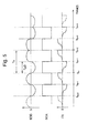
- Fig. 5 examples of the waveforms of the signal SDD and the synchronization clock signal SCK that are generated by the synchronized wave detection part 152 are shown in Fig. 5 and will be described hereinafter. In the following, as shown in Fig. 5 , this will be explained while taking the length of the time interval for 1 bit as the "time interval T B ".
- the binary symbol decoding part 153 described above performs decoding processing of the binary symbol bit data by executing demodulation processing upon the signal SDD, on the basis of the signal SDD and the synchronization clock signal SCK from the synchronized wave detection part 152. It should be understood that it is arranged for the binary symbol decoding part 153, upon receipt of a start command SBC for binary symbol decoding processing from the synchronization control part 159, to start binary symbol decoding processing anew.
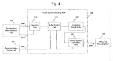
- the binary symbol decoding part 153 having the above function comprises an integration part 210 that serves as an integration means, and a buffer control part 220 that serves as an even/odd detection means and as a specification means. Moreover, this binary symbol decoding part 153 comprises an integration result buffer 230 that serves as a buffer storage means, and a binary symbol calculation part 240 that serves as a calculation means.
- the integration part 210 described above receives the signal SDD and the synchronization clock signal SCK from the synchronized wave detection part 152. And the integration part 210 performs time integration of the signal SDD for each of a front half bit interval, which is the front half of the 1-bit interval, and a rear half bit interval, which is the rear half of the 1-bit interval, thus calculating its integrated values I(t) (where t is time).
- the integration part 210 Having calculated the integrated value I(t 2p+1 ) which is the result of integration over the front half bit interval or the integrated value I(t 2(p+1) ) which is the result of integration over the rear half bit interval, the integration part 210 sends the result of this calculation to the buffer control part 220. It should be understood that it is not arranged for the integration part 210 to recognize whether each of the integration intervals is a front half bit interval or a rear half bit interval; it just performs integration for each half bit interval.
- the values of the signal SDD are positive and negative respectively over almost the entire front half bit interval and over almost the rear half bit interval. Due to this, the positive or negative sign of the integrated value I(t 2p+1 ) which is the result of integration over the front half bit interval, and the positive or negative sign of the integrated value I(t 2(p+1) ) which is the result of integration over the rear half bit interval, are mutually opposite.
- the buffer control part 220 described above upon receipt of the start command SBC from the synchronization control part 159, and after having performed clearing of the integration result buffer 230, the buffer control part 220 described above starts reception of the integration results from the integration part 210. And the buffer control part 220 sequentially stores the integrated values that are reported in the integration result buffer 230 as integration results.
- the buffer control part 220 compares together the positive or negative sign of this new integration result and the positive or negative sign of the integration result that was received directly previously. And, if both of these positive or negative signs are the same, then the occurrence of a phase change in the signal SDD is detected. And it is detected whether the stage of the integration result buffer 230 in which this new integration result is stored is an even numbered stage or an odd numbered stage, and the result of this detection is stored.
- the buffer control part 220 performs this type of detection processing only once, each time it receives the start command SBC from the synchronization control part 159. In other words it is arranged for the buffer control part 220, after receipt of the start command SBC from the synchronization control part 159, to store even/odd information specifying the stage of the integration result buffer 230 in which the integration result at the time point that the phase change was initially detected is stored (hereinafter simply termed "even/odd information"), until it next receives the start command SBC from the synchronization control part 159.
- even/odd information specifying the stage of the integration result buffer 230 in which the integration result at the time point that the phase change was initially detected is stored
- the buffer control part 220 specifies that integration result pairs for 26 symbol bits (each being a pair, related to one symbol bit, of the integration result for its front half bit interval and the integration result for its rear half bit interval) have been stored in the integration result buffer 230, which consists of 52 stages as will be described hereinafter. And, at the time point that this specification has been performed, the buffer control part 220 issues a first calculation command to the binary symbol calculation part 240, to the effect that the data values for these 26 symbol bits are to be calculated. Thereafter, each time two integration results are newly stored in the integration result buffer 230, the buffer control part 220 issues a second calculation command to the effect that the data values for this one symbol bit are to be calculated.
- the binary symbol calculation part 240 described above performs calculation of the data values of the symbol bits.
- the binary symbol calculation part 240 calculates the data value SD r for this symbol bit on the basis of the positive or negative sign of the value SV r .
- it is arranged for the binary symbol calculation part 240 to calculate the data value SD r as being "1" if the value SV r is a positive value, and to calculate the data value SD r as being "0" if the value SV r is a negative value. This way in which this data value SD r is calculated is shown in Fig. 6 .
- the binary symbol calculation part 240 sends the 26 data values SD r that have been calculated to the differential decoding part 154 as the signal BSD, in time order.
- the binary symbol calculation part 240 calculates the data value NSD, in a similar manner to the case for the calculation of the data values SD r . This way in which the data value NSD is calculated is shown in Fig. 7 .
- the binary symbol calculation part 240 sends the data value NSD that has been calculated to the differential decoding part 154 as a signal BSD.
- the differential decoding part 154 described above performs differential decoding upon the data that has arrived from the binary symbol decoding part 153 as the signal BSD. It should be understood that it is arranged for the differential decoding part 154 to perform this differential decoding processing according to the contents of an operation command DDC from the synchronization control part 159. As shown in Fig. 8 , the differential decoding part 154 that has this function comprises a bit data calculation part 260, a bit data buffer 270, and a data output control part 280.
- the bit data calculation part 260 described above receives the signal BSD from the binary symbol decoding part 153. And, when new symbol bit data values as the signal BSD are received, this bit data calculation part 260 compares together the new symbol bit data values and the symbol bit data values that were received as the directly preceding signal BSD, and makes a decision as to whether or not they are the same. And, on the basis of the result of this decision, the bit data calculation part 260 calculates a new information bit data value. Then the bit data calculation part 260 stores the newly calculated data value in the data bit buffer 270. It should be understood that it is arranged for the bit data calculation part 260 to send a storage report to the data output control part 280, each time a newly calculated data value is stored in the data bit buffer 270.
- the bit data buffer 270 described above is a 26-stage bit data buffer, and is made as a so called ring buffer. And it is arranged for data values for the 26 bits that have been sent most recently from the bit data calculation part 260 to be stored in this data bit buffer 270, at a maximum.
- the data output control part 280 In a mode in which it operates according to operating commands DDC from the synchronization control part 159, the data output control part 280 described above reads the data values for 26 bits in the bit data buffer 270, while referring to the storage report from the bit data calculation part 260. And the data output control part 280 sends the data values for these 26 bits that it has read to the error detection/correction part 155 as a signal DDD.
- the error detection/correction part 155 described above performs operation according to an operating command ECC from the synchronization control part 159. If data non-reporting operation is commanded by this operating command ECC, then the error detection/correction part 155 only performs error checking for the data values for 26 bits received from the differential decoding part 154, and sends the checking result EDR to the synchronization control part 159. During this error checking, the error detection/correction part 155 performs syndrome calculation using a generating polynomial equation determined by the RDS format. And the error detection/correction part 155 performs block error checking on the basis of the result of this syndrome calculation.
- This block error checking is performed by checking as to whether or not an offset word has been correctly obtained by the syndrome calculation.
- this checking as to whether an offset word has been correctly obtained or not is performed by checking whether or not one among a plurality of predetermined offset words ("A”, "B", “C”, and "D") has been obtained by the syndrome calculation.
- predetermined offset words the sequence ("A" ⁇ "B” ⁇ "C” ⁇ "D” ⁇ "A” ⁇ ).
- the error detection/correction part 155 when data reporting operation has been commanded as the operating command ECC, in addition to block error checking and checking result reporting, if a block error has been detected, the error detection/correction part 155 also performs correction of the data word on the basis of the result of the syndrome calculation. And, if no block error has been detected, then the error detection/correction part 155 employs the data word just as it is; while, if a block error has been detected, then, while employing the result of correcting the data word, also, each time the data for one new group (the four blocks with offset words from "A" to "D") is complete, the part 155 takes this as a signal RSD, and sends it to the control unit 190.
- PI data and AF data and so on are included in the data sent from the error detection/correction part 155 to the control unit 190.
- the synchronization control part 159 described above controls the operation of the data signal processing unit 150. Upon receipt of a synchronization start command STC from the control unit 190, this synchronization control part 159 starts new synchronization detection control processing. This synchronization control processing by the synchronization control part 159 will be described hereinafter.
- the actuation input unit 160 described above is made as a key part that is provided to a main body portion of the reception device 100, or as a remote input device or the like to which a key part is provided.
- a touch panel that is provided to a display unit not shown in the figures as the key part that is provided to the main body portion.
- the result of actuation input to the actuation input unit 160 is sent to the control unit 190 as actuation input data IPD.
- the audio output unit 170 described above comprises: (i) a DA (Digital to Analogue) converter that converts data received from the stereo demodulation unit 140 to an analog signal; (ii) an amplifier that amplifies this analog signal outputted from the DA converter; and (iii) a speaker that converts the amplified analog signal to audio. It should be understood that (i) through (iii) are provided for each of the L signal LAD and the R signal RAD that are the result of the stereo demodulation processing.
- DA Digital to Analogue
- the control unit 190 described above controls the overall operation of the reception device 100.
- the control unit 190 When the power supply to the reception device 100 is turned ON, the control unit 190 generates a tuning command CSL that commands tuning of a preset broadcasting station, and supplies this command to the tuner unit 120.
- the control unit 190 when a tuning command inputted to the actuation input unit 160 is notified as actuation input data IPD, the control unit 190 generates a tuning command CSL according to this tuning command, and sends this command to the tuner unit 120.
- the control unit 190 generates a tuning command CSL commanding tuning to an optimum broadcasting station that has been obtained by making use of the network follow function in the RDS format, and sends this command to the tuner unit 120.
- the control unit 190 when it sends a tuning command CSL to the tuner unit 120, the control unit 190 then sends the synchronization start command STC to the data signal processing unit 150 (in more detail, to the synchronization control part 159
- control unit 190 performs seek processing for an alternative candidate station and so on.
- synchronization detection processing by the data signal processing unit 150 is started by a synchronization start command STC being sent from the control unit 190 to the data signal processing unit 150.
- a synchronization start command STC being sent from the control unit 190 to the data signal processing unit 150.
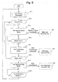
- the synchronization control part 159 in the data signal processing unit 150 first performs initial setting processing in a step S11, as shown in Fig. 9 .
- the synchronization control part 159 performs setting of the error detection/correction part 155 to the data non-reporting mode.
- the synchronization control part 159 establishes this data non-reporting setting by sending a data non-reporting command to the error detection/correction part 155 as the operating command ECC.
- the error detection/correction part 155 performs block error checking and reporting of the results of checking to the synchronization control part 159, only.
- the synchronization control part 159 performs start setting of the binary symbol decoding part 153 for starting binary symbol decoding processing. This start setting for binary symbol decoding processing is performed by the synchronization control part 159 sending the start command SBC to the binary symbol decoding part 153.
- new binary symbol decoding processing is started by the binary symbol decoding part 153.
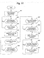
- the buffer control part 220 clears the integration result buffer 230.
- a step S32 the buffer control part 220 makes a decision as to whether or not a new integration result has been acquired from the integration part 210, which performs reporting of an integration result at half-bit intervals, as described above. If the result of this decision is negative (N in the step S32), then the processing of this step S32 is repeated.
- step S33 the buffer control part 220 makes a decision as to whether or not a phase change has occurred in the signal SDD. As described above, the decision as to whether or not such a phase change has occurred is made by the buffer control part 220 comparing together the positive or negative sign of the new integration result and the positive or negative sign of the integration result that was received directly previously.
- step S33 If the result of this decision in the step S33 is negative (N in the step S33), then the flow of control returns to the step S32. And thus the processing of the steps S32 and S33 is repeated, until the occurrence of a phase change is detected.
- step S34 the buffer control part 220 detects whether or not the stage of the integration result buffer 230 in which is stored the integration result that in the step S32 it was decided had been newly acquired, is an even numbered stage. And the buffer control part 220 stores the result of detection as an even/odd detection result.
- the buffer control part 220 makes a decision as to whether or no the integration result buffer 230 has become full.
- the buffer control part 220 performs this decision by making a decision as to whether or not, after execution of the step S31, 52 integration results have been acquired.
- step S35 If the result of the decision in this step S35 is negative (N in the step S35), then the flow of control proceeds to a step S36.
- step S36 the buffer control part 220 makes a decision as to whether or not a new integration result has been acquired from the integration part 210. And if the result of the decision is negative (N in the step S36), then the processing of the step S36 is repeated.
- step S36 When the result of the decision in the step S36 becomes affirmative due to the buffer control part 220 receiving a new integration result from the integration part 210 and storing it in the integration result buffer 230 (Y in the step S36), then the flow of control returns to the step S35. And the processing of the steps S35 and S36 is repeated until the result of the decision in the step S35 becomes affirmative.
- step S37 the buffer control part 220 makes a decision as to whether or no the even/odd detection result that was detected in the previous step S34 is "even". If the result of this decision is negative (N in the step S37), then the integration result for the rear half bit interval is stored in the 0-th stage of the integration result buffer 230, and the flow of control proceeds to a step S38, since there are not integration result pairs for 26 symbol bits stored in the integration result buffer 230.
- the buffer control part 220 makes a decision as to whether or not a new integration result has been acquired from the integration part 210. If the result of this decision is negative (N in the step S38), then the processing of this step S38 is repeated.
- the result of the decision in the step S38 becomes affirmative (Y in the step S38) due to the buffer control part 220 receiving a new integration result from the integration part 210 and storing it in the integration result buffer 230.
- the buffer control part 220 specifies that integration result pairs for 26 symbol bits are stored in the integration result buffer 230. And the flow of control proceeds to a step S39.
- step S37 If the result of the decision in the step S37 described above is affirmative (Y in the step S37), then the integration result for the front half bit interval is stored in the 0-th stage of the integration result buffer 230. Thus, if the result of the decision in the step S38 is affirmative, the buffer control part 220 specifies that integration result pairs for 26 symbol bits are stored in the integration result buffer 230. Then the flow of control proceeds to a step S39.
- the buffer control part 220 which has decided that bit synchronization has been established due to the above specification, sends the first calculation command to the binary symbol calculation part 240, to the effect that the data values for 26 symbol bits are to be calculated. And, upon receipt of this first calculation command, as described above, the binary symbol calculation part 240 reads in the 52 integration results that are stored in the integration result buffer 230, and calculates the data values for these 26 symbol bits. And the binary symbol calculation part 240 sends these data values for the 26 symbol bits that have been calculated to the differential decoding part 154 in order of time.
- a step S40 the buffer control part 220 makes a decision as to whether or not two new integration results have been acquired from the integration part 210. If the result of this decision is negative (N in the step S40), then the processing of this step S40 is repeated.
- the buffer control part 220 specifies that an integration result pair for one new symbol bit is stored in the integration result buffer 230, and the flow of control proceeds to a step S41.
- the buffer control part 220 sends the second calculation command to the binary symbol calculation part 240, to the effect that the data values for one symbol bit are to be calculated. And, upon receipt of this second calculation command, as described above, the binary symbol calculation part 240 reads in the integration results that are stored in the 50-th and the 51-st stages that are stored in the integration result buffer 230, and calculates the data values for this one symbol bit. And the binary symbol calculation part 240 sends these data values for the one symbol bit that have been calculated to the differential decoding part 154.
- the synchronization control part 159 performs setting of the differential decoding part 154 to a first output mode. This setting of the first output mode is performed by the synchronization control part 159 sending a first output command to the differential decoding part 154 as the operating command DDC.
- first output mode processing is started by the differential decoding part 154.
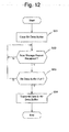
- first output mode processing as shown in Fig. 12 , first in a step S51 the data output control part 280, which has received the first output command, clears the bit data buffer 270.
- the data output control part 280 makes a decision as to whether or not a new storage report has been received from the bit data calculation part 260 that performs bit data calculation as described above and sequentially stores the results of calculation in the bit data buffer 270. If the result of this decision is negative (N in the step S52), then the processing of this step S52 is repeated.
- step S53 the data output control part 280 makes a decision as to whether or no the bit data buffer 270 has become full. This decision is performed by the data output control part 280 making a decision as to whether or not storage reports have been received 26 times after execution of the step S51.
- step S53 If the result of the decision in the step S53 is negative (N in the step S53), the flow of control returns to the step S52. And the processing of the steps S52 and S53 is repeated until the result of the decision in the step S53 becomes affirmative.
- step S54 the data output control part 280 reads in the data values for 26 bits in the bit data buffer 270, and sends them to the error detection/correction part 155. And then the data output control part 280 terminates this first output mode processing.
- the error detection/correction part 155 considers the bit data values for 26 bits that have been received from the differential decoding part 154 as being a block data candidate, and performs block error checking by performing the syndrome calculation described above. And the error detection/correction part 155 sends the result of this checking to the synchronization control part 159.
- step S11 when the first output mode setting described above is completed in the step S23, the processing of the step S11 terminates, and the flow of control proceeds to the step S12 of Fig. 9 .
- the synchronization control part 159 receives the checking result reported from the error detection/correction part 155, and makes a decision as to whether or not a block error has been reported in this checking result.
- step S12 If the result of the decision in the step S12 is affirmative (Y in the step S12), the flow of control proceeds to a step S13.
- step S13 the synchronization control part 159 performs setting of a second output mode to the differential decoding part 154. This second output mode setting is performed by the synchronization control part 159 sending a second output command to the differential decoding part 154 as the operating command DDC.
- second output mode processing is started by the differential decoding part 154.
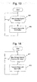
- this second output mode processing as shown in Fig. 13 , first in a step S61 the data output control part 280 makes a decision as to whether or no a new storage report has been received. If the result of this decision is negative (N in the step S61), then the processing of the step S61 is repeated.
- step S61 When the result of the decision in the step S61 becomes affirmative (Y in the step S61) upon receipt of a new storage report from the bit data calculation part 260, the flow of control proceeds to a step S62.
- step S62 the data output control part 280 reads in the data values for 26 bits in the bit data buffer 270, and sends them to the error detection/correction part 155. And then the flow of control returns to the step S61. Subsequently the processing of the steps S61 and S62 is repeated until some output command other than the second output command is received.
- the error detection/correction part 155 each time data values for 26 bits have been received from the differential decoding part 154, the error detection/correction part 155 considers the bit data values for 26 bits that have been received as being a block data candidate, and performs block error checking by performing the syndrome calculation described above. And the error detection/correction part 155 sends the result of this checking to the synchronization control part 159.
- step S 14 each time a checking result has been received by reporting from the error detection/correction part 155, a decision is made as to whether or not a block error has been reported as the checking result. If the result of this decision is affirmative (Y in the step S14), then the processing of the step S14 is repeated.
- step S15 If no block error is reported as the checking result from the error detection/correction part 155 so that the result of the decision in the step S14 becomes negative (N in the step S14), then the flow of control proceeds to a step S 15. Furthermore, the processing also proceeds to this step S 15 if the result of the decision in the step S12 described above is negative (N in the step S12).
- the synchronization control part 159 performs setting to the differential decoding part 154 of a third output mode.
- This third output mode setting is performed by the synchronization control part 159 sending a third output command to the differential decoding part 154 as the operating command DDC.
- third output mode processing is started by the differential decoding part 154.
- the data output control part 280 makes a decision as to whether or no 26 storage reports have newly been received. If the result of this decision is negative (N in the step S71), then the processing of the step S71 is repeated.
- step S71 When the result of the decision in the step S71 becomes affirmative (Y in the step S71) upon receipt of a storage report from the bit data calculation part 260 that storage has been newly performed 26 times, then the flow of control proceeds to a step S72.
- step S72 the data output control part 280 reads in the data values for 26 bits in the bit data buffer 270, and sends them to the error detection/correction part 155. And then the flow of control returns to the step S71. Subsequently the processing of the steps S71 and S72 is repeated until some output command other than the third output command is received.
- the error detection/correction part 155 each time data values for 26 bits have been received from the differential decoding part 154, the error detection/correction part 155 considers the bit data values for 26 bits that have been received as being a block data candidate, and performs block error checking by performing the syndrome calculation described above. And the error detection/correction part 155 sends the result of this checking to the synchronization control part 159.
- a decision is made as to whether or not a checking result has been reported from the error correction/detection part 155 and a block error has been reported as the checking result. If the result of this decision is affirmative (Y in the step S16), the flow of control returns to the step S13. Subsequently the processing of the steps S13 through S16 is repeated, until the result of the decision in this step S16 becomes affirmative.
- step S 17 the synchronization control part 159 establishes a data reporting mode setting for the error detection/correction part 155. This data report setting is performed by the synchronization control part 159 sending a command for data reporting to the error detection/correction part 155 as the operating command ECC.
- the error detection/correction part 155 upon receipt of this data reporting command, the error detection/correction part 155 thereafter, in addition to block error checking and checking result reporting, also, if a block error has been detected, performs correction of the data word on the basis of the results of syndrome calculation. And the error detection part 155 employs the data word just as it is if no block error has been detected, while employing the result of correcting the data word if a block error has been detected, and while also, each time data for a new group is complete, sending this data to the control unit 190 as the signal RSD.
- the RDS data including PI data and AF data and so on is sent to the control unit 190 in this manner after group synchronization has been performed thereupon.
- the synchronization control part 159 makes a decision as to whether or not the preservation of synchronization has been broken.
- this decision is performed by making a decision as to whether or not, in the checking results from the error detection/correction part 155, a block error has been detected for any of a predetermined number of successive data blocks (for example, five).
- step S18 If the result of the decision in this step S18 is negative (N in the step S18), then the processing of the step S18 is repeated. On the other hand, if the result of the decision in the step S18 is affirmative (Y in the step S 18), then the flow of control returns to the step S11, and subsequently the processing of the steps S11 through S18 is repeated.
- control unit 190 Due to data reception processing being performed together with the above synchronization detection processing, data emitted from the broadcasting station to which tuning is set is reported to the control unit 190.
- the control unit 190 performs the control procedure for seeking for alternative candidate stations and so on by utilizing the PI data and AF data and so on included in this type of data.
- stereo demodulation processing is performed by the stereo demodulation unit in parallel with the above described synchronization detection processing. And audio corresponding to the L signal LAD and to the R signal RAD that result from this stereo demodulation processing is reproduced and outputted from the audio output unit 170.
- the buffer control part 220 clears the integration result buffer 230. And next, the buffer control part 220 sequentially stores the results of integration of the binary phase shift keying signal, performed by the integration part 210 for each half bit interval, in the integration result buffer 230.
- the buffer control part 220 detects phase change of the binary phase shift keying signal on the basis of temporal transitions of the values of the integration results. And the buffer control part 220 detects whether the stage of the integration result buffer 230 in which the integration result for the half bit interval directly after the phase change time point is stored is an even numbered stage or an odd numbered stage, and keeps the result of this detection as an even/odd detection result.
- the binary symbol calculation part 240 calculates the data values for these 26 symbol bits on the basis of the 52 integration results stored in the integration result buffer 230. And the results of calculation by the binary symbol calculation part 240 are utilized in the detection of block synchronization.
- block synchronization detection is performed while also utilizing the integration results detected before the phase change of the binary phase shift keying signal.
- it is possible rapidly to perform block synchronization of the data transmitted by the binary phase shift keying signal.
- it is arranged to detect block synchronization when no block data error has been detected in either of two successive block candidates.
- the present invention was applied to a reception device employing the RDS format, it would also be possible to apply the present invention to some format other than the RDS format in which the binary phase modulation format is employed for data transmission, for example to a reception device in which the RBDS (Radio Broadcast Data System) format is employed.
- RDS Radio Broadcast Data System
- the present invention was applied to a FM radio reception device, it would also be possible to apply the present invention to a device that has a function of receiving broadcasts of some other type; and, moreover, it would also be possible to apply the present invention to a broadcast reception device that is mounted to a moving body other than a vehicle. Yet further, for example, it would also be possible to apply the present invention to a device that has a broadcast reception function and that is installed in a household or the like.
- this program could be acquired in a format in which it is recorded upon a transportable recording medium such as a CD-ROM or a DVD or the like; or it could also be acquired in the format of being distributed via a network such as the internet or the like.
Landscapes
- Engineering & Computer Science (AREA)
- Signal Processing (AREA)
- Computer Networks & Wireless Communication (AREA)
- Synchronisation In Digital Transmission Systems (AREA)
Abstract
When synchronization detection processing is started, integration result buffer is cleared. Then, a buffer control part sequentially stores the result of integration of a binary phase shift keying signal for each half bit period that is performed by an integration section in the integration result buffer. The buffer control part detects a phase change of the binary phase shift keying signal according to the temporal change in the value of the integration result. The buffer control part determines whether the stage of the integration result buffer in which the result of the integration for a half bit period just after the time of the phase change is stored is an even or odd stage and confirms that the integration result pair corresponding to 26 symbol bits are stored in the integration result buffer on the basis of the determination. After the confirmation is performed, a binary phase symbol calculation part calculates data values of the 26 symbol bits from 52 integration results stored in the integration result buffer.
Description
- The present invention relates to a block synchronization device, to a reception device, to a block synchronization processing method and a block synchronization processing program, and to a recording medium upon which the block synchronization processing program is recorded.
- From the past, broadcasting in which contents for reproduction consisting of audio and/or images is multiplexed with data has been widespread. As one format for this type of multiplex broadcast, for example, the RDS (Radio Data System) format may be cited, which is much used in Europe. Here, the RDS format is a format in which various types of digital data are transmitted via a FM broadcast signal as multiplexed.
- With this RDS format, program identification code (PI) data for the broadcast that is currently being received, alternative candidate station frequency (AF) list data, and so on are included in the multiplexed data. By using this type of data, it becomes possible to make active use of a network follow function, and to perform processing to seek for an alternative candidate station.
- A data signal that is multiplexed in the RDS format is a binary phase shift keying signal having a predetermined bit rate (1187.5 bps (bits per second)). This signal is carrier wave suppressed amplitude modulated on a subcarrier wave of frequency 57 KHz, which is the third harmonic component of the 19 kHz stereo pilot tone. As a result, it is frequency multiplexed outside the frequency band of the signal wave after FM modulation of the audio signal. It should be understood that, in the RDS format, this data signal is generated by binary phase shift keying of binary symbol data whose information data bit string is created by differential encoding.
- As shown in
Fig. 1 , in this RDS data, one data group DGP consists of four data blocks BLK0 through BLK3. And each of these data blocks BLKj (where j=0 through 3) consists of a 16 bit data word DTWj and a 10 bit check word CKWj. Here, in the RDS format, no common block identification reference symbol is included in the data blocks BLKj (j=0-3). - In processing for receiving such RDS data, block synchronization is performed after having first confirmed bit synchronization. And, when block synchronization has been detected, then group synchronization is performed.
- Here, during block synchronization, for each data block, an offset word that is attached to the
rear half 10 bit check word CKWj is calculated, and block synchronization and group synchronization are checked on the basis of which of certain predetermined values (for example "A", "B", "C", and "D") this offset word that has been calculated is, and on the basis of the periodicity of the offset word that is sequentially calculated (for example "A" → "B" → "C" → "D"). Here, this offset word calculation is performed by syndrome calculation of candidate RDS data blocks (of 26 data bits) according to a predetermined generating polynomial equation (refer toPatent Documents # 1 and #2). - Patent Document #1: Japanese Laid-Open Patent Publication
Heisei 11 (1999)-112478
Patent Document #1: Japanese Laid-Open Patent Publication Heisei8(1996)-79016 - As described above, in the prior art, the operation of checking block synchronization in relation to RDS data is started after having checked bit synchronization. Here, since a signal with RDS data (hereinafter termed an "RDS data signal") is a phase modulated signal, bit synchronization detection is possible due to its phase changing.
- Due to this, in the prior art, the operation of checking for block synchronization in relation to RDS data is performed by employing the RDS data signal after bit synchronization has been detected, in other words after phase changing has been detected. As a result, it has not been possible to anticipate rapid block synchronization.
- Because of this, a technique has been eagerly awaited that can rapidly check block synchronization for RDS data. To respond to this requirement is considered as being one problem that the present invention must solve.
- The present invention has been conceived in consideration of the circumstances described above, and its object is to provide a block synchronization device, a reception device, and a block synchronization processing method, which are capable of rapidly performing block synchronization for data transmitted with a binary phase shift keying signal.
- Considered from a first standpoint, the present invention proposes a block synchronization device that demodulates a binary phase shift keying signal in a continuously synchronous system upon which information data made up from data blocks made up from a predetermined number of data bits is carried, and that performs block synchronization, characterized by comprising: a wave detection means that performs synchronized wave detection upon said binary phase shift keying signal, and generates a wave detection signal and a synchronization clock signal; an integration means that calculates an integrated value of said wave detection signal for each half bit interval, on the basis of said synchronization clock signal; a buffer storage means that sequentially stores just twice said predetermined number of results of integration by said integration means; an even/odd detection means that detects whether the stage of said buffer storage means in which the result of integration of said wave detection signal by said integration means for the half bit interval directly after a phase change time point is stored, is an even numbered stage or an odd numbered stage; a specification means that, on the basis of the result of detection by said even/odd detection means, performs specification that results of integration by said integration means corresponding to said predetermined number of bits are stored in said buffer storage means; and a calculation means that, on the basis of the contents stored in said buffer storage means at the time point that specification is performed by said specification means, calculates data values for each of said predetermined number of bit interval lengths corresponding to the contents stored in said buffer storage means.
- And, considered from a second standpoint, the present invention proposes a reception device that receives a signal upon which is superimposed a binary phase shift keying signal in a continuously synchronous system upon which information data made up from data blocks made up from a predetermined number of data bits is carried, characterized by comprising: a tuning means that performs tuning to a desired broadcasting station that emits a broadcast wave upon which said binary phase shift keying signal is multiplexed; and a block synchronization device as described in any one of
Claims 1 through 5 that demodulates said binary phase shift keying signal and performs block synchronization. - Moreover, considered from a third standpoint, the present invention proposes a block synchronization processing method that is used by a block synchronization device that demodulates a binary phase shift keying signal in a continuously synchronous system upon which information data made up from data blocks made up from a predetermined number of data bits is carried, and that performs block synchronization, characterized by comprising: a wave detection process of performing synchronized wave detection upon said binary phase shift keying signal, and generating a wave detection signal and a synchronization clock signal; an integration process of performing calculation of an integrated value of said wave detection signal for each half bit interval on the basis of said synchronization clock signal, and sequentially storing just twice said predetermined number of results of integration in a buffer storage means; a detection process of detecting whether the stage of said buffer storage means in which the result of integration of said wave detection signal for the half bit interval directly after a phase change time point is stored, is an even numbered stage or an odd numbered stage; a specification process of, on the basis of the result of detection by said detection process, performing specification that results of integration corresponding to said predetermined number of bits are stored in said buffer storage means; and a calculation process of, on the basis of the contents stored in said buffer storage means at the time point that specification is performed by said specification process, calculating data values for each of said predetermined number of bit interval lengths corresponding to the contents stored in said buffer storage means.
- Furthermore, considered from a fourth standpoint, the present invention proposes a block synchronization processing program, characterized in that it causes a calculation means to execute a block synchronization processing method according to the present invention.
- And, considered from a fifth standpoint, the present invention proposes a recording medium, characterized in that a block synchronization processing program according to the present invention is recorded thereupon so as to be readable out by a calculation means.
-
-
Fig. 1 is a figure for explanation of the structure of a data group and data blocks that are employed with the RDS format; -
Fig. 2 is a block diagram of the structure of a reception device according to an embodiment of the present invention; -
Fig. 3 is a block diagram showing the structure of a data signal processing unit ofFig. 2 ; -
Fig. 4 is a block diagram showing the structure of a binary symbol decoding part ofFig. 3 ; -
Fig. 5 is a timing diagram for explanation of the operation of an integration part ofFig. 4 ; -
Fig. 6 is a figure for explanation of symbol calculation operation by a binary symbol decoding calculation part ofFig. 4 (the first part thereof); -
Fig. 7 is a figure for explanation of symbol calculation operation by this binary symbol decoding calculation part ofFig. 4 (the second part thereof); -
Fig. 8 is a block diagram showing the structure of a differential decoding part ofFig. 3 ; -
Fig. 9 is a flow chart for explanation of processing by a synchronization control part ofFig. 3 ; -
Fig. 10 is a flow chart for explanation of initial setting processing inFig. 9 ; -
Fig. 11 is a flow chart for explanation of processing by a buffer control part ofFig. 4 ; -
Fig. 12 is a flow chart for explanation of processing by a data output control part ofFig. 8 (the first part thereof); -
Fig. 13 is a flow chart for explanation of this processing by the data output control part ofFig. 8 (the second part thereof); and -
Fig. 14 is a flow chart for explanation of this processing by the data output control part ofFig. 8 (the third part thereof). - In the following, an embodiment of the present invention will be explained with reference to
Figs. 2 through 14 . It should be understood that, in this embodiment, an example is shown and explained of a FM radio reception device compatible with RDS, which is mounted to a vehicle. Moreover, in the explanation and the drawings, the same reference symbols are affixed to elements that are the same or equivalent, and duplicate explanation is omitted. - The schematic structure of a
reception device 100 according to an embodiment is shown inFig. 2 as a block diagram. As shown in this Fig. 21, thereception device 100 comprises anantenna 110, atuner unit 120 that serves as a tuning means, and a wavewave detection unit 130. Moreover, thereception device 100 comprises astereo demodulation unit 140 and a datasignal processing unit 150 that serves as a block synchronization device. Furthermore, thereception device 100 also comprises anactuation input unit 160, anaudio output unit 170, and acontrol unit 190. - The
antenna 110 described above receives broadcast waves. The result of reception by theantenna 110 is sent to thetuner unit 120 as a signal RFS. - According to a tuning command CSL from the
control unit 190, thetuner unit 120 described above performs tuning processing to extract the signal of the broadcasting station that is to be selected from the signal RFS, and sends it to thewave detection unit 130 as a signal IFD on a predetermined intermediate frequency band. Thistuner unit 120 comprises an input filter, a high frequency amplifier (RF-AMP: Radio Frequency Amplifier), a band pass filter (hereinafter also termed an "RF filter"), a mixer (i.e. a mixing device), an intermediate frequency filter (hereinafter also termed an "IF filter"), an AD (Analogue to Digital) converter (ADC), and a local oscillator circuit, all of which are not shown in the figure. - Here, after the low frequency component in the signal RFS that is received by the
antenna 110 has been eliminated by the input filter, which is a high pass filter, it is amplified by the high frequency amplifier. After a signal in a specific frequency range has been selected with the RF filter, the result of amplification by the high frequency amplifier is sent to the mixer. - In the mixer, the signal that has passed through the RF filter and an oscillation signal corresponding to the tuning command CSL that has been generated by the local oscillation circuit are mixed together. After a signal component in an intermediate frequency range that has been determined in advance has been selected from the signal that results from this mixing by the mixer, it is converted to a digital signal by the ADC. And the result of this conversion is sent to the
wave detection unit 130 as the signal IFD. - The
wave detection unit 130 described above receives the signal IFD from thetuner unit 120. And thewave detection unit 130 performs digital wave detection processing thereupon according to a predetermined method, and generates a signal DSD. The signal DSD that has been generated in this manner is sent to thestereo demodulation unit 140 and to the datasignal processing unit 150. - It should be understood that the signal DSD includes a composite signal component, which is an audio signal, and a RDS data signal component.
- The
stereo demodulation unit 140 described above receives the signal DSD from thewave detection unit 130. First, thisstereo demodulation unit 140 extracts the composite signal included in the signal DSD. And thestereo demodulation unit 140 performs stereo demodulation processing upon this composite signal that it has extracted, and generates a left channel audio signal LAD (hereinafter also termed the "L signal") and a right channel audio signal RAD (hereinafter also termed the "R signal"). The L signal LDA and the R signal RDA that are generated in this manner are outputted to theaudio output unit 170. - The data
signal processing unit 150 described above performs decoding on the basis of the RDS data in the signal DSD from thewave detection unit 130. As shown inFig. 3 , the datasignal processing unit 150 having this function comprises a band pass filter (BPF) 151 and a synchronizedwave detection part 152 that serves as a wave detection means. Moreover, this datasignal processing unit 150 comprises a binarysymbol decoding part 153, adifferential decoding part 154, and an error detection/correction part 155 that serves as an error detection means. Yet further, this datasignal processing unit 150 comprises asynchronization control part 159 that serves as a block synchronization detection means. - The
BPF 151 described above receives the signal DSD from thewave detection unit 130. And theBPF 151 selectively passes through the RDS data signal component in the signal DSD. The signal that has passed through theBPF 151 in this manner is sent to the synchronizedwave detection part 152 as a signal FTD. - The synchronized
wave detection part 152 described above receives the signal FTD from theBPF 151. And this synchronizedwave detection part 152 includes a PLL (Phase Locked Loop) circuit, and, along with performing digital wave detection processing upon the signal FTD and generating a signal SDD which is a binary phase shift keying signal, also generates a synchronization clock signal SCK. The signal SDD and the synchronization clock signal SCK that have been generated in this manner are sent to the binarysymbol decoding part 153. - It should be understood that examples of the waveforms of the signal SDD and the synchronization clock signal SCK that are generated by the synchronized
wave detection part 152 are shown inFig. 5 and will be described hereinafter. In the following, as shown inFig. 5 , this will be explained while taking the length of the time interval for 1 bit as the "time interval TB". - Returning to
Fig. 3 , the binarysymbol decoding part 153 described above performs decoding processing of the binary symbol bit data by executing demodulation processing upon the signal SDD, on the basis of the signal SDD and the synchronization clock signal SCK from the synchronizedwave detection part 152. It should be understood that it is arranged for the binarysymbol decoding part 153, upon receipt of a start command SBC for binary symbol decoding processing from thesynchronization control part 159, to start binary symbol decoding processing anew. - As shown in
Fig. 4 , the binarysymbol decoding part 153 having the above function comprises anintegration part 210 that serves as an integration means, and abuffer control part 220 that serves as an even/odd detection means and as a specification means. Moreover, this binarysymbol decoding part 153 comprises anintegration result buffer 230 that serves as a buffer storage means, and a binarysymbol calculation part 240 that serves as a calculation means. - The
integration part 210 described above receives the signal SDD and the synchronization clock signal SCK from the synchronizedwave detection part 152. And theintegration part 210 performs time integration of the signal SDD for each of a front half bit interval, which is the front half of the 1-bit interval, and a rear half bit interval, which is the rear half of the 1-bit interval, thus calculating its integrated values I(t) (where t is time). - An example of the integrated values I(t) calculated in this manner is shown in
Fig. 5 , along with examples of the waveforms of the signal SDD and the synchronization clock signal SCK described above. It should be understood that, in the following explanation, it will be supposed that the front half bit interval starts directly after the time instant t2p (where p=1, 2, ...), and the rear half bit interval starts directly after the time instant t2p+1 (where p=1, 2, ...). - Having calculated the integrated value I(t2p+1) which is the result of integration over the front half bit interval or the integrated value I(t2(p+1)) which is the result of integration over the rear half bit interval, the
integration part 210 sends the result of this calculation to thebuffer control part 220. It should be understood that it is not arranged for theintegration part 210 to recognize whether each of the integration intervals is a front half bit interval or a rear half bit interval; it just performs integration for each half bit interval. - It should be understood that in this embodiment, as shown in
Fig. 5 , the values of the signal SDD are positive and negative respectively over almost the entire front half bit interval and over almost the rear half bit interval. Due to this, the positive or negative sign of the integrated value I(t2p+1) which is the result of integration over the front half bit interval, and the positive or negative sign of the integrated value I(t2(p+1)) which is the result of integration over the rear half bit interval, are mutually opposite. - Returning to
Fig. 4 , upon receipt of the start command SBC from thesynchronization control part 159, and after having performed clearing of theintegration result buffer 230, thebuffer control part 220 described above starts reception of the integration results from theintegration part 210. And thebuffer control part 220 sequentially stores the integrated values that are reported in theintegration result buffer 230 as integration results. - Furthermore, upon receipt of a new integration result, the
buffer control part 220 compares together the positive or negative sign of this new integration result and the positive or negative sign of the integration result that was received directly previously. And, if both of these positive or negative signs are the same, then the occurrence of a phase change in the signal SDD is detected. And it is detected whether the stage of theintegration result buffer 230 in which this new integration result is stored is an even numbered stage or an odd numbered stage, and the result of this detection is stored. - The
buffer control part 220 performs this type of detection processing only once, each time it receives the start command SBC from thesynchronization control part 159. In other words it is arranged for thebuffer control part 220, after receipt of the start command SBC from thesynchronization control part 159, to store even/odd information specifying the stage of theintegration result buffer 230 in which the integration result at the time point that the phase change was initially detected is stored (hereinafter simply termed "even/odd information"), until it next receives the start command SBC from thesynchronization control part 159. - Moreover, on the basis of the number of integration results that have been received and the even/odd information, the
buffer control part 220 specifies that integration result pairs for 26 symbol bits (each being a pair, related to one symbol bit, of the integration result for its front half bit interval and the integration result for its rear half bit interval) have been stored in theintegration result buffer 230, which consists of 52 stages as will be described hereinafter. And, at the time point that this specification has been performed, thebuffer control part 220 issues a first calculation command to the binarysymbol calculation part 240, to the effect that the data values for these 26 symbol bits are to be calculated. Thereafter, each time two integration results are newly stored in theintegration result buffer 230, thebuffer control part 220 issues a second calculation command to the effect that the data values for this one symbol bit are to be calculated. - The above described
integration result buffer 230 is a data buffer having 52 stages, and is made as a so called ring buffer. Thus, it is arranged for, at a maximum, the 52 integration results most recently sent from thebuffer control part 220 to be stored in thisintegration result buffer 230. It should be understood that the following explanation is expressed in terms of the stage in which the oldest integration result is stored, at each time point, being the 0-th stage, and, in the buffer full state, in terms of the newest integration result being stored in the 51-st stage. Furthermore, it will be supposed that the integration result stored in the q-th stage (where q=0, 1, ... 51) is the "integration result IRq". - Upon a calculation command from the
buffer control part 220, the binarysymbol calculation part 240 described above performs calculation of the data values of the symbol bits. Here, when the first calculation command is received as this calculation command, the 52 integration results that are stored in theintegration result buffer 230 are read in, and data values SDr (where r=0 to 25) are calculated for their 26 symbol bits. - During the calculation of each of these data values SDr (="0" or "1"), in this embodiment, the binary
symbol calculation part 240 first calculates a value SVr according to the following Equation (1):
- Next, the binary
symbol calculation part 240 calculates the data value SDr for this symbol bit on the basis of the positive or negative sign of the value SVr. In this embodiment, it is arranged for the binarysymbol calculation part 240 to calculate the data value SDr as being "1" if the value SVr is a positive value, and to calculate the data value SDr as being "0" if the value SVr is a negative value. This way in which this data value SDr is calculated is shown inFig. 6 . - And the binary
symbol calculation part 240 sends the 26 data values SDr that have been calculated to thedifferential decoding part 154 as the signal BSD, in time order. - Moreover, upon receipt of the second calculation command from the
buffer control part 220 as the calculation command, the binarysymbol calculation part 240 reads in the integration results IR50 and IR51 that are stored in theintegration result buffer 230, and calculates a data value NSD of one symbol bit. During the calculation of this data value NSD, in this embodiment, the binarysymbol calculation part 240 first calculates a value NSV according to the following Equation (2):
- Next, on the basis of the positive or negative sign of the value NSV, the binary
symbol calculation part 240 calculates the data value NSD, in a similar manner to the case for the calculation of the data values SDr. This way in which the data value NSD is calculated is shown inFig. 7 . - And the binary
symbol calculation part 240 sends the data value NSD that has been calculated to thedifferential decoding part 154 as a signal BSD. - Returning to
Fig. 3 , thedifferential decoding part 154 described above performs differential decoding upon the data that has arrived from the binarysymbol decoding part 153 as the signal BSD. It should be understood that it is arranged for thedifferential decoding part 154 to perform this differential decoding processing according to the contents of an operation command DDC from thesynchronization control part 159. As shown inFig. 8 , thedifferential decoding part 154 that has this function comprises a bitdata calculation part 260, abit data buffer 270, and a dataoutput control part 280. - The bit
data calculation part 260 described above receives the signal BSD from the binarysymbol decoding part 153. And, when new symbol bit data values as the signal BSD are received, this bitdata calculation part 260 compares together the new symbol bit data values and the symbol bit data values that were received as the directly preceding signal BSD, and makes a decision as to whether or not they are the same. And, on the basis of the result of this decision, the bitdata calculation part 260 calculates a new information bit data value. Then the bitdata calculation part 260 stores the newly calculated data value in the data bitbuffer 270. It should be understood that it is arranged for the bitdata calculation part 260 to send a storage report to the dataoutput control part 280, each time a newly calculated data value is stored in the data bitbuffer 270. - In this embodiment, it is arranged for "0" to be calculated as the data value of the new information bit if the result of the decision described above is affirmative. Moreover, it is arranged for "1" to be calculated as the data value of the new information bit if the result of the decision described above is negative.
- The
bit data buffer 270 described above is a 26-stage bit data buffer, and is made as a so called ring buffer. And it is arranged for data values for the 26 bits that have been sent most recently from the bitdata calculation part 260 to be stored in this data bitbuffer 270, at a maximum. - In a mode in which it operates according to operating commands DDC from the
synchronization control part 159, the dataoutput control part 280 described above reads the data values for 26 bits in thebit data buffer 270, while referring to the storage report from the bitdata calculation part 260. And the dataoutput control part 280 sends the data values for these 26 bits that it has read to the error detection/correction part 155 as a signal DDD. - It should be understood that, while first through third output commands are issued with the operating command DDC, the operation of the data
output control part 280 corresponding to these output commands will be described hereinafter. - Returning to
Fig. 3 , the error detection/correction part 155 described above performs operation according to an operating command ECC from thesynchronization control part 159. If data non-reporting operation is commanded by this operating command ECC, then the error detection/correction part 155 only performs error checking for the data values for 26 bits received from thedifferential decoding part 154, and sends the checking result EDR to thesynchronization control part 159. During this error checking, the error detection/correction part 155 performs syndrome calculation using a generating polynomial equation determined by the RDS format. And the error detection/correction part 155 performs block error checking on the basis of the result of this syndrome calculation. - This block error checking is performed by checking as to whether or not an offset word has been correctly obtained by the syndrome calculation. Here, for the first block error check after synchronization detection operation starts, this checking as to whether an offset word has been correctly obtained or not is performed by checking whether or not one among a plurality of predetermined offset words ("A", "B", "C", and "D") has been obtained by the syndrome calculation. And, for subsequent block error checks, furthermore, it is performed by checking whether or not the offset word that has been obtained by the syndrome calculation is obtained according to a predetermined sequence (the sequence ("A" → "B"→ "C"→ "D"→ "A" →...).
- Furthermore, when data reporting operation has been commanded as the operating command ECC, in addition to block error checking and checking result reporting, if a block error has been detected, the error detection/
correction part 155 also performs correction of the data word on the basis of the result of the syndrome calculation. And, if no block error has been detected, then the error detection/correction part 155 employs the data word just as it is; while, if a block error has been detected, then, while employing the result of correcting the data word, also, each time the data for one new group (the four blocks with offset words from "A" to "D") is complete, thepart 155 takes this as a signal RSD, and sends it to thecontrol unit 190. - It should be understood that PI data and AF data and so on are included in the data sent from the error detection/
correction part 155 to thecontrol unit 190. - The
synchronization control part 159 described above controls the operation of the datasignal processing unit 150. Upon receipt of a synchronization start command STC from thecontrol unit 190, thissynchronization control part 159 starts new synchronization detection control processing. This synchronization control processing by thesynchronization control part 159 will be described hereinafter. - Returning to
Fig. 2 , theactuation input unit 160 described above is made as a key part that is provided to a main body portion of thereception device 100, or as a remote input device or the like to which a key part is provided. Here, it is possible to use a touch panel that is provided to a display unit not shown in the figures as the key part that is provided to the main body portion. Moreover, instead of providing a key part, it would also be acceptable to employ a structure for audio input. The result of actuation input to theactuation input unit 160 is sent to thecontrol unit 190 as actuation input data IPD. - The
audio output unit 170 described above comprises: (i) a DA (Digital to Analogue) converter that converts data received from thestereo demodulation unit 140 to an analog signal; (ii) an amplifier that amplifies this analog signal outputted from the DA converter; and (iii) a speaker that converts the amplified analog signal to audio. It should be understood that (i) through (iii) are provided for each of the L signal LAD and the R signal RAD that are the result of the stereo demodulation processing. - The
control unit 190 described above controls the overall operation of thereception device 100. When the power supply to thereception device 100 is turned ON, thecontrol unit 190 generates a tuning command CSL that commands tuning of a preset broadcasting station, and supplies this command to thetuner unit 120. Moreover, when a tuning command inputted to theactuation input unit 160 is notified as actuation input data IPD, thecontrol unit 190 generates a tuning command CSL according to this tuning command, and sends this command to thetuner unit 120. Furthermore, thecontrol unit 190 generates a tuning command CSL commanding tuning to an optimum broadcasting station that has been obtained by making use of the network follow function in the RDS format, and sends this command to thetuner unit 120. And, when it sends a tuning command CSL to thetuner unit 120, thecontrol unit 190 then sends the synchronization start command STC to the data signal processing unit 150 (in more detail, to the synchronization control part 159). - Furthermore, on the basis of the PI data and the AF data and so on included in the signal RSD from the data
signal processing unit 150, thecontrol unit 190 performs seek processing for an alternative candidate station and so on. - Next the operation of the
reception device 100 having the structure described above will be explained, with attention being principally directed to the processing performed by thesynchronization control part 159, by thebuffer control part 220, and by the dataoutput control part 280 in the synchronization detection processing by the datasignal processing unit 150. - After a tuning command CSL has been sent from the
control unit 190 to thetuner unit 120 that corresponds to the preset broadcasting station, to a broadcasting station designated by the user, or to an optimum broadcasting station, synchronization detection processing by the datasignal processing unit 150 is started by a synchronization start command STC being sent from thecontrol unit 190 to the datasignal processing unit 150. During this synchronization detection processing, upon receipt of the synchronization start command STC, thesynchronization control part 159 in the datasignal processing unit 150 first performs initial setting processing in a step S11, as shown inFig. 9 . - During this initial setting processing, as shown in
Fig. 10 , first in a step S21 thesynchronization control part 159 performs setting of the error detection/correction part 155 to the data non-reporting mode. Thesynchronization control part 159 establishes this data non-reporting setting by sending a data non-reporting command to the error detection/correction part 155 as the operating command ECC. Upon receipt of this data non-reporting command, subsequently, the error detection/correction part 155 performs block error checking and reporting of the results of checking to thesynchronization control part 159, only. - Next, in a step S22, the
synchronization control part 159 performs start setting of the binarysymbol decoding part 153 for starting binary symbol decoding processing. This start setting for binary symbol decoding processing is performed by thesynchronization control part 159 sending the start command SBC to the binarysymbol decoding part 153. - Upon receipt of this start command SBC, new binary symbol decoding processing is started by the binary
symbol decoding part 153. As shown inFig. 11 , in this binary symbol decoding processing, first in a step S31, upon receipt of the start command SBC, thebuffer control part 220 clears theintegration result buffer 230. - Next in a step S32 the
buffer control part 220 makes a decision as to whether or not a new integration result has been acquired from theintegration part 210, which performs reporting of an integration result at half-bit intervals, as described above. If the result of this decision is negative (N in the step S32), then the processing of this step S32 is repeated. - But when the result of this decision is affirmative (Y in the step S32) due to the
buffer control part 220 receiving a new integration result from theintegration part 210 and storing it in theintegration result buffer 230, then the flow of control proceeds to a step S33. In this step S33, thebuffer control part 220 makes a decision as to whether or not a phase change has occurred in the signal SDD. As described above, the decision as to whether or not such a phase change has occurred is made by thebuffer control part 220 comparing together the positive or negative sign of the new integration result and the positive or negative sign of the integration result that was received directly previously. - If the result of this decision in the step S33 is negative (N in the step S33), then the flow of control returns to the step S32. And thus the processing of the steps S32 and S33 is repeated, until the occurrence of a phase change is detected.
- But when the result of this decision in the step S33 is positive (Y in the step S33), then the flow of control proceeds to a step S34. In this step S34, the
buffer control part 220 detects whether or not the stage of theintegration result buffer 230 in which is stored the integration result that in the step S32 it was decided had been newly acquired, is an even numbered stage. And thebuffer control part 220 stores the result of detection as an even/odd detection result. - Next, in a step S35, the
buffer control part 220 makes a decision as to whether or no theintegration result buffer 230 has become full. Thebuffer control part 220 performs this decision by making a decision as to whether or not, after execution of the step S31, 52 integration results have been acquired. - If the result of the decision in this step S35 is negative (N in the step S35), then the flow of control proceeds to a step S36. In this step S36, the
buffer control part 220 makes a decision as to whether or not a new integration result has been acquired from theintegration part 210. And if the result of the decision is negative (N in the step S36), then the processing of the step S36 is repeated. - When the result of the decision in the step S36 becomes affirmative due to the
buffer control part 220 receiving a new integration result from theintegration part 210 and storing it in the integration result buffer 230 (Y in the step S36), then the flow of control returns to the step S35. And the processing of the steps S35 and S36 is repeated until the result of the decision in the step S35 becomes affirmative. - When, after the execution of the step S31, the result of the decision in the step S35 becomes affirmative due to the
buffer control part 220 acquiring 52 integration results (Y in the step S35), then the flow of control proceeds to a step S37. In this step S37, thebuffer control part 220 makes a decision as to whether or no the even/odd detection result that was detected in the previous step S34 is "even". If the result of this decision is negative (N in the step S37), then the integration result for the rear half bit interval is stored in the 0-th stage of theintegration result buffer 230, and the flow of control proceeds to a step S38, since there are not integration result pairs for 26 symbol bits stored in theintegration result buffer 230. - In this step S38, the
buffer control part 220 makes a decision as to whether or not a new integration result has been acquired from theintegration part 210. If the result of this decision is negative (N in the step S38), then the processing of this step S38 is repeated. - The result of the decision in the step S38 becomes affirmative (Y in the step S38) due to the
buffer control part 220 receiving a new integration result from theintegration part 210 and storing it in theintegration result buffer 230. When the result of the decision in the step S38 becomes affirmative in this manner, then thebuffer control part 220 specifies that integration result pairs for 26 symbol bits are stored in theintegration result buffer 230. And the flow of control proceeds to a step S39. - If the result of the decision in the step S37 described above is affirmative (Y in the step S37), then the integration result for the front half bit interval is stored in the 0-th stage of the
integration result buffer 230. Thus, if the result of the decision in the step S38 is affirmative, thebuffer control part 220 specifies that integration result pairs for 26 symbol bits are stored in theintegration result buffer 230. Then the flow of control proceeds to a step S39. - Bit synchronization is performed by this type of specification.
- In the step S39 the
buffer control part 220, which has decided that bit synchronization has been established due to the above specification, sends the first calculation command to the binarysymbol calculation part 240, to the effect that the data values for 26 symbol bits are to be calculated. And, upon receipt of this first calculation command, as described above, the binarysymbol calculation part 240 reads in the 52 integration results that are stored in theintegration result buffer 230, and calculates the data values for these 26 symbol bits. And the binarysymbol calculation part 240 sends these data values for the 26 symbol bits that have been calculated to thedifferential decoding part 154 in order of time. - When the issuing of the first calculation command in the step S39 described above has been completed, in a step S40, the
buffer control part 220 makes a decision as to whether or not two new integration results have been acquired from theintegration part 210. If the result of this decision is negative (N in the step S40), then the processing of this step S40 is repeated. - However, when the result of the decision in the step S40 is affirmative (Y in the step S40) due to the
buffer control part 220 receiving two new integration results in sequence from theintegration part 210 and storing them in theintegration result buffer 230, then thebuffer control part 220 specifies that an integration result pair for one new symbol bit is stored in theintegration result buffer 230, and the flow of control proceeds to a step S41. - In this step S41, the
buffer control part 220 sends the second calculation command to the binarysymbol calculation part 240, to the effect that the data values for one symbol bit are to be calculated. And, upon receipt of this second calculation command, as described above, the binarysymbol calculation part 240 reads in the integration results that are stored in the 50-th and the 51-st stages that are stored in theintegration result buffer 230, and calculates the data values for this one symbol bit. And the binarysymbol calculation part 240 sends these data values for the one symbol bit that have been calculated to thedifferential decoding part 154. - Subsequently, the processing of the steps S40 and S41 is repeated until a new start command SBC is received.
- Returning to
Fig. 10 , when the start setting for binary symbol decoding processing in the step S22 has been completed, in a step S23, thesynchronization control part 159 performs setting of thedifferential decoding part 154 to a first output mode. This setting of the first output mode is performed by thesynchronization control part 159 sending a first output command to thedifferential decoding part 154 as the operating command DDC. - Upon receipt of this first output command, first output mode processing is started by the
differential decoding part 154. In this first output mode processing, as shown inFig. 12 , first in a step S51 the dataoutput control part 280, which has received the first output command, clears thebit data buffer 270. - Next, in a step S52, the data
output control part 280 makes a decision as to whether or not a new storage report has been received from the bitdata calculation part 260 that performs bit data calculation as described above and sequentially stores the results of calculation in thebit data buffer 270. If the result of this decision is negative (N in the step S52), then the processing of this step S52 is repeated. - When a new storage report is received from the bit
data calculation part 260 and the result of the decision in the step S52 becomes affirmative (Y in the step S52), the flow of control proceeds to a step S53. In this step S53, the dataoutput control part 280 makes a decision as to whether or no thebit data buffer 270 has become full. This decision is performed by the dataoutput control part 280 making a decision as to whether or not storage reports have been received 26 times after execution of the step S51. - If the result of the decision in the step S53 is negative (N in the step S53), the flow of control returns to the step S52. And the processing of the steps S52 and S53 is repeated until the result of the decision in the step S53 becomes affirmative.
- When the
bit data buffer 270 becomes full and the result of the decision in the step S53 becomes affirmative (Y in the step S53), the flow of control proceeds to a step S54. In this step S54, the dataoutput control part 280 reads in the data values for 26 bits in thebit data buffer 270, and sends them to the error detection/correction part 155. And then the dataoutput control part 280 terminates this first output mode processing. - It should be understood that the error detection/
correction part 155 considers the bit data values for 26 bits that have been received from thedifferential decoding part 154 as being a block data candidate, and performs block error checking by performing the syndrome calculation described above. And the error detection/correction part 155 sends the result of this checking to thesynchronization control part 159. - Returning to
Fig. 10 , when the first output mode setting described above is completed in the step S23, the processing of the step S11 terminates, and the flow of control proceeds to the step S12 ofFig. 9 . In this step S12, thesynchronization control part 159 receives the checking result reported from the error detection/correction part 155, and makes a decision as to whether or not a block error has been reported in this checking result. - If the result of the decision in the step S12 is affirmative (Y in the step S12), the flow of control proceeds to a step S13. In this step S13, the
synchronization control part 159 performs setting of a second output mode to thedifferential decoding part 154. This second output mode setting is performed by thesynchronization control part 159 sending a second output command to thedifferential decoding part 154 as the operating command DDC. - Upon receipt of the second output command, second output mode processing is started by the
differential decoding part 154. In this second output mode processing, as shown inFig. 13 , first in a step S61 the dataoutput control part 280 makes a decision as to whether or no a new storage report has been received. If the result of this decision is negative (N in the step S61), then the processing of the step S61 is repeated. - When the result of the decision in the step S61 becomes affirmative (Y in the step S61) upon receipt of a new storage report from the bit
data calculation part 260, the flow of control proceeds to a step S62. In this step S62, the dataoutput control part 280 reads in the data values for 26 bits in thebit data buffer 270, and sends them to the error detection/correction part 155. And then the flow of control returns to the step S61. Subsequently the processing of the steps S61 and S62 is repeated until some output command other than the second output command is received. - It should be understood that, each time data values for 26 bits have been received from the
differential decoding part 154, the error detection/correction part 155 considers the bit data values for 26 bits that have been received as being a block data candidate, and performs block error checking by performing the syndrome calculation described above. And the error detection/correction part 155 sends the result of this checking to thesynchronization control part 159. - Returning to
Fig. 9 , when the second output mode setting in the step S 13 described above has been completed, in astep S 14, each time a checking result has been received by reporting from the error detection/correction part 155, a decision is made as to whether or not a block error has been reported as the checking result. If the result of this decision is affirmative (Y in the step S14), then the processing of the step S14 is repeated. - If no block error is reported as the checking result from the error detection/
correction part 155 so that the result of the decision in the step S14 becomes negative (N in the step S14), then the flow of control proceeds to astep S 15. Furthermore, the processing also proceeds to this step S 15 if the result of the decision in the step S12 described above is negative (N in the step S12). - In this step S15, the
synchronization control part 159 performs setting to thedifferential decoding part 154 of a third output mode. This third output mode setting is performed by thesynchronization control part 159 sending a third output command to thedifferential decoding part 154 as the operating command DDC. - Upon receipt of the third output command, third output mode processing is started by the
differential decoding part 154. In this third output mode processing, as shown inFig. 14 , first in a step S71 the dataoutput control part 280 makes a decision as to whether or no 26 storage reports have newly been received. If the result of this decision is negative (N in the step S71), then the processing of the step S71 is repeated. - When the result of the decision in the step S71 becomes affirmative (Y in the step S71) upon receipt of a storage report from the bit
data calculation part 260 that storage has been newly performed 26 times, then the flow of control proceeds to a step S72. In this step S72, the dataoutput control part 280 reads in the data values for 26 bits in thebit data buffer 270, and sends them to the error detection/correction part 155. And then the flow of control returns to the step S71. Subsequently the processing of the steps S71 and S72 is repeated until some output command other than the third output command is received. - It should be understood that, each time data values for 26 bits have been received from the
differential decoding part 154, the error detection/correction part 155 considers the bit data values for 26 bits that have been received as being a block data candidate, and performs block error checking by performing the syndrome calculation described above. And the error detection/correction part 155 sends the result of this checking to thesynchronization control part 159. - Returning to
Fig. 9 , when the third output mode setting in the step S15 described above has been completed, in a step S16, a decision is made as to whether or not a checking result has been reported from the error correction/detection part 155 and a block error has been reported as the checking result. If the result of this decision is affirmative (Y in the step S16), the flow of control returns to the step S13. Subsequently the processing of the steps S13 through S16 is repeated, until the result of the decision in this step S16 becomes affirmative. - If the result of the decision in the step S16 is negative (N in the step S16), then it is decided that block synchronization has been performed if a block data error is not detected for either of the two succeeding block candidates, and the flow of control proceeds to a
step S 17 . In this step S 17, thesynchronization control part 159 establishes a data reporting mode setting for the error detection/correction part 155. This data report setting is performed by thesynchronization control part 159 sending a command for data reporting to the error detection/correction part 155 as the operating command ECC. - And, upon receipt of this data reporting command, the error detection/
correction part 155 thereafter, in addition to block error checking and checking result reporting, also, if a block error has been detected, performs correction of the data word on the basis of the results of syndrome calculation. And theerror detection part 155 employs the data word just as it is if no block error has been detected, while employing the result of correcting the data word if a block error has been detected, and while also, each time data for a new group is complete, sending this data to thecontrol unit 190 as the signal RSD. The RDS data including PI data and AF data and so on is sent to thecontrol unit 190 in this manner after group synchronization has been performed thereupon. - Next, in a step S18, the
synchronization control part 159 makes a decision as to whether or not the preservation of synchronization has been broken. In this embodiment, this decision is performed by making a decision as to whether or not, in the checking results from the error detection/correction part 155, a block error has been detected for any of a predetermined number of successive data blocks (for example, five). - If the result of the decision in this step S18 is negative (N in the step S18), then the processing of the step S18 is repeated. On the other hand, if the result of the decision in the step S18 is affirmative (Y in the step S 18), then the flow of control returns to the step S11, and subsequently the processing of the steps S11 through S18 is repeated.
- Due to data reception processing being performed together with the above synchronization detection processing, data emitted from the broadcasting station to which tuning is set is reported to the
control unit 190. Thecontrol unit 190 performs the control procedure for seeking for alternative candidate stations and so on by utilizing the PI data and AF data and so on included in this type of data. - Moreover, in this
reception device 100, stereo demodulation processing is performed by the stereo demodulation unit in parallel with the above described synchronization detection processing. And audio corresponding to the L signal LAD and to the R signal RAD that result from this stereo demodulation processing is reproduced and outputted from theaudio output unit 170. - As has been explained above, in this embodiment, when the synchronization detection processing is started, first, the
buffer control part 220 clears theintegration result buffer 230. And next, thebuffer control part 220 sequentially stores the results of integration of the binary phase shift keying signal, performed by theintegration part 210 for each half bit interval, in theintegration result buffer 230. - When storing this type of integration results in the
integration result buffer 230, thebuffer control part 220 detects phase change of the binary phase shift keying signal on the basis of temporal transitions of the values of the integration results. And thebuffer control part 220 detects whether the stage of theintegration result buffer 230 in which the integration result for the half bit interval directly after the phase change time point is stored is an even numbered stage or an odd numbered stage, and keeps the result of this detection as an even/odd detection result. - Subsequently when, on the basis of these even/odd detection results, it is specified by the
buffer control part 220 that integration result pairs corresponding to 26 symbol bits have been stored in theintegration result buffer 230, then the binarysymbol calculation part 240 calculates the data values for these 26 symbol bits on the basis of the 52 integration results stored in theintegration result buffer 230. And the results of calculation by the binarysymbol calculation part 240 are utilized in the detection of block synchronization. - Due to this, block synchronization detection is performed while also utilizing the integration results detected before the phase change of the binary phase shift keying signal. Thus, according to this embodiment, it is possible rapidly to perform block synchronization of the data transmitted by the binary phase shift keying signal.
- The present invention is not to be considered as being limited to the embodiment described above; alterations of various types are possible.
- For example, in the embodiment described above, it is arranged to detect block synchronization when no block data error has been detected in either of two successive block candidates. By contrast, it would also be acceptable to arrange to detect block synchronization when no block data error has been detected in any of three successive block candidates. Furthermore, it would also be acceptable to arrange to detect block synchronization when no block data error has been detected in some predetermined number of block candidates, among three or more successive block candidates.
- Furthermore, in the embodiment described above, an example was disclosed in which it was detected that block synchronization had been broken if block data errors were detected for each of five successive block candidates. By contrast, it would also be acceptable to arrange to detect that block synchronization has been broken if block data errors are detected for each of a plurality of block candidates other than five.
- Moreover while , in the embodiment described above, the present invention was applied to a reception device employing the RDS format, it would also be possible to apply the present invention to some format other than the RDS format in which the binary phase modulation format is employed for data transmission, for example to a reception device in which the RBDS (Radio Broadcast Data System) format is employed.
- Moreover while , in the embodiment described above, the present invention was applied to a FM radio reception device, it would also be possible to apply the present invention to a device that has a function of receiving broadcasts of some other type; and, moreover, it would also be possible to apply the present invention to a broadcast reception device that is mounted to a moving body other than a vehicle. Yet further, for example, it would also be possible to apply the present invention to a device that has a broadcast reception function and that is installed in a household or the like.
- It should be understood that it would also be acceptable to arrange for parts or all of the
wave detection unit 130, thestereo demodulation unit 140, the datasignal processing unit 150, and thecontrol unit 190 of the embodiment described above to be constituted by a computer that serves as a calculation means and that has a central processing device (CPU: Central Processing Unit), a read only memory (ROM: Read Only Memory), a random access memory (RAM: Random Access Memory) and so on, and to arrange to perform all or parts of the processing of the embodiment described above by executing a program that has been prepared in advance upon the computer. It would be acceptable to arrange for this program to be acquired in a format in which it is recorded upon a transportable recording medium such as a CD-ROM or a DVD or the like; or it could also be acquired in the format of being distributed via a network such as the internet or the like.
Claims (10)
- A block synchronization device that demodulates a binary phase shift keying signal in a continuously synchronous system upon which information data made up from data blocks made up from a predetermined number of data bits is carried, and that performs block synchronization, characterized by comprising:a wave detection means that performs synchronized wave detection upon said binary phase shift keying signal, and generates a wave detection signal and a synchronization clock signal;an integration means that calculates an integrated value of said wave detection signal for each half bit interval, on the basis of said synchronization clock signal;a buffer storage means that sequentially stores just twice said predetermined number of results of integration by said integration means;an even/odd detection means that detects whether the stage of said buffer storage means in which the result of integration of said wave detection signal by said integration means for the half bit interval directly after a phase change time point is stored, is an even numbered stage or an odd numbered stage;a specification means that, on the basis of the result of detection by said even/odd detection means, performs specification that results of integration by said integration means corresponding to said predetermined number of bits are stored in said buffer storage means; anda calculation means that, on the basis of the contents stored in said buffer storage means at the time point that specification is performed by said specification means, calculates data values for each of said predetermined number of bit interval lengths corresponding to the contents stored in said buffer storage means.
- A block synchronization device according to Claim 1, characterized in that:for each of said half bit intervals, over almost its entire extent, the signal value of said wave detection signal is one of positive and negative; andsaid calculation means:for two integration results that correspond to one bit, inverts the sign of a predetermined one of those integration results as determined by the sequence of integration time points, and adds it to the other of those integration results; andobtains a digital value corresponding to each bit, on the basis of the sign of the value that is the result of said addition.
- A block synchronization device according to Claim 1 or Claim 2, characterized by further comprising:an error detection means that, for said predetermined number of bit data items of said information data obtained from the result of calculation by said calculation means, performs detection of a block data error according to a block data error detection method determined for said data block; anda block synchronization detection means that performs block synchronization detection on the basis of temporal transitions of the result of block data error detection by said error detection means.
- A block synchronization device according to Claim 3, characterized in that said block synchronization detection means decides that said block synchronization has been performed, if no block data error has been detected by said error detection means for any one of a first predetermined block number of successive block candidates.
- A block synchronization device according to Claim 3, characterized in that said block synchronization detection means decides that said block synchronization has been performed, if among a first predetermined block number of successive block candidates, a block data error has not been detected by said error detection means for a second predetermined block number of block candidates.
- A reception device that receives a signal upon which is superimposed a binary phase shift keying signal in a continuously synchronous system upon which information data made up from data blocks made up from a predetermined number of data bits is carried, characterized by comprising:a tuning means that performs tuning to a desired broadcasting station that emits a broadcast wave upon which said binary phase shift keying signal is multiplexed; anda block synchronization device as described in any one of Claims 1 through 5 that demodulates said binary phase shift keying signal and performs block synchronization.
- A reception device according to Claim 6, characterized being a radio data system reception device.
- A block synchronization processing method that is used by a block synchronization device that demodulates a binary phase shift keying signal in a continuously synchronous system upon which information data made up from data blocks made up from a predetermined number of data bits is carried, and that performs block synchronization, characterized by comprising:a wave detection process of performing synchronized wave detection upon said binary phase shift keying signal, and generating a wave detection signal and a synchronization clock signal;an integration process of performing calculation of an integrated value of said wave detection signal for each half bit interval on the basis of said synchronization clock signal, and sequentially storing just twice said predetermined number of results of integration in a buffer storage means;a detection process of detecting whether the stage of said buffer storage means in which the result of integration of said wave detection signal for the half bit interval directly after a phase change time point is stored, is an even numbered stage or an odd numbered stage;a specification process of, on the basis of the result of detection by said detection process, performing specification that results of integration corresponding to said predetermined number of bits are stored in said buffer storage means; anda calculation process of, on the basis of the contents stored in said buffer storage means at the time point that specification is performed by said specification process, calculating data values for each of said predetermined number of bit interval lengths corresponding to the contents stored in said buffer storage means.
- A block synchronization processing program, characterized in that it causes a calculation means to execute a block synchronization processing method according to Claim 8.
- A recording medium, characterized in that a block synchronization processing program according to Claim 9 is recorded thereupon so as to be readable out by a calculation means.
Applications Claiming Priority (1)
| Application Number | Priority Date | Filing Date | Title |
|---|---|---|---|
| PCT/JP2008/073574 WO2010073335A1 (en) | 2008-12-25 | 2008-12-25 | Block synchronization device, reception device, and block synchronization processing method |
Publications (1)
| Publication Number | Publication Date |
|---|---|
| EP2372942A1 true EP2372942A1 (en) | 2011-10-05 |
Family
ID=42287004
Family Applications (1)
| Application Number | Title | Priority Date | Filing Date |
|---|---|---|---|
| EP08879131A Withdrawn EP2372942A1 (en) | 2008-12-25 | 2008-12-25 | Block synchronization device, reception device, and block synchronization processing method |
Country Status (2)
| Country | Link |
|---|---|
| EP (1) | EP2372942A1 (en) |
| WO (1) | WO2010073335A1 (en) |
Cited By (1)
| Publication number | Priority date | Publication date | Assignee | Title |
|---|---|---|---|---|
| FR3050347A1 (en) * | 2016-04-18 | 2017-10-20 | Continental Automotive France | DECODER RDS |
Family Cites Families (3)
| Publication number | Priority date | Publication date | Assignee | Title |
|---|---|---|---|---|
| JP3320915B2 (en) | 1994-09-07 | 2002-09-03 | パイオニア株式会社 | Network follow processing method and RDS receiver executing the same |
| JP3416487B2 (en) | 1997-09-29 | 2003-06-16 | 三洋電機株式会社 | FM multiplex signal demodulator |
| JP2002281008A (en) * | 2001-03-21 | 2002-09-27 | Hitachi Kokusai Electric Inc | Bit synchronization detection method |
-
2008
- 2008-12-25 EP EP08879131A patent/EP2372942A1/en not_active Withdrawn
- 2008-12-25 WO PCT/JP2008/073574 patent/WO2010073335A1/en not_active Ceased
Non-Patent Citations (1)
| Title |
|---|
| See references of WO2010073335A1 * |
Cited By (3)
| Publication number | Priority date | Publication date | Assignee | Title |
|---|---|---|---|---|
| FR3050347A1 (en) * | 2016-04-18 | 2017-10-20 | Continental Automotive France | DECODER RDS |
| WO2017182750A1 (en) * | 2016-04-18 | 2017-10-26 | Continental Automotive France | Rds decoder |
| US10778349B2 (en) | 2016-04-18 | 2020-09-15 | Continental Automotive France | RDS decoder |
Also Published As
| Publication number | Publication date |
|---|---|
| WO2010073335A1 (en) | 2010-07-01 |
Similar Documents
| Publication | Publication Date | Title |
|---|---|---|
| US6614855B1 (en) | Apparatus for receiving broadcasting signals | |
| US8594574B1 (en) | Digital radio data system receiver methods and apparatus | |
| EP2372942A1 (en) | Block synchronization device, reception device, and block synchronization processing method | |
| JPH06505839A (en) | Method for transmitting additional information in AM radio signals | |
| JP6022843B2 (en) | Wireless communication apparatus and received signal processing method | |
| NO179659B (en) | Communication system with time multiplex for efficient utilization of frequency bands | |
| JP2013005053A (en) | Receiver and program | |
| JP3320915B2 (en) | Network follow processing method and RDS receiver executing the same | |
| JP4345613B2 (en) | COMMUNICATION METHOD, PULSE SYNCHRONIZATION CIRCUIT, RECEPTION DEVICE | |
| KR100832322B1 (en) | Digital discontinuous information processing device for automatic train operation system | |
| JP5111629B2 (en) | Waveform generator, signal generating apparatus including the same, waveform generating method, and signal generating method | |
| JP7011308B2 (en) | Sound signal transmitter, sound signal receiver, and sound signal transmission system | |
| JP3251443B2 (en) | FM multiplex broadcast receiver | |
| JP4461982B2 (en) | Receiver | |
| JP2000013451A (en) | Optical data receiving device | |
| WO2013076801A1 (en) | Audio signal correction device and method for correcting audio signal | |
| JPH0758790A (en) | Clock regeneration circuit | |
| US6625468B1 (en) | Digital portable telephone unit and method for playing back voice/sound in the same unit | |
| JPH099364A (en) | Digital wireless transmission device | |
| US20150188613A1 (en) | Apparatus for processing intermittent message in train system | |
| JP4232433B2 (en) | Radio receiver, radio clock, and repeater | |
| JP2014204274A (en) | Broadcast receiving device and broadcast receiving method | |
| EP1117178A2 (en) | Receiver for digital broadcasting | |
| JPH02104133A (en) | Method for selecting receiving frequency in rds receiver | |
| JP4918882B2 (en) | Symbol determining apparatus, symbol determining method and program for digital modulation signal |
Legal Events
| Date | Code | Title | Description |
|---|---|---|---|
| PUAI | Public reference made under article 153(3) epc to a published international application that has entered the european phase |
Free format text: ORIGINAL CODE: 0009012 |
|
| 17P | Request for examination filed |
Effective date: 20110701 |
|
| AK | Designated contracting states |
Kind code of ref document: A1 Designated state(s): AT BE BG CH CY CZ DE DK EE ES FI FR GB GR HR HU IE IS IT LI LT LU LV MC MT NL NO PL PT RO SE SI SK TR |
|
| DAX | Request for extension of the european patent (deleted) | ||
| STAA | Information on the status of an ep patent application or granted ep patent |
Free format text: STATUS: THE APPLICATION HAS BEEN WITHDRAWN |
|
| 18W | Application withdrawn |
Effective date: 20140707 |