EP2372763A2 - Power semiconductor module - Google Patents
Power semiconductor module Download PDFInfo
- Publication number
- EP2372763A2 EP2372763A2 EP11160367A EP11160367A EP2372763A2 EP 2372763 A2 EP2372763 A2 EP 2372763A2 EP 11160367 A EP11160367 A EP 11160367A EP 11160367 A EP11160367 A EP 11160367A EP 2372763 A2 EP2372763 A2 EP 2372763A2
- Authority
- EP
- European Patent Office
- Prior art keywords
- semiconductor device
- extraction electrode
- laminated
- protrusions
- front side
- Prior art date
- Legal status (The legal status is an assumption and is not a legal conclusion. Google has not performed a legal analysis and makes no representation as to the accuracy of the status listed.)
- Withdrawn
Links
Images




Classifications
-
- H—ELECTRICITY
- H10—SEMICONDUCTOR DEVICES; ELECTRIC SOLID-STATE DEVICES NOT OTHERWISE PROVIDED FOR
- H10W—GENERIC PACKAGES, INTERCONNECTIONS, CONNECTORS OR OTHER CONSTRUCTIONAL DETAILS OF DEVICES COVERED BY CLASS H10
- H10W40/00—Arrangements for thermal protection or thermal control
- H10W40/40—Arrangements for thermal protection or thermal control involving heat exchange by flowing fluids
- H10W40/47—Arrangements for thermal protection or thermal control involving heat exchange by flowing fluids by flowing liquids, e.g. forced water cooling
-
- H—ELECTRICITY
- H10—SEMICONDUCTOR DEVICES; ELECTRIC SOLID-STATE DEVICES NOT OTHERWISE PROVIDED FOR
- H10W—GENERIC PACKAGES, INTERCONNECTIONS, CONNECTORS OR OTHER CONSTRUCTIONAL DETAILS OF DEVICES COVERED BY CLASS H10
- H10W40/00—Arrangements for thermal protection or thermal control
- H10W40/70—Fillings or auxiliary members in containers or in encapsulations for thermal protection or control
- H10W40/77—Auxiliary members characterised by their shape
- H10W40/778—Auxiliary members characterised by their shape in encapsulations
-
- H—ELECTRICITY
- H10—SEMICONDUCTOR DEVICES; ELECTRIC SOLID-STATE DEVICES NOT OTHERWISE PROVIDED FOR
- H10W—GENERIC PACKAGES, INTERCONNECTIONS, CONNECTORS OR OTHER CONSTRUCTIONAL DETAILS OF DEVICES COVERED BY CLASS H10
- H10W70/00—Package substrates; Interposers; Redistribution layers [RDL]
- H10W70/40—Leadframes
- H10W70/421—Shapes or dispositions
- H10W70/424—Cross-sectional shapes
- H10W70/427—Bent parts
-
- H—ELECTRICITY
- H10—SEMICONDUCTOR DEVICES; ELECTRIC SOLID-STATE DEVICES NOT OTHERWISE PROVIDED FOR
- H10W—GENERIC PACKAGES, INTERCONNECTIONS, CONNECTORS OR OTHER CONSTRUCTIONAL DETAILS OF DEVICES COVERED BY CLASS H10
- H10W70/00—Package substrates; Interposers; Redistribution layers [RDL]
- H10W70/40—Leadframes
- H10W70/464—Additional interconnections in combination with leadframes
- H10W70/466—Tape carriers or flat leads
-
- H—ELECTRICITY
- H10—SEMICONDUCTOR DEVICES; ELECTRIC SOLID-STATE DEVICES NOT OTHERWISE PROVIDED FOR
- H10W—GENERIC PACKAGES, INTERCONNECTIONS, CONNECTORS OR OTHER CONSTRUCTIONAL DETAILS OF DEVICES COVERED BY CLASS H10
- H10W74/00—Encapsulations, e.g. protective coatings
- H10W74/10—Encapsulations, e.g. protective coatings characterised by their shape or disposition
- H10W74/111—Encapsulations, e.g. protective coatings characterised by their shape or disposition the semiconductor body being completely enclosed
- H10W74/114—Encapsulations, e.g. protective coatings characterised by their shape or disposition the semiconductor body being completely enclosed by a substrate and the encapsulations
-
- H—ELECTRICITY
- H10—SEMICONDUCTOR DEVICES; ELECTRIC SOLID-STATE DEVICES NOT OTHERWISE PROVIDED FOR
- H10W—GENERIC PACKAGES, INTERCONNECTIONS, CONNECTORS OR OTHER CONSTRUCTIONAL DETAILS OF DEVICES COVERED BY CLASS H10
- H10W76/00—Containers; Fillings or auxiliary members therefor; Seals
- H10W76/10—Containers or parts thereof
- H10W76/12—Containers or parts thereof characterised by their shape
- H10W76/13—Containers comprising a conductive base serving as an interconnection
- H10W76/138—Containers comprising a conductive base serving as an interconnection having another interconnection being formed by a cover plate parallel to the conductive base, e.g. sandwich type
-
- H—ELECTRICITY
- H10—SEMICONDUCTOR DEVICES; ELECTRIC SOLID-STATE DEVICES NOT OTHERWISE PROVIDED FOR
- H10W—GENERIC PACKAGES, INTERCONNECTIONS, CONNECTORS OR OTHER CONSTRUCTIONAL DETAILS OF DEVICES COVERED BY CLASS H10
- H10W90/00—Package configurations
-
- H—ELECTRICITY
- H10—SEMICONDUCTOR DEVICES; ELECTRIC SOLID-STATE DEVICES NOT OTHERWISE PROVIDED FOR
- H10W—GENERIC PACKAGES, INTERCONNECTIONS, CONNECTORS OR OTHER CONSTRUCTIONAL DETAILS OF DEVICES COVERED BY CLASS H10
- H10W72/00—Interconnections or connectors in packages
- H10W72/071—Connecting or disconnecting
- H10W72/072—Connecting or disconnecting of bump connectors
- H10W72/07231—Techniques
- H10W72/07232—Compression bonding, e.g. thermocompression bonding
- H10W72/07233—Ultrasonic bonding, e.g. thermosonic bonding
-
- H—ELECTRICITY
- H10—SEMICONDUCTOR DEVICES; ELECTRIC SOLID-STATE DEVICES NOT OTHERWISE PROVIDED FOR
- H10W—GENERIC PACKAGES, INTERCONNECTIONS, CONNECTORS OR OTHER CONSTRUCTIONAL DETAILS OF DEVICES COVERED BY CLASS H10
- H10W72/00—Interconnections or connectors in packages
- H10W72/071—Connecting or disconnecting
- H10W72/072—Connecting or disconnecting of bump connectors
- H10W72/07231—Techniques
- H10W72/07236—Soldering or alloying
-
- H—ELECTRICITY
- H10—SEMICONDUCTOR DEVICES; ELECTRIC SOLID-STATE DEVICES NOT OTHERWISE PROVIDED FOR
- H10W—GENERIC PACKAGES, INTERCONNECTIONS, CONNECTORS OR OTHER CONSTRUCTIONAL DETAILS OF DEVICES COVERED BY CLASS H10
- H10W72/00—Interconnections or connectors in packages
- H10W72/071—Connecting or disconnecting
- H10W72/073—Connecting or disconnecting of die-attach connectors
- H10W72/07331—Connecting techniques
- H10W72/07336—Soldering or alloying
-
- H—ELECTRICITY
- H10—SEMICONDUCTOR DEVICES; ELECTRIC SOLID-STATE DEVICES NOT OTHERWISE PROVIDED FOR
- H10W—GENERIC PACKAGES, INTERCONNECTIONS, CONNECTORS OR OTHER CONSTRUCTIONAL DETAILS OF DEVICES COVERED BY CLASS H10
- H10W72/00—Interconnections or connectors in packages
- H10W72/071—Connecting or disconnecting
- H10W72/073—Connecting or disconnecting of die-attach connectors
- H10W72/07351—Connecting or disconnecting of die-attach connectors characterised by changes in properties of the die-attach connectors during connecting
- H10W72/07354—Connecting or disconnecting of die-attach connectors characterised by changes in properties of the die-attach connectors during connecting changes in dispositions
-
- H—ELECTRICITY
- H10—SEMICONDUCTOR DEVICES; ELECTRIC SOLID-STATE DEVICES NOT OTHERWISE PROVIDED FOR
- H10W—GENERIC PACKAGES, INTERCONNECTIONS, CONNECTORS OR OTHER CONSTRUCTIONAL DETAILS OF DEVICES COVERED BY CLASS H10
- H10W72/00—Interconnections or connectors in packages
- H10W72/071—Connecting or disconnecting
- H10W72/076—Connecting or disconnecting of strap connectors
-
- H—ELECTRICITY
- H10—SEMICONDUCTOR DEVICES; ELECTRIC SOLID-STATE DEVICES NOT OTHERWISE PROVIDED FOR
- H10W—GENERIC PACKAGES, INTERCONNECTIONS, CONNECTORS OR OTHER CONSTRUCTIONAL DETAILS OF DEVICES COVERED BY CLASS H10
- H10W72/00—Interconnections or connectors in packages
- H10W72/071—Connecting or disconnecting
- H10W72/076—Connecting or disconnecting of strap connectors
- H10W72/07631—Techniques
- H10W72/07632—Compression bonding, e.g. thermocompression bonding
- H10W72/07633—Ultrasonic bonding, e.g. thermosonic bonding
-
- H—ELECTRICITY
- H10—SEMICONDUCTOR DEVICES; ELECTRIC SOLID-STATE DEVICES NOT OTHERWISE PROVIDED FOR
- H10W—GENERIC PACKAGES, INTERCONNECTIONS, CONNECTORS OR OTHER CONSTRUCTIONAL DETAILS OF DEVICES COVERED BY CLASS H10
- H10W72/00—Interconnections or connectors in packages
- H10W72/071—Connecting or disconnecting
- H10W72/076—Connecting or disconnecting of strap connectors
- H10W72/07631—Techniques
- H10W72/07636—Soldering or alloying
-
- H—ELECTRICITY
- H10—SEMICONDUCTOR DEVICES; ELECTRIC SOLID-STATE DEVICES NOT OTHERWISE PROVIDED FOR
- H10W—GENERIC PACKAGES, INTERCONNECTIONS, CONNECTORS OR OTHER CONSTRUCTIONAL DETAILS OF DEVICES COVERED BY CLASS H10
- H10W72/00—Interconnections or connectors in packages
- H10W72/071—Connecting or disconnecting
- H10W72/076—Connecting or disconnecting of strap connectors
- H10W72/07651—Connecting or disconnecting of strap connectors characterised by changes in properties of the strap connectors during connecting
- H10W72/07653—Connecting or disconnecting of strap connectors characterised by changes in properties of the strap connectors during connecting changes in shapes
-
- H—ELECTRICITY
- H10—SEMICONDUCTOR DEVICES; ELECTRIC SOLID-STATE DEVICES NOT OTHERWISE PROVIDED FOR
- H10W—GENERIC PACKAGES, INTERCONNECTIONS, CONNECTORS OR OTHER CONSTRUCTIONAL DETAILS OF DEVICES COVERED BY CLASS H10
- H10W72/00—Interconnections or connectors in packages
- H10W72/20—Bump connectors, e.g. solder bumps or copper pillars; Dummy bumps; Thermal bumps
- H10W72/29—Bond pads specially adapted therefor
-
- H—ELECTRICITY
- H10—SEMICONDUCTOR DEVICES; ELECTRIC SOLID-STATE DEVICES NOT OTHERWISE PROVIDED FOR
- H10W—GENERIC PACKAGES, INTERCONNECTIONS, CONNECTORS OR OTHER CONSTRUCTIONAL DETAILS OF DEVICES COVERED BY CLASS H10
- H10W72/00—Interconnections or connectors in packages
- H10W72/30—Die-attach connectors
-
- H—ELECTRICITY
- H10—SEMICONDUCTOR DEVICES; ELECTRIC SOLID-STATE DEVICES NOT OTHERWISE PROVIDED FOR
- H10W—GENERIC PACKAGES, INTERCONNECTIONS, CONNECTORS OR OTHER CONSTRUCTIONAL DETAILS OF DEVICES COVERED BY CLASS H10
- H10W72/00—Interconnections or connectors in packages
- H10W72/30—Die-attach connectors
- H10W72/341—Dispositions of die-attach connectors, e.g. layouts
- H10W72/347—Dispositions of multiple die-attach connectors
-
- H—ELECTRICITY
- H10—SEMICONDUCTOR DEVICES; ELECTRIC SOLID-STATE DEVICES NOT OTHERWISE PROVIDED FOR
- H10W—GENERIC PACKAGES, INTERCONNECTIONS, CONNECTORS OR OTHER CONSTRUCTIONAL DETAILS OF DEVICES COVERED BY CLASS H10
- H10W72/00—Interconnections or connectors in packages
- H10W72/30—Die-attach connectors
- H10W72/381—Auxiliary members
-
- H—ELECTRICITY
- H10—SEMICONDUCTOR DEVICES; ELECTRIC SOLID-STATE DEVICES NOT OTHERWISE PROVIDED FOR
- H10W—GENERIC PACKAGES, INTERCONNECTIONS, CONNECTORS OR OTHER CONSTRUCTIONAL DETAILS OF DEVICES COVERED BY CLASS H10
- H10W72/00—Interconnections or connectors in packages
- H10W72/50—Bond wires
- H10W72/531—Shapes of wire connectors
- H10W72/5363—Shapes of wire connectors the connected ends being wedge-shaped
-
- H—ELECTRICITY
- H10—SEMICONDUCTOR DEVICES; ELECTRIC SOLID-STATE DEVICES NOT OTHERWISE PROVIDED FOR
- H10W—GENERIC PACKAGES, INTERCONNECTIONS, CONNECTORS OR OTHER CONSTRUCTIONAL DETAILS OF DEVICES COVERED BY CLASS H10
- H10W72/00—Interconnections or connectors in packages
- H10W72/50—Bond wires
- H10W72/551—Materials of bond wires
- H10W72/552—Materials of bond wires comprising metals or metalloids, e.g. silver
- H10W72/5524—Materials of bond wires comprising metals or metalloids, e.g. silver comprising aluminium [Al]
-
- H—ELECTRICITY
- H10—SEMICONDUCTOR DEVICES; ELECTRIC SOLID-STATE DEVICES NOT OTHERWISE PROVIDED FOR
- H10W—GENERIC PACKAGES, INTERCONNECTIONS, CONNECTORS OR OTHER CONSTRUCTIONAL DETAILS OF DEVICES COVERED BY CLASS H10
- H10W72/00—Interconnections or connectors in packages
- H10W72/50—Bond wires
- H10W72/59—Bond pads specially adapted therefor
-
- H—ELECTRICITY
- H10—SEMICONDUCTOR DEVICES; ELECTRIC SOLID-STATE DEVICES NOT OTHERWISE PROVIDED FOR
- H10W—GENERIC PACKAGES, INTERCONNECTIONS, CONNECTORS OR OTHER CONSTRUCTIONAL DETAILS OF DEVICES COVERED BY CLASS H10
- H10W72/00—Interconnections or connectors in packages
- H10W72/60—Strap connectors, e.g. thick copper clips for grounding of power devices
- H10W72/621—Structures or relative sizes of strap connectors
- H10W72/622—Multilayered strap connectors, e.g. having a coating on a lowermost surface of a core
- H10W72/623—Multilayered strap connectors, e.g. having a coating on a lowermost surface of a core characterised by the structures of the outermost layers, e.g. multilayered coatings
-
- H—ELECTRICITY
- H10—SEMICONDUCTOR DEVICES; ELECTRIC SOLID-STATE DEVICES NOT OTHERWISE PROVIDED FOR
- H10W—GENERIC PACKAGES, INTERCONNECTIONS, CONNECTORS OR OTHER CONSTRUCTIONAL DETAILS OF DEVICES COVERED BY CLASS H10
- H10W72/00—Interconnections or connectors in packages
- H10W72/60—Strap connectors, e.g. thick copper clips for grounding of power devices
- H10W72/631—Shapes of strap connectors
-
- H—ELECTRICITY
- H10—SEMICONDUCTOR DEVICES; ELECTRIC SOLID-STATE DEVICES NOT OTHERWISE PROVIDED FOR
- H10W—GENERIC PACKAGES, INTERCONNECTIONS, CONNECTORS OR OTHER CONSTRUCTIONAL DETAILS OF DEVICES COVERED BY CLASS H10
- H10W72/00—Interconnections or connectors in packages
- H10W72/60—Strap connectors, e.g. thick copper clips for grounding of power devices
- H10W72/651—Materials of strap connectors
- H10W72/652—Materials of strap connectors comprising metals or metalloids, e.g. silver
-
- H—ELECTRICITY
- H10—SEMICONDUCTOR DEVICES; ELECTRIC SOLID-STATE DEVICES NOT OTHERWISE PROVIDED FOR
- H10W—GENERIC PACKAGES, INTERCONNECTIONS, CONNECTORS OR OTHER CONSTRUCTIONAL DETAILS OF DEVICES COVERED BY CLASS H10
- H10W72/00—Interconnections or connectors in packages
- H10W72/851—Dispositions of multiple connectors or interconnections
- H10W72/853—On the same surface
- H10W72/871—Bond wires and strap connectors
-
- H—ELECTRICITY
- H10—SEMICONDUCTOR DEVICES; ELECTRIC SOLID-STATE DEVICES NOT OTHERWISE PROVIDED FOR
- H10W—GENERIC PACKAGES, INTERCONNECTIONS, CONNECTORS OR OTHER CONSTRUCTIONAL DETAILS OF DEVICES COVERED BY CLASS H10
- H10W72/00—Interconnections or connectors in packages
- H10W72/851—Dispositions of multiple connectors or interconnections
- H10W72/874—On different surfaces
- H10W72/884—Die-attach connectors and bond wires
-
- H—ELECTRICITY
- H10—SEMICONDUCTOR DEVICES; ELECTRIC SOLID-STATE DEVICES NOT OTHERWISE PROVIDED FOR
- H10W—GENERIC PACKAGES, INTERCONNECTIONS, CONNECTORS OR OTHER CONSTRUCTIONAL DETAILS OF DEVICES COVERED BY CLASS H10
- H10W72/00—Interconnections or connectors in packages
- H10W72/90—Bond pads, in general
- H10W72/951—Materials of bond pads
- H10W72/952—Materials of bond pads comprising metals or metalloids, e.g. PbSn, Ag or Cu
-
- H—ELECTRICITY
- H10—SEMICONDUCTOR DEVICES; ELECTRIC SOLID-STATE DEVICES NOT OTHERWISE PROVIDED FOR
- H10W—GENERIC PACKAGES, INTERCONNECTIONS, CONNECTORS OR OTHER CONSTRUCTIONAL DETAILS OF DEVICES COVERED BY CLASS H10
- H10W74/00—Encapsulations, e.g. protective coatings
-
- H—ELECTRICITY
- H10—SEMICONDUCTOR DEVICES; ELECTRIC SOLID-STATE DEVICES NOT OTHERWISE PROVIDED FOR
- H10W—GENERIC PACKAGES, INTERCONNECTIONS, CONNECTORS OR OTHER CONSTRUCTIONAL DETAILS OF DEVICES COVERED BY CLASS H10
- H10W90/00—Package configurations
- H10W90/701—Package configurations characterised by the relative positions of pads or connectors relative to package parts
- H10W90/731—Package configurations characterised by the relative positions of pads or connectors relative to package parts of die-attach connectors
- H10W90/736—Package configurations characterised by the relative positions of pads or connectors relative to package parts of die-attach connectors between a chip and a stacked lead frame, conducting package substrate or heat sink
-
- H—ELECTRICITY
- H10—SEMICONDUCTOR DEVICES; ELECTRIC SOLID-STATE DEVICES NOT OTHERWISE PROVIDED FOR
- H10W—GENERIC PACKAGES, INTERCONNECTIONS, CONNECTORS OR OTHER CONSTRUCTIONAL DETAILS OF DEVICES COVERED BY CLASS H10
- H10W90/00—Package configurations
- H10W90/701—Package configurations characterised by the relative positions of pads or connectors relative to package parts
- H10W90/751—Package configurations characterised by the relative positions of pads or connectors relative to package parts of bond wires
- H10W90/756—Package configurations characterised by the relative positions of pads or connectors relative to package parts of bond wires between a chip and a stacked lead frame, conducting package substrate or heat sink
-
- H—ELECTRICITY
- H10—SEMICONDUCTOR DEVICES; ELECTRIC SOLID-STATE DEVICES NOT OTHERWISE PROVIDED FOR
- H10W—GENERIC PACKAGES, INTERCONNECTIONS, CONNECTORS OR OTHER CONSTRUCTIONAL DETAILS OF DEVICES COVERED BY CLASS H10
- H10W90/00—Package configurations
- H10W90/701—Package configurations characterised by the relative positions of pads or connectors relative to package parts
- H10W90/761—Package configurations characterised by the relative positions of pads or connectors relative to package parts of strap connectors
- H10W90/766—Package configurations characterised by the relative positions of pads or connectors relative to package parts of strap connectors between a chip and a stacked lead frame, conducting package substrate or heat sink
Definitions
- the present invention relates to a power semiconductor module, in particular a power semiconductor module preferred for a power conversion unit that converts DC power into AC power or AC power into DC power.
- a power conversion unit includes a function to convert DC power supplied from a DC power supply into AC power so as to supply AC power to an AC load such as a rotating electrical machine or a function to convert AC power generated by a rotating electrical machine into DC power so as to supply DC power to a DC power supply.
- the power conversion unit includes an inverter having a semiconductor device with a switching function, and, by repeating conduction and interruption of the semiconductor device, power conversion is performed from DC power to AC power or AC power to DC power.
- the switching semiconductor device generates heat upon switching or upon energization. Due to this, the semiconductor device is mounted on a high thermal conductivity member to form a heat dissipation structure.
- Japanese Laid Open Patent Publication No. 2008-259267 discloses a structure in which both sides of a semiconductor device are soldered to a high thermal conductivity member so that heat is dissipated through the both sides of the semiconductor device.
- EP 1467607 discloses a structure in which cylindrical metal is soldered on a chip and a metal plate is soldered on a top surface of the metal soldering so that heat is dissipated through both sides of a semiconductor device.
- Japanese Laid Open Patent Publication No. 2000-349207 discloses a structure in which a Si chip is sandwiched by a jointing member and a heat sink so as to suppress thermal stress based upon a difference in coefficient of thermal expansion.
- the present invention is to provide a power semiconductor module with improved reliability.
- a power semiconductor module wherein: a semiconductor device including electrode surfaces for connection on its front side and back side is connected on its back side to a first extraction electrode through soldering; a metal surface of one side of a laminated conductor having a laminated structure in which at least two types of metals are laminated is directly, intermetallically connected to the front side of the semiconductor device; a second extraction electrode is connected to a metal surface of another side of the laminated conductor through soldering; and the laminated conductor includes a plurality of arch-like protrusions and a straight section connecting the arch-like protrusions, the straight section is connected with the front side of the semiconductor device, and the protrusions are connected with the second extraction electrode.
- the laminated conductor may be a conductor on which copper and aluminium are laminated, an aluminium side of the laminated conductor may be directly metal joined to the front side of the semiconductor device, and a copper side may be joined to the second extraction electrode through soldering.
- the front side of the semiconductor device and the metal surface of the one side of the laminated conductor are ultrasonically connected.
- an end of the first extraction electrode may constitute a first terminal for external connection
- an end of the second extraction electrode may constitute a second terminal for external connection
- the power semiconductor module in the power semiconductor module according to the first aspect, it is preferable to comprise a first cooling device that cools the power semiconductor module, wherein: the first extraction electrode and the laminated conductor are arranged on a heat receiving surface of the first cooling device through a flat plate-like insulating plate, and the second extraction electrode includes a second cooling device.
- the first and second cooling devices are metal conductors in which cooling fins are formed.
- a semiconductor device including electrode surfaces for connection on its front side and back side is connected on its back side to a first extraction electrode through soldering; a metal surface of one side of a laminated conductor having a laminated structure in which at least two types of metals are laminated is directly, intermetallically connected to the front side of the semiconductor device; a second extraction electrode is connected to a metal surface of another side of the laminated conductor through soldering; the laminated conductor includes a plurality of arch-like protrusions and a straight section connecting the arch-like protrusions, the straight section is connected with the front side of the semiconductor device, and the protrusions are connected with the second extraction electrode; the first extraction electrode and the laminated conductor are arranged on a surface of one side of a flat plate-like first cooling device through a flat plate-like insulating plate, and the second extraction electrode is arranged on a surface of one side of a flat plate-like second cooling device; and a capacitor to suppress
- a power conversion unit comprises: a power semiconductor module wherein: a semiconductor device including electrode surfaces for connection on its front side and back side is connected on its back side to a first extraction electrode through soldering; a metal surface of one side of a laminated conductor having a laminated structure in which at least two types of metals are laminated is directly, intermetallically connected to the front side of the semiconductor device; and a second extraction electrode is connected to a metal surface of another side of the laminated conductor through soldering, wherein: the laminated conductor includes a plurality of arch-like protrusions and a straight section connecting the arch-like protrusions, the straight section is connected with the front side of the semiconductor device, and the protrusions are connected with the second extraction electrode; the first extraction electrode and the laminated wiring conductor are arranged on a surface of one side of a flat plate-like first cooling device, inside of which a cooling passage is formed, through a flat plate-like insulating plate, and the second extraction electrode
- a high thermal conductivity metal is soldered onto the both sides of the semiconductor device. This causes stress concentration on a soldered section due to a difference in linear expansion coefficient between the semiconductor device and the soldered high thermal conductivity metal with increasing temperature in the semiconductor device, thereby causing a crack or the like to occur with long-term use. Because of this, the periphery of the metal is bonded with a resin so as to prevent the metal section from expanding, and the metal is brazed with ceramic to reduce an apparent coefficient of thermal expansion so as to reduce stress to the solder, thereby preventing life degradation.
- the double-sided cooling structure is a structure in which the semiconductor device is sandwiched by metal from the both sides, stress is directly applied to the semiconductor device and the solder when assembling or implementing an inverter, and those may be cracked.
- an electrode pad for switching control On the surface of the semiconductor device, there are regions of an electrode pad for switching control, an electrode pad for a current sensor or a temperature sensor, and the like. In addition to those regions, on the outer circumference of the semiconductor device, there is a region in which device voltage-resistance is ensured, and it is necessary to prevent those regions from shorting out or being contaminated. As a result, plating for soldering both sides not only increases plating cost but also reduces reliability and yield, thereby increasing cost. In addition, it has a heavy environmental load such as plating rinse water treatment.
- the present invention is to provide a power semiconductor module having a heat dissipation structure in which the both sides of the semiconductor device are cooled by using a semiconductor device having undergone a single-sided plating process and reducing internal stress.
- a heat dissipation structure can be achieved in which the semiconductor device constituting a power semiconductor module can be cooled on the both sides and internal stress can be reduced, using a semiconductor device having undergone a single-sided plating process.
- FIG 1 is an illustration of a semiconductor module according to the present embodiment.
- FIG 2 is a connection exploded view of the semiconductor module.
- a semiconductor device 40 is connected to an external extraction electrode 60 through a solder 20 on its bottom electrode, and the top control electrode of the semiconductor device 40 is connected to an external extraction electrode (control terminal) 70 through a control wire 75.
- a cladding material 30 including two types of metal layers is ultrasonically connected to the top electrode of the semiconductor device.
- the top electrode of the high-current semiconductor device 40 is made of aluminium.
- the cladding material 30 is constituted with the two layers of an aluminium 33 and a copper 32, the aluminium 33 side of which faces the top surface of the semiconductor device so as to enable ultrasonic welding. After this ultrasonic welding, an external extraction electrode 10 and the copper 32 side of the cladding material 30 are joined with a solder 21. In addition, their exterior is solidified with a mold resin 80.
- a double-sided cooling module 100 is configured in which the semiconductor device 40 can be cooled on the top side and the bottom side.
- the cladding material 30 is a thin flat plate whose thickness is configured to be equal to or less than 0.2 mm so as to facilitate transmission of a ultrasonic frequency to a joint interface, as in a conventional ultrasonic connection, thereby ensuring connection with the top surface of the semiconductor device 40.
- the cladding material 30 is constituted with an arch section 35 and a straight section 36 so that the upper side of the semiconductor device 40 can be divided into the straight section 36 to be ultrasonically connected and the arch section 35 to be connected with the solder 21.
- This arch section 35 can relieve stress applied from the upper side of the semiconductor device 40.
- a section of the cladding material 30 to be connected to the external extraction electrode 10 is arched so that even if, when connecting with the electrode 10, a variation in thickness of the solder 20 causes the semiconductor device 40 to lean and thus causes a variation in height, the arch section 35 is deformed so as to accommodate the variations. This can provide a secure soldering connection between the cladding material 30 and the electrode 10.
- the surface of the semiconductor device 40 and the straight section 36 of the cladding material 30 are once ultrasonically connected so as to provide a connection to reliably cool the both sides of the semiconductor device 40 compared to a conventional double-sided cooling structure, in which a surface of a semiconductor device is directly soldered.
- the semiconductor device 40 may undergo a conventional process. More specifically, the surface may not be provided with plating for soldering, thereby preventing an increase in cost and reduction in yield.
- the control terminal 70 is a terminal at which voltage for switching on or off the semiconductor device 40 is applied from the outside, and is connected with the semiconductor device 40 through the control terminal wire 75 such as an aluminium wire. While in this figure the terminal 70 is illustrated between the extraction electrodes 10 and 60 in the interests of brevity, the terminal 70 is provided on the same plane as the electrode 60 and the wiring is provided when the top surface of the semiconductor device 40 is seen, i.e., before the electrode 10 is connected with the solder 21, as shown in FIG 2 .
- FIG 3 is an illustration of the first embodiment of the double-sided cooling module 100.
- the top and bottom surfaces of the double-sided cooling module 100 are sandwiched by cooling fins 95 through insulating plates 90 and fixed with a fixing bracket 97.
- a plurality of the fixing brackets 97 are disposed so as to uniformly pressurize the double-sided cooling module 100.
- the insulating plates 90 are made of ceramic such as aluminium nitride, silicon nitride, and alumina or high thermal conductivity resin. When made of ceramic, the insulating plates 90 may be brazed to the cooling fins 95. The insulating plates 90 brazed to both the cooling fins 95 and the external extraction electrode may be used. When made of resin, the insulating plates 90 adhered to the cooling fins 95 in advance may be used.
- FIG 4 is an illustration of the second embodiment of the double-sided cooling module 100.
- the semiconductor device 40 is connected through the solder 20 to the top surface of an insulation metal board 98 in which the extraction electrodes 10 and 60 are formed on the top surface of the insulating plate 90 and a cooling metal plate 96 is brazed onto the bottom surface of the insulating plate 90.
- the aluminium 33 side of the cladding material 30 is ultrasonically connected to the electrode 10 of the semiconductor device 40.
- a cooling metal plate 15 is connected through the solder 21 to the copper 32 side of the cladding material 30. This allows a current path and a cooling path of the top surface of the semiconductor device to be separated.
- the top surface cooling structure can be achieved in a structure similar to a conventional semiconductor module. It is to be noted that the control terminal 70 is curtailed in this figure. In addition, the cooling metal plate 15 of the top surface can be replaced with an insulation metal board 98.
- FIG. 5 is an illustration of the third embodiment of the double-sided cooling module 100.
- An insulation board 98F with fins is utilized, which is configured by brazing the electrodes 10 and 60 onto the top surface of the insulating board 90 and brazing a cooling metal plate 96F with fins onto the bottom surface of the insulating board 90, and the semiconductor device 40 is connected through the solder 20 to an electrode 2.
- the aluminium 33 side of the cladding material 30 is ultrasonically connected to the semiconductor device 40 and the electrode 10.
- the cooling metal plate 15 is connected through the solder 21 to the copper 32 side of the cladding material 30. It is to be noted that the cooling metal plate 15 of the top surface can be replaced with an insulation metal board 98F with fins.
- FIG. 6 is an illustration of the fourth embodiment of the double-sided cooling module 100.
- This is an example in which the insulation board 98F with fins are used on both sides and two switching circuits are mounted.
- a control terminal 10U of the higher potential side and an output terminal 10D of the lower potential side are provided to drive switching circuits of the higher potential side and the lower potential side.
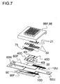
- FIG 7 is an exploded view of the semiconductor module according to the fourth embodiment.
- An IGBT chip 401 and a diode chip 40D are connected with the solder 20 onto an insulation board with fins constituted by brazing the fins 96F, the insulating board 90, the electrodes 60P, 60N, and 60U, and the control wirings 10U and 10D. This allows the chip back sides to be connected to the electrodes.
- the chip top surfaces are connected with the extraction electrodes through the cladding material 30 and connected with the insulation board 98F with fins through the solder 21.
- the double-sided cooling module is configured. It is to be noted that a molding material is not shown in the figure.
- FIG 8 is an illustration of the fifth embodiment of the double-sided cooling module 100.
- This is an example in which the cooling metal plates 96 on which the semiconductor device 40 is brazed are used on both sides so as to cool the semiconductor device from the both sides of the chips and in which two switching circuits are mounted.
- the control terminal 10U of the higher potential side and the output terminal 10D of the lower potential side for switching the higher potential and lower potential sides.
- FIG 9 is an illustration of an implementation example of an inverter (power conversion unit) using the double-sided cooling module 100.
- a plate-like pipe unit 95 with built-in cooling fins is placed on a smoothing capacitor 110 for supplying current when switching.
- the extraction electrodes of the double-sided cooling module 100 are connected and fixed to a connection terminal 112.
- the plate-like pipe unit 95 is fixed with the fixing bracket 97 so as to sandwich the double-sided cooling module 100. At this time, grease with high adhesion and high heat transfer rate may be provided between the pipe unit and the module.
- a control terminal connector 124 connects between a control board 120 and the double-sided cooling module 100.
- a switching control IC122 is mounted on the control board 120 so as to drive a gate of the semiconductor device 40 in the double-sided cooling module.
- the double-sided cooling module 100 includes a circuit in which two switching semiconductor devices are connected in series and has a structure in which voltage is output from a section connected in series so that any one of the both end voltages of the series circuit can be output. For this reason, there is a wiring unit 65 to extract potential from the connected section. This wiring unit 65 is connected to a cable connected to a motor.
- the control board 120 is mounted with a current sensor 126 that monitors current to the motor, and transmits a monitoring result to an external microcomputer board (not shown in the figures) through a connector 128.
- the smoothing capacitor module 110 includes a terminal 114 that connects a cable from a battery, which is a power supply.
- the smoothing capacitor module is provided with a built-in filtering reactor and a built-in discharge resistor in addition to the smoothing capacitor device.
- a conventionally processed semiconductor device semiconductor device having undergone a single-sided plating process
- a power semiconductor module which has a heat dissipation structure to cool the both sides of the semiconductor device and can reduce internal stress.
- This allows a power conversion unit using a small-sized, low-cost semiconductor device to be provided.
- inductance of the power semiconductor module can be reduced, and an increase in volume can be suppressed.
- the power semiconductor module can be improved in reliability.
Landscapes
- Cooling Or The Like Of Semiconductors Or Solid State Devices (AREA)
- Inverter Devices (AREA)
- Lead Frames For Integrated Circuits (AREA)
Abstract
Description
- The disclosure of the following priority application is herein incorporated by reference: Japanese Patent Application No.
2010-086094 filed April 2, 2010 - The present invention relates to a power semiconductor module, in particular a power semiconductor module preferred for a power conversion unit that converts DC power into AC power or AC power into DC power.
- A power conversion unit includes a function to convert DC power supplied from a DC power supply into AC power so as to supply AC power to an AC load such as a rotating electrical machine or a function to convert AC power generated by a rotating electrical machine into DC power so as to supply DC power to a DC power supply.
- To serve such conversion function, the power conversion unit includes an inverter having a semiconductor device with a switching function, and, by repeating conduction and interruption of the semiconductor device, power conversion is performed from DC power to AC power or AC power to DC power.
- The switching semiconductor device generates heat upon switching or upon energization. Due to this, the semiconductor device is mounted on a high thermal conductivity member to form a heat dissipation structure.
- In particular for reducing the power conversion unit in size and cost, it is desirable to adopt a high heat dissipation structure and to reduce the area of the semiconductor device.
- Japanese Laid Open Patent Publication No.
2008-259267 - In addition,
EP 1467607 discloses a structure in which cylindrical metal is soldered on a chip and a metal plate is soldered on a top surface of the metal soldering so that heat is dissipated through both sides of a semiconductor device. - In addition, Japanese Laid Open Patent Publication No.
2000-349207 - However, the stress was not sufficiently reduced inside the power semiconductor module and thus reliability was not sufficiently ensured.
- The present invention is to provide a power semiconductor module with improved reliability.
- A power semiconductor module according to a first aspect of the present invention, wherein: a semiconductor device including electrode surfaces for connection on its front side and back side is connected on its back side to a first extraction electrode through soldering; a metal surface of one side of a laminated conductor having a laminated structure in which at least two types of metals are laminated is directly, intermetallically connected to the front side of the semiconductor device; a second extraction electrode is connected to a metal surface of another side of the laminated conductor through soldering; and the laminated conductor includes a plurality of arch-like protrusions and a straight section connecting the arch-like protrusions, the straight section is connected with the front side of the semiconductor device, and the protrusions are connected with the second extraction electrode.
- According to a second aspect of the present invention, in the power semiconductor module according to the first aspect, the laminated conductor may be a conductor on which copper and aluminium are laminated, an aluminium side of the laminated conductor may be directly metal joined to the front side of the semiconductor device, and a copper side may be joined to the second extraction electrode through soldering.
- According to a third aspect of the present invention, in the power semiconductor module according to the first aspect, it is preferable that the front side of the semiconductor device and the metal surface of the one side of the laminated conductor are ultrasonically connected.
- According to a fourth aspect of the present invention, in the power semiconductor module according to the first aspect, an end of the first extraction electrode may constitute a first terminal for external connection, and an end of the second extraction electrode may constitute a second terminal for external connection.
- According to a fifth aspect of the present invention, in the power semiconductor module according to the first aspect, it is preferable to comprise a first cooling device that cools the power semiconductor module, wherein: the first extraction electrode and the laminated conductor are arranged on a heat receiving surface of the first cooling device through a flat plate-like insulating plate, and the second extraction electrode includes a second cooling device.
- According to a sixth aspect of the present invention, in the power semiconductor module according to the fifth aspect, it is preferable that the first and second cooling devices are metal conductors in which cooling fins are formed.
- In a power semiconductor module according to a seventh aspect, a semiconductor device including electrode surfaces for connection on its front side and back side is connected on its back side to a first extraction electrode through soldering; a metal surface of one side of a laminated conductor having a laminated structure in which at least two types of metals are laminated is directly, intermetallically connected to the front side of the semiconductor device; a second extraction electrode is connected to a metal surface of another side of the laminated conductor through soldering; the laminated conductor includes a plurality of arch-like protrusions and a straight section connecting the arch-like protrusions, the straight section is connected with the front side of the semiconductor device, and the protrusions are connected with the second extraction electrode; the first extraction electrode and the laminated conductor are arranged on a surface of one side of a flat plate-like first cooling device through a flat plate-like insulating plate, and the second extraction electrode is arranged on a surface of one side of a flat plate-like second cooling device; and a capacitor to suppress voltage variations when switching is arranged on a surface of another side of the first cooling device, and a driver board that drives switching of the semiconductor device is arranged on a top surface of the capacitor.
- A power conversion unit according to a eighth aspect of the present invention comprises: a power semiconductor module wherein: a semiconductor device including electrode surfaces for connection on its front side and back side is connected on its back side to a first extraction electrode through soldering; a metal surface of one side of a laminated conductor having a laminated structure in which at least two types of metals are laminated is directly, intermetallically connected to the front side of the semiconductor device; and a second extraction electrode is connected to a metal surface of another side of the laminated conductor through soldering, wherein: the laminated conductor includes a plurality of arch-like protrusions and a straight section connecting the arch-like protrusions, the straight section is connected with the front side of the semiconductor device, and the protrusions are connected with the second extraction electrode; the first extraction electrode and the laminated wiring conductor are arranged on a surface of one side of a flat plate-like first cooling device, inside of which a cooling passage is formed, through a flat plate-like insulating plate, and the second extraction electrode is arranged on a surface of one side of a flat plate-like second cooling device, inside of which a cooling passage is formed; and a capacitor to suppress voltage variations when switching is arranged on a surface of another side of the first cooling device, and a driver board that drives switching of the semiconductor device is arranged on a top surface of the capacitor.
-
-
FIG. 1 is an illustration of a semiconductor module according to an embodiment of the present invention. -
FIG 2 is a connection exploded view of the semiconductor module. -
FIG 3 is an illustration of the first embodiment of a double-sided cooling module. -
FIG 4 is an illustration of the second embodiment of the double-sided cooling module. -
FIG 5 is an illustration of the third embodiment of the double-sided cooling module. -
FIG 6 is an illustration of the fourth embodiment of the double-sided cooling module. -
FIG 7 is an exploded view of the semiconductor module according to the fourth embodiment. -
FIG 8 is an illustration of the fifth embodiment of the double-sided cooling module. -
FIG. 9 is an illustration of an implementation example of an inverter using the double-sided cooling module. - The principle of the present embodiment will now be explained before an embodiment of the present invention is explained.
- In a double-sided cooling structure of a conventional semiconductor device, a high thermal conductivity metal is soldered onto the both sides of the semiconductor device. This causes stress concentration on a soldered section due to a difference in linear expansion coefficient between the semiconductor device and the soldered high thermal conductivity metal with increasing temperature in the semiconductor device, thereby causing a crack or the like to occur with long-term use. Because of this, the periphery of the metal is bonded with a resin so as to prevent the metal section from expanding, and the metal is brazed with ceramic to reduce an apparent coefficient of thermal expansion so as to reduce stress to the solder, thereby preventing life degradation.
- However, since the double-sided cooling structure is a structure in which the semiconductor device is sandwiched by metal from the both sides, stress is directly applied to the semiconductor device and the solder when assembling or implementing an inverter, and those may be cracked.
- In addition, production of the semiconductor device requires plating to solder the both sides, thereby making the processing more complicated than a conventional single-sided process.
- On the surface of the semiconductor device, there are regions of an electrode pad for switching control, an electrode pad for a current sensor or a temperature sensor, and the like. In addition to those regions, on the outer circumference of the semiconductor device, there is a region in which device voltage-resistance is ensured, and it is necessary to prevent those regions from shorting out or being contaminated. As a result, plating for soldering both sides not only increases plating cost but also reduces reliability and yield, thereby increasing cost. In addition, it has a heavy environmental load such as plating rinse water treatment.
- In view of those problems, the present invention is to provide a power semiconductor module having a heat dissipation structure in which the both sides of the semiconductor device are cooled by using a semiconductor device having undergone a single-sided plating process and reducing internal stress.
- Since the present embodiment includes the following structure, a heat dissipation structure can be achieved in which the semiconductor device constituting a power semiconductor module can be cooled on the both sides and internal stress can be reduced, using a semiconductor device having undergone a single-sided plating process.
- The embodiment will now be explained with reference to the attached drawings.
-
FIG 1 is an illustration of a semiconductor module according to the present embodiment. In addition,FIG 2 is a connection exploded view of the semiconductor module. - A
semiconductor device 40 is connected to anexternal extraction electrode 60 through asolder 20 on its bottom electrode, and the top control electrode of thesemiconductor device 40 is connected to an external extraction electrode (control terminal) 70 through acontrol wire 75. - A
cladding material 30 including two types of metal layers is ultrasonically connected to the top electrode of the semiconductor device. The top electrode of the high-current semiconductor device 40 is made of aluminium. Thecladding material 30 is constituted with the two layers of analuminium 33 and acopper 32, thealuminium 33 side of which faces the top surface of the semiconductor device so as to enable ultrasonic welding. After this ultrasonic welding, anexternal extraction electrode 10 and thecopper 32 side of thecladding material 30 are joined with asolder 21. In addition, their exterior is solidified with amold resin 80. Thus, a double-sidedcooling module 100 is configured in which thesemiconductor device 40 can be cooled on the top side and the bottom side. Thecladding material 30 is a thin flat plate whose thickness is configured to be equal to or less than 0.2 mm so as to facilitate transmission of a ultrasonic frequency to a joint interface, as in a conventional ultrasonic connection, thereby ensuring connection with the top surface of thesemiconductor device 40. - Here, the
cladding material 30 is constituted with anarch section 35 and astraight section 36 so that the upper side of thesemiconductor device 40 can be divided into thestraight section 36 to be ultrasonically connected and thearch section 35 to be connected with thesolder 21. Thisarch section 35 can relieve stress applied from the upper side of thesemiconductor device 40. - A section of the
cladding material 30 to be connected to theexternal extraction electrode 10 is arched so that even if, when connecting with theelectrode 10, a variation in thickness of thesolder 20 causes thesemiconductor device 40 to lean and thus causes a variation in height, thearch section 35 is deformed so as to accommodate the variations. This can provide a secure soldering connection between thecladding material 30 and theelectrode 10. - Thus, the surface of the
semiconductor device 40 and thestraight section 36 of thecladding material 30 are once ultrasonically connected so as to provide a connection to reliably cool the both sides of thesemiconductor device 40 compared to a conventional double-sided cooling structure, in which a surface of a semiconductor device is directly soldered. In addition, thesemiconductor device 40 may undergo a conventional process. More specifically, the surface may not be provided with plating for soldering, thereby preventing an increase in cost and reduction in yield. - The
control terminal 70 is a terminal at which voltage for switching on or off thesemiconductor device 40 is applied from the outside, and is connected with thesemiconductor device 40 through thecontrol terminal wire 75 such as an aluminium wire. While in this figure theterminal 70 is illustrated between theextraction electrodes terminal 70 is provided on the same plane as theelectrode 60 and the wiring is provided when the top surface of thesemiconductor device 40 is seen, i.e., before theelectrode 10 is connected with thesolder 21, as shown inFIG 2 . -
FIG 3 is an illustration of the first embodiment of the double-sided cooling module 100. The top and bottom surfaces of the double-sided cooling module 100 are sandwiched by coolingfins 95 through insulatingplates 90 and fixed with a fixingbracket 97. Here, a plurality of the fixingbrackets 97 are disposed so as to uniformly pressurize the double-sided cooling module 100. - The insulating
plates 90 are made of ceramic such as aluminium nitride, silicon nitride, and alumina or high thermal conductivity resin. When made of ceramic, the insulatingplates 90 may be brazed to the coolingfins 95. The insulatingplates 90 brazed to both the coolingfins 95 and the external extraction electrode may be used. When made of resin, the insulatingplates 90 adhered to the coolingfins 95 in advance may be used. -
FIG 4 is an illustration of the second embodiment of the double-sided cooling module 100. As shown in the figure, thesemiconductor device 40 is connected through thesolder 20 to the top surface of aninsulation metal board 98 in which theextraction electrodes plate 90 and a coolingmetal plate 96 is brazed onto the bottom surface of the insulatingplate 90. Thealuminium 33 side of thecladding material 30 is ultrasonically connected to theelectrode 10 of thesemiconductor device 40. In addition, a coolingmetal plate 15 is connected through thesolder 21 to thecopper 32 side of thecladding material 30. This allows a current path and a cooling path of the top surface of the semiconductor device to be separated. This allows heat generation due to current flowing through the cooling path itself of the top surface of thesemiconductor device 40 to be reduced. In addition, the top surface cooling structure can be achieved in a structure similar to a conventional semiconductor module. It is to be noted that thecontrol terminal 70 is curtailed in this figure. In addition, the coolingmetal plate 15 of the top surface can be replaced with aninsulation metal board 98. -
FIG. 5 is an illustration of the third embodiment of the double-sided cooling module 100. Aninsulation board 98F with fins is utilized, which is configured by brazing theelectrodes board 90 and brazing a coolingmetal plate 96F with fins onto the bottom surface of the insulatingboard 90, and thesemiconductor device 40 is connected through thesolder 20 to an electrode 2. Thealuminium 33 side of thecladding material 30 is ultrasonically connected to thesemiconductor device 40 and theelectrode 10. In addition, the coolingmetal plate 15 is connected through thesolder 21 to thecopper 32 side of thecladding material 30. It is to be noted that the coolingmetal plate 15 of the top surface can be replaced with aninsulation metal board 98F with fins. -
FIG. 6 is an illustration of the fourth embodiment of the double-sided cooling module 100. This is an example in which theinsulation board 98F with fins are used on both sides and two switching circuits are mounted. There are external terminals of a terminal 60P connected to a higher potential side, a terminal 60N connected to a lower potential side, and a terminal 60U that outputs higher potential or lower potential depending upon switching. In addition, acontrol terminal 10U of the higher potential side and anoutput terminal 10D of the lower potential side are provided to drive switching circuits of the higher potential side and the lower potential side. -
FIG 7 is an exploded view of the semiconductor module according to the fourth embodiment. AnIGBT chip 401 and adiode chip 40D are connected with thesolder 20 onto an insulation board with fins constituted by brazing thefins 96F, the insulatingboard 90, theelectrodes control wirings cladding material 30 and connected with theinsulation board 98F with fins through thesolder 21. Thus the double-sided cooling module is configured. It is to be noted that a molding material is not shown in the figure. -
FIG 8 is an illustration of the fifth embodiment of the double-sided cooling module 100. This is an example in which the coolingmetal plates 96 on which thesemiconductor device 40 is brazed are used on both sides so as to cool the semiconductor device from the both sides of the chips and in which two switching circuits are mounted. There are external terminals of the terminal 60P connected to the higher potential side, the terminal 60N connected to the lower potential side, and the terminal 60U that outputs higher potential or lower potential depending upon switching. In addition, there are thecontrol terminal 10U of the higher potential side and theoutput terminal 10D of the lower potential side for switching the higher potential and lower potential sides. -
FIG 9 is an illustration of an implementation example of an inverter (power conversion unit) using the double-sided cooling module 100. A plate-like pipe unit 95 with built-in cooling fins is placed on a smoothingcapacitor 110 for supplying current when switching. The extraction electrodes of the double-sided cooling module 100 are connected and fixed to aconnection terminal 112. - The plate-
like pipe unit 95 is fixed with the fixingbracket 97 so as to sandwich the double-sided cooling module 100. At this time, grease with high adhesion and high heat transfer rate may be provided between the pipe unit and the module. In addition, acontrol terminal connector 124 connects between acontrol board 120 and the double-sided cooling module 100. A switching control IC122 is mounted on thecontrol board 120 so as to drive a gate of thesemiconductor device 40 in the double-sided cooling module. - The double-
sided cooling module 100 includes a circuit in which two switching semiconductor devices are connected in series and has a structure in which voltage is output from a section connected in series so that any one of the both end voltages of the series circuit can be output. For this reason, there is awiring unit 65 to extract potential from the connected section. Thiswiring unit 65 is connected to a cable connected to a motor. Thecontrol board 120 is mounted with acurrent sensor 126 that monitors current to the motor, and transmits a monitoring result to an external microcomputer board (not shown in the figures) through aconnector 128. - The smoothing
capacitor module 110 includes a terminal 114 that connects a cable from a battery, which is a power supply. The smoothing capacitor module is provided with a built-in filtering reactor and a built-in discharge resistor in addition to the smoothing capacitor device. - As explained above, according to the semiconductor module of the present embodiments, a conventionally processed semiconductor device (semiconductor device having undergone a single-sided plating process) is used to provide a power semiconductor module which has a heat dissipation structure to cool the both sides of the semiconductor device and can reduce internal stress. This allows a power conversion unit using a small-sized, low-cost semiconductor device to be provided. In addition, inductance of the power semiconductor module can be reduced, and an increase in volume can be suppressed.
- According to the above embodiments, the power semiconductor module can be improved in reliability.
- The above described embodiments are examples, and various modifications can be made without departing from the scope of the invention.
Claims (8)
- A power semiconductor module, wherein:a semiconductor device including electrode surfaces for connection on its front side and back side is connected on its back side to a first extraction electrode through soldering;a metal surface of one side of a laminated conductor having a laminated structure in which at least two types of metals are laminated is directly, intermetallically connected to the front side of the semiconductor device;a second extraction electrode is connected to a metal surface of another side of the laminated conductor through soldering; andthe laminated conductor includes a plurality of arch-like protrusions and a straight section connecting the arch-like protrusions, the straight section is connected with the front side of the semiconductor device, and the protrusions are connected with the second extraction electrode.
- A power semiconductor module according to claim 1, wherein:the laminated conductor is a conductor on which copper and aluminium are laminated, an aluminium side of the laminated conductor is directly metal joined to the front side of the semiconductor device, and a copper side is joined to the second extraction electrode through soldering.
- A power semiconductor module according to claim 1, wherein:the front side of the semiconductor device and the metal surface of the one side of the laminated conductor are ultrasonically connected.
- A power semiconductor module according to claim 1, wherein:an end of the first extraction electrode constitutes a first terminal for external connection, and an end of the second extraction electrode constitutes a second terminal for external connection.
- A power semiconductor module according to claim 1, comprising:a first cooling device that cools the power semiconductor module, wherein:the first extraction electrode and the laminated conductor are arranged on a heat receiving surface of the first cooling device through a flat plate-like insulating plate, and the second extraction electrode includes a second cooling device.
- A power semiconductor module according to claim 5, wherein:the first and second cooling devices are metal conductors in which cooling fins are formed.
- A power semiconductor module, wherein:a semiconductor device including electrode surfaces for connection on its front side and back side is connected on its back side to a first extraction electrode through soldering;a metal surface of one side of a laminated conductor having a laminated structure in which at least two types of metals are laminated is directly, intermetallically connected to the front side of the semiconductor device;a second extraction electrode is connected to a metal surface of another side of the laminated conductor through soldering;the laminated conductor includes a plurality of arch-like protrusions and a straight section connecting the arch-like protrusions, the straight section is connected with the front side of the semiconductor device, and the protrusions are connected with the second extraction electrode;the first extraction electrode and the laminated conductor are arranged on a surface of one side of a flat plate-like first cooling device through a flat plate-like insulating plate, and the second extraction electrode is arranged on a surface of one side of a flat plate-like second cooling device; anda capacitor to suppress voltage variations when switching is arranged on a surface of another side of the first cooling device, and a driver board that drives switching of the semiconductor device is arranged on a top surface of the capacitor.
- A power conversion unit, comprising:a power semiconductor module wherein:a semiconductor device including electrode surfaces for connection on its front side and back side is connected on its back side to a first extraction electrode through soldering;a metal surface of one side of a laminated conductor having a laminated structure in which at least two types of metals are laminated is directly, intermetallically connected to the front side of the semiconductor device; anda second extraction electrode is connected to a metal surface of another side of the laminated conductor through soldering, wherein:the laminated conductor includes a plurality of arch-like protrusions and a straight section connecting the arch-like protrusions, the straight section is connected with the front side of the semiconductor device, and the protrusions are connected with the second extraction electrode;the first extraction electrode and the laminated wiring conductor are arranged on a surface of one side of a flat plate-like first cooling device, inside of which a cooling passage is formed, through a flat plate-like insulating plate, and the second extraction electrode is arranged on a surface of one side of a flat plate-like second cooling device, inside of which a cooling passage is formed; anda capacitor to suppress voltage variations when switching is arranged on a surface of another side of the first cooling device, and a driver board that drives switching of the semiconductor device is arranged on a top surface of the capacitor.
Applications Claiming Priority (1)
| Application Number | Priority Date | Filing Date | Title |
|---|---|---|---|
| JP2010086094A JP5473733B2 (en) | 2010-04-02 | 2010-04-02 | Power semiconductor module |
Publications (2)
| Publication Number | Publication Date |
|---|---|
| EP2372763A2 true EP2372763A2 (en) | 2011-10-05 |
| EP2372763A3 EP2372763A3 (en) | 2016-07-27 |
Family
ID=44202901
Family Applications (1)
| Application Number | Title | Priority Date | Filing Date |
|---|---|---|---|
| EP11160367.6A Withdrawn EP2372763A3 (en) | 2010-04-02 | 2011-03-30 | Power semiconductor module |
Country Status (3)
| Country | Link |
|---|---|
| US (1) | US8294258B2 (en) |
| EP (1) | EP2372763A3 (en) |
| JP (1) | JP5473733B2 (en) |
Cited By (6)
| Publication number | Priority date | Publication date | Assignee | Title |
|---|---|---|---|---|
| NL2025200A (en) * | 2019-04-10 | 2020-10-15 | Shindengen Electric Mfg | Semiconductor device |
| WO2020225097A1 (en) * | 2019-05-08 | 2020-11-12 | Danfoss Silicon Power Gmbh | Semiconductor module comprising a semiconductor body electrically contected to a shaped metal body, as well as the method of obtaining the same |
| EP3732719A4 (en) * | 2017-12-29 | 2021-11-17 | Intel Corporation | MICROELECTRONIC ASSEMBLIES |
| IT202100008036A1 (en) * | 2021-03-31 | 2022-10-01 | St Microelectronics Srl | CONNECTOR STRIP FOR DISCRETE AND/OR POWER ELECTRONIC DEVICES AND THE DISCRETE AND/OR POWER ELECTRONIC DEVICE CONNECTED THROUGH SUCH CONNECTOR STRIP |
| DE102022205701A1 (en) | 2022-06-03 | 2023-12-14 | Zf Friedrichshafen Ag | POWER ELEMENT INTEGRATION MODULE |
| US12125817B2 (en) | 2019-05-08 | 2024-10-22 | Danfoss Silicon Power Gmbh | Semiconductor module with a first substrate, a second substrate and a spacer separating the substrates from each other |
Families Citing this family (29)
| Publication number | Priority date | Publication date | Assignee | Title |
|---|---|---|---|---|
| JP5120284B2 (en) * | 2009-02-04 | 2013-01-16 | 株式会社豊田自動織機 | Semiconductor device |
| JP5489911B2 (en) * | 2010-08-18 | 2014-05-14 | 三菱電機株式会社 | Semiconductor power module |
| KR101278393B1 (en) * | 2010-11-01 | 2013-06-24 | 삼성전기주식회사 | Power package module and a fabricating mothod the same |
| US8804340B2 (en) * | 2011-06-08 | 2014-08-12 | International Rectifier Corporation | Power semiconductor package with double-sided cooling |
| JP5370448B2 (en) * | 2011-09-19 | 2013-12-18 | 株式会社デンソー | Power converter |
| DE112012005472T5 (en) * | 2011-12-26 | 2014-09-11 | Mitsubishi Electric Corporation | Electric power semiconductor device and method of manufacturing the same |
| US8786111B2 (en) | 2012-05-14 | 2014-07-22 | Infineon Technologies Ag | Semiconductor packages and methods of formation thereof |
| DE102012211446B4 (en) * | 2012-07-02 | 2016-05-12 | Infineon Technologies Ag | EXPLOSION-PROTECTED SEMICONDUCTOR MODULE |
| CN104604115B (en) * | 2013-05-21 | 2019-05-03 | 日立汽车系统株式会社 | power conversion device |
| US9899345B2 (en) | 2014-01-27 | 2018-02-20 | Mitsubishi Electric Cooperation | Electrode terminal, semiconductor device for electrical power, and method for manufacturing semiconductor device for electrical power |
| WO2016067377A1 (en) * | 2014-10-29 | 2016-05-06 | 新電元工業株式会社 | Heat-dissipating structure |
| CN105244331A (en) * | 2015-10-10 | 2016-01-13 | 杰群电子科技(东莞)有限公司 | Chip package structure |
| DE102015122259B4 (en) | 2015-12-18 | 2020-12-24 | Infineon Technologies Austria Ag | Semiconductor devices having a porous insulating layer |
| JP6685143B2 (en) * | 2016-02-03 | 2020-04-22 | 三菱電機株式会社 | Electrode terminal, semiconductor device and power converter |
| JP6689708B2 (en) | 2016-08-10 | 2020-04-28 | ルネサスエレクトロニクス株式会社 | Electronic device |
| JP6860334B2 (en) * | 2016-12-06 | 2021-04-14 | 株式会社東芝 | Semiconductor device |
| WO2018146816A1 (en) * | 2017-02-13 | 2018-08-16 | 新電元工業株式会社 | Electronic device |
| JP7159620B2 (en) * | 2018-05-30 | 2022-10-25 | 富士電機株式会社 | Semiconductor devices, cooling modules, power converters and electric vehicles |
| EP3859775A1 (en) * | 2020-02-03 | 2021-08-04 | Infineon Technologies AG | Semiconductor arrangement and method for producing the same |
| DE112021000342T5 (en) * | 2020-02-27 | 2022-09-22 | Panasonic Intellectual Property Management Co., Ltd. | SEMICONDUCTOR LASER DEVICE |
| CN112289763A (en) * | 2020-06-12 | 2021-01-29 | 无锡利普思半导体有限公司 | Power semiconductor module |
| CN112038245B (en) * | 2020-07-22 | 2022-11-18 | 无锡利普思半导体有限公司 | Connection process of internal binding line of power module |
| JP7615592B2 (en) * | 2020-09-30 | 2025-01-17 | ニデック株式会社 | Power Module |
| JP7624913B2 (en) * | 2021-11-25 | 2025-01-31 | 三菱電機株式会社 | Semiconductor Device |
| GB2613794B (en) | 2021-12-14 | 2026-03-25 | Zhuzhou Crrc Times Electric Co Ltd | Power semiconductor module |
| EP4213203B1 (en) * | 2022-01-12 | 2026-03-04 | Nexperia B.V. | Semiconductor device package and method for manufacturing the same |
| JP2024046339A (en) * | 2022-09-22 | 2024-04-03 | 株式会社東芝 | Semiconductor Device |
| JP2024094121A (en) * | 2022-12-27 | 2024-07-09 | 日立Astemo株式会社 | Electrical circuit and power conversion device |
| DE102023123825A1 (en) | 2023-09-05 | 2025-03-06 | Infineon Technologies Ag | Package with transistor chip between carrier and conductive structure and with thermally conductive electrically insulating layer |
Citations (4)
| Publication number | Priority date | Publication date | Assignee | Title |
|---|---|---|---|---|
| JP2000349207A (en) | 1999-06-02 | 2000-12-15 | Denso Corp | Semiconductor device mounting structure and mounting method |
| EP1467607A1 (en) | 2003-04-09 | 2004-10-13 | Alstom | Power switch module and inverter with such a module |
| JP2008259267A (en) | 2007-04-02 | 2008-10-23 | Hitachi Ltd | Semiconductor module for inverter circuit |
| JP2010086094A (en) | 2008-09-30 | 2010-04-15 | Kenwood Corp | Content processing device, content display method, and program |
Family Cites Families (19)
| Publication number | Priority date | Publication date | Assignee | Title |
|---|---|---|---|---|
| US6040626A (en) * | 1998-09-25 | 2000-03-21 | International Rectifier Corp. | Semiconductor package |
| JP4112816B2 (en) * | 2001-04-18 | 2008-07-02 | 株式会社東芝 | Semiconductor device and manufacturing method of semiconductor device |
| US6747342B1 (en) * | 2002-08-09 | 2004-06-08 | Lovoltech, Inc. | Flip-chip packaging |
| US20040217488A1 (en) * | 2003-05-02 | 2004-11-04 | Luechinger Christoph B. | Ribbon bonding |
| EP2216891B1 (en) * | 2003-08-21 | 2012-01-04 | Denso Corporation | Mounting structure ofa semiconductor device |
| JP2006190972A (en) * | 2004-12-08 | 2006-07-20 | Mitsubishi Electric Corp | Power semiconductor device |
| JP4645276B2 (en) * | 2005-04-12 | 2011-03-09 | 富士電機システムズ株式会社 | Semiconductor device |
| US7683464B2 (en) * | 2005-09-13 | 2010-03-23 | Alpha And Omega Semiconductor Incorporated | Semiconductor package having dimpled plate interconnections |
| DE102005049687B4 (en) * | 2005-10-14 | 2008-09-25 | Infineon Technologies Ag | Power semiconductor component in flat conductor technology with vertical current path and method for the production |
| US7285849B2 (en) * | 2005-11-18 | 2007-10-23 | Fairchild Semiconductor Corporation | Semiconductor die package using leadframe and clip and method of manufacturing |
| FR2896914B1 (en) * | 2006-01-30 | 2008-07-04 | Valeo Electronique Sys Liaison | ELECTRONIC MODULE AND METHOD FOR ASSEMBLING SUCH A MODULE |
| DE102006015447B4 (en) * | 2006-03-31 | 2012-08-16 | Infineon Technologies Ag | Power semiconductor component with a power semiconductor chip and method for producing the same |
| WO2007125939A1 (en) * | 2006-04-27 | 2007-11-08 | Neomax Materials Co., Ltd. | Clad material for wiring connection and wiring connection member processed from the clad material |
| US8552543B2 (en) * | 2006-11-13 | 2013-10-08 | International Rectifier Corporation | Semiconductor package |
| DE102006060484B4 (en) * | 2006-12-19 | 2012-03-08 | Infineon Technologies Ag | Semiconductor device with a semiconductor chip and method for producing the same |
| TWI456707B (en) * | 2008-01-28 | 2014-10-11 | 瑞薩電子股份有限公司 | Semiconductor device and method of manufacturing same |
| JP4748173B2 (en) * | 2008-03-04 | 2011-08-17 | 株式会社デンソー | Semiconductor module and manufacturing method thereof |
| US8450845B2 (en) * | 2008-04-09 | 2013-05-28 | Fuji Electric Co., Ltd. | Semiconductor device |
| US8049312B2 (en) * | 2009-01-12 | 2011-11-01 | Texas Instruments Incorporated | Semiconductor device package and method of assembly thereof |
-
2010
- 2010-04-02 JP JP2010086094A patent/JP5473733B2/en not_active Expired - Fee Related
-
2011
- 2011-03-30 EP EP11160367.6A patent/EP2372763A3/en not_active Withdrawn
- 2011-04-01 US US13/078,135 patent/US8294258B2/en not_active Expired - Fee Related
Patent Citations (4)
| Publication number | Priority date | Publication date | Assignee | Title |
|---|---|---|---|---|
| JP2000349207A (en) | 1999-06-02 | 2000-12-15 | Denso Corp | Semiconductor device mounting structure and mounting method |
| EP1467607A1 (en) | 2003-04-09 | 2004-10-13 | Alstom | Power switch module and inverter with such a module |
| JP2008259267A (en) | 2007-04-02 | 2008-10-23 | Hitachi Ltd | Semiconductor module for inverter circuit |
| JP2010086094A (en) | 2008-09-30 | 2010-04-15 | Kenwood Corp | Content processing device, content display method, and program |
Cited By (11)
| Publication number | Priority date | Publication date | Assignee | Title |
|---|---|---|---|---|
| EP3732719A4 (en) * | 2017-12-29 | 2021-11-17 | Intel Corporation | MICROELECTRONIC ASSEMBLIES |
| NL2025200A (en) * | 2019-04-10 | 2020-10-15 | Shindengen Electric Mfg | Semiconductor device |
| WO2020225097A1 (en) * | 2019-05-08 | 2020-11-12 | Danfoss Silicon Power Gmbh | Semiconductor module comprising a semiconductor body electrically contected to a shaped metal body, as well as the method of obtaining the same |
| US12125817B2 (en) | 2019-05-08 | 2024-10-22 | Danfoss Silicon Power Gmbh | Semiconductor module with a first substrate, a second substrate and a spacer separating the substrates from each other |
| US12581983B2 (en) | 2019-05-08 | 2026-03-17 | Danfoss Silicon Power Gmbh | Semiconductor module comprising a semiconductor and comprising a shaped metal body that is electrically contacted by the semiconductor |
| IT202100008036A1 (en) * | 2021-03-31 | 2022-10-01 | St Microelectronics Srl | CONNECTOR STRIP FOR DISCRETE AND/OR POWER ELECTRONIC DEVICES AND THE DISCRETE AND/OR POWER ELECTRONIC DEVICE CONNECTED THROUGH SUCH CONNECTOR STRIP |
| EP4068351A2 (en) | 2021-03-31 | 2022-10-05 | STMicroelectronics S.r.l. | Connecting strip for discrete or power electronic devices and a connection method using the same |
| US20220320032A1 (en) * | 2021-03-31 | 2022-10-06 | Stmicroelectronics S.R.L. | Connecting strip for discrete and power electronic devices |
| EP4068351A3 (en) * | 2021-03-31 | 2023-06-07 | STMicroelectronics S.r.l. | Connecting strip for discrete or power electronic devices and a connection method using the same |
| US12374648B2 (en) * | 2021-03-31 | 2025-07-29 | Stmicroelectronics S.R.L. | Connecting strip for discrete and power electronic devices |
| DE102022205701A1 (en) | 2022-06-03 | 2023-12-14 | Zf Friedrichshafen Ag | POWER ELEMENT INTEGRATION MODULE |
Also Published As
| Publication number | Publication date |
|---|---|
| JP5473733B2 (en) | 2014-04-16 |
| EP2372763A3 (en) | 2016-07-27 |
| JP2011216822A (en) | 2011-10-27 |
| US20110241198A1 (en) | 2011-10-06 |
| US8294258B2 (en) | 2012-10-23 |
Similar Documents
| Publication | Publication Date | Title |
|---|---|---|
| US8294258B2 (en) | Power semiconductor module | |
| JP7204770B2 (en) | Double-sided cooling power module and manufacturing method thereof | |
| CN100394602C (en) | Electronic circuit device and manufacturing method thereof | |
| US10128167B2 (en) | Semiconductor module and manufacturing method of semiconductor module | |
| US8659147B2 (en) | Power semiconductor circuit device and method for manufacturing the same | |
| US7151661B2 (en) | Capacitor module and semiconductor device using the same | |
| EP1843392A1 (en) | Electronics assembly having heat sink substrate disposed in cooling vessel | |
| JP6881238B2 (en) | Semiconductor module, its manufacturing method and power converter | |
| CN110364497B (en) | Electronic device module for power control and method of manufacturing the same | |
| TWI295368B (en) | ||
| JP5217884B2 (en) | Semiconductor device | |
| JP3646665B2 (en) | Inverter device | |
| JP5895220B2 (en) | Manufacturing method of semiconductor device | |
| JP7196047B2 (en) | ELECTRICAL CIRCUIT, POWER CONVERTER, AND METHOD OF MANUFACTURING ELECTRICAL CIRCUIT | |
| US6906935B2 (en) | Inverter apparatus and method of manufacturing the same | |
| WO2015141284A1 (en) | Semiconductor module unit and semiconductor module | |
| JPH1189248A (en) | Power control device | |
| WO2022123870A1 (en) | Electrical circuit body, power conversion device, and electrical circuit body manufacturing method | |
| WO2019216161A1 (en) | Power semiconductor module, method for producing same and electric power converter | |
| CN1961474B (en) | Converter device | |
| JP2008042074A (en) | Semiconductor device and power conversion device | |
| US20100102431A1 (en) | Power module and inverter for vehicles | |
| CN114586151A (en) | Semiconductor device, power conversion device, and method for manufacturing semiconductor device | |
| CN114730748A (en) | Power module with encapsulated power semiconductor for the controlled supply of electrical power to consumers and method for producing the same | |
| CN108496247A (en) | Semiconductor device |
Legal Events
| Date | Code | Title | Description |
|---|---|---|---|
| PUAI | Public reference made under article 153(3) epc to a published international application that has entered the european phase |
Free format text: ORIGINAL CODE: 0009012 |
|
| 17P | Request for examination filed |
Effective date: 20110801 |
|
| AK | Designated contracting states |
Kind code of ref document: A2 Designated state(s): AL AT BE BG CH CY CZ DE DK EE ES FI FR GB GR HR HU IE IS IT LI LT LU LV MC MK MT NL NO PL PT RO RS SE SI SK SM TR |
|
| AX | Request for extension of the european patent |
Extension state: BA ME |
|
| PUAL | Search report despatched |
Free format text: ORIGINAL CODE: 0009013 |
|
| AK | Designated contracting states |
Kind code of ref document: A3 Designated state(s): AL AT BE BG CH CY CZ DE DK EE ES FI FR GB GR HR HU IE IS IT LI LT LU LV MC MK MT NL NO PL PT RO RS SE SI SK SM TR |
|
| AX | Request for extension of the european patent |
Extension state: BA ME |
|
| RIC1 | Information provided on ipc code assigned before grant |
Ipc: H01L 23/473 20060101ALI20160622BHEP Ipc: H01L 23/367 20060101ALI20160622BHEP Ipc: H01L 23/31 20060101ALI20160622BHEP Ipc: H01L 23/00 20060101ALI20160622BHEP Ipc: H01L 23/433 20060101ALI20160622BHEP Ipc: H01L 25/11 20060101ALI20160622BHEP Ipc: H01L 25/07 20060101AFI20160622BHEP Ipc: H01L 23/495 20060101ALI20160622BHEP Ipc: H01L 23/051 20060101ALI20160622BHEP |
|
| STAA | Information on the status of an ep patent application or granted ep patent |
Free format text: STATUS: THE APPLICATION HAS BEEN WITHDRAWN |
|
| 18W | Application withdrawn |
Effective date: 20170512 |