EP2369725B1 - Dispositif de court-circuit - Google Patents
Dispositif de court-circuit Download PDFInfo
- Publication number
- EP2369725B1 EP2369725B1 EP10157722A EP10157722A EP2369725B1 EP 2369725 B1 EP2369725 B1 EP 2369725B1 EP 10157722 A EP10157722 A EP 10157722A EP 10157722 A EP10157722 A EP 10157722A EP 2369725 B1 EP2369725 B1 EP 2369725B1
- Authority
- EP
- European Patent Office
- Prior art keywords
- power
- converter
- designed
- electronic switch
- drive
- Prior art date
- Legal status (The legal status is an assumption and is not a legal conclusion. Google has not performed a legal analysis and makes no representation as to the accuracy of the status listed.)
- Active
Links
- 238000001514 detection method Methods 0.000 claims description 5
- 238000012544 monitoring process Methods 0.000 claims description 4
- 239000004065 semiconductor Substances 0.000 claims description 4
- 238000006243 chemical reaction Methods 0.000 claims description 3
- 239000003990 capacitor Substances 0.000 description 20
- 238000004146 energy storage Methods 0.000 description 8
- 238000000034 method Methods 0.000 description 4
- 238000010586 diagram Methods 0.000 description 3
- 238000005259 measurement Methods 0.000 description 2
- 230000001681 protective effect Effects 0.000 description 2
- 240000001439 Opuntia Species 0.000 description 1
- 235000004727 Opuntia ficus indica Nutrition 0.000 description 1
- 101100509645 Ustilago maydis (strain 521 / FGSC 9021) PKAR gene Proteins 0.000 description 1
- 101100497638 Ustilago maydis (strain 521 / FGSC 9021) UAC1 gene Proteins 0.000 description 1
- 230000004913 activation Effects 0.000 description 1
- 238000005275 alloying Methods 0.000 description 1
- 230000005540 biological transmission Effects 0.000 description 1
- 241001233037 catfish Species 0.000 description 1
- 230000007423 decrease Effects 0.000 description 1
- 230000002950 deficient Effects 0.000 description 1
- 230000001419 dependent effect Effects 0.000 description 1
- 238000003745 diagnosis Methods 0.000 description 1
- 238000005516 engineering process Methods 0.000 description 1
- 238000010304 firing Methods 0.000 description 1
- 238000010348 incorporation Methods 0.000 description 1
- 238000002955 isolation Methods 0.000 description 1
- 230000007257 malfunction Effects 0.000 description 1
- 230000007246 mechanism Effects 0.000 description 1
- 230000008569 process Effects 0.000 description 1
- 238000012545 processing Methods 0.000 description 1
- 230000009467 reduction Effects 0.000 description 1
- 230000004044 response Effects 0.000 description 1
Images

Classifications
-
- H—ELECTRICITY
- H02—GENERATION; CONVERSION OR DISTRIBUTION OF ELECTRIC POWER
- H02M—APPARATUS FOR CONVERSION BETWEEN AC AND AC, BETWEEN AC AND DC, OR BETWEEN DC AND DC, AND FOR USE WITH MAINS OR SIMILAR POWER SUPPLY SYSTEMS; CONVERSION OF DC OR AC INPUT POWER INTO SURGE OUTPUT POWER; CONTROL OR REGULATION THEREOF
- H02M1/00—Details of apparatus for conversion
- H02M1/32—Means for protecting converters other than automatic disconnection
-
- H—ELECTRICITY
- H02—GENERATION; CONVERSION OR DISTRIBUTION OF ELECTRIC POWER
- H02M—APPARATUS FOR CONVERSION BETWEEN AC AND AC, BETWEEN AC AND DC, OR BETWEEN DC AND DC, AND FOR USE WITH MAINS OR SIMILAR POWER SUPPLY SYSTEMS; CONVERSION OF DC OR AC INPUT POWER INTO SURGE OUTPUT POWER; CONTROL OR REGULATION THEREOF
- H02M5/00—Conversion of ac power input into ac power output, e.g. for change of voltage, for change of frequency, for change of number of phases
- H02M5/40—Conversion of ac power input into ac power output, e.g. for change of voltage, for change of frequency, for change of number of phases with intermediate conversion into dc
- H02M5/42—Conversion of ac power input into ac power output, e.g. for change of voltage, for change of frequency, for change of number of phases with intermediate conversion into dc by static converters
- H02M5/44—Conversion of ac power input into ac power output, e.g. for change of voltage, for change of frequency, for change of number of phases with intermediate conversion into dc by static converters using discharge tubes or semiconductor devices to convert the intermediate dc into ac
- H02M5/453—Conversion of ac power input into ac power output, e.g. for change of voltage, for change of frequency, for change of number of phases with intermediate conversion into dc by static converters using discharge tubes or semiconductor devices to convert the intermediate dc into ac using devices of a triode or transistor type requiring continuous application of a control signal
- H02M5/458—Conversion of ac power input into ac power output, e.g. for change of voltage, for change of frequency, for change of number of phases with intermediate conversion into dc by static converters using discharge tubes or semiconductor devices to convert the intermediate dc into ac using devices of a triode or transistor type requiring continuous application of a control signal using semiconductor devices only
-
- H—ELECTRICITY
- H02—GENERATION; CONVERSION OR DISTRIBUTION OF ELECTRIC POWER
- H02M—APPARATUS FOR CONVERSION BETWEEN AC AND AC, BETWEEN AC AND DC, OR BETWEEN DC AND DC, AND FOR USE WITH MAINS OR SIMILAR POWER SUPPLY SYSTEMS; CONVERSION OF DC OR AC INPUT POWER INTO SURGE OUTPUT POWER; CONTROL OR REGULATION THEREOF
- H02M7/00—Conversion of ac power input into dc power output; Conversion of dc power input into ac power output
- H02M7/42—Conversion of dc power input into ac power output without possibility of reversal
- H02M7/44—Conversion of dc power input into ac power output without possibility of reversal by static converters
- H02M7/48—Conversion of dc power input into ac power output without possibility of reversal by static converters using discharge tubes with control electrode or semiconductor devices with control electrode
- H02M7/483—Converters with outputs that each can have more than two voltages levels
- H02M7/4835—Converters with outputs that each can have more than two voltages levels comprising two or more cells, each including a switchable capacitor, the capacitors having a nominal charge voltage which corresponds to a given fraction of the input voltage, and the capacitors being selectively connected in series to determine the instantaneous output voltage
-
- H—ELECTRICITY
- H02—GENERATION; CONVERSION OR DISTRIBUTION OF ELECTRIC POWER
- H02M—APPARATUS FOR CONVERSION BETWEEN AC AND AC, BETWEEN AC AND DC, OR BETWEEN DC AND DC, AND FOR USE WITH MAINS OR SIMILAR POWER SUPPLY SYSTEMS; CONVERSION OF DC OR AC INPUT POWER INTO SURGE OUTPUT POWER; CONTROL OR REGULATION THEREOF
- H02M7/00—Conversion of ac power input into dc power output; Conversion of dc power input into ac power output
- H02M7/42—Conversion of dc power input into ac power output without possibility of reversal
- H02M7/44—Conversion of dc power input into ac power output without possibility of reversal by static converters
- H02M7/48—Conversion of dc power input into ac power output without possibility of reversal by static converters using discharge tubes with control electrode or semiconductor devices with control electrode
- H02M7/483—Converters with outputs that each can have more than two voltages levels
- H02M7/49—Combination of the output voltage waveforms of a plurality of converters
-
- H—ELECTRICITY
- H02—GENERATION; CONVERSION OR DISTRIBUTION OF ELECTRIC POWER
- H02M—APPARATUS FOR CONVERSION BETWEEN AC AND AC, BETWEEN AC AND DC, OR BETWEEN DC AND DC, AND FOR USE WITH MAINS OR SIMILAR POWER SUPPLY SYSTEMS; CONVERSION OF DC OR AC INPUT POWER INTO SURGE OUTPUT POWER; CONTROL OR REGULATION THEREOF
- H02M7/00—Conversion of ac power input into dc power output; Conversion of dc power input into ac power output
- H02M7/42—Conversion of dc power input into ac power output without possibility of reversal
- H02M7/44—Conversion of dc power input into ac power output without possibility of reversal by static converters
- H02M7/48—Conversion of dc power input into ac power output without possibility of reversal by static converters using discharge tubes with control electrode or semiconductor devices with control electrode
- H02M7/53—Conversion of dc power input into ac power output without possibility of reversal by static converters using discharge tubes with control electrode or semiconductor devices with control electrode using devices of a triode or transistor type requiring continuous application of a control signal
- H02M7/537—Conversion of dc power input into ac power output without possibility of reversal by static converters using discharge tubes with control electrode or semiconductor devices with control electrode using devices of a triode or transistor type requiring continuous application of a control signal using semiconductor devices only, e.g. single switched pulse inverters
- H02M7/5387—Conversion of dc power input into ac power output without possibility of reversal by static converters using discharge tubes with control electrode or semiconductor devices with control electrode using devices of a triode or transistor type requiring continuous application of a control signal using semiconductor devices only, e.g. single switched pulse inverters in a bridge configuration
Definitions
- This invention relates to the field of power electronics. More particularly, this invention relates to a bypass unit for shorting a converter cell, a converter cell, an inverter, and a method of shorting a converter cell.
- Certain types of converters such as modular multi-level converters (M2LC inverters), may include a plurality of converter cells that include the power electronic switches that switch the current to be switched by the inverter.
- M2LC inverters modular multi-level converters
- the problem can repeatedly arise that one or more of the cells of an inverter must be bypassed or short-circuited. This may be the case, for example, if an overcurrent or an overvoltage occurs at one cell or several cells, which is due to an external fault (for example, a ground fault) or due to an internal fault of the converter cell.
- a pyrotechnic closer ( WO 2009/092621 A1 ), a vacuum interrupter ( WO 2008/125494 A1 ), but also through alloying semiconductor devices ( DE 103 232 20 A1 . WO 2007/023064 ) proposed.
- Non-recoverable bridging units (such as a pyrotechnic NO or Weglegierende components) must be removed in a complex type and catfish from the converter cells and replaced by new unused bridging units. This can be very time consuming and costly.
- the problem may arise that the bridging unit falls back into the open state without external energy. A complete power failure of the inverter would in this case also put the bridging units of defective cells back into the non-conductive state.
- a generic bridging unit for short-circuiting a first and a second input of a converter cell of an inverter is specified.
- the disclosed US 5,986,909 a bridging unit for a converter cell by means of a relay.
- a first aspect of the invention relates to a bypass unit for shorting a first and a second input of a converter cell of a modular converter.
- the converter may be a power converter designed to convert currents of tens or hundreds of amperes and several thousand volts. In this case, conversion is understood to mean the process in which an AC voltage is generated from a DC voltage, a DC voltage from an AC voltage or an AC voltage of the second frequency from an AC voltage of the first frequency.
- the inverter can be a modular multi-level converter (M2LC), an indirect or be direct inverter. These two types of inverters are often called chain-link inverters because their converter cells are arranged in a chain.
- a converter cell may be a unipolar cell (a half-bridge), for example an indirect M2LC inverter, but may also be a bipolar cell (a full bridge), for example, a direct M2LC inverter or a chain link converter.
- a converter cell usually has a plurality of electronic switches such as thyristors or IGBTs.
- a converter cell comprises an energy store, for example a capacitor.
- To construct an inverter a plurality of converter cells can be connected in series via their inputs.
- the bridging unit comprises a bistable mechanical relay, wherein the bistable mechanical relay is designed to electrically connect the first input to the second input and / or to interrupt the connection again.
- a bistable mechanical relay does not lose its current switching state when its control input is disconnected.
- the bridging unit comprises a power electronic switch.
- the power electronic switch can be designed to electrically connect the first input to the second input of the converter cell or to interrupt the connection again.
- a power electronic switch can be switched orders of magnitude faster than a relay.
- the bypass unit may simultaneously send a control signal to the power electronic switch and the bistable mechanical relay, after which after a very short time frame (microseconds), the power electronic switch closes and then closes the bistable mechanical relay (milliseconds).
- the bridging unit comprises a drive for switching the bistable mechanical relay and the power electronic switch.
- the bridging unit comprises an energy store for supplying the drive, the mechanical relay and the power electronic switch with energy.
- an energy store can be for example a capacitor which can be charged directly or indirectly, for example, via the voltage applied to the converter cell.
- the energy store or the capacitor may also be possible for the energy store or the capacitor to continue to be charged by overvoltage at the converter cell.
- control of the bridging unit is effected by a passive overvoltage detection between X1 and X2.
- a passive overvoltage detection can be understood an electronic component that changes its internal state only by the presence of the overvoltage. Examples of such devices are transil or suppressor diodes.
- the passive overvoltage detection could comprise at least one suppressor diode or comprise a suppressor chain of serially connected suppressor diodes.
- Suppressor diodes are turned on at a certain threshold voltage, with a chain of suppressor diodes can thus be set a threshold voltage with which the chain is conductive.
- a chain of serially connected suppressor diodes selected to become conductive at a predetermined threshold voltage may generate a corresponding signal to switch the bistable mechanical relay and / or the power electronic switch of the bypass unit.
- the energy store is charged or additionally charged by the overvoltage.
- control has a further electronic switch, which is closed when a voltage across the energy store exceeds a predefined value and the control supplies the bistable relay and / or the power electronic switch from the energy store with power.
- control has a hysteresis, so that when falling below the voltage at the energy storage, the relay and / or the power electronic switch are further supplied with power from the energy storage.
- the relay can then be supplied with current or voltage from the energy store when the voltage across the energy store exceeds a certain value, which ensures that the relay is supplied with power until it changes to the open or unopened state could.
- the relay is then supplied with voltage from the energy store until the voltage at the energy store falls below a certain value and the energy store is disconnected from the relay again.
- a hysteresis and a threshold value determination for the voltage at the energy store can be achieved, for example, by means of a diac, which is connected in series with a suppressor diode.
- the power electronic switch is designed to close within a few to a few tens of microseconds.
- the bistable mechanical relay is designed to close within a few to a few tens of milliseconds.
- the bistable mechanical relay maintains its closed state.
- the bridging unit can be constructed with simple technology. There are no pyrotechnic NO or vacuum interrupters necessary. Thanks to the bistable mechanical relay, the bypass unit remains safely in a stable state after operation even without external energy. Since the bistable mechanical relay and the electronic power switch are reset executable, the bridging unit can be constructed recoverable. In addition, the bypass unit can be connected to the converter cell in parallel with their inputs, in contrast to semiconductor components which break through. In addition, the bridging unit can enable a bipolar overvoltage limitation for a high-impedance converter cell.
- the bridging unit can also cover a large number of fault cases at the converter level, in particular also earth faults and short circuits.
- the bridging unit may also provide a redundant path, for example for a DC link shorting path.
- the power electronic switch comprises two antiparallel thyristors. More generally, it is also possible that the bridging unit comprises at least one thyristor.
- the power electronic switch comprises a triac.
- the drive is adapted to receive a reset or reset signal for the relay and / or the power electronic switch and to close or open the relay and / or the power electronic switch in response to the closing signal or the reset signal (ie reset).
- the drive is designed to determine an overvoltage and / or an overcurrent between the first input and the second input of the converter cell. This can be done, for example, by the control receiving measuring signals of a voltage measuring unit and of a current measuring unit at the first and / or second output of the converter cell and processing them further.
- the drive is designed to close the relay and / or the electronic power switch when the overvoltage and / or the overcurrent are detected.
- the drive can close the two switching elements when the voltage between the first and the second input exceeds a predetermined threshold.
- the drive can close the two switching elements when a current in the first and / or second input exceeds a predetermined threshold.
- the activation of the bridging unit is designed to receive or detect an external closing signal and / or reset signal (for example, in addition to the overvoltage closing signal).
- This external closing signal can come from the diagnostic unit of the converter cell or from a system protection unit of the converter.
- the drive is designed to close the relay and / or the electronic power switch when an external closing signal has been detected.
- the drive is designed to open the relay and / or the electronic power switch when an external reset signal has been detected.
- Another aspect of the invention relates to a converter cell.
- the converter cell comprises a bridging unit as described above and below.
- the converter cell comprises a diagnostic unit which is designed to transmit a closing signal and / or a reset signal for the bridging unit.
- the diagnostic unit can also provide important measurement and state variables to the central inverter and system controller.
- the converter cell comprises an overcurrent cut-off, which may be an overcurrent cut-off that acts independently of the bypass unit.
- the overcurrent shutdown can switch off the semiconductors of the converter cell.
- the converter cell can automatically interrupt the fault current in the active switches of the converter cell (IGBTs, IGCTs) in the event of an impressed overcurrent (or a surge current) within microseconds.
- the converter cell comprises a desaturation monitoring of an IGBT of the converter cell. Detecting such faults or problems may be based on desaturation monitoring of IGBTs or transistors. It can also be based on a very fast overcurrent detection in the case of IGCTs or other disconnectable elements.
- Another aspect of the invention relates to an inverter.
- the converter comprises a plurality of converter cells, as described above and below.
- the converter comprises a system protection unit.
- the system protection unit may be designed to close all or a selection of the power electronic switches and / or the relays of the bridging units of the converter cells in an inverter and / or system error and optionally after the faulty reset (ie open). which is designed to transmit a bridging signal and / or a reset signal to each converter cell of the plurality of converter cells. In certain cases of error, the rapid and autonomous shutdown at the level of the inverter cell is not sufficient and the system protection unit sends a coordinated bypass signal to all or selected cells.
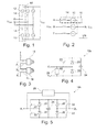
- Fig. 1 shows an indirect converter 10, which can convert a DC voltage U DC in an AC voltage U AC .
- the indirect converter 10 has two converter branches 12, which connect the inputs of the indirect converter 10, between which the voltage U DC is present, to an output, to which the voltage U AC is applied, via a respective throttle 14.
- the converter branches 12 each comprise a plurality of series-connected converter cells.
- the Indian Fig. 1 illustrated indirect converter 10 is designed to convert a phase of a current.
- These inverters have for each phase R, S, T an inverter 10 whose output each connected to one of the phases and whose inputs are connected to the inputs of the other inverters.
- the Fig. 2 shows a direct converter, which generates an output voltage UAC2 of frequency 2 from input voltages UAC1 of the three input phases R, S, T of frequency 1.
- the direct converter 16 is capable of connecting a phase voltage of U AC1 of a first frequency to a phase voltage of U AC2 .
- the direct converter 16 again has a converter branch 12, which connects the two inputs, at which the two voltages U AC1 and U AC2 , via a throttle 14. Accordingly, it is also possible to generate a plurality of output voltages UAC2 of frequency 2, for example for multiphase UAC2 systems. Accordingly, the output voltage UAC2 can also be kept close to 0 in order, for example, to realize reactive power compensation devices.
- an inverter branch 12 is shown from a plurality of converter cells 18.
- Each of the converter cells 18 has a first input X1 and a second input X2, which are connected either to the input or output of the converter branch 12 or to another converter cell 18.
- the converter cells 18 are connected in series via their inputs or outputs X1, X2.
- the Fig. 4 shows a unipolar inverter cell 18a, which in the indirect converter 10 from the Fig. 1 is used in the converter branches 12.
- the converter cell 18a has two freewheeling diodes 20, two power electronic switches 22, an energy store 24 in the form of a capacitor and a bridging unit 26.
- the power electronic switches 22 may be, for example, thyristors, IGCTs or IGBTs.
- the bypass unit 26 is connected in parallel to the other components of the converter cell 18a and connected to the inputs X1 and X2 of the converter cell 18a.
- the bypass unit 26 is a device that has a very low resistance in a first conductive state so that a current flows between the inputs X1 and X2 through the bypass unit 26 and not through the other structural components of the inverter cell 18a.
- a second non-conductive state in which the bridging unit 26 has a very high resistance, no or at least only a very small current can flow through the bridging element 26.
- the inverter cell 18a behaves as though the bridging unit 26 were not present.
- Fig. 5 shows a bipolar converter cell 18b, which is constructed in principle of two unipolar converter cells 18a, sharing the same energy storage 24.
- the bipolar converter cell 18b can be used in a direct converter 16.
- the bipolar converter cell 18b comprises four power electronic switches 22 and four freewheeling diodes 20.
- the power electronic switches 22 may be, for example, thyristors, IGCTs or IGBTs.
- the converter cell 18b also has a bridging unit 26 which is connected in parallel with the other components of the converter cell 18b in parallel with the inputs X1 and X2 of the converter cell 18b.
- the bridging element 26 has the same properties as the bridging element 26 from the Fig. 4 on.
- the incorporation of a small inductance between the unipolar or bipolar converter cell and the bridging element 26 may be provided.
- bipolar converter cell in a bipolar converter cell, two bridging units may be used, each connecting an external terminal (X1, X2) to the same terminal of the capacitor. Then the bipolar cell corresponds exactly to two unipolar cells connected at the two terminals of the capacitor.
- an inverter cell 18 which may be a unipolar inverter cell 18a or a bipolar converter cell 18b, is shown.
- the bridging unit 26 has two components connected in parallel to one another, a surge current element 28 and a redundancy element 30.
- the surge current element 28 provides the surge current capability of the converter cell 18. For example, in the case of various converter errors or external system errors, externally impressed surge currents must be briefly absorbed by the converter cell with the aid of the surge current element 28 via the inputs X1 and X2. In addition, cell-internal surge currents for protecting the redundancy elements can also be accommodated with the same protective element. This is possible, for example, to discharge the intermediate circuit with the capacitor 24, if, for example, in the unipolar converter cell 18 a from the Fig. 4 the power electronic switch 22 shown above is closed.
- the redundancy element 30 provides the redundancy capability of the inverter cell 18.
- a redundant capability of a converter cell can be understood as a permanent short circuit of the cell as a consequence of a cell malfunction.
- a bridging unit 26 is shown between the inputs and outputs X1 and X2 of a unipolar or bipolar converter cell 18, a smart, combined mechanical and power electronic bypass unit 26 is inserted which provides the controlled reduction of redundancy (failure of one or more inverter cells 18) as well as surge current capability in the event of external system faults can ensure.
- the bridging unit 26 comprises a combined mechanical-electrical bridging element 32 of a bistable mechanical relay 34 and a power electronic switch 36 comprising two antiparallel thyristors 38 or a triac.
- the power electronic switch 36 comprises a gate controller 40 or gate drive 40, which can switch the electronic switching elements 38, for example thyristors 38, via their gates.
- the combined mechanical-electrical bridging element 32 is driven by a control 42, the opening or closing signal via a first signal line 44 to the mechanical relay 34 and an opening or closing signal via a second signal line 46 to the gate controller 40 and thus can send to the power electronic switch 36.
- the control 42 and the components of the bridging element 32 that is, the relay 34, the gate controller 40 and the two thyristors 38 are powered by an energy store 48 with energy.
- the energy storage 48 is designed to provide enough energy to power the mechanical and power electronic bypass element 32 as well as its associated protective intelligence in the form of the driver 42 in the event of a fault.
- the energy store 48 is connected in parallel with the relay 34 and the two thyristors 36 to the inputs X1 and X2 of the converter cell 18 and can draw energy from the voltage applied to the converter cell 18 via these two inputs X1, X2. But it is also possible that the energy storage 48 draws energy from a power supply of the converter cell 18.
- the commercially available mechanical relays 34 connected to the outputs X1 and X2 can be operated out of specification with respect to the control voltage applied at the time of switch-on. This can be achieved that the switching time of the relay 34 is shortened.
- the relay 34 can be operated with respect to the switching voltage on the contacts outside the specification, as long as the functionally necessary isolation distances can be maintained.
- the relay 34 may be a commercially available bistable relay.
- the drive 42 is designed to implement external protection commands originating, for example, from a system protection unit 60 to evaluate local faults, such as an overvoltage, overcurrent or error message of the converter cell diagnosis 58.
- voltage measuring device 50 can be connected between the two inputs X1, X2 and / or an ammeter 52 in the input X1 and the input X2 be connected.
- the control 42 Via a signal line 54, the control 42, the current voltage U AC between the inputs X1 and X2 the voltage measuring device 50 and the signal line 56, the current I AC received from the ammeter 52.
- control 42 can receive opening and closing signals via a signal line 62 from a control and diagnostic unit 58 of the converter cell 18.
- the unit 58 may receive the values of voltage U AC , current I AC , voltage U DC and desaturation monitoring (in the case of IGBTs) or cell firing (in the case of IGCTs).
- the control 42 can optionally also send a switch-off signal to the controller 58 of the converter cell 18 via the signal line 62.
- the driver 42 receives open and close signals from a system protection unit 60 which monitors the entire inverter 10, 16 in which the converter cell 18 is installed.
- FIG. 10 shows a flowchart for a method by which the bypass unit 26 can protect the inverter cell 18.
- step S10 the voltage U AC and / or the current I AC between the two inputs X1, X2 of the converter cell 18 is determined.
- a step S12 the driver 42 determines whether a threshold value for the voltage U AC and / or the current I AC is exceeded. If this is the case, the control 42 decides to close the mechanical-electronic bridging element 32.
- the diagnostic unit 58 determines an internal error of the converter cell 18.
- the diagnostic unit 58 sends a closing signal to the driver 42.
- step S18 the system protection unit 60 detects an external or internal fault in the inverter 10, 16. The system protection unit 60 then sends a closing signal via the signal line 62 to the controller 42.
- steps S10 and S12, S14 and S16 as well as S18 and S20 may be performed alternatively to each other or simultaneously.
- a step S22 the driver 42, taking into account all information optionally sends a closing signal via the signal line 44 to the relay 34, which closes within milliseconds and a closing signal via the signal line 46 to the gate controller 40, then the two thyristors 38th converted into its conductive state.
- the thyristors become conductive within microseconds.
- diagnostic unit 58 or the system protection unit 60 detects that the internal error has been rectified or that the internal or external error of the converter 10, 16 is no longer present, they send an open signal to the controller 42, which then in one step S24 sends an open signal to the relay and / or the gate controller 40, whereupon the selected switching elements 34 and / or 36 are opened again and the bridging of the bridging element 26 is canceled if necessary.
- An external fault that may be detected by the system protection unit 60 may be, for example, a ground fault.
- a closing signal is sent to all the bypass units 26 of all the converter cells 18 of the converter 18. In these cases, it is advisable to close only the power electronic switch. As a result, all converter cells 18 of the converter are bridged by the bridging unit 26.
- the main breaker of the inverter 10, 16 are activated by the system protection unit 60.
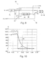
- Fig. 9 an embodiment of a part of a bridging unit 26 is shown.
- the outputs Y1 and Y2 in the Fig. 9 illustrated circuit 26 may include one or more bistable relays 34 and / or one or more gate controls 40 are driven for power electronic switches 36.
- the input U3 of the circuit 26 is connected to the input X1 of the converter cell 18, the input GND to the output X2 of the converter cell 18.
- the energy required for simultaneous switching (for example from one or more bistable relays 34 and / or one or more power electronic switches 36) is set in a capacitor C1 via the voltage or the capacitance.
- the energy store 48 comprises the capacitor C1.
- the circuit of Y1 via the capacitor C1 to the output Y2 to trigger the relay 34 and / or the gate control 40 is closed with a thyristor T1. This ensures that after an ignition pulse, the current from the capacitor C1 flows until the capacitor C1 is completely discharged or the circuit is interrupted.
- the energy for the energy storage C1 is either from the power supply belonging to the converter cell via the input U2 or via a series circuit of Transil or.
- the ignition of the thyristor T1 can be done either via too high a voltage at the input U3 or X1 of the circuit 26 or via a control input CTR.
- the charge and thus the voltage U1 on the capacitor C1 by integrated in the control unit 58, 60 power supply to the value held the voltage U2.
- the controller 58, 60 gives the command or the closing signal to bridge the converter cell 18
- the control terminal of the thyristor T1 is directly driven via the input CTR and thus the thyristor T1 is brought into the conducting state.
- the capacitor C1 is discharged via the connected bistable relays 34 and the gate controls 40, respectively.
- the voltage U1 is tapped across the capacitor C1 and via a series connection of Zener diodes 66 or Transil diodes 66 and a diac 68 to the control terminal of the thyristor T1 connected.
- Zener diodes 66 or Transil diodes 66 and a diac 68 to the control terminal of the thyristor T1 connected.
- Diac 68 changes its transmission characteristic so that the voltage drop across it decreases sharply. This increases the drive current for the thyristor T1 and adds triggering circuit 26 with hysteresis. This ensures that a single exceeding of the threshold voltage U1 reliably causes the triggering.
- the driver 42 includes elements 66, 68 and T1.
- the threshold voltage for charging the capacitor C1 can be adjusted.
- the threshold voltage of the block 66, 68 should be higher than the voltage U2, otherwise in normal operation, when the power supply unit of the connected converter cell 18 supplies the voltage U2, the ignition mechanism of the threshold circuit 26 is already set in motion.
- the Fig. 10 shows a diagram of voltage waveforms, which in a measurement at the bypass circuit 26 from the Fig. 9 were won.
- the time t in seconds is plotted to the right and the voltage in volts to the top.
- the capacitor voltage 72 is divided by 10.
- Graph 72 shows the voltage across capacitor C1, during which voltage U3 74 has been increased continuously, to a threshold voltage at which transistor chain 70 becomes conductive and charges capacitor C1 as soon as the threshold voltage for the thyristor T1 fires has been reached, the voltage U3 short-circuits and thus bypasses the converter cell 18.
Landscapes
- Engineering & Computer Science (AREA)
- Power Engineering (AREA)
- Inverter Devices (AREA)
- Power Conversion In General (AREA)
- Dc-Dc Converters (AREA)
Claims (11)
- Unité de pontage (26) pour court-circuiter une première (X1) et une deuxième (X2) entrée d'une cellule de convertisseur (18) d'un convertisseur (10) modulaire, comprenant :un relais mécanique bistable (34) ;un commutateur électronique de puissance (36) ;une commande (42) pour faire commuter le relais (34) etle commutateur électronique de puissance (36) ;le relais mécanique bistable (34) étant réalisé pour relier électriquement la première entrée (X1) avec la deuxième entrée (X2) ;le commutateur électronique de puissance (36) étant réalisé pour relier électriquement la première entrée (X1) avec la deuxième entrée (X2) ;un accumulateur d'énergie (48) étant prévu pour l'alimentation en énergie du relais mécanique (34), du commutateur électronique de puissance (36) et de la commande (42) ;la commande (42) comprenant un détecteur de surtension passif (70) et, en cas de dépassement de la surtension,l'accumulateur d'énergie (48) étant chargé par la surtension ;la commande (42) présentant un autre commutateur électronique (T1) qui est fermé lorsqu'une tension aux bornes de l'accumulateur d'énergie (48) dépasse une valeur prédéfinie, et la commande alimentant électriquement le relais bistable (34) et/ou le commutateur électronique de puissance (36) à partir de l'accumulateur d'énergie ; etla commande (42) présentant une hystérésis de sorte qu'en cas de franchissement vers le bas de la tension aux bornes de l'accumulateur d'énergie (48), le relais (34) et/ou le commutateur électronique de puissance (36) continuent d'être alimentés électriquement à partir de l'accumulateur d'énergie.
- Unité de pontage (26) selon la revendication 1, le commutateur électronique de puissance (36) étant réalisé de manière à se fermer en l'espace de quelques microsecondes à quelques dizaines de microsecondes et/ou
le relais mécanique bistable (34) étant réalisé de manière à se fermer en l'espace de quelques microsecondes à quelques dizaines de microsecondes. - Unité de pontage (26) selon la revendication 1 ou 2,
le commutateur électronique de puissance (36) comprenant deux thyristors (38) montés tête-bêche et/ou le commutateur électronique de puissance (36) comprenant un triac. - Unité de pontage (26) selon l'une des revendications précédentes,
la commande (42) étant réalisée pour recevoir un signal de fermeture ;
la commande (42) étant réalisée pour fermer le relais (34) et/ou le commutateur électronique de puissance (36) en réaction au signal de fermeture. - Unité de pontage (26) selon l'une des revendications précédentes,
la commande (42) étant réalisée pour recevoir un signal de réinitialisation ;
la commande (42) étant réalisée pour ouvrir le relais (34) et/ou le commutateur électronique de puissance (36) en réaction au signal de réinitialisation. - Unité de pontage (26) selon l'une des revendications précédentes,
la commande (42) étant réalisée pour déterminer une surtension et/ou une surintensité entre la première entrée (X1) et la deuxième entrée (X2) ;
la commande (42) étant réalisée pour fermer le relais (34) et/ou le commutateur électronique de puissance (36) lorsque la surtension et/ou la surintensité sont déterminées. - Unité de pontage (26) selon l'une des revendications précédentes,
la commande (42) étant réalisée pour détecter un signal de fermeture et/ou un signal de réinitialisation externe ;
la commande (42) étant réalisée pour fermer le relais (34) et/ou le commutateur électronique de puissance (36) lorsqu'un signal de fermeture externe a été détecté ;
la commande (42) étant réalisée pour ouvrir le relais (34) et/ou le commutateur électronique de puissance (36) lorsqu'un signal de réinitialisation externe a été détecté. - Cellule de convertisseur (18) comprenant :une unité de pontage (26) selon l'une des revendications 1 à 7.
- Cellule de convertisseur (18) selon la revendication 8, comprenant en outre :un dispositif de coupure sur surintensité (58) et/ou un dispositif de surveillance de désaturation d'un IGBT de la cellule de convertisseur (18) ;le dispositif de coupure sur surintensité (58) étant réalisé pour mettre hors circuit les composants semiconducteurs de la cellule de convertisseur (18) dans le cas d'une surintensité.
- Convertisseur (10) comprenant :une pluralité de cellules de convertisseur (18) selon la revendication 8 ou 9.
- Convertisseur (10) selon la revendication 10, comprenant en outre :une unité de protection du système ;l'unité de protection du système étant réalisée pour, en présence d'une erreur du convertisseur et/ou du système, fermer les commutateurs semiconducteurs de puissance des unités de pontage (26) des cellules de convertisseur (18) et, au choix, les réinitialiser après la correction du défaut.
Priority Applications (8)
| Application Number | Priority Date | Filing Date | Title |
|---|---|---|---|
| EP10157722A EP2369725B1 (fr) | 2010-03-25 | 2010-03-25 | Dispositif de court-circuit |
| CA2734911A CA2734911C (fr) | 2010-03-25 | 2011-03-23 | Unite de pont |
| KR1020110026569A KR101197066B1 (ko) | 2010-03-25 | 2011-03-24 | 브리징 유닛 |
| RU2011111203/28A RU2461912C1 (ru) | 2010-03-25 | 2011-03-24 | Шунтирующий модуль |
| US13/071,184 US8456786B2 (en) | 2010-03-25 | 2011-03-24 | Bridging unit |
| CN201110084784.7A CN102201728B (zh) | 2010-03-25 | 2011-03-25 | 桥接单元 |
| JP2011067555A JP5431398B2 (ja) | 2010-03-25 | 2011-03-25 | ブリッジングユニット |
| BRPI1100945-4A BRPI1100945A2 (pt) | 2010-03-25 | 2011-03-25 | célula conversora e unidade de ligação |
Applications Claiming Priority (1)
| Application Number | Priority Date | Filing Date | Title |
|---|---|---|---|
| EP10157722A EP2369725B1 (fr) | 2010-03-25 | 2010-03-25 | Dispositif de court-circuit |
Publications (2)
| Publication Number | Publication Date |
|---|---|
| EP2369725A1 EP2369725A1 (fr) | 2011-09-28 |
| EP2369725B1 true EP2369725B1 (fr) | 2012-09-26 |
Family
ID=42646807
Family Applications (1)
| Application Number | Title | Priority Date | Filing Date |
|---|---|---|---|
| EP10157722A Active EP2369725B1 (fr) | 2010-03-25 | 2010-03-25 | Dispositif de court-circuit |
Country Status (8)
| Country | Link |
|---|---|
| US (1) | US8456786B2 (fr) |
| EP (1) | EP2369725B1 (fr) |
| JP (1) | JP5431398B2 (fr) |
| KR (1) | KR101197066B1 (fr) |
| CN (1) | CN102201728B (fr) |
| BR (1) | BRPI1100945A2 (fr) |
| CA (1) | CA2734911C (fr) |
| RU (1) | RU2461912C1 (fr) |
Families Citing this family (47)
| Publication number | Priority date | Publication date | Assignee | Title |
|---|---|---|---|---|
| US8731765B2 (en) * | 2011-06-28 | 2014-05-20 | GM Global Technology Operations LLC | Method and apparatus for fault detection in a torque machine of a powertrain system |
| WO2013064310A1 (fr) | 2011-11-03 | 2013-05-10 | Abb Technology Ag | Circuit convertisseur et procédé permettant de faire fonctionner un tel circuit convertisseur |
| CN103107689A (zh) * | 2011-11-11 | 2013-05-15 | 台达电子企业管理(上海)有限公司 | 一种级联型变频器、功率单元及其旁路模块 |
| EP2595302A1 (fr) * | 2011-11-21 | 2013-05-22 | ABB Technology AG | Procédé et dispositif pour le maintien d'un module d'alimentation pendant l'operation d'un convertisseur multi-cellule modulaire |
| EP2597764B1 (fr) * | 2011-11-22 | 2016-04-13 | ABB Technology AG | Procédé de traitement des erreurs dans un convertisseur modulaire multiniveau et un tel convertisseur |
| KR101251166B1 (ko) * | 2011-12-12 | 2013-04-04 | 주식회사 효성 | 전력 변환 시스템의 모듈 스위칭 제어 장치 및 방법 |
| EP2608389A1 (fr) * | 2011-12-19 | 2013-06-26 | Siemens Aktiengesellschaft | Onduleur multiniveau avec une pluralité des sous-modules onduleur avec un dispositif de décharge central |
| EP2608344A1 (fr) | 2011-12-19 | 2013-06-26 | Siemens Aktiengesellschaft | Procédé de protection d'un condensateur de circuit intermédiaire dans un circuit de convertisseur |
| FR2987190B1 (fr) * | 2012-02-22 | 2014-06-27 | Inst Polytechnique Grenoble | Convertisseur de tension |
| KR101389579B1 (ko) * | 2012-12-28 | 2014-04-29 | 주식회사 효성 | 전력용 컨버터 |
| CN103236788B (zh) * | 2013-01-14 | 2015-03-25 | 燕山大学 | 自举式双输入直流变换器 |
| JP6009651B2 (ja) * | 2013-03-18 | 2016-10-19 | 三菱電機株式会社 | 電力変換装置 |
| EP2987229B1 (fr) * | 2013-04-18 | 2018-06-13 | ABB Schweiz AG | Bypass mecanique, bras d' onduleur et pont onduleur |
| CN103280989B (zh) * | 2013-05-15 | 2017-02-08 | 南京南瑞继保电气有限公司 | 一种换流器及其控制方法 |
| EP2824701B1 (fr) * | 2013-07-12 | 2020-05-06 | ABB Power Grids Switzerland AG | Dispositif semi-conducteur haute puissance |
| WO2015028665A2 (fr) * | 2013-08-30 | 2015-03-05 | Abb Technology Ag | Agencement de convertisseur |
| EP3745581B1 (fr) * | 2014-03-05 | 2022-11-30 | Mitsubishi Electric Corporation | Dispositif de conversion d'alimentation électrique |
| EP2921871B1 (fr) * | 2014-03-20 | 2020-02-05 | General Electric Technology GmbH | Procédé et dispositif de test d'intégrité de connexion pour convertisseurs de source de tension à plusieurs étages |
| CN104953609A (zh) * | 2014-03-27 | 2015-09-30 | 通用电气公司 | 直流电能传输系统和方法 |
| US9866120B2 (en) * | 2014-06-30 | 2018-01-09 | Mitsubishi Electric Corporation | Power conversion device |
| JP5730456B1 (ja) * | 2014-10-08 | 2015-06-10 | 三菱電機株式会社 | 電力変換装置 |
| CN104753367B (zh) * | 2015-03-06 | 2016-10-19 | 广东欧珀移动通信有限公司 | 电源适配器 |
| WO2016188589A1 (fr) * | 2015-05-28 | 2016-12-01 | Siemens Aktiengesellschaft | Module convertisseur commandé par tension |
| US10326355B2 (en) * | 2015-07-14 | 2019-06-18 | Mitsubishi Electric Corporation | Power conversion device |
| US9812946B2 (en) * | 2016-02-03 | 2017-11-07 | Delta Electronics, Inc. | Power converter and operating method thereof |
| EP3203621A1 (fr) * | 2016-02-03 | 2017-08-09 | Delta Electronics, Inc. | Convertisseur ca/cc modulaire multi-cellule avec connection ca en série et des commutateurs de dérivation |
| JP6455938B2 (ja) * | 2016-03-22 | 2019-01-23 | 東芝三菱電機産業システム株式会社 | 電力変換装置及びその制御方法 |
| WO2017168518A1 (fr) * | 2016-03-28 | 2017-10-05 | 三菱電機株式会社 | Dispositif de conversion de puissance |
| CN105896477A (zh) * | 2016-06-07 | 2016-08-24 | 南方电网科学研究院有限责任公司 | 一种模块化多电平换流器的接地保护方法及模块化多电平换流器 |
| US20170358567A1 (en) * | 2016-06-10 | 2017-12-14 | Littelfuse, Inc. | Transient suppressing circuit arrangements |
| CN106849016A (zh) * | 2017-01-23 | 2017-06-13 | 许继集团有限公司 | 一种mmc子模块故障保护方法及装置 |
| US10903757B2 (en) * | 2017-08-09 | 2021-01-26 | Siemens Aktiengesellschaft | Power module for a converter and multi-level converter |
| DE102017219499A1 (de) | 2017-11-02 | 2019-05-02 | Siemens Aktiengesellschaft | Elektrische Anordnung mit Teilmodulen sowie Teilmodule als solche |
| DE102018202661A1 (de) * | 2018-02-22 | 2019-08-22 | Zf Friedrichshafen Ag | Verfahren und Vorrichtung zum Entladen eines Zwischenkreiskondensators |
| US11463015B2 (en) * | 2018-05-17 | 2022-10-04 | Mitsubishi Electric Corporation | Power conversion apparatus |
| EP3621193A1 (fr) | 2018-09-06 | 2020-03-11 | ABB Schweiz AG | Fonction de mode de défaillance de court-circuit stable artificiel à l'aide de modules parallèles pour chaque fonction de commutation |
| EP3931957B1 (fr) * | 2019-02-28 | 2023-04-05 | Hitachi Energy Switzerland AG | Cellule de convertisseur avec protection en tension |
| EP3713074B1 (fr) * | 2019-03-21 | 2021-09-08 | General Electric Technology GmbH | Cellule de conversion pour un convertisseur de source de tension |
| UA141631U (uk) * | 2019-07-16 | 2020-04-27 | Дмитро Валерійович Хачатуров | Пристрій захисту силових комірок перетворювача частоти |
| CN110492757B (zh) * | 2019-08-13 | 2021-10-08 | 上海电机学院 | 一种背靠背变流器控制器 |
| KR102177141B1 (ko) | 2019-08-21 | 2020-11-10 | 효성중공업 주식회사 | 바이패스 스위치를 구비한 전력용 컨버터의 서브모듈 |
| KR102171603B1 (ko) | 2019-08-21 | 2020-10-29 | 효성중공업 주식회사 | 바이패스 스위치를 구비한 전력용 컨버터의 서브모듈 |
| WO2021083500A1 (fr) * | 2019-10-30 | 2021-05-06 | Abb Power Grids Switzerland Ag | Surveillance de l'état de dispositifs à semi-conducteur dans un convertisseur |
| JP7303139B2 (ja) * | 2020-03-06 | 2023-07-04 | 株式会社日立製作所 | 電力変換システム |
| EP3890178A1 (fr) * | 2020-04-02 | 2021-10-06 | General Electric Technology GmbH | Perfectionnements apportés ou se rapportant ou des convertisseurs chain-link |
| EP4007139B1 (fr) * | 2020-11-25 | 2023-04-05 | Hitachi Energy Switzerland AG | Module comprenant un dispositif de dérivation commutable |
| CN113472229B (zh) * | 2021-07-15 | 2024-04-26 | 昆明理工大学 | 一种具备直流故障清除和均压能力的混合桥臂拓扑结构 |
Family Cites Families (16)
| Publication number | Priority date | Publication date | Assignee | Title |
|---|---|---|---|---|
| DE1613718A1 (de) * | 1967-05-10 | 1970-07-23 | Bbc Brown Boveri & Cie | Stromrichteranordnung mit mindestens zwei auf ihrer Gleichstromseite in Reihe geschalteten Teilstromrichtern |
| JPS5161764A (ja) * | 1974-11-27 | 1976-05-28 | Hitachi Ltd | Handotaiseigyoseiryusoshino kadenatsuhogosochi |
| JPS6057293B2 (ja) * | 1977-05-26 | 1985-12-14 | 株式会社東芝 | 直流スイツチング回路の保護方式 |
| JPS5558773A (en) * | 1978-10-25 | 1980-05-01 | Mitsubishi Electric Corp | Overvoltage protector for thyristor |
| JPS6318967A (ja) * | 1986-07-11 | 1988-01-26 | Toshiba Corp | サイクロコンバ−タの制御装置 |
| SU1610491A1 (ru) * | 1988-11-10 | 1990-11-30 | Предприятие П/Я Р-6541 | Устройство дл шунтировани магнитной головки при сбо х электропитани |
| JPH02179219A (ja) * | 1988-12-28 | 1990-07-12 | Canon Inc | 電源装置 |
| JPH07177648A (ja) * | 1993-12-21 | 1995-07-14 | Toshiba Corp | 超電導応用装置の直流しゃ断システム |
| US5986909A (en) * | 1998-05-21 | 1999-11-16 | Robicon Corporation | Multiphase power supply with plural series connected cells and failed cell bypass |
| DE10323220B4 (de) | 2003-05-22 | 2014-07-17 | Siemens Aktiengesellschaft | Kurzschluss-Schaltung für einen Teilumrichter |
| US20060274468A1 (en) * | 2005-06-03 | 2006-12-07 | Phadke Vijay G | Active inrush current control using a relay for AC to DC converters |
| DE102005040543A1 (de) | 2005-08-26 | 2007-03-01 | Siemens Ag | Stromrichterschaltung mit verteilten Energiespeichern |
| CN101548461B (zh) * | 2006-12-08 | 2012-12-12 | 西门子公司 | 在电压中间电路变流器中用于控制直流侧的短路的半导体保护元件 |
| DE102007018344B4 (de) | 2007-04-16 | 2022-08-04 | Siemens Energy Global GmbH & Co. KG | Vorrichtung zum Schutz von Umrichtermodulen |
| KR20100115742A (ko) | 2008-01-22 | 2010-10-28 | 지멘스 악티엔게젤샤프트 | 불꽃 점화식 개시 수단을 구비한 단락 장치 |
| JP2010119239A (ja) * | 2008-11-13 | 2010-05-27 | Mitsubishi Heavy Ind Ltd | Smes装置、smes用インターフェース装置及びその駆動方法 |
-
2010
- 2010-03-25 EP EP10157722A patent/EP2369725B1/fr active Active
-
2011
- 2011-03-23 CA CA2734911A patent/CA2734911C/fr active Active
- 2011-03-24 RU RU2011111203/28A patent/RU2461912C1/ru not_active IP Right Cessation
- 2011-03-24 US US13/071,184 patent/US8456786B2/en active Active
- 2011-03-24 KR KR1020110026569A patent/KR101197066B1/ko not_active IP Right Cessation
- 2011-03-25 JP JP2011067555A patent/JP5431398B2/ja not_active Expired - Fee Related
- 2011-03-25 BR BRPI1100945-4A patent/BRPI1100945A2/pt not_active IP Right Cessation
- 2011-03-25 CN CN201110084784.7A patent/CN102201728B/zh active Active
Also Published As
| Publication number | Publication date |
|---|---|
| CA2734911C (fr) | 2014-05-06 |
| US20110235221A1 (en) | 2011-09-29 |
| KR101197066B1 (ko) | 2012-11-06 |
| CN102201728B (zh) | 2014-10-29 |
| CA2734911A1 (fr) | 2011-09-25 |
| RU2461912C1 (ru) | 2012-09-20 |
| EP2369725A1 (fr) | 2011-09-28 |
| JP5431398B2 (ja) | 2014-03-05 |
| US8456786B2 (en) | 2013-06-04 |
| KR20110107767A (ko) | 2011-10-04 |
| CN102201728A (zh) | 2011-09-28 |
| JP2011205887A (ja) | 2011-10-13 |
| BRPI1100945A2 (pt) | 2012-12-18 |
Similar Documents
| Publication | Publication Date | Title |
|---|---|---|
| EP2369725B1 (fr) | Dispositif de court-circuit | |
| EP2597764B1 (fr) | Procédé de traitement des erreurs dans un convertisseur modulaire multiniveau et un tel convertisseur | |
| DE102013110240B4 (de) | Schaltungsanordnung für einen Photovoltaikwechselrichter zur Ausschaltentlastung mit Kurzschlussschaltern und Verwendungen der Schaltungsanordnung | |
| EP3583695B1 (fr) | Procédé de commande d'un commutateur à courant continu, commutateur à courant continu et système de tension continue | |
| DE112017000286T5 (de) | Leistungsumrichtvorrichtung | |
| EP2810289B1 (fr) | Procédé de commutation d'un tronçon de réseaux de tension continue au moyen d'un interrupteur de tension continue | |
| WO2008110129A1 (fr) | Procédé pour limiter les dommages à un redresseur présentant un semi-conducteur de puissance dans le cas d'un court-circuit dans un circuit intermédiaire à tension continue | |
| DE102010007452A1 (de) | Schaltentlastung für einen Trennschalter | |
| EP2282388A1 (fr) | Dispositif d'alimentation en énergie électrique d'une multitude de chaînes de modules photovoltaïques dans un réseau électrique | |
| DE112016001334T5 (de) | Gleichstromwandler | |
| DE102012109012B4 (de) | Schaltungsanordnung für ein Solarkraftwerk mit einer Gleichspannungsquelle für eine Offsetspannung | |
| DE19600547A1 (de) | Umrichterschutzgerät für elektrisches Netz | |
| EP3259827B1 (fr) | Installation de remplacement de réseau, système de mise à la terre pour une installation de remplacement de réseau et procédé de fonctionnement | |
| DE102015107718B4 (de) | Vorrichtung und Verfahren zum Absichern einer Bordnetz-Komponente eines Fahrzeug-Bordnetzes | |
| WO2014060181A1 (fr) | Agencement de circuit de protection pour un réseau multitension | |
| DE102010053942A1 (de) | Abschalt- und Überbrückungsschaltung für ein Fahrzeug, insbesondere Elektrofahrzeug, umfassend eine Batterie mit Zellen, sowie Fahrzeug damit und Verfahren zum Ansteuern einer solchen | |
| DE102018119916A1 (de) | Elektrische AC/DC-Umwandlungs-Anordnung | |
| EP3783783A1 (fr) | Agencement de régulation d'un flux de puissance dans un réseau à tension alternative et procédé de protection de l'agencement | |
| DE10348162B3 (de) | Vorrichtung zur redundanten Energieversorgung sicherheitsrelevanter Verbraucher | |
| EP2926455B1 (fr) | Dispositif d'interruption de courants continus dans des branches de dérivation d'un noeud de réseau de tension continue | |
| DE102019215790B4 (de) | Steuergeräteschaltung für ein Kraftfahrzeug sowie Kraftfahrzeug und Betriebsverfahren für die Steuergeräteschaltung | |
| DE102021202914B3 (de) | Pulswechselrichteranordnung und Verfahren zum Betreiben einer Pulswechselrichteranordnung | |
| EP2904677B1 (fr) | Circuiterie comprenant un onduleur | |
| DE102011053728A9 (de) | Batteriesystem und Verfahren zum Abschalten von in Serie geschalteten Energiespeichermodulen einer Batterie eines Batteriesystems | |
| DE102020116974A1 (de) | Leistungsschalter für Gleichströme |
Legal Events
| Date | Code | Title | Description |
|---|---|---|---|
| PUAI | Public reference made under article 153(3) epc to a published international application that has entered the european phase |
Free format text: ORIGINAL CODE: 0009012 |
|
| AK | Designated contracting states |
Kind code of ref document: A1 Designated state(s): AT BE BG CH CY CZ DE DK EE ES FI FR GB GR HR HU IE IS IT LI LT LU LV MC MK MT NL NO PL PT RO SE SI SK SM TR |
|
| 17P | Request for examination filed |
Effective date: 20120319 |
|
| GRAP | Despatch of communication of intention to grant a patent |
Free format text: ORIGINAL CODE: EPIDOSNIGR1 |
|
| GRAS | Grant fee paid |
Free format text: ORIGINAL CODE: EPIDOSNIGR3 |
|
| GRAA | (expected) grant |
Free format text: ORIGINAL CODE: 0009210 |
|
| AK | Designated contracting states |
Kind code of ref document: B1 Designated state(s): AT BE BG CH CY CZ DE DK EE ES FI FR GB GR HR HU IE IS IT LI LT LU LV MC MK MT NL NO PL PT RO SE SI SK SM TR |
|
| REG | Reference to a national code |
Ref country code: GB Ref legal event code: FG4D Free format text: NOT ENGLISH |
|
| REG | Reference to a national code |
Ref country code: CH Ref legal event code: EP |
|
| REG | Reference to a national code |
Ref country code: AT Ref legal event code: REF Ref document number: 577416 Country of ref document: AT Kind code of ref document: T Effective date: 20121015 |
|
| REG | Reference to a national code |
Ref country code: IE Ref legal event code: FG4D Free format text: LANGUAGE OF EP DOCUMENT: GERMAN |
|
| REG | Reference to a national code |
Ref country code: DE Ref legal event code: R096 Ref document number: 502010001334 Country of ref document: DE Effective date: 20121122 |
|
| PG25 | Lapsed in a contracting state [announced via postgrant information from national office to epo] |
Ref country code: NO Free format text: LAPSE BECAUSE OF FAILURE TO SUBMIT A TRANSLATION OF THE DESCRIPTION OR TO PAY THE FEE WITHIN THE PRESCRIBED TIME-LIMIT Effective date: 20121226 Ref country code: FI Free format text: LAPSE BECAUSE OF FAILURE TO SUBMIT A TRANSLATION OF THE DESCRIPTION OR TO PAY THE FEE WITHIN THE PRESCRIBED TIME-LIMIT Effective date: 20120926 Ref country code: HR Free format text: LAPSE BECAUSE OF FAILURE TO SUBMIT A TRANSLATION OF THE DESCRIPTION OR TO PAY THE FEE WITHIN THE PRESCRIBED TIME-LIMIT Effective date: 20120926 Ref country code: LT Free format text: LAPSE BECAUSE OF FAILURE TO SUBMIT A TRANSLATION OF THE DESCRIPTION OR TO PAY THE FEE WITHIN THE PRESCRIBED TIME-LIMIT Effective date: 20120926 |
|
| REG | Reference to a national code |
Ref country code: LT Ref legal event code: MG4D Effective date: 20120926 |
|
| REG | Reference to a national code |
Ref country code: NL Ref legal event code: VDEP Effective date: 20120926 |
|
| PG25 | Lapsed in a contracting state [announced via postgrant information from national office to epo] |
Ref country code: SI Free format text: LAPSE BECAUSE OF FAILURE TO SUBMIT A TRANSLATION OF THE DESCRIPTION OR TO PAY THE FEE WITHIN THE PRESCRIBED TIME-LIMIT Effective date: 20120926 Ref country code: LV Free format text: LAPSE BECAUSE OF FAILURE TO SUBMIT A TRANSLATION OF THE DESCRIPTION OR TO PAY THE FEE WITHIN THE PRESCRIBED TIME-LIMIT Effective date: 20120926 Ref country code: SE Free format text: LAPSE BECAUSE OF FAILURE TO SUBMIT A TRANSLATION OF THE DESCRIPTION OR TO PAY THE FEE WITHIN THE PRESCRIBED TIME-LIMIT Effective date: 20120926 Ref country code: GR Free format text: LAPSE BECAUSE OF FAILURE TO SUBMIT A TRANSLATION OF THE DESCRIPTION OR TO PAY THE FEE WITHIN THE PRESCRIBED TIME-LIMIT Effective date: 20121227 |
|
| PG25 | Lapsed in a contracting state [announced via postgrant information from national office to epo] |
Ref country code: NL Free format text: LAPSE BECAUSE OF FAILURE TO SUBMIT A TRANSLATION OF THE DESCRIPTION OR TO PAY THE FEE WITHIN THE PRESCRIBED TIME-LIMIT Effective date: 20120926 Ref country code: CZ Free format text: LAPSE BECAUSE OF FAILURE TO SUBMIT A TRANSLATION OF THE DESCRIPTION OR TO PAY THE FEE WITHIN THE PRESCRIBED TIME-LIMIT Effective date: 20120926 Ref country code: IS Free format text: LAPSE BECAUSE OF FAILURE TO SUBMIT A TRANSLATION OF THE DESCRIPTION OR TO PAY THE FEE WITHIN THE PRESCRIBED TIME-LIMIT Effective date: 20130126 Ref country code: EE Free format text: LAPSE BECAUSE OF FAILURE TO SUBMIT A TRANSLATION OF THE DESCRIPTION OR TO PAY THE FEE WITHIN THE PRESCRIBED TIME-LIMIT Effective date: 20120926 Ref country code: RO Free format text: LAPSE BECAUSE OF FAILURE TO SUBMIT A TRANSLATION OF THE DESCRIPTION OR TO PAY THE FEE WITHIN THE PRESCRIBED TIME-LIMIT Effective date: 20120926 |
|
| PG25 | Lapsed in a contracting state [announced via postgrant information from national office to epo] |
Ref country code: PT Free format text: LAPSE BECAUSE OF FAILURE TO SUBMIT A TRANSLATION OF THE DESCRIPTION OR TO PAY THE FEE WITHIN THE PRESCRIBED TIME-LIMIT Effective date: 20130128 Ref country code: SK Free format text: LAPSE BECAUSE OF FAILURE TO SUBMIT A TRANSLATION OF THE DESCRIPTION OR TO PAY THE FEE WITHIN THE PRESCRIBED TIME-LIMIT Effective date: 20120926 Ref country code: PL Free format text: LAPSE BECAUSE OF FAILURE TO SUBMIT A TRANSLATION OF THE DESCRIPTION OR TO PAY THE FEE WITHIN THE PRESCRIBED TIME-LIMIT Effective date: 20120926 |
|
| PG25 | Lapsed in a contracting state [announced via postgrant information from national office to epo] |
Ref country code: DK Free format text: LAPSE BECAUSE OF FAILURE TO SUBMIT A TRANSLATION OF THE DESCRIPTION OR TO PAY THE FEE WITHIN THE PRESCRIBED TIME-LIMIT Effective date: 20120926 Ref country code: BG Free format text: LAPSE BECAUSE OF FAILURE TO SUBMIT A TRANSLATION OF THE DESCRIPTION OR TO PAY THE FEE WITHIN THE PRESCRIBED TIME-LIMIT Effective date: 20121226 |
|
| PLBE | No opposition filed within time limit |
Free format text: ORIGINAL CODE: 0009261 |
|
| STAA | Information on the status of an ep patent application or granted ep patent |
Free format text: STATUS: NO OPPOSITION FILED WITHIN TIME LIMIT |
|
| 26N | No opposition filed |
Effective date: 20130627 |
|
| BERE | Be: lapsed |
Owner name: ABB SCHWEIZ A.G. Effective date: 20130331 |
|
| REG | Reference to a national code |
Ref country code: DE Ref legal event code: R097 Ref document number: 502010001334 Country of ref document: DE Effective date: 20130627 |
|
| PG25 | Lapsed in a contracting state [announced via postgrant information from national office to epo] |
Ref country code: MC Free format text: LAPSE BECAUSE OF NON-PAYMENT OF DUE FEES Effective date: 20130331 Ref country code: ES Free format text: LAPSE BECAUSE OF FAILURE TO SUBMIT A TRANSLATION OF THE DESCRIPTION OR TO PAY THE FEE WITHIN THE PRESCRIBED TIME-LIMIT Effective date: 20130106 |
|
| PG25 | Lapsed in a contracting state [announced via postgrant information from national office to epo] |
Ref country code: CY Free format text: LAPSE BECAUSE OF FAILURE TO SUBMIT A TRANSLATION OF THE DESCRIPTION OR TO PAY THE FEE WITHIN THE PRESCRIBED TIME-LIMIT Effective date: 20120926 |
|
| REG | Reference to a national code |
Ref country code: IE Ref legal event code: MM4A |
|
| PG25 | Lapsed in a contracting state [announced via postgrant information from national office to epo] |
Ref country code: IE Free format text: LAPSE BECAUSE OF NON-PAYMENT OF DUE FEES Effective date: 20130325 Ref country code: BE Free format text: LAPSE BECAUSE OF NON-PAYMENT OF DUE FEES Effective date: 20130331 |
|
| PG25 | Lapsed in a contracting state [announced via postgrant information from national office to epo] |
Ref country code: MT Free format text: LAPSE BECAUSE OF FAILURE TO SUBMIT A TRANSLATION OF THE DESCRIPTION OR TO PAY THE FEE WITHIN THE PRESCRIBED TIME-LIMIT Effective date: 20120926 |
|
| PG25 | Lapsed in a contracting state [announced via postgrant information from national office to epo] |
Ref country code: SM Free format text: LAPSE BECAUSE OF FAILURE TO SUBMIT A TRANSLATION OF THE DESCRIPTION OR TO PAY THE FEE WITHIN THE PRESCRIBED TIME-LIMIT Effective date: 20120926 |
|
| PG25 | Lapsed in a contracting state [announced via postgrant information from national office to epo] |
Ref country code: TR Free format text: LAPSE BECAUSE OF FAILURE TO SUBMIT A TRANSLATION OF THE DESCRIPTION OR TO PAY THE FEE WITHIN THE PRESCRIBED TIME-LIMIT Effective date: 20120926 |
|
| PG25 | Lapsed in a contracting state [announced via postgrant information from national office to epo] |
Ref country code: MK Free format text: LAPSE BECAUSE OF FAILURE TO SUBMIT A TRANSLATION OF THE DESCRIPTION OR TO PAY THE FEE WITHIN THE PRESCRIBED TIME-LIMIT Effective date: 20120926 Ref country code: HU Free format text: LAPSE BECAUSE OF FAILURE TO SUBMIT A TRANSLATION OF THE DESCRIPTION OR TO PAY THE FEE WITHIN THE PRESCRIBED TIME-LIMIT; INVALID AB INITIO Effective date: 20100325 Ref country code: LU Free format text: LAPSE BECAUSE OF NON-PAYMENT OF DUE FEES Effective date: 20130325 |
|
| REG | Reference to a national code |
Ref country code: FR Ref legal event code: PLFP Year of fee payment: 7 |
|
| REG | Reference to a national code |
Ref country code: AT Ref legal event code: MM01 Ref document number: 577416 Country of ref document: AT Kind code of ref document: T Effective date: 20150325 |
|
| PG25 | Lapsed in a contracting state [announced via postgrant information from national office to epo] |
Ref country code: AT Free format text: LAPSE BECAUSE OF NON-PAYMENT OF DUE FEES Effective date: 20150325 |
|
| PGFP | Annual fee paid to national office [announced via postgrant information from national office to epo] |
Ref country code: IT Payment date: 20160324 Year of fee payment: 7 |
|
| REG | Reference to a national code |
Ref country code: FR Ref legal event code: PLFP Year of fee payment: 8 |
|
| PG25 | Lapsed in a contracting state [announced via postgrant information from national office to epo] |
Ref country code: IT Free format text: LAPSE BECAUSE OF NON-PAYMENT OF DUE FEES Effective date: 20170325 |
|
| REG | Reference to a national code |
Ref country code: FR Ref legal event code: PLFP Year of fee payment: 9 |
|
| REG | Reference to a national code |
Ref country code: DE Ref legal event code: R084 Ref document number: 502010001334 Country of ref document: DE |
|
| REG | Reference to a national code |
Ref country code: CH Ref legal event code: NV Representative=s name: DENNEMEYER AG, CH Ref country code: CH Ref legal event code: PUE Owner name: ABB POWER GRIDS SWITZERLAND AG, CH Free format text: FORMER OWNER: ABB SCHWEIZ AG, CH |
|
| REG | Reference to a national code |
Ref country code: DE Ref legal event code: R081 Ref document number: 502010001334 Country of ref document: DE Owner name: HITACHI ENERGY SWITZERLAND AG, CH Free format text: FORMER OWNER: ABB SCHWEIZ AG, BADEN, CH Ref country code: DE Ref legal event code: R081 Ref document number: 502010001334 Country of ref document: DE Owner name: HITACHI ENERGY LTD, CH Free format text: FORMER OWNER: ABB SCHWEIZ AG, BADEN, CH Ref country code: DE Ref legal event code: R082 Ref document number: 502010001334 Country of ref document: DE Representative=s name: DENNEMEYER & ASSOCIATES S.A., DE Ref country code: DE Ref legal event code: R081 Ref document number: 502010001334 Country of ref document: DE Owner name: ABB POWER GRIDS SWITZERLAND AG, CH Free format text: FORMER OWNER: ABB SCHWEIZ AG, BADEN, CH |
|
| REG | Reference to a national code |
Ref country code: GB Ref legal event code: 732E Free format text: REGISTERED BETWEEN 20211104 AND 20211110 |
|
| REG | Reference to a national code |
Ref country code: DE Ref legal event code: R081 Ref document number: 502010001334 Country of ref document: DE Owner name: HITACHI ENERGY SWITZERLAND AG, CH Free format text: FORMER OWNER: ABB POWER GRIDS SWITZERLAND AG, BADEN, CH Ref country code: DE Ref legal event code: R081 Ref document number: 502010001334 Country of ref document: DE Owner name: HITACHI ENERGY LTD, CH Free format text: FORMER OWNER: ABB POWER GRIDS SWITZERLAND AG, BADEN, CH |
|
| P01 | Opt-out of the competence of the unified patent court (upc) registered |
Effective date: 20230527 |
|
| REG | Reference to a national code |
Ref country code: DE Ref legal event code: R082 Ref document number: 502010001334 Country of ref document: DE Representative=s name: DENNEMEYER & ASSOCIATES S.A., DE Ref country code: DE Ref legal event code: R081 Ref document number: 502010001334 Country of ref document: DE Owner name: HITACHI ENERGY LTD, CH Free format text: FORMER OWNER: HITACHI ENERGY SWITZERLAND AG, BADEN, CH |
|
| PGFP | Annual fee paid to national office [announced via postgrant information from national office to epo] |
Ref country code: DE Payment date: 20240320 Year of fee payment: 15 Ref country code: GB Payment date: 20240320 Year of fee payment: 15 |
|
| PGFP | Annual fee paid to national office [announced via postgrant information from national office to epo] |
Ref country code: FR Payment date: 20240322 Year of fee payment: 15 |
|
| PGFP | Annual fee paid to national office [announced via postgrant information from national office to epo] |
Ref country code: CH Payment date: 20240401 Year of fee payment: 15 |
|
| REG | Reference to a national code |
Ref country code: GB Ref legal event code: 732E Free format text: REGISTERED BETWEEN 20240718 AND 20240724 |