EP2367275B2 - Nicht isolierte Gleichspannungswandler für ein Solarkraftwerk - Google Patents
Nicht isolierte Gleichspannungswandler für ein Solarkraftwerk Download PDFInfo
- Publication number
- EP2367275B2 EP2367275B2 EP10156854.1A EP10156854A EP2367275B2 EP 2367275 B2 EP2367275 B2 EP 2367275B2 EP 10156854 A EP10156854 A EP 10156854A EP 2367275 B2 EP2367275 B2 EP 2367275B2
- Authority
- EP
- European Patent Office
- Prior art keywords
- switch
- converter
- isolated
- diode
- voltage
- Prior art date
- Legal status (The legal status is an assumption and is not a legal conclusion. Google has not performed a legal analysis and makes no representation as to the accuracy of the status listed.)
- Not-in-force
Links
Images
Classifications
-
- H—ELECTRICITY
- H02—GENERATION; CONVERSION OR DISTRIBUTION OF ELECTRIC POWER
- H02M—APPARATUS FOR CONVERSION BETWEEN AC AND AC, BETWEEN AC AND DC, OR BETWEEN DC AND DC, AND FOR USE WITH MAINS OR SIMILAR POWER SUPPLY SYSTEMS; CONVERSION OF DC OR AC INPUT POWER INTO SURGE OUTPUT POWER; CONTROL OR REGULATION THEREOF
- H02M3/00—Conversion of dc power input into dc power output
- H02M3/02—Conversion of dc power input into dc power output without intermediate conversion into ac
- H02M3/04—Conversion of dc power input into dc power output without intermediate conversion into ac by static converters
- H02M3/10—Conversion of dc power input into dc power output without intermediate conversion into ac by static converters using discharge tubes with control electrode or semiconductor devices with control electrode
- H02M3/145—Conversion of dc power input into dc power output without intermediate conversion into ac by static converters using discharge tubes with control electrode or semiconductor devices with control electrode using devices of a triode or transistor type requiring continuous application of a control signal
- H02M3/155—Conversion of dc power input into dc power output without intermediate conversion into ac by static converters using discharge tubes with control electrode or semiconductor devices with control electrode using devices of a triode or transistor type requiring continuous application of a control signal using semiconductor devices only
- H02M3/156—Conversion of dc power input into dc power output without intermediate conversion into ac by static converters using discharge tubes with control electrode or semiconductor devices with control electrode using devices of a triode or transistor type requiring continuous application of a control signal using semiconductor devices only with automatic control of output voltage or current, e.g. switching regulators
- H02M3/158—Conversion of dc power input into dc power output without intermediate conversion into ac by static converters using discharge tubes with control electrode or semiconductor devices with control electrode using devices of a triode or transistor type requiring continuous application of a control signal using semiconductor devices only with automatic control of output voltage or current, e.g. switching regulators including plural semiconductor devices as final control devices for a single load
Definitions
- the present invention relates to an electronic power converter, and more particularly to a non-isolated DC - DC converter.
- An object of the present invention is thus to provide a non-isolated DC - DC converter that allows using a full-bridge inverter for the interface to the electrical network to be supplied.
- This object of the invention is achieved by a non-isolated DC - DC converter which is characterized by what is stated in the independent claim 1.
- the preferred embodiments of the invention are disclosed in the dependent claims.
- An advantage of the non-isolated DC - DC converter of the invention is that it can be connected to an electrical network to be supplied through a full-bridge inverter. Another advantage is that the non-isolated DC - DC converter of the invention include a buck-boost characteristic that allows using components with lower blocking voltage in an inverter connected between the non-isolated DC - DC converter and an electrical network to be supplied. Further advantage of the non-isolated DC - DC converter of the invention is that it allows, when connected to an electrical network to be supplied through a full-bridge inverter, reducing an inductance of a filter between the inverter and the electrical network when operating with a three-level modulation.
- an electronic power converter system comprising a non-isolated DC - DC converter of the invention and a full-bridge inverter allows to ground at the same time the negative input terminal of the DC - DC converter and an electrical network fed by the full-bridge inverter.
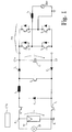
- FIG. 1 shows a connecting diagram of a solar power plant comprising a non-isolated DC - DC converter according to an embodiment of the invention.
- the solar power plant shown in Figure 1 comprises photovoltaic cell means PV connected to an electrical network ENW through an electronic power converter system comprising a non-isolated DC - DC converter and a full-bridge inverter FIB.
- the photovoltaic cell means PV are adapted to convert solar energy into direct current.
- the non-isolated DC - DC converter has a positive input terminal IT+, a negative input terminal IT-, a positive output terminal OT+, and a negative output terminal OT-.
- the negative input terminal IT- is grounded.
- the non-isolated DC - DC converter is adapted to convert an input DC voltage u in present between the positive input terminal IT+ and the negative input terminal IT- into a converted DC voltage u 1 present between the positive output terminal OT+ and the negative output terminal OT-.
- the non-isolated DC - DC converter comprises a first switch S 1 , a second switch S 2 , a third switch S 3 , a first diode D 1 , a second diode D 2 , a third diode D 3 , a first inductor L 1 and a first capacitor C 1 .
- the non-isolated DC - DC converter further comprises control means CTRL adapted to control each of the first switch S 1 , the second switch S 2 , and the third switch S 3 selectively into a closed state or into an open state, the closed state being a conductive state and the open state being a non-conductive state.
- the first switch S 1 , the second switch S 2 and the third switch S 3 may be for example IGBTs or MOSFETs.
- the first switch S 1 , the first inductor L 1 and the second diode D 2 are connected in series between the positive input terminal IT+ and the positive output terminal OT+ such that the first inductor L 1 is connected between the first switch S 1 and the anode of the second diode D 2 , the cathode of the second diode D 2 facing the positive output terminal OT+.
- the second switch S 2 and the third diode D 3 are connected in series between the negative input terminal IT- and the negative output terminal OT- such that the cathode of the third diode D 3 is facing the second switch S 2 , and the anode of the third diode D 3 is facing the negative output terminal OT-.
- the cathode of the first diode D 1 is connected between the first switch S 1 and the first inductor L 1
- the anode of the first diode D 1 is connected between the second switch S 2 and the cathode of the third diode D 3
- the third switch S 3 is connected between a point located between the first inductor L 1 and the anode of the second diode D 2 , and a point located between the second switch S 2 and the cathode of the third diode D 3
- the first capacitor C 1 is connected between the cathode of the second diode D 2 and the anode of the third diode D 3 .
- the control means CTRL are adapted to provide: a first switching stage where the first switch S 1 , the second switch S 2 and the third switch S 3 are in a closed state, a second switching stage where the first switch S 1 , the second switch S 2 and the third switch S 3 are in an open state, and a converting operation by alternating between the first switching stage and the second switching stage.
- the photovoltaic cell means PV are conductively connected to the first inductor L 1 allowing a current to flow between the photovoltaic cell means PV and the first inductor L 1 , wherein energy is transferred from the photovoltaic cell means PV into the first inductor L 1 .
- the first inductor L 1 is conductively connected to the first capacitor C 1 , allowing a current to flow between the first inductor L 1 and the first capacitor C 1 , wherein energy is transferred from the first inductor L 1 into the first capacitor C 1 .
- the first capacitor C 1 is never directly connected to the photovoltaic cell means PV. In other words, during operation of the non-isolated DC - DC converter a current flowing between the positive input terminal IT+ and the negative input terminal IT- never flows through the first capacitor C 1 . Consequently, the first capacitor C 1 is a floating capacitor.
- the control means CTRL are adapted to regulate, during the converting operation, the converted DC voltage u 1 by adjusting the ratio of duration of the first switching stages to duration of the second switching stages. Since the first switch S 1 , the second switch S 2 and the third switch S 3 are opened and closed simultaneously, they have a common duty cycle.
- Equation ⁇ 1 ⁇ ⁇ 1 is the duration of the first switching stage
- T c is the cycle time.
- the common duty cycle DS is the proportion of time during which the controllable switches S 1 to S 3 are in the closed state.
- adjusting the ratio of duration of the first switching stages to duration of the second switching stages means adjusting the duty-cycle DS of the first switch S 1 , the second switch S 2 and the third switch S 3 .
- Equation ⁇ 3 ⁇ shows that the non-isolated DC - DC converter is able to boost or buck the input DC voltage u in .
- Boosting a DC voltage means increasing the magnitude of the DC voltage
- bucking a DC voltage means decreasing the magnitude of the DC voltage.
- the non-isolated DC - DC converter depicted in Figure 1 further comprises an input voltage sensor SR IN adapted to determine a magnitude of the input DC voltage u in .
- the control means CTRL are communicatively connected to the input voltage sensor SR IN for receiving data relating to the magnitude of the input DC voltage u in .
- the control means CTRL are adapted to adjust the ratio of duration of the first switching stages to duration of the second switching stages responsive to the data relating to the magnitude of the input DC voltage u in .
- the full-bridge inverter FIB comprises four switches denoted with S 4 , S 5 , S 6 , and S 7 .
- the full-bridge inverter FIB is connected to the electrical network ENW through a second inductor L 2 , which acts as a filter inductor.
- the electrical network ENW is grounded.
- the full-bridge inverter FIB may be operated with a three-level modulation, and therefore the rating of the second inductor L 2 may be reduced compared with the rating required when using a half-bridge inverter.
- the full-bridge inverter FIB When operated with a three-level modulation, the full-bridge inverter FIB is able to apply to the electrical network ENW a voltage +u 1 by closing switches S 4 and S 7 , a voltage -u 1 by closing switches S 5 and S 6 , and a zero voltage by closing switches S 4 and S 5 .
- Non-isolated DC - DC converter is not limited to a solar power plant.
- the photovoltaic cell means of a solar power plant may be replaced with a different type of power supply having a positive supply terminal and a negative supply terminal, the power supply being adapted to generate a direct current and to feed the direct current out of the power supply via the positive and negative supply terminals.
Claims (10)
- Convertisseur DC-DC non-isolé pour une centrale solaire, le convertisseur DC-DC non-isolé comprenant une borne d'entrée positive (IT+), une borne d'entrée négative (IT-), une borne de sortie positive (OT+) et une borne de sortie négative (OT-), le convertisseur DC-DC non-isolé étant adapté pour convertir une tension DC d'entrée (uin) présente entre la borne d'entrée positive (IT+) et la borne d'entrée négative (IT-) en une tension DC convertie (u1) présente entre la borne de sortie positive (OT+) et la borne de sortie négative (OT-), le convertisseur DC-DC non-isolé comprenant un premier commutateur (S1), un deuxième commutateur (S2), un troisième commutateur (S3), une première diode (D1), une deuxième diode (D2), une troisième diode (D3), un premier inducteur (L1) et un premier condensateur (C1) ;
le premier commutateur (S1), le premier inducteur (L1) et la deuxième diode (D2) étant reliés en série entre la borne d'entrée positive (IT+) et la borne de sortie positive (OT+) de sorte que le premier inducteur (L1) soit relié entre le premier commutateur (S1) et l'anode de la deuxième diode (D2), la cathode de la deuxième diode (D2) étant tournée vers la borne de sortie positive (OT+);
le deuxième commutateur (S2) et la troisième diode (D3) étant reliés en série entre la borne d'entrée négative (IT-) et la borne de sortie négative (OT-) de sorte que la cathode de la troisième diode (D3) soit tournée vers le deuxième commutateur (S2) et que l'anode de la troisième diode (D3) soit tournée vers la borne de sortie négative (OT-) ;
la cathode de la première diode (D1) étant reliée entre le premier commutateur (S1) et le premier inducteur (L1), caractérisé en ce que
l'anode de la première diode (D1) est reliée entre le deuxième commutateur (S2) et la cathode de la troisième diode (D3) ;
le troisième commutateur (S3) est relié entre un point situé entre le premier inducteur (L1) et l'anode de la deuxième diode (D2), et un point situé entre le deuxième commutateur (S2) et la cathode de la troisième diode (D3) ; et
le premier condensateur (C1) est relié entre la cathode de la deuxième diode (D2) et l'anode de la troisième diode (D3),
dans lequel le convertisseur DC-DC non-isolé comprend en outre des moyens de contrôle (CTRL) adaptés pour contrôler chacun du premier commutateur (S1), du deuxième commutateur (S2) et du troisième commutateur (S3) sélectivement dans un état fermé ou dans un état ouvert,
caractérisé en ce que les moyens de contrôle (CTRL) sont adaptés
pour fournir un premier étage de commutation dans lequel le premier commutateur (S1), le deuxième commutateur (S2) et le troisième commutateur (S3) sont dans un état fermé ;
pour fournir un second étage de commutation dans lequel le premier commutateur (S1), le deuxième commutateur (S2) et le troisième commutateur (S3) sont dans un état ouvert ; et pour fournir une opération de conversion en alternant entre le premier étage de commutation et le second étage de commutation. - Convertisseur DC-DC non-isolé selon la revendication 1, caractérisé en ce que le premier condensateur (C1) est adapté pour être un condensateur flottant de sorte que, pendant le fonctionnement du convertisseur DC-DC non-isolé, un courant circulant entre la borne d'entrée positive (IT+) et la borne d'entrée négative (IT-) ne circule jamais à travers le premier condensateur (C1).
- Convertisseur DC-DC non-isolé selon la revendication 2, caractérisé en ce que, dans le second étage de commutation, le premier inducteur (L1) est relié de façon conductrice au premier condensateur (C1), permettant à un courant de circuler entre le premier inducteur (L1) et le premier condensateur (C1).
- Convertisseur DC-DC non-isolé selon l'une quelconque des revendications 1 à 3, caractérisé en ce que les moyens de contrôle (CTRL) sont adaptés pour réguler, pendant l'opération de conversion, la tension DC convertie (u1) en ajustant le ratio de la durée des premiers étages de commutation à la durée des seconds étages de commutation.
- Convertisseur DC-DC non-isolé selon la revendication 4, caractérisé en ce que les moyens de contrôle (CTRL) sont adaptés pour réguler la tension DC convertie (u1) selon l'équation

- Convertisseur DC-DC non-isolé selon la revendication 4 ou 5, caractérisé en ce que le convertisseur DC-DC non-isolé comprend en outre un capteur de tension d'entrée (SRin) adapté pour déterminer une valeur de la tension DC d'entrée (uin), les moyens de contrôle (CTRL) étant reliés de manière communicante au capteur de tension d'entrée (SRin) pour recevoir des données relatives à la valeur de la tension DC d'entrée (uin), les moyens de contrôle (CTRL) étant adaptés pour ajuster le ratio de la durée des premiers étages de commutation à la durée des seconds étages de commutation en réponse aux données relatives à la valeur de la tension DC d'entrée (uin).
- Système de conversion de puissance électronique comprenant un convertisseur DC-DC adapté pour fournir une tension DC de sortie et un onduleur adapté pour inverser la tension DC de sortie fournie par le convertisseur DC-DC, caractérisé en ce que l'onduleur est un onduleur en pont complet, et le convertisseur DC-DC est un convertisseur DC-DC non-isolé selon l'une quelconque des revendications précédentes.
- Centrale électrique comprenant une alimentation électrique, l'alimentation électrique ayant une borne d'alimentation positive et une borne d'alimentation négative, l'alimentation électrique étant adaptée pour générer un courant continu et pour amener le courant continu hors de l'alimentation électrique via les bornes d'alimentation positive et négative, caractérisée en ce que la centrale électrique comprend un système de conversion de puissance électronique selon la revendication 7, la borne d'alimentation positive de l'alimentation électrique étant reliée à la borne d'entrée positive (IT+) du convertisseur DC-DC non-isolé, et la borne d'alimentation négative de l'alimentation électrique étant reliée à la borne d'entrée négative (IT-) du convertisseur DC-DC non-isolé.
- Centrale électrique selon la revendication 8, caractérisée en ce que la borne d'alimentation négative de l'alimentation électrique est mise à la masse.
- Centrale électrique selon la revendication 8 ou 9, caractérisée en ce que la centrale électrique est une centrale solaire, dans laquelle l'alimentation électrique comprend des moyens formant cellules photovoltaïques adaptés pour convertir l'énergie
solaire en courant continu.
Priority Applications (3)
| Application Number | Priority Date | Filing Date | Title |
|---|---|---|---|
| EP10156854.1A EP2367275B2 (fr) | 2010-03-18 | 2010-03-18 | Nicht isolierte Gleichspannungswandler für ein Solarkraftwerk |
| CN201110070737.7A CN102195297B (zh) | 2010-03-18 | 2011-03-16 | 用于太阳能发电设备的非隔离dc-dc转换器 |
| US13/050,461 US8488351B2 (en) | 2010-03-18 | 2011-03-17 | Non-isolated DC-DC converter for solar power plant |
Applications Claiming Priority (1)
| Application Number | Priority Date | Filing Date | Title |
|---|---|---|---|
| EP10156854.1A EP2367275B2 (fr) | 2010-03-18 | 2010-03-18 | Nicht isolierte Gleichspannungswandler für ein Solarkraftwerk |
Publications (3)
| Publication Number | Publication Date |
|---|---|
| EP2367275A1 EP2367275A1 (fr) | 2011-09-21 |
| EP2367275B1 EP2367275B1 (fr) | 2017-10-25 |
| EP2367275B2 true EP2367275B2 (fr) | 2020-12-23 |
Family
ID=42271877
Family Applications (1)
| Application Number | Title | Priority Date | Filing Date |
|---|---|---|---|
| EP10156854.1A Not-in-force EP2367275B2 (fr) | 2010-03-18 | 2010-03-18 | Nicht isolierte Gleichspannungswandler für ein Solarkraftwerk |
Country Status (3)
| Country | Link |
|---|---|
| US (1) | US8488351B2 (fr) |
| EP (1) | EP2367275B2 (fr) |
| CN (1) | CN102195297B (fr) |
Families Citing this family (33)
| Publication number | Priority date | Publication date | Assignee | Title |
|---|---|---|---|---|
| TW201251289A (en) * | 2011-06-07 | 2012-12-16 | Delta Electronics Inc | Integrated buck/boost converter of charging apparatus |
| EP2634909B1 (fr) * | 2012-03-02 | 2017-02-15 | ABB Research Ltd. | Procédé pour contrôler un convertisseur avec elevateur abaisseur et onduleur pont en H à source de courant en cascade raccordé au réseau pour les applications photovoltaïques et dispositif |
| US9455645B1 (en) | 2013-03-13 | 2016-09-27 | The Florida State University Research Foundation, Inc. | System and method for leakage current suppression in a photovoltaic cascaded multilevel inverter |
| CN104467507A (zh) * | 2013-09-25 | 2015-03-25 | 龙源(北京)太阳能技术有限公司 | 一种增宽光伏变流器电压输入范围的模块及其实现方法 |
| CN103986362B (zh) * | 2014-05-26 | 2016-05-11 | 电子科技大学 | 一种z源逆变电路 |
| KR101697855B1 (ko) * | 2015-03-30 | 2017-01-19 | 숭실대학교산학협력단 | H-브리지 멀티 레벨 인버터 |
| US9812867B2 (en) * | 2015-06-12 | 2017-11-07 | Black Night Enterprises, Inc. | Capacitor enhanced multi-element photovoltaic cell |
| JP6724681B2 (ja) * | 2016-09-20 | 2020-07-15 | オムロン株式会社 | 分散型電源システム及びdc/dcコンバータ |
| US10809134B2 (en) | 2017-05-24 | 2020-10-20 | Cisco Technology, Inc. | Thermal modeling for cables transmitting data and power |
| US11054457B2 (en) | 2017-05-24 | 2021-07-06 | Cisco Technology, Inc. | Safety monitoring for cables transmitting data and power |
| JP7021478B2 (ja) * | 2017-09-04 | 2022-02-17 | オムロン株式会社 | 太陽光発電システム及び変換器 |
| US11431420B2 (en) | 2017-09-18 | 2022-08-30 | Cisco Technology, Inc. | Power delivery through an optical system |
| US10541758B2 (en) | 2017-09-18 | 2020-01-21 | Cisco Technology, Inc. | Power delivery through an optical system |
| US11093012B2 (en) | 2018-03-02 | 2021-08-17 | Cisco Technology, Inc. | Combined power, data, and cooling delivery in a communications network |
| US10732688B2 (en) | 2018-03-09 | 2020-08-04 | Cisco Technology, Inc. | Delivery of AC power with higher power PoE (power over ethernet) systems |
| US10281513B1 (en) | 2018-03-09 | 2019-05-07 | Cisco Technology, Inc. | Verification of cable application and reduced load cable removal in power over communications systems |
| US10631443B2 (en) | 2018-03-12 | 2020-04-21 | Cisco Technology, Inc. | Splitting of combined delivery power, data, and cooling in a communications network |
| US10672537B2 (en) | 2018-03-30 | 2020-06-02 | Cisco Technology, Inc. | Interface module for combined delivery power, data, and cooling at a network device |
| US10958471B2 (en) | 2018-04-05 | 2021-03-23 | Cisco Technology, Inc. | Method and apparatus for detecting wire fault and electrical imbalance for power over communications cabling |
| US10763749B2 (en) * | 2018-11-14 | 2020-09-01 | Cisco Technology, Inc | Multi-resonant converter power supply |
| US11061456B2 (en) | 2019-01-23 | 2021-07-13 | Cisco Technology, Inc. | Transmission of pulse power and data over a wire pair |
| US10790997B2 (en) | 2019-01-23 | 2020-09-29 | Cisco Technology, Inc. | Transmission of pulse power and data in a communications network |
| US10680836B1 (en) | 2019-02-25 | 2020-06-09 | Cisco Technology, Inc. | Virtualized chassis with power-over-Ethernet for networking applications |
| CN110061622B (zh) * | 2019-03-19 | 2023-10-27 | 华东师范大学 | 一种非隔离式多路程控可调正负直流电压供电装置 |
| US11063630B2 (en) | 2019-11-01 | 2021-07-13 | Cisco Technology, Inc. | Initialization and synchronization for pulse power in a network system |
| US11252811B2 (en) | 2020-01-15 | 2022-02-15 | Cisco Technology, Inc. | Power distribution from point-of-load with cooling |
| US11088547B1 (en) | 2020-01-17 | 2021-08-10 | Cisco Technology, Inc. | Method and system for integration and control of power for consumer power circuits |
| US11853138B2 (en) | 2020-01-17 | 2023-12-26 | Cisco Technology, Inc. | Modular power controller |
| US11438183B2 (en) | 2020-02-25 | 2022-09-06 | Cisco Technology, Inc. | Power adapter for power supply unit |
| US11637497B2 (en) | 2020-02-28 | 2023-04-25 | Cisco Technology, Inc. | Multi-phase pulse power short reach distribution |
| US11320610B2 (en) | 2020-04-07 | 2022-05-03 | Cisco Technology, Inc. | Integration of power and optics through cold plate for delivery to electronic and photonic integrated circuits |
| US11307368B2 (en) | 2020-04-07 | 2022-04-19 | Cisco Technology, Inc. | Integration of power and optics through cold plates for delivery to electronic and photonic integrated circuits |
| CN114710021B (zh) * | 2022-06-06 | 2022-09-13 | 阳光电源股份有限公司 | 一种悬浮电容三电平boost变换器及其启动控制方法 |
Citations (8)
| Publication number | Priority date | Publication date | Assignee | Title |
|---|---|---|---|---|
| US5402060A (en) † | 1993-05-13 | 1995-03-28 | Toko America, Inc. | Controller for two-switch buck-boost converter |
| US6037755A (en) † | 1998-07-07 | 2000-03-14 | Lucent Technologies Inc. | Switching controller for a buck+boost converter and method of operation thereof |
| DE102006014780A1 (de) † | 2006-03-29 | 2007-10-18 | Schekulin, Ulrich | Gleichstromsteller und Wechselrichter-Schaltungsanordnung |
| EP2096743A1 (fr) † | 2008-02-06 | 2009-09-02 | i f m electronic gmbh | Convertisseur de tension |
| US20090268496A1 (en) † | 2008-04-25 | 2009-10-29 | Delta Electronics, Inc. | Three-phase buck-boost power factor correction circuit and controlling method thereof |
| CH698917B1 (de) † | 2006-12-23 | 2009-12-15 | Dirk Schekulin | Transformatorlose Wechselrichter-Schaltungsanordnung. |
| CN101610038A (zh) † | 2009-07-13 | 2009-12-23 | 南京航空航天大学 | Boost与Buck级联的光伏并网逆变器及其控制方法 |
| EP2341606A1 (fr) † | 2009-10-30 | 2011-07-06 | Sanyo Electric Co., Ltd. | Inverseur d'interconnexion de grille et dispositif d'interconnexion de grille |
Family Cites Families (11)
| Publication number | Priority date | Publication date | Assignee | Title |
|---|---|---|---|---|
| DE3832545A1 (de) * | 1988-09-24 | 1990-03-29 | Asea Brown Boveri | Verfahren und regelanordnung zur regelung der ausgangsspannungen von zwei gleichstromstellern |
| DE19700100C2 (de) * | 1997-01-03 | 2000-05-25 | Peter Moosbauer | Tiefsetzsteller |
| US7099169B2 (en) * | 2003-02-21 | 2006-08-29 | Distributed Power, Inc. | DC to AC inverter with single-switch bipolar boost circuit |
| US7064969B2 (en) | 2003-02-21 | 2006-06-20 | Distributed Power, Inc. | Monopolar DC to bipolar to AC converter |
| US6961250B2 (en) * | 2003-08-13 | 2005-11-01 | Phoenixtec Power Co., Ltd. | Non-isolated AC power supply device and method for controlling the same |
| US7333349B2 (en) * | 2004-03-31 | 2008-02-19 | University Of New Brunswick | Single-stage buck-boost inverter |
| DE102007028078B4 (de) | 2007-06-15 | 2009-04-16 | Sma Solar Technology Ag | Vorrichtung zur Einspeisung elektrischer Energie in ein Energieversorgungsnetz und Gleichspannungswandler für eine solche Vorrichtung |
| US20090085543A1 (en) * | 2007-09-28 | 2009-04-02 | Astec International Limited | Variable Output Voltage Power Converter |
| WO2009055474A1 (fr) * | 2007-10-23 | 2009-04-30 | And, Llc | Systèmes d'alimentation à haute fiabilité et convertisseurs d'énergie solaire |
| CN101304221B (zh) * | 2008-06-19 | 2011-09-28 | 江苏津恒能源科技有限公司 | 太阳能光伏并网逆变器 |
| KR100983035B1 (ko) * | 2008-06-23 | 2010-09-17 | 삼성전기주식회사 | 최대 전력 추종 기능을 갖는 전원 장치 |
-
2010
- 2010-03-18 EP EP10156854.1A patent/EP2367275B2/fr not_active Not-in-force
-
2011
- 2011-03-16 CN CN201110070737.7A patent/CN102195297B/zh not_active Expired - Fee Related
- 2011-03-17 US US13/050,461 patent/US8488351B2/en active Active
Patent Citations (8)
| Publication number | Priority date | Publication date | Assignee | Title |
|---|---|---|---|---|
| US5402060A (en) † | 1993-05-13 | 1995-03-28 | Toko America, Inc. | Controller for two-switch buck-boost converter |
| US6037755A (en) † | 1998-07-07 | 2000-03-14 | Lucent Technologies Inc. | Switching controller for a buck+boost converter and method of operation thereof |
| DE102006014780A1 (de) † | 2006-03-29 | 2007-10-18 | Schekulin, Ulrich | Gleichstromsteller und Wechselrichter-Schaltungsanordnung |
| CH698917B1 (de) † | 2006-12-23 | 2009-12-15 | Dirk Schekulin | Transformatorlose Wechselrichter-Schaltungsanordnung. |
| EP2096743A1 (fr) † | 2008-02-06 | 2009-09-02 | i f m electronic gmbh | Convertisseur de tension |
| US20090268496A1 (en) † | 2008-04-25 | 2009-10-29 | Delta Electronics, Inc. | Three-phase buck-boost power factor correction circuit and controlling method thereof |
| CN101610038A (zh) † | 2009-07-13 | 2009-12-23 | 南京航空航天大学 | Boost与Buck级联的光伏并网逆变器及其控制方法 |
| EP2341606A1 (fr) † | 2009-10-30 | 2011-07-06 | Sanyo Electric Co., Ltd. | Inverseur d'interconnexion de grille et dispositif d'interconnexion de grille |
Also Published As
| Publication number | Publication date |
|---|---|
| CN102195297A (zh) | 2011-09-21 |
| CN102195297B (zh) | 2014-02-05 |
| EP2367275B1 (fr) | 2017-10-25 |
| US20110228578A1 (en) | 2011-09-22 |
| US8488351B2 (en) | 2013-07-16 |
| EP2367275A1 (fr) | 2011-09-21 |
Similar Documents
| Publication | Publication Date | Title |
|---|---|---|
| EP2367275B2 (fr) | Nicht isolierte Gleichspannungswandler für ein Solarkraftwerk | |
| Callegaro et al. | A simple smooth transition technique for the noninverting buck–boost converter | |
| EP2919374B1 (fr) | Contrôleur de rapport cyclique | |
| US20160268809A1 (en) | Novel Inverter Circuit | |
| CN101674016B (zh) | 电源供应装置及均流控制方法 | |
| US20140008986A1 (en) | Inverter system | |
| CN107210673B (zh) | 转换器装置 | |
| CN105611686A (zh) | Led驱动方法和led驱动装置 | |
| JP2010177554A (ja) | 太陽光発電装置 | |
| CN113169680A (zh) | 微型太阳能逆变器 | |
| TW201919319A (zh) | Dc-dc轉換器以及電力調節器 | |
| KR101609245B1 (ko) | 에너지 저장 장치 | |
| US10530162B2 (en) | Methods and devices for increasing the voltage gain range of a DC-DC power converter | |
| US9647570B2 (en) | Photovoltaic system and method of operation | |
| CN202565159U (zh) | 可灵活升压的pfc控制电路 | |
| Raman et al. | Design and stability analysis of interleaved flyback converter control using Lyapunov direct method with FPGA implementation | |
| Sarath et al. | Switched-capacitor/switched-inductor Ćuk-derived hybrid converter for nanogrid applications | |
| CN103427619B (zh) | 可灵活升压的pfc控制电路及其控制方法 | |
| de Melo Bento et al. | Dual input single switch DC-DC converter for renewable energy applications | |
| CN102893506B (zh) | Boost级联升压电路 | |
| CN114825929A (zh) | 一种高增益变换电路及其控制方法 | |
| EP2320552B1 (fr) | Procédé de commande d'un dispositif de conversion du courant continu en courant alternatif | |
| CN109309451A (zh) | 多相切换式电源供应器、及其控制电路与控制方法 | |
| Mohod et al. | Closed loop digital controller of DC-DC converter for renewable energy source (PV Cell) | |
| CN103117654B (zh) | 主动式功率因数校正电路及相关的控制器 |
Legal Events
| Date | Code | Title | Description |
|---|---|---|---|
| PUAI | Public reference made under article 153(3) epc to a published international application that has entered the european phase |
Free format text: ORIGINAL CODE: 0009012 |
|
| AK | Designated contracting states |
Kind code of ref document: A1 Designated state(s): AT BE BG CH CY CZ DE DK EE ES FI FR GB GR HR HU IE IS IT LI LT LU LV MC MK MT NL NO PL PT RO SE SI SK SM TR |
|
| AX | Request for extension of the european patent |
Extension state: AL BA ME RS |
|
| 17P | Request for examination filed |
Effective date: 20120229 |
|
| GRAP | Despatch of communication of intention to grant a patent |
Free format text: ORIGINAL CODE: EPIDOSNIGR1 |
|
| INTG | Intention to grant announced |
Effective date: 20170530 |
|
| RIN1 | Information on inventor provided before grant (corrected) |
Inventor name: COCCIA, ANTONIO Inventor name: SERPA, LEONARDO-AUGUSTO Inventor name: HO, NGAI-MAN Inventor name: CANALES, FRANCISCO |
|
| GRAS | Grant fee paid |
Free format text: ORIGINAL CODE: EPIDOSNIGR3 |
|
| GRAA | (expected) grant |
Free format text: ORIGINAL CODE: 0009210 |
|
| AK | Designated contracting states |
Kind code of ref document: B1 Designated state(s): AT BE BG CH CY CZ DE DK EE ES FI FR GB GR HR HU IE IS IT LI LT LU LV MC MK MT NL NO PL PT RO SE SI SK SM TR |
|
| RAP1 | Party data changed (applicant data changed or rights of an application transferred) |
Owner name: ABB RESEARCH LTD |
|
| REG | Reference to a national code |
Ref country code: GB Ref legal event code: FG4D |
|
| REG | Reference to a national code |
Ref country code: CH Ref legal event code: EP |
|
| REG | Reference to a national code |
Ref country code: AT Ref legal event code: REF Ref document number: 940775 Country of ref document: AT Kind code of ref document: T Effective date: 20171115 |
|
| REG | Reference to a national code |
Ref country code: IE Ref legal event code: FG4D |
|
| REG | Reference to a national code |
Ref country code: DE Ref legal event code: R096 Ref document number: 602010046145 Country of ref document: DE |
|
| REG | Reference to a national code |
Ref country code: NL Ref legal event code: MP Effective date: 20171025 |
|
| REG | Reference to a national code |
Ref country code: LT Ref legal event code: MG4D |
|
| REG | Reference to a national code |
Ref country code: AT Ref legal event code: MK05 Ref document number: 940775 Country of ref document: AT Kind code of ref document: T Effective date: 20171025 |
|
| PG25 | Lapsed in a contracting state [announced via postgrant information from national office to epo] |
Ref country code: NL Free format text: LAPSE BECAUSE OF FAILURE TO SUBMIT A TRANSLATION OF THE DESCRIPTION OR TO PAY THE FEE WITHIN THE PRESCRIBED TIME-LIMIT Effective date: 20171025 |
|
| PG25 | Lapsed in a contracting state [announced via postgrant information from national office to epo] |
Ref country code: SE Free format text: LAPSE BECAUSE OF FAILURE TO SUBMIT A TRANSLATION OF THE DESCRIPTION OR TO PAY THE FEE WITHIN THE PRESCRIBED TIME-LIMIT Effective date: 20171025 Ref country code: LT Free format text: LAPSE BECAUSE OF FAILURE TO SUBMIT A TRANSLATION OF THE DESCRIPTION OR TO PAY THE FEE WITHIN THE PRESCRIBED TIME-LIMIT Effective date: 20171025 Ref country code: ES Free format text: LAPSE BECAUSE OF FAILURE TO SUBMIT A TRANSLATION OF THE DESCRIPTION OR TO PAY THE FEE WITHIN THE PRESCRIBED TIME-LIMIT Effective date: 20171025 Ref country code: NO Free format text: LAPSE BECAUSE OF FAILURE TO SUBMIT A TRANSLATION OF THE DESCRIPTION OR TO PAY THE FEE WITHIN THE PRESCRIBED TIME-LIMIT Effective date: 20180125 Ref country code: FI Free format text: LAPSE BECAUSE OF FAILURE TO SUBMIT A TRANSLATION OF THE DESCRIPTION OR TO PAY THE FEE WITHIN THE PRESCRIBED TIME-LIMIT Effective date: 20171025 |
|
| PG25 | Lapsed in a contracting state [announced via postgrant information from national office to epo] |
Ref country code: AT Free format text: LAPSE BECAUSE OF FAILURE TO SUBMIT A TRANSLATION OF THE DESCRIPTION OR TO PAY THE FEE WITHIN THE PRESCRIBED TIME-LIMIT Effective date: 20171025 Ref country code: HR Free format text: LAPSE BECAUSE OF FAILURE TO SUBMIT A TRANSLATION OF THE DESCRIPTION OR TO PAY THE FEE WITHIN THE PRESCRIBED TIME-LIMIT Effective date: 20171025 Ref country code: BG Free format text: LAPSE BECAUSE OF FAILURE TO SUBMIT A TRANSLATION OF THE DESCRIPTION OR TO PAY THE FEE WITHIN THE PRESCRIBED TIME-LIMIT Effective date: 20180125 Ref country code: IS Free format text: LAPSE BECAUSE OF FAILURE TO SUBMIT A TRANSLATION OF THE DESCRIPTION OR TO PAY THE FEE WITHIN THE PRESCRIBED TIME-LIMIT Effective date: 20180225 Ref country code: LV Free format text: LAPSE BECAUSE OF FAILURE TO SUBMIT A TRANSLATION OF THE DESCRIPTION OR TO PAY THE FEE WITHIN THE PRESCRIBED TIME-LIMIT Effective date: 20171025 Ref country code: GR Free format text: LAPSE BECAUSE OF FAILURE TO SUBMIT A TRANSLATION OF THE DESCRIPTION OR TO PAY THE FEE WITHIN THE PRESCRIBED TIME-LIMIT Effective date: 20180126 |
|
| REG | Reference to a national code |
Ref country code: DE Ref legal event code: R026 Ref document number: 602010046145 Country of ref document: DE |
|
| PLBI | Opposition filed |
Free format text: ORIGINAL CODE: 0009260 |
|
| PG25 | Lapsed in a contracting state [announced via postgrant information from national office to epo] |
Ref country code: DK Free format text: LAPSE BECAUSE OF FAILURE TO SUBMIT A TRANSLATION OF THE DESCRIPTION OR TO PAY THE FEE WITHIN THE PRESCRIBED TIME-LIMIT Effective date: 20171025 Ref country code: CY Free format text: LAPSE BECAUSE OF FAILURE TO SUBMIT A TRANSLATION OF THE DESCRIPTION OR TO PAY THE FEE WITHIN THE PRESCRIBED TIME-LIMIT Effective date: 20171025 Ref country code: EE Free format text: LAPSE BECAUSE OF FAILURE TO SUBMIT A TRANSLATION OF THE DESCRIPTION OR TO PAY THE FEE WITHIN THE PRESCRIBED TIME-LIMIT Effective date: 20171025 Ref country code: SK Free format text: LAPSE BECAUSE OF FAILURE TO SUBMIT A TRANSLATION OF THE DESCRIPTION OR TO PAY THE FEE WITHIN THE PRESCRIBED TIME-LIMIT Effective date: 20171025 Ref country code: CZ Free format text: LAPSE BECAUSE OF FAILURE TO SUBMIT A TRANSLATION OF THE DESCRIPTION OR TO PAY THE FEE WITHIN THE PRESCRIBED TIME-LIMIT Effective date: 20171025 |
|
| PLAX | Notice of opposition and request to file observation + time limit sent |
Free format text: ORIGINAL CODE: EPIDOSNOBS2 |
|
| 26 | Opposition filed |
Opponent name: SMA SOLAR TECHNOLOGY AG Effective date: 20180725 |
|
| PG25 | Lapsed in a contracting state [announced via postgrant information from national office to epo] |
Ref country code: PL Free format text: LAPSE BECAUSE OF FAILURE TO SUBMIT A TRANSLATION OF THE DESCRIPTION OR TO PAY THE FEE WITHIN THE PRESCRIBED TIME-LIMIT Effective date: 20171025 Ref country code: RO Free format text: LAPSE BECAUSE OF FAILURE TO SUBMIT A TRANSLATION OF THE DESCRIPTION OR TO PAY THE FEE WITHIN THE PRESCRIBED TIME-LIMIT Effective date: 20171025 Ref country code: IT Free format text: LAPSE BECAUSE OF FAILURE TO SUBMIT A TRANSLATION OF THE DESCRIPTION OR TO PAY THE FEE WITHIN THE PRESCRIBED TIME-LIMIT Effective date: 20171025 Ref country code: SM Free format text: LAPSE BECAUSE OF FAILURE TO SUBMIT A TRANSLATION OF THE DESCRIPTION OR TO PAY THE FEE WITHIN THE PRESCRIBED TIME-LIMIT Effective date: 20171025 |
|
| REG | Reference to a national code |
Ref country code: CH Ref legal event code: PL |
|
| GBPC | Gb: european patent ceased through non-payment of renewal fee |
Effective date: 20180318 |
|
| PG25 | Lapsed in a contracting state [announced via postgrant information from national office to epo] |
Ref country code: SI Free format text: LAPSE BECAUSE OF FAILURE TO SUBMIT A TRANSLATION OF THE DESCRIPTION OR TO PAY THE FEE WITHIN THE PRESCRIBED TIME-LIMIT Effective date: 20171025 Ref country code: MC Free format text: LAPSE BECAUSE OF FAILURE TO SUBMIT A TRANSLATION OF THE DESCRIPTION OR TO PAY THE FEE WITHIN THE PRESCRIBED TIME-LIMIT Effective date: 20171025 |
|
| REG | Reference to a national code |
Ref country code: BE Ref legal event code: MM Effective date: 20180331 |
|
| PLBB | Reply of patent proprietor to notice(s) of opposition received |
Free format text: ORIGINAL CODE: EPIDOSNOBS3 |
|
| REG | Reference to a national code |
Ref country code: IE Ref legal event code: MM4A |
|
| PG25 | Lapsed in a contracting state [announced via postgrant information from national office to epo] |
Ref country code: LU Free format text: LAPSE BECAUSE OF NON-PAYMENT OF DUE FEES Effective date: 20180318 |
|
| PG25 | Lapsed in a contracting state [announced via postgrant information from national office to epo] |
Ref country code: IE Free format text: LAPSE BECAUSE OF NON-PAYMENT OF DUE FEES Effective date: 20180318 |
|
| PG25 | Lapsed in a contracting state [announced via postgrant information from national office to epo] |
Ref country code: LI Free format text: LAPSE BECAUSE OF NON-PAYMENT OF DUE FEES Effective date: 20180331 Ref country code: GB Free format text: LAPSE BECAUSE OF NON-PAYMENT OF DUE FEES Effective date: 20180318 Ref country code: CH Free format text: LAPSE BECAUSE OF NON-PAYMENT OF DUE FEES Effective date: 20180331 Ref country code: BE Free format text: LAPSE BECAUSE OF NON-PAYMENT OF DUE FEES Effective date: 20180331 |
|
| PG25 | Lapsed in a contracting state [announced via postgrant information from national office to epo] |
Ref country code: FR Free format text: LAPSE BECAUSE OF NON-PAYMENT OF DUE FEES Effective date: 20180331 |
|
| RAP2 | Party data changed (patent owner data changed or rights of a patent transferred) |
Owner name: ABB SCHWEIZ AG |
|
| PLBP | Opposition withdrawn |
Free format text: ORIGINAL CODE: 0009264 |
|
| PLAB | Opposition data, opponent's data or that of the opponent's representative modified |
Free format text: ORIGINAL CODE: 0009299OPPO |
|
| REG | Reference to a national code |
Ref country code: DE Ref legal event code: R081 Ref document number: 602010046145 Country of ref document: DE Owner name: ABB SCHWEIZ AG, CH Free format text: FORMER OWNER: ABB RESEARCH LTD., ZUERICH, CH Ref country code: DE Ref legal event code: R081 Ref document number: 602010046145 Country of ref document: DE Owner name: MARICI HOLDINGS THE NETHERLANDS B.V., NL Free format text: FORMER OWNER: ABB RESEARCH LTD., ZUERICH, CH |
|
| PLAY | Examination report in opposition despatched + time limit |
Free format text: ORIGINAL CODE: EPIDOSNORE2 |
|
| R26 | Opposition filed (corrected) |
Opponent name: SMA SOLAR TECHNOLOGY AG Effective date: 20180725 |
|
| PG25 | Lapsed in a contracting state [announced via postgrant information from national office to epo] |
Ref country code: MT Free format text: LAPSE BECAUSE OF NON-PAYMENT OF DUE FEES Effective date: 20180318 |
|
| PLBC | Reply to examination report in opposition received |
Free format text: ORIGINAL CODE: EPIDOSNORE3 |
|
| PG25 | Lapsed in a contracting state [announced via postgrant information from national office to epo] |
Ref country code: TR Free format text: LAPSE BECAUSE OF FAILURE TO SUBMIT A TRANSLATION OF THE DESCRIPTION OR TO PAY THE FEE WITHIN THE PRESCRIBED TIME-LIMIT Effective date: 20171025 |
|
| PG25 | Lapsed in a contracting state [announced via postgrant information from national office to epo] |
Ref country code: HU Free format text: LAPSE BECAUSE OF FAILURE TO SUBMIT A TRANSLATION OF THE DESCRIPTION OR TO PAY THE FEE WITHIN THE PRESCRIBED TIME-LIMIT; INVALID AB INITIO Effective date: 20100318 Ref country code: PT Free format text: LAPSE BECAUSE OF FAILURE TO SUBMIT A TRANSLATION OF THE DESCRIPTION OR TO PAY THE FEE WITHIN THE PRESCRIBED TIME-LIMIT Effective date: 20171025 |
|
| PG25 | Lapsed in a contracting state [announced via postgrant information from national office to epo] |
Ref country code: MK Free format text: LAPSE BECAUSE OF NON-PAYMENT OF DUE FEES Effective date: 20171025 |
|
| REG | Reference to a national code |
Ref country code: DE Ref legal event code: R081 Ref document number: 602010046145 Country of ref document: DE Owner name: MARICI HOLDINGS THE NETHERLANDS B.V., NL Free format text: FORMER OWNER: ABB SCHWEIZ AG, BADEN, CH |
|
| PUAH | Patent maintained in amended form |
Free format text: ORIGINAL CODE: 0009272 |
|
| STAA | Information on the status of an ep patent application or granted ep patent |
Free format text: STATUS: PATENT MAINTAINED AS AMENDED |
|
| RAP2 | Party data changed (patent owner data changed or rights of a patent transferred) |
Owner name: MARICI HOLDINGS THE NETHERLANDS B.V. |
|
| 27A | Patent maintained in amended form |
Effective date: 20201223 |
|
| AK | Designated contracting states |
Kind code of ref document: B2 Designated state(s): AT BE BG CH CY CZ DE DK EE ES FI FR GB GR HR HU IE IS IT LI LT LU LV MC MK MT NL NO PL PT RO SE SI SK SM TR |
|
| REG | Reference to a national code |
Ref country code: DE Ref legal event code: R102 Ref document number: 602010046145 Country of ref document: DE |
|
| PGFP | Annual fee paid to national office [announced via postgrant information from national office to epo] |
Ref country code: DE Payment date: 20210319 Year of fee payment: 12 |
|
| REG | Reference to a national code |
Ref country code: DE Ref legal event code: R119 Ref document number: 602010046145 Country of ref document: DE |
|
| PG25 | Lapsed in a contracting state [announced via postgrant information from national office to epo] |
Ref country code: DE Free format text: LAPSE BECAUSE OF NON-PAYMENT OF DUE FEES Effective date: 20221001 |