EP2367217A2 - Organic light emitting diode display and touch controlled display device having the same - Google Patents
Organic light emitting diode display and touch controlled display device having the same Download PDFInfo
- Publication number
- EP2367217A2 EP2367217A2 EP11250334A EP11250334A EP2367217A2 EP 2367217 A2 EP2367217 A2 EP 2367217A2 EP 11250334 A EP11250334 A EP 11250334A EP 11250334 A EP11250334 A EP 11250334A EP 2367217 A2 EP2367217 A2 EP 2367217A2
- Authority
- EP
- European Patent Office
- Prior art keywords
- light emitting
- organic light
- emitting diode
- diode display
- infrared
- Prior art date
- Legal status (The legal status is an assumption and is not a legal conclusion. Google has not performed a legal analysis and makes no representation as to the accuracy of the status listed.)
- Granted
Links
Images






Classifications
-
- H—ELECTRICITY
- H10—SEMICONDUCTOR DEVICES; ELECTRIC SOLID-STATE DEVICES NOT OTHERWISE PROVIDED FOR
- H10K—ORGANIC ELECTRIC SOLID-STATE DEVICES
- H10K59/00—Integrated devices, or assemblies of multiple devices, comprising at least one organic light-emitting element covered by group H10K50/00
- H10K59/40—OLEDs integrated with touch screens
-
- G—PHYSICS
- G06—COMPUTING OR CALCULATING; COUNTING
- G06F—ELECTRIC DIGITAL DATA PROCESSING
- G06F3/00—Input arrangements for transferring data to be processed into a form capable of being handled by the computer; Output arrangements for transferring data from processing unit to output unit, e.g. interface arrangements
- G06F3/01—Input arrangements or combined input and output arrangements for interaction between user and computer
- G06F3/03—Arrangements for converting the position or the displacement of a member into a coded form
- G06F3/041—Digitisers, e.g. for touch screens or touch pads, characterised by the transducing means
- G06F3/0412—Digitisers structurally integrated in a display
-
- G—PHYSICS
- G06—COMPUTING OR CALCULATING; COUNTING
- G06F—ELECTRIC DIGITAL DATA PROCESSING
- G06F3/00—Input arrangements for transferring data to be processed into a form capable of being handled by the computer; Output arrangements for transferring data from processing unit to output unit, e.g. interface arrangements
- G06F3/01—Input arrangements or combined input and output arrangements for interaction between user and computer
- G06F3/03—Arrangements for converting the position or the displacement of a member into a coded form
- G06F3/041—Digitisers, e.g. for touch screens or touch pads, characterised by the transducing means
- G06F3/042—Digitisers, e.g. for touch screens or touch pads, characterised by the transducing means by opto-electronic means
-
- G—PHYSICS
- G06—COMPUTING OR CALCULATING; COUNTING
- G06F—ELECTRIC DIGITAL DATA PROCESSING
- G06F3/00—Input arrangements for transferring data to be processed into a form capable of being handled by the computer; Output arrangements for transferring data from processing unit to output unit, e.g. interface arrangements
- G06F3/01—Input arrangements or combined input and output arrangements for interaction between user and computer
- G06F3/03—Arrangements for converting the position or the displacement of a member into a coded form
- G06F3/041—Digitisers, e.g. for touch screens or touch pads, characterised by the transducing means
- G06F3/042—Digitisers, e.g. for touch screens or touch pads, characterised by the transducing means by opto-electronic means
- G06F3/0425—Digitisers, e.g. for touch screens or touch pads, characterised by the transducing means by opto-electronic means using a single imaging device like a video camera for tracking the absolute position of a single or a plurality of objects with respect to an imaged reference surface, e.g. video camera imaging a display or a projection screen, a table or a wall surface, on which a computer generated image is displayed or projected
-
- H—ELECTRICITY
- H10—SEMICONDUCTOR DEVICES; ELECTRIC SOLID-STATE DEVICES NOT OTHERWISE PROVIDED FOR
- H10K—ORGANIC ELECTRIC SOLID-STATE DEVICES
- H10K50/00—Organic light-emitting devices
- H10K50/80—Constructional details
- H10K50/805—Electrodes
-
- H—ELECTRICITY
- H10—SEMICONDUCTOR DEVICES; ELECTRIC SOLID-STATE DEVICES NOT OTHERWISE PROVIDED FOR
- H10K—ORGANIC ELECTRIC SOLID-STATE DEVICES
- H10K50/00—Organic light-emitting devices
- H10K50/80—Constructional details
- H10K50/86—Arrangements for improving contrast, e.g. preventing reflection of ambient light
-
- H—ELECTRICITY
- H10—SEMICONDUCTOR DEVICES; ELECTRIC SOLID-STATE DEVICES NOT OTHERWISE PROVIDED FOR
- H10K—ORGANIC ELECTRIC SOLID-STATE DEVICES
- H10K59/00—Integrated devices, or assemblies of multiple devices, comprising at least one organic light-emitting element covered by group H10K50/00
- H10K59/10—OLED displays
- H10K59/12—Active-matrix OLED [AMOLED] displays
- H10K59/122—Pixel-defining structures or layers, e.g. banks
-
- H—ELECTRICITY
- H10—SEMICONDUCTOR DEVICES; ELECTRIC SOLID-STATE DEVICES NOT OTHERWISE PROVIDED FOR
- H10K—ORGANIC ELECTRIC SOLID-STATE DEVICES
- H10K59/00—Integrated devices, or assemblies of multiple devices, comprising at least one organic light-emitting element covered by group H10K50/00
- H10K59/80—Constructional details
- H10K59/805—Electrodes
-
- H—ELECTRICITY
- H10—SEMICONDUCTOR DEVICES; ELECTRIC SOLID-STATE DEVICES NOT OTHERWISE PROVIDED FOR
- H10K—ORGANIC ELECTRIC SOLID-STATE DEVICES
- H10K2102/00—Constructional details relating to the organic devices covered by this subclass
- H10K2102/301—Details of OLEDs
- H10K2102/302—Details of OLEDs of OLED structures
- H10K2102/3023—Direction of light emission
- H10K2102/3031—Two-side emission, e.g. transparent OLEDs [TOLED]
-
- H—ELECTRICITY
- H10—SEMICONDUCTOR DEVICES; ELECTRIC SOLID-STATE DEVICES NOT OTHERWISE PROVIDED FOR
- H10K—ORGANIC ELECTRIC SOLID-STATE DEVICES
- H10K59/00—Integrated devices, or assemblies of multiple devices, comprising at least one organic light-emitting element covered by group H10K50/00
- H10K59/80—Constructional details
- H10K59/8791—Arrangements for improving contrast, e.g. preventing reflection of ambient light
Definitions
- the present invention relates generally to an organic light emitting diode display including a transmission area and a touch controlled display device having the same.
- Touch controlled display devices are devices capable of controlling a display device by using touch. Touch controlled display devices using infrared rays have recently become popular.
- touch controlled display devices using infrared rays include a display device displaying an image, an infrared-ray source irradiating infrared rays to a part where the image is displayed, and an infrared ray sensor sensing infrared rays reflected from the part where the image is displayed.
- a screen display device for displaying an image onto a screen by using a projector and a liquid crystal display device including a liquid crystal panel displaying an image by using a liquid crystal, and a backlight unit irradiating light to the liquid crystal panel are generally used.
- Touch controlled display devices using infrared rays including a screen display device may have a problem in that a display quality of the image emitted from the projector and displayed on the screen may not be satisfactory due to the technical limits of the projector.
- the overall size of the touch controlled display devices may also be increased because a predetermined clearance space may be required between the projector and the screen.
- the infrared rays irradiated from the infrared-ray source may need to be transmitted to the liquid crystal panel and the infrared rays reflected from the liquid crystal panel may need to be transmitted to the liquid crystal panel.
- transmittance of the infrared rays to the liquid crystal panel may be deteriorated by a shutter function of the liquid crystal included in the liquid crystal panel. If transmittance of the infrared rays to the liquid crystal panel is deteriorated, the recognition rate of a touch to the touch controlled display device may be deteriorated.
- the invention sets out to provide an organic light emitting diode display having an improved infrared-ray transmittance.
- the described technology has been made in an effort to provide a touch controlled display device having improved display quality, slim size, and improved touch recognition rate while using infrared rays as a touch recognition means, including the organic light emitting diode display having the improve infrared-rays transmittance.
- an organic light emitting diode display includes: a display area including an organic light emitting layer emitting light, and a first electrode and a second electrode facing each other, the organic light emitting layer interposed between the first and second electrodes, and a transmission area adjacent to the display area, including a portion of the second electrode spaced away from the second electrode by a spacing area and a protruding portion on which the portion of the second electrode is seated, configured to transmit light irradiated from the outside through the spacing area.
- a touch controlled display device including: an organic light emitting display including: a display area including an organic light emitting layer emitting light, a first electrode and a second electrode facing each other, with the organic light emitting layer interposed between the first and second electrodes, and a transmission area adjacent to the display area, including a portion of the second electrode spaced away from the second electrode by a spacing area and a protruding portion on which the portion of the second electrode is seated, configured to transmit light irradiated from the outside through the spacing area, an infrared-ray source configured to irradiate a first infrared ray along the surface of the organic light emitting diode, and an infrared-ray sensor positioned below the organic light emitting diode display and configured to sense a second infrared ray that is irradiated in the direction of the organic light emitting diode display from the first infrared ray by using a touch and transmitted throughout the transmission area .
- an organic light emitting display including: a
- a touch controlled display device including: an organic light emitting display including a display area and a transmission area adjacent to the display area, an infrared-ray source positioned on the organic light emitting diode display, configured to irradiate a first infrared ray onto a surface of the organic light emitting diode display, a total reflection plate positioned on the organic light emitting diode display, adjacent to the infrared-ray source and configured to total-reflect the first infrared ray irradiated from the infrared-ray source therein, an infrared-ray sensor positioned below the organic light emitting diode display and configured to sense a second infrared ray irradiated in the direction of the organic light emitting diode display from the first infrared ray, by a touch of the total reflection plate, and transmitted throughout the transmission area.
- FIG. 1 is a cross-sectional view of an embodiment of an organic light emitting diode display
- FIG. 2 is a layout view illustrating a structure of a pixel of the embodiment of an organic light emitting diode display of FIG. 1 ;
- FIG. 3 is a cross-sectional view taken along line III-III of FIG. 2 ;
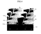
- FIG. 4 is a scanning electron microscope (SEM) picture illustrating a transmission area included in the embodiment of an organic light emitting diode display of FIG. 1 ;
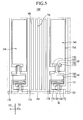
- FIG. 5 is a layout view illustrating a structure of a pixel of another embodiment of an organic light emitting diode display
- FIG. 6 is an SEM picture illustrating a transmission area included in the embodiment of an organic light emitting diode display of FIG. 5 ;
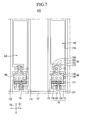
- FIG. 7 is a layout view illustrating a structure of a pixel of another embodiment of an organic light emitting diode display
- FIG. 8 is a layout view illustrating a structure of a pixel of another embodiment of an organic light emitting diode display
- FIG. 9 is a cross-sectional view of an embodiment of a touch controlled display device.
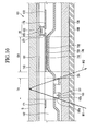
- FIG. 10 is a cross-sectional view of main parts in the embodiment of a touch controlled display device of FIG. 9 ;
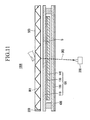
- FIG. 11 is a cross-sectional view of another embodiment of a touch controlled display device.
- FIG. 12 is a cross-sectional view of another embodiment of a touch controlled display device.
- FIGS. 1 through 4 an embodiment of an organic light emitting diode display will be described.
- FIG. 1 is a cross-sectional view of an embodiment of an organic light emitting diode display.
- the organic light emitting diode display 101 includes a first substrate 110, a second substrate 120, a wiring part 130, and an organic light emitting element 140.
- the first substrate 110 and the second substrate 120 may be an optically transmissive and electrically insulating substrate, containing glass, a polymer, or the like.
- the first substrate 110 and the second substrate 120 face each other and are attached to one another by a sealant.
- the wiring part 130 and the organic light emitting element 140 are positioned between the first substrate 110 and the second substrate 120.
- the first substrate 110 and the second substrate 120 may protect the wiring part 130 and the organic light emitting element 140 from external interference.
- the wiring part 130 includes switching and driving thin film transistors 10 and 20 (shown in FIG. 2 ) and may transmit a driving signal to the organic light emitting element 140 to drive the organic light emitting element 140.
- the organic light emitting element 140 may emit light depending on the signal transmitted from the wiring part 130.
- the organic light emitting element 140 is positioned on the wiring part 130.
- the organic light emitting element 140 is positioned at a display region on the first substrate 110 and may be formed by a vacuum deposition method using a mask, by a printing method, or the like.
- the organic light emitting element 140 may receive the signal from the wiring part 130 and may display an image by the received signal.
- the organic light emitting diode display 101 includes a transmission area TA (shown in FIG. 2 ) where light irradiated from the outside is transmitted, and a display area DA (shown in FIG. 2 ) displaying the image.
- FIG. 2 is a layout view illustrating a structure of a pixel of the embodiment of an organic light emitting diode display of FIG. 1 .
- FIG. 3 is a cross-sectional view taken along line III-III of FIG. 2 .
- the wiring part 130 and the organic light emitting element 140 may be formed in various different structures which can be easily modified by those skilled in the art.
- the organic light emitting diode display may be an active matrix (AM) type organic light emitting diode display having a 2Tr-lCap structure, which is provided with two thin film transistors (TFTs) and one storage capacitor in one pixel as shown.
- TFTs thin film transistors
- the number of thin film transistors, the number of storage capacitors, and the number of wires may vary.
- a pixel represents the minimum unit displaying an image and the organic light emitting diode display generally displays the image through a plurality of pixels.
- the organic light emitting diode display 101 includes a switching thin film transistor 10, a driving thin film transistor 20, a storage capacitor 80, and an organic light emitting element 140 for each pixel.
- the wiring part 130 includes the switching thin film transistor 10, the driving thin film transistor 20, and the storage capacitor 80 .
- the wiring part 130 also includes a gate line 151 disposed in a first direction D1 of the first substrate 110, and a data line 171 and a common power supply line 172 insulatively crossing the gate line 151 in a second direction D2 crossing the first direction D1.
- a boundary of one pixel may be defined by the gate line 151, the data line 171, and the common power line 172.
- the switching thin film transistor 10 includes a switching semiconductor layer 131, a switching gate electrode 152, a switching source electrode 173, and a switching drain electrode 174.
- the driving thin film transistor 20 includes a driving semiconductor layer 132, a driving gate electrode 155, a driving source electrode 176, and a driving drain electrode 177.
- the switching thin film transistor 10 serves as a switch that selects a pixel to emit light.
- the switching gate electrode 152 is connected to the gate line 151.
- the switching source electrode 173 is connected to the data line 171.
- the switching drain electrode 174 is separate from the switching source electrode 173 and is connected to any one storage plate 158.
- the driving thin film transistor 20 applies driving voltage to allow an organic light emitting layer 720 of the organic light emitting element 140 in the selected pixel to emit light to a first pixel electrode 710.
- the driving gate electrode 155 is connected to the storage plate 158 connected with the switching drain electrode 174.
- Each of the driving source electrode 176 and the other storage plate 178 is connected to the common power supply line 172.
- a first electrode 710 of the organic light emitting element 140 extends from the driving drain electrode 177 and the driving drain electrode 177 and the first electrode 710 are interconnected.
- the storage capacitor 80 includes the pair of storage plates 158 and 178 with an interlayer insulating layer 161 interposed therebetween.
- the interlayer insulating layer 161 is made of a dielectric material, and a capacitance of the storage capacitor 80 is determined by an electric charge stored in the storage capacitor 80 and voltage between storage plates 158 and 178.
- the switching thin film transistor 10 is driven by gate voltage applied to the gate line 151, and transmits data voltage, applied to the data line 171, to the driving thin film transistor 20.
- a voltage corresponding to a difference between common voltage applied to the driving thin film transistor 20 from the common power supply line 172, and the data voltage transmitted from the switching thin film transistor 10, is stored in the storage capacitor 80.
- Current corresponding to the voltage stored in the storage capacitor 80 flows to the organic light emitting element 140 through the driving thin film transistor 20 to allow the organic light emitting element 140 to emit light.
- the organic light emitting element 140 includes a first electrode 710, an organic light emitting layer 720 formed on the first electrode 710, and a second electrode 730 formed on the organic light emitting layer 720.
- the organic light emitting layer 720 emitting light is positioned between the first electrode 710 and the second electrode 730 facing each other.
- the first electrode 710 may be an anode, serving as a hole injection electrode
- the second electrode 730 may be a cathode, serving as an electron injection electrode.
- the first electrode 710 may be the cathode
- the second electrode 730 may be the anode according to a driving method of the organic light emitting diode display 101. Holes and electrons may be injected into the organic light emitting layer 720 from the first electrode 710 and the second electrode 730, respectively. When an exciton generated by a combination of the holes and the electrons injected into the organic light emitting layer 720 falls from an excited state to a ground state, the organic light emitting layer 720 emits light.
- the first electrode 710 may include a single-layered or multilayered light transmitting conductive material including at least one of indium tin oxide (ITO), indium zinc oxide (IZO), and the like.
- the second electrode 730 may include a single-layered or multilayered light reflecting conductive material including at least one of aluminum (Al), silver (Ag) and the like.
- the first electrode 710 may be light-transmissive and the second electrode 730 may be light-reflective.
- the organic light emitting layer 720 may further include at least one of an electron injection layer, an electron transport layer, a hole injection layer, and a hole transport layer.
- the organic light emitting element 140 emits light in the direction of the first substrate 110.
- the organic light emitting diode display 101 is therefore a backlight type displaying an image by emitting light in an upper direction of the organic light emitting diode display 101.
- the organic light emitting diode display 101 further includes the transmission area TA and the display area DA.
- the display area DA includes the first electrode 710, the organic light emitting layer 720, and the second electrode 730.
- the display area DA displays an image by using light emitted from the organic light emitting layer 720.
- the transmission area TA is positioned adjacent the display area DA.
- a pixel defined layer 162 is positioned on the interlayer insulating layer 161 to expose the first electrode 710.
- the organic light emitting layer 720 and the second electrode 730 are positioned on the exposed first electrode 710.
- the pixel defined layer 162 may thus define the display area DA.
- the pixel defined layer 162 may be formed by a light transmitting organic layer containing polyimide, polyacryl, or the like.
- the pixel defined layer 162 may be formed by a light transmitting inorganic layer containing silicon nitride (SiNx), silicon oxide (Si02) or the like.
- the transmission area TA transmits light irradiated from the outside and includes a protruding portion 165 and a portion 731 of the second electrode 730.
- FIG. 4 is a scanning electron microscope (SEM) picture illustrating a transmission area included in this embodiment of an organic light emitting diode display of FIG. 1 .
- a plurality of protruding portions 165 are positioned between the first electrode 710 and the data line 171, and are positioned at a portion of the pixel defined by the gate line 151, the data line 171, and the common power supply line 172.
- Each protruding portion 165 protrudes from the pixel defined layer 162 and includes the same material used to form the pixel defined layer 162.
- the protruding portions 165 are spaced from each other and each has an island configuration.
- the side 165a of each protruding portion 165 is inversely tapered.
- the second electrode 730 is formed throughout the organic light emitting element 140 by using a deposition process.
- the sides 165a of the protruding portions 165 are inversely tapered, such that a portion 731 of the second electrode 730 is deposited on the top 165b of each protruding portion 165, but the second electrode 730 is not deposited on the sides 165a of the protruding portions 165.
- the portions 731 of the second electrode 730 that are seated on the top 165b of the protruding portions 165 are spaced from the entire second electrode 730 by spacing areas SA. Light irradiated from the outside can be transmitted through the spacing area SA.
- the transmission area TA is formed by the spacing areas SA formed by the protruding portions 165 and the light irradiated from the outside is transmitted through the transmission area TA.
- the portion 731 of the second electrode 730 that is deposited on the top 165b of each protruding portion 165 is dependent on at least the width and the height of the protruding portion 165 itself, the size of the gap between neighboring protruding portions 165, and the inclination level of the side 165a of the protruding portion 165.
- the dimension of the spacing area SA formed between a portion 731 of the second electrode 730 and the entire second electrode 730 may be selected to suit preferred operational characteristics of the device. For example, the dimension of the spacing areas SA may be increased to increase the transmission of the light irradiated from the outside.
- the protruding portion 165 may be formed using a MEMS process such as photolithography, and the like.
- the side 165b is inversely tapered using an etch ratio.
- the protruding portions 165 of the organic light emitting diode display 101 are positioned between the first electrode 710 and the data line 171. In other embodiments, the protruding portions of the organic light emitting diode display may be positioned between the first electrode 710 and the common power supply line 172.
- one layer protrudes from the pixel defined layer 162 to form the protruding portion 165 of the organic light emitting diode display 1 O l_ .
- a plurality of layers may protrude from the pixel defined layer 162 to form a laminated protruding portion.
- the organic light emitting diode display 101 includes the transmission area TA where a portion 731 of the second electrode 730 is spaced from the entire second electrode 730 by the spacing area SA by the protruding portion 165, such that the light irradiated from the outside is transmitted through the spacing area SA. Since the light irradiated from the outside penetrates the organic light emitting diode display 101 through the transmission area TA, the organic light emitting diode display 101 is implemented as a fully transparent organic light emitting diode display 101.
- FIG. 5 is a layout view illustrating a structure of a pixel of another embodiment of an organic light emitting diode display.
- FIG. 6 is an SEM picture illustrating a transmission area included in the embodiment of an organic light emitting diode display of FIG. 5 .
- the transmission area TA transmits light irradiated from the outside and includes a protruding portion 165 and a portion 731 of the second electrode 730.
- the protruding portion 165 is positioned between a data line 171 of any one pixel among adjacent pixels and a common power supply line 172 of the other pixel and in addition, it is positioned between the adjacent pixels.
- the side 165a of the protruding portion 165 is inversely tapered.
- the second electrode 730 is formed throughout the organic light emitting element 140 by using a deposition process.
- the side 165a of the protruding portion 165 is inversely tapered, such that a portion 731 of the second electrode 730 is deposited on the top 165b of the protruding portion 165, but the second electrode 730 is not deposited on the side 165a of the protruding portion 165. A portion 731 of the second electrode 730 is seated on the top 165b of the protruding portion 165.
- each second electrode 730 is seated on the top 165b of the protruding portion 165 having the inversely tapered side 165a so as to be spaced from the entire electrode 730 by a spacing area SA.
- Portions 731 of the second electrodes 730 are spaced from the entire second electrode 730 by the spacing areas SA, such that the light irradiated from the outside can be transmitted through the spacing areas SA.
- the transmission area TA is formed by the spacing areas SA formed by the protruding portions 165 and the light irradiated from the outside is transmitted through the transmission area TA.
- the protruding portion 165 of the organic light emitting diode display 102 in the embodiment of FIGS. 5 and 6 extends in the second direction D2 parallel to the extension direction of the data line 171 and the common power supply line 172.
- a protruding portion of an organic light emitting diode display may extend in a first direction D1 parallel to an extension direction of a gate line 151.
- the organic light emitting diode display 102 includes the transmission area TA where portions 731 of the second electrode 730 are spaced from the entire second electrode 730 by the spacing areas SA by the protruding portion 165, such that the light irradiated from the outside is transmitted through the spacing area SA. Since the light irradiated from the outside penetrates the organic light emitting diode display 102 through the transmission area TA, the organic light emitting diode display 102 is implemented as a fully transparent organic light emitting diode display 102.
- FIG. 7 is a layout view illustrating a structure of a pixel of another embodiment of an organic light emitting diode display.
- the transmission area TA transmits light irradiated from the outside and includes a protruding portion 165 and a portion 731 of the second electrode 730.
- the protruding portion 165 is positioned to correspond to a switching thin film transistor 10 and a driving thin film transistor 20 in a pixel defined by a gate line 151, a common power supply line 172, and a data line 171.
- a portion 731 of the second electrode 730 is spaced from the entire second electrode 730 by a spacing area SA on the top 165b of the protruding portion 165. Light irradiated from the outside is transmitted through the spacing area SA.
- the transmission area TA is formed by the spacing area SA formed by the protruding portion 165 and the light irradiated from the outside is transmitted through the transmission area TA.
- the switching thin film transistor 10 and the driving thin film transistor 20 are positioned to correspond to the transmission area TA, the light transmitted through the spacing area SA from the outside may penetrate the organic light emitting diode display 103 through a space between wires constituting the switching thin film transistor 10 and a space between wires constituting the driving thin film transistor 20.
- the organic light emitting diode display 103 includes the transmission area TA where a portion 731 of the second electrode 730 is spaced from the entire second electrode 730 by the spacing area SA by the protruding portion 165, such that the light irradiated from the outside is transmitted through the spacing area SA. Since the light irradiated from the outside penetrates the organic light emitting diode display 103 through the transmission area TA, the organic light emitting diode display 103 is implemented as a fully transparent organic light emitting diode display 103.
- FIG. 8 is a layout view illustrating a structure of a pixel of another embodiment of an organic light emitting diode display.
- the transmission area TA transmits light irradiated from the outside and includes a protruding portion 165 and a portion 731 of the second electrode 730.
- the protruding portion 165 is surrounded by a first electrode 710, a common power supply line 172, and a data line 171 in a pixel defined by a gate line 151, the common power supply line 172, and the data line 171. That is, the protruding portion 165 is adjacent to the first electrode 710, the common power supply line 172, and the data line 171.
- the protruding portion 165 is positioned adjacent to the first electrode 710, the common power supply line 172, and the data line 171.
- a portion 731 of the second electrode 730 is spaced from the entire second electrode 730 by a spacing area SA on the top 165b of the protruding portion 165.
- Light irradiated from the outside is transmitted through the spacing area SA.
- the transmission area TA is formed by the spacing area SA formed by the protruding portion 165 and the light irradiated from the outside is transmitted through the transmission area TA.
- the organic light emitting diode display 104 includes the transmission area TA where a portion 731 of the second electrode 730 is spaced from the entire second electrode 730 by the spacing area SA by the protruding portion 165, such that the light irradiated from the outside is transmitted through the spacing area SA. Since the light irradiated from the outside penetrates the organic light emitting diode display 104 through the transmission area TA, the organic light emitting diode display 104 is implemented as a fully transparent organic light emitting diode display 104.
- a touch controlled display device 1005 will be described.
- the embodiment of a touch controlled display device described includes the embodiment of the organic light emitting diode display 101 shown in FIG. 1
- the touch controlled display device may include other embodiments of the organic light emitting diode displays.
- FIG. 9 is a cross-sectional view of an embodiment of a touch controlled display device.
- the touch controlled display device 1005 recognizes a touch by using infrared rays and includes the embodiment of an organic light emitting diode display 101 shown in FIG. 1 , an infrared-ray source 200, an infrared-ray sensor 300, and an infrared-ray transmission layer 400.
- the organic light emitting diode display 101 includes a first substrate 110, a second substrate 120, a wiring part 130, and an organic light emitting element 140.
- FIG. 10 is a cross-sectional view of main parts in the embodiment of a touch controlled display device of FIG. 9 .
- an embodiment of the organic light emitting diode display 101 includes a display area DA displaying an image and a transmission area TA transmitting light irradiated from the outside.
- the transmission area TA of the organic light emitting diode display 101 transmits the light irradiated from the outside, and also transmits infrared rays.
- a first infrared ray IR1 irradiated from the infrared-ray source 200 is irradiated to the surface S of the first substrate 110 of the organic light emitting diode display 101 through a spacing area SA of the transmission area TA.
- the infrared-ray source 200 is positioned below the organic light emitting diode display 101 and irradiates the first infrared ray IR1 in the direction of the organic light emitting diode display 101.
- the first infrared ray IRI irradiated in the direction of the organic light emitting diode display 101 from the infrared-ray source 200 is irradiated to the surface S of the first substrate 110 included in the organic light emitting diode display 101 through the spacing area SA of the transmission area TA of the organic light emitting diode display 101.
- the first infrared ray IR1 irradiated to the organic light emitting diode display 101 from the infrared-ray source 200 corresponds to the surface S of the organic light emitting diode display 101.
- the amount of light of the first infrared ray IR1 is changed by a touch when the touch is performed on the surface S of the first substrate 110.
- the first infrared ray IR1 irradiated to the surface of the first substrate 110 from the infrared-ray source 200 is changed to a second infrared ray IR2 again reflected in the direction of the organic light emitting diode display 101.
- the second infrared ray IR2 is reflected from the surface S of the first substrate 110 and is irradiated to a lower direction of the organic light emitting diode display 101 through the spacing area SA of the transmission area TA of the organic light emitting diode display 101.
- the infrared-ray sensor 300 is positioned below the organic light emitting diode display 101 and senses the second infrared ray IR2.
- the infrared-ray sensor 300 may determine a touch point with respect to the organic light emitting diode display 101 by sensing the second infrared ray IR2.
- a touch signal for the touch point determined by the infrared-ray sensor 300 may be transmitted to a controller driving the organic light emitting diode display 101 to thereby display an image depending on the touch signal on the organic light emitting diode display 101.
- the infrared-ray sensor 300 senses the surface S of the first substrate 110 by sensing the infrared rays irradiated to the infrared-ray sensor 300 even though the touch is not performed on the surface S of the first substrate 110 and determines the touch point with respect to the organic light emitting diode display 101 by sensing the second infrared ray IR2 having an amount of light changed by the touch among the infrared rays irradiated to the infrared-ray sensor 300.
- the infrared-ray sensor 300 may be a camera sensing the infrared rays. In other embodiments, the infrared-ray sensor 300 may include a sensor sensing the infrared rays.
- An infrared-ray transmission layer 400 is positioned between the organic light emitting diode display 101 and the infrared-ray sensor 300.
- the infrared-ray transmission layer 400 transmits the first infrared ray IR1 and the second infrared ray IR2.
- the infrared-ray transmission layer 400 blocks a wavelength of a visible light region among light emitted from the organic light emitting element 140 of the organic light emitting diode display 101. The light emitted from the organic light emitting element 140 is blocked by the infrared-ray transmission layer 400 to thereby minimize interference in the first infrared ray IR1 or the second infrared ray IR2 by the light emitted from the organic light emitting element 140.
- the infrared-ray transmission layer 400 blocks the wavelength of the visible light region among the light emitted from the organic light emitting element 140, such that an inner part of the organic light emitting diode display 101 is prevented from being seen from the outside due to reflection of the light emitted from the organic light emitting element 140 by a constituent member positioned in the organic light emitting diode display 101. An overall display quality of the touch controlled display device 1005 is thus prevented from being deteriorated.
- the infrared-ray transmission layer 400 blocks the light of the visible light region of external light irradiated to the infrared-ray transmission layer 400 through the spacing area SA of the transmission area TA and the light emitted from the organic light emitting element 140 to prevent an inner part of the touch controlled display device 1005 from being seen from the outside through the organic light emitting diode display 101.
- the organic light emitting diode display 101 displaying the image includes the organic light emitting element 140 which is the self light emitting element, such that the touch controlled display device 1005 has an improved display quality than touch controlled display devices including a screen display displaying the image on a screen by using an liquid crystal display panel or a projector requiring an additional light emitting unit such as a backlight unit.
- the organic light emitting display 101 included in the touch controlled display device 1005 can have a thinner thickness than the screen display included in touch controlled display devices including the projector and the screen, the entire touch controlled display device 1005 can be implemented to be slimmer.
- the touch controlled display device 1005 since the first infrared ray IR1 irradiated in the direction of the surface S of the organic light emitting diode display 101 from the infrared-ray source 200 and the second infrared ray IR2 reflected from the surface S of the organic light emitting diode display 101 by a touch can easily penetrate the organic light emitting diode display 101 through the spacing area SA of the transmission area TA, the overall infrared-ray transmittance to the organic light emitting diode display 101 is improved.
- the overall infrared-rays transmittance to the organic light emitting diode display 101 is improved by the spacing area SA formed in the transmission area TA to thereby improve the recognition rate of the touch to the touch controlled display device 1005.
- the touch controlled display device 1005 substantially includes the transmission area TA transmitting light of all wavelengths, light of a visible light region wavelength is blocked by the infrared-ray transmission layer 400. Therefore, an inner part of the touch controlled display device 1005 is suppressed from being seen to the outside and as a result, the display quality of the touch controlled display device 1005 is improved.
- Embodiments of the touch controlled display device 1005 have improved display quality, are slim, and have improved touch recognition rate by improving the infrared-rays transmittance while using the infrared rays as a touch recognition means.
- FIG. 11 is a cross-sectional view of another embodiment of a touch controlled display device.
- the touch controlled display device 1006 includes an organic light emitting diode display 101, an infrared-ray source 200, an infrared-ray sensor 300, an infrared-ray transmission layer 400, and a total reflection plate 500.
- the infrared-ray source 200 is positioned on the organic light emitting diode display 101.
- the infrared-ray source 200 is positioned on the end of the total reflection plate 500 and irradiates a first infrared ray IR1 to the inside of the total reflection plate 500.
- the first infrared ray IR1 irradiated to the inside of the total reflection plate 500 is total-reflected in a direction parallel to a plate surface of the total reflection plate 500 in the total reflection plate 500 to correspond to the surface S of a first substrate 100 included in the organic light emitting diode display 101.
- the first infrared ray IR1 irradiated to the inside of the total reflection plate 500 corresponds to the surface S of the organic light emitting diode display 101.
- the total reflection plate 500 is positioned on the organic light emitting diode display 101 while being adjacent to the infrared-ray source 200 and total-reflects the first infrared ray IR1 irradiated from the infrared-ray source 200 therein.
- a touch is made on the surface of the total reflection plate 500, total reflection of the first infrared ray IR1 total-reflected in the total reflection plate 500 is broken by the touch, and the first infrared ray IR1 is changed to a second infrared ray IR2 irradiated in the direction of the organic light emitting diode display 101.
- the second infrared ray IR2 is changed from the first infrared ray IR1 total-reflected, is irradiated to a lower side of the organic light emitting diode display 101 through a spacing area SA of a transmission area TA of the organic light emitting diode display 101, and is sensed by the infrared-ray sensor 300.
- FIG. 12 is a cross-sectional view of another embodiment of a touch controlled display device.
- the touch controlled display device 1007 includes an organic light emitting diode display 101, an infrared-ray source 200, an infrared-ray sensor 300, an infrared-ray transmission layer 400, a total reflection plate 500, and a sensing plate 600.
- the infrared-ray source 200 is positioned on the organic light emitting diode display 101.
- the infrared-ray source 200 is positioned on the end of the total reflection plate 500 and irradiates a first infrared ray IR1 to the inside of the total reflection plate 500.
- the first infrared ray IR1 irradiated is total-reflected in a direction parallel to a plate surface of the total reflection plate 500 in the total reflection plate 500 to correspond to the surface S of a first substrate 110 included in the organic light emitting diode display 101.
- the first infrared ray IR1 irradiated to the inside of the total reflection plate 500 from the infrared-ray source 200 and total-reflected in the total reflection plate 500 corresponds to the surface S of the organic light emitting diode display 101.
- the total reflection plate 500 is positioned on the organic light emitting diode display 101 while being adjacent to the infrared-ray source 200 and total-reflects the first infrared ray IR1 irradiated from the infrared-ray source 200 therein.
- a touch is made on the surface of the total reflection plate 500, total reflection of the first infrared ray IR1 total-reflected in the total reflection plate 500 is broken by the touch and the first infrared ray IR1 is changed to a second infrared ray IR2 irradiated in the direction of the organic light emitting diode display 101.
- the second infrared ray IR2 is changed from the first infrared ray IR1 total-reflected, is irradiated to a lower side of the organic light emitting diode display 101 through a transmission area TA of the organic light emitting diode display 101, and is sensed by the infrared-rays sensor 300.
- infrared-ray sensors 300 there may be a plurality of infrared-ray sensors 300 these may be mounted on a sensing plate 600.
- the sensing plate 600 is positioned below the organic light emitting diode display 101 and is mounted with the plurality of infrared-rays sensors 300.
- the plurality of infrared-rays sensors 300 mounted on the sensing plate 600 may be all formed on the sensing plate 600 by using a MEMS process such as photolithography, and the like.
Landscapes
- Engineering & Computer Science (AREA)
- General Engineering & Computer Science (AREA)
- Theoretical Computer Science (AREA)
- Physics & Mathematics (AREA)
- Human Computer Interaction (AREA)
- General Physics & Mathematics (AREA)
- Optics & Photonics (AREA)
- Microelectronics & Electronic Packaging (AREA)
- Multimedia (AREA)
- Electroluminescent Light Sources (AREA)
- Devices For Indicating Variable Information By Combining Individual Elements (AREA)
Abstract
Description
- The present invention relates generally to an organic light emitting diode display including a transmission area and a touch controlled display device having the same.
- Touch controlled display devices are devices capable of controlling a display device by using touch. Touch controlled display devices using infrared rays have recently become popular.
- Generally, touch controlled display devices using infrared rays include a display device displaying an image, an infrared-ray source irradiating infrared rays to a part where the image is displayed, and an infrared ray sensor sensing infrared rays reflected from the part where the image is displayed.
- A screen display device for displaying an image onto a screen by using a projector, and a liquid crystal display device including a liquid crystal panel displaying an image by using a liquid crystal, and a backlight unit irradiating light to the liquid crystal panel are generally used.
- Touch controlled display devices using infrared rays including a screen display device may have a problem in that a display quality of the image emitted from the projector and displayed on the screen may not be satisfactory due to the technical limits of the projector. The overall size of the touch controlled display devices may also be increased because a predetermined clearance space may be required between the projector and the screen.
- Also, in some infrared-ray touch controlled display devices including a liquid crystal display device, the infrared rays irradiated from the infrared-ray source may need to be transmitted to the liquid crystal panel and the infrared rays reflected from the liquid crystal panel may need to be transmitted to the liquid crystal panel. In such devices, transmittance of the infrared rays to the liquid crystal panel may be deteriorated by a shutter function of the liquid crystal included in the liquid crystal panel. If transmittance of the infrared rays to the liquid crystal panel is deteriorated, the recognition rate of a touch to the touch controlled display device may be deteriorated.
- The information disclosed in this Background section is merely for enhancement of understanding of the background of the described technology.
- The invention sets out to provide an organic light emitting diode display having an improved infrared-ray transmittance.
- The described technology has been made in an effort to provide a touch controlled display device having improved display quality, slim size, and improved touch recognition rate while using infrared rays as a touch recognition means, including the organic light emitting diode display having the improve infrared-rays transmittance.
- According to one aspect of the invention, an organic light emitting diode display, includes: a display area including an organic light emitting layer emitting light, and a first electrode and a second electrode facing each other, the organic light emitting layer interposed between the first and second electrodes, and a transmission area adjacent to the display area, including a portion of the second electrode spaced away from the second electrode by a spacing area and a protruding portion on which the portion of the second electrode is seated, configured to transmit light irradiated from the outside through the spacing area.
- Another aspect of the invention provides a touch controlled display device, including: an organic light emitting display including: a display area including an organic light emitting layer emitting light, a first electrode and a second electrode facing each other, with the organic light emitting layer interposed between the first and second electrodes, and a transmission area adjacent to the display area, including a portion of the second electrode spaced away from the second electrode by a spacing area and a protruding portion on which the portion of the second electrode is seated, configured to transmit light irradiated from the outside through the spacing area, an infrared-ray source configured to irradiate a first infrared ray along the surface of the organic light emitting diode, and an infrared-ray sensor positioned below the organic light emitting diode display and configured to sense a second infrared ray that is irradiated in the direction of the organic light emitting diode display from the first infrared ray by using a touch and transmitted throughout the transmission area .
- Another aspect of the invention provides a touch controlled display device, including: an organic light emitting display including a display area and a transmission area adjacent to the display area, an infrared-ray source positioned on the organic light emitting diode display, configured to irradiate a first infrared ray onto a surface of the organic light emitting diode display, a total reflection plate positioned on the organic light emitting diode display, adjacent to the infrared-ray source and configured to total-reflect the first infrared ray irradiated from the infrared-ray source therein, an infrared-ray sensor positioned below the organic light emitting diode display and configured to sense a second infrared ray irradiated in the direction of the organic light emitting diode display from the first infrared ray, by a touch of the total reflection plate, and transmitted throughout the transmission area.
[0012a] At least some of the above and other features of the invention are set out in the appended claims. -
FIG. 1 is a cross-sectional view of an embodiment of an organic light emitting diode display; -
FIG. 2 is a layout view illustrating a structure of a pixel of the embodiment of an organic light emitting diode display ofFIG. 1 ; -
FIG. 3 is a cross-sectional view taken along line III-III ofFIG. 2 ; -
FIG. 4 is a scanning electron microscope (SEM) picture illustrating a transmission area included in the embodiment of an organic light emitting diode display ofFIG. 1 ; -
FIG. 5 is a layout view illustrating a structure of a pixel of another embodiment of an organic light emitting diode display; -
FIG. 6 is an SEM picture illustrating a transmission area included in the embodiment of an organic light emitting diode display ofFIG. 5 ; -
FIG. 7 is a layout view illustrating a structure of a pixel of another embodiment of an organic light emitting diode display; -
FIG. 8 is a layout view illustrating a structure of a pixel of another embodiment of an organic light emitting diode display; -
FIG. 9 is a cross-sectional view of an embodiment of a touch controlled display device; -
FIG. 10 is a cross-sectional view of main parts in the embodiment of a touch controlled display device ofFIG. 9 ; -
FIG. 11 is a cross-sectional view of another embodiment of a touch controlled display device; and -
FIG. 12 is a cross-sectional view of another embodiment of a touch controlled display device. - Embodiments of the invention will be described more fully hereinafter with reference to the accompanying drawings, in which certain embodiments are shown. As those skilled in the art would realize, the described embodiments may be modified in various ways, without departing from the scope of the present invention.
- The drawings and description are to be regarded as illustrative in nature and not restrictive. Like reference numerals generally designate like elements throughout the specification.
- The size and thickness of each component shown in the drawings are arbitrarily shown for understanding and ease of description.
- In the drawings, the thickness of layers, films, panels, regions, and the like are exaggerated for clarity. It will be understood that when an element such as a layer, film, region, or substrate is referred to as being "on" or "below" another element, it can be "directly on" or "directly below" the other element, or intervening elements may also be present.
- Throughout the disclosure, unless explicitly described to the contrary, the word "comprise" and variations such as "comprises" or "comprising", will be understood to imply the inclusion of stated elements but not the exclusion of any other elements. Further, throughout the specification, "on" or "below" implies being positioned above or below a target element and does not imply being necessarily positioned on the top or on the basis of a gravity direction.
- Hereinafter, referring to
FIGS. 1 through 4 , an embodiment of an organic light emitting diode display will be described. -
FIG. 1 is a cross-sectional view of an embodiment of an organic light emitting diode display. - The organic light
emitting diode display 101 includes afirst substrate 110, asecond substrate 120, awiring part 130, and an organiclight emitting element 140. - The
first substrate 110 and thesecond substrate 120 may be an optically transmissive and electrically insulating substrate, containing glass, a polymer, or the like. Thefirst substrate 110 and thesecond substrate 120 face each other and are attached to one another by a sealant. Thewiring part 130 and the organiclight emitting element 140 are positioned between thefirst substrate 110 and thesecond substrate 120. Thefirst substrate 110 and thesecond substrate 120 may protect thewiring part 130 and the organiclight emitting element 140 from external interference. - The
wiring part 130 includes switching and drivingthin film transistors 10 and 20 (shown inFIG. 2 ) and may transmit a driving signal to the organiclight emitting element 140 to drive the organiclight emitting element 140. The organiclight emitting element 140 may emit light depending on the signal transmitted from thewiring part 130. - The organic
light emitting element 140 is positioned on thewiring part 130. - The organic
light emitting element 140 is positioned at a display region on thefirst substrate 110 and may be formed by a vacuum deposition method using a mask, by a printing method, or the like. The organiclight emitting element 140 may receive the signal from thewiring part 130 and may display an image by the received signal. - The organic light
emitting diode display 101 includes a transmission area TA (shown inFIG. 2 ) where light irradiated from the outside is transmitted, and a display area DA (shown inFIG. 2 ) displaying the image. -
FIG. 2 is a layout view illustrating a structure of a pixel of the embodiment of an organic light emitting diode display ofFIG. 1 .FIG. 3 is a cross-sectional view taken along line III-III ofFIG. 2 . - One embodiment of the detailed structures of the
wiring part 130 and the organiclight emitting element 140 is shown inFIGS. 2 and3 . In other embodiments, thewiring part 130 and the organiclight emitting element 140 may be formed in various different structures which can be easily modified by those skilled in the art. In some embodiments, the organic light emitting diode display may be an active matrix (AM) type organic light emitting diode display having a 2Tr-lCap structure, which is provided with two thin film transistors (TFTs) and one storage capacitor in one pixel as shown. In other embodiments, the number of thin film transistors, the number of storage capacitors, and the number of wires may vary. A pixel represents the minimum unit displaying an image and the organic light emitting diode display generally displays the image through a plurality of pixels. - As shown in
FIGS. 2 and3 , the organic lightemitting diode display 101 includes a switchingthin film transistor 10, a drivingthin film transistor 20, astorage capacitor 80, and an organiclight emitting element 140 for each pixel. - In this embodiment, the
wiring part 130 includes the switchingthin film transistor 10, the drivingthin film transistor 20, and thestorage capacitor 80 . Thewiring part 130 also includes agate line 151 disposed in a first direction D1 of thefirst substrate 110, and adata line 171 and a commonpower supply line 172 insulatively crossing thegate line 151 in a second direction D2 crossing the first direction D1. In this embodiment, a boundary of one pixel may be defined by thegate line 151, thedata line 171, and thecommon power line 172. - The switching
thin film transistor 10 includes a switchingsemiconductor layer 131, a switching gate electrode 152, a switching source electrode 173, and aswitching drain electrode 174. The drivingthin film transistor 20 includes a drivingsemiconductor layer 132, a drivinggate electrode 155, a drivingsource electrode 176, and a drivingdrain electrode 177. - The switching
thin film transistor 10 serves as a switch that selects a pixel to emit light. The switching gate electrode 152 is connected to thegate line 151. The switching source electrode 173 is connected to thedata line 171. The switchingdrain electrode 174 is separate from the switching source electrode 173 and is connected to any onestorage plate 158. - The driving
thin film transistor 20 applies driving voltage to allow an organiclight emitting layer 720 of the organiclight emitting element 140 in the selected pixel to emit light to afirst pixel electrode 710. The drivinggate electrode 155 is connected to thestorage plate 158 connected with the switchingdrain electrode 174. Each of the drivingsource electrode 176 and theother storage plate 178 is connected to the commonpower supply line 172. Afirst electrode 710 of the organiclight emitting element 140 extends from the drivingdrain electrode 177 and the drivingdrain electrode 177 and thefirst electrode 710 are interconnected. - The
storage capacitor 80 includes the pair ofstorage plates layer 161 interposed therebetween. In this embodiment, theinterlayer insulating layer 161 is made of a dielectric material, and a capacitance of thestorage capacitor 80 is determined by an electric charge stored in thestorage capacitor 80 and voltage betweenstorage plates - The switching
thin film transistor 10 is driven by gate voltage applied to thegate line 151, and transmits data voltage, applied to thedata line 171, to the drivingthin film transistor 20. A voltage corresponding to a difference between common voltage applied to the drivingthin film transistor 20 from the commonpower supply line 172, and the data voltage transmitted from the switchingthin film transistor 10, is stored in thestorage capacitor 80. Current corresponding to the voltage stored in thestorage capacitor 80 flows to the organiclight emitting element 140 through the drivingthin film transistor 20 to allow the organiclight emitting element 140 to emit light. - The organic
light emitting element 140 includes afirst electrode 710, an organiclight emitting layer 720 formed on thefirst electrode 710, and asecond electrode 730 formed on the organiclight emitting layer 720. The organiclight emitting layer 720 emitting light is positioned between thefirst electrode 710 and thesecond electrode 730 facing each other. - In one embodiment, the
first electrode 710 may be an anode, serving as a hole injection electrode, and thesecond electrode 730 may be a cathode, serving as an electron injection electrode. In other embodiments, thefirst electrode 710 may be the cathode and thesecond electrode 730 may be the anode according to a driving method of the organic light emittingdiode display 101. Holes and electrons may be injected into the organiclight emitting layer 720 from thefirst electrode 710 and thesecond electrode 730, respectively. When an exciton generated by a combination of the holes and the electrons injected into the organiclight emitting layer 720 falls from an excited state to a ground state, the organiclight emitting layer 720 emits light. In some embodiments, thefirst electrode 710 may include a single-layered or multilayered light transmitting conductive material including at least one of indium tin oxide (ITO), indium zinc oxide (IZO), and the like. In some embodiments, thesecond electrode 730 may include a single-layered or multilayered light reflecting conductive material including at least one of aluminum (Al), silver (Ag) and the like. In such embodiments, thefirst electrode 710 may be light-transmissive and thesecond electrode 730 may be light-reflective. In some embodiments, the organiclight emitting layer 720 may further include at least one of an electron injection layer, an electron transport layer, a hole injection layer, and a hole transport layer. - In this embodiment of the organic light emitting
diode display 101, the organiclight emitting element 140 emits light in the direction of thefirst substrate 110. The organic light emittingdiode display 101 is therefore a backlight type displaying an image by emitting light in an upper direction of the organic light emittingdiode display 101. - The organic light emitting
diode display 101 further includes the transmission area TA and the display area DA. - The display area DA includes the
first electrode 710, the organiclight emitting layer 720, and thesecond electrode 730. The display area DA displays an image by using light emitted from the organiclight emitting layer 720. The transmission area TA is positioned adjacent the display area DA. - A pixel defined
layer 162 is positioned on theinterlayer insulating layer 161 to expose thefirst electrode 710. The organiclight emitting layer 720 and thesecond electrode 730 are positioned on the exposedfirst electrode 710. The pixel definedlayer 162 may thus define the display area DA. In some embodiments, the pixel definedlayer 162 may be formed by a light transmitting organic layer containing polyimide, polyacryl, or the like. In other embodiments, the pixel definedlayer 162 may be formed by a light transmitting inorganic layer containing silicon nitride (SiNx), silicon oxide (Si02) or the like. - The transmission area TA transmits light irradiated from the outside and includes a protruding
portion 165 and aportion 731 of thesecond electrode 730. -
FIG. 4 is a scanning electron microscope (SEM) picture illustrating a transmission area included in this embodiment of an organic light emitting diode display ofFIG. 1 . - As shown in
FIGS. 2 to 4 , a plurality of protrudingportions 165 are positioned between thefirst electrode 710 and thedata line 171, and are positioned at a portion of the pixel defined by thegate line 151, thedata line 171, and the commonpower supply line 172. Each protrudingportion 165 protrudes from the pixel definedlayer 162 and includes the same material used to form the pixel definedlayer 162. The protrudingportions 165 are spaced from each other and each has an island configuration. Theside 165a of each protrudingportion 165 is inversely tapered. Thesecond electrode 730 is formed throughout the organiclight emitting element 140 by using a deposition process. Thesides 165a of the protrudingportions 165 are inversely tapered, such that aportion 731 of thesecond electrode 730 is deposited on the top 165b of each protrudingportion 165, but thesecond electrode 730 is not deposited on thesides 165a of the protrudingportions 165. - The
portions 731 of thesecond electrode 730 that are seated on the top 165b of the protrudingportions 165 are spaced from the entiresecond electrode 730 by spacing areas SA. Light irradiated from the outside can be transmitted through the spacing area SA. The transmission area TA is formed by the spacing areas SA formed by the protrudingportions 165 and the light irradiated from the outside is transmitted through the transmission area TA. - The
portion 731 of thesecond electrode 730 that is deposited on the top 165b of each protrudingportion 165 is dependent on at least the width and the height of the protrudingportion 165 itself, the size of the gap between neighboring protrudingportions 165, and the inclination level of theside 165a of the protrudingportion 165. The dimension of the spacing area SA formed between aportion 731 of thesecond electrode 730 and the entiresecond electrode 730 may be selected to suit preferred operational characteristics of the device. For example, the dimension of the spacing areas SA may be increased to increase the transmission of the light irradiated from the outside. As the height of the protrudingportions 165 increases, the distance between theportion 731 of thesecond electrode 730 deposited on the top 165b of the protrudingportion 165 and thesecond electrode 730 increases, such that the dimension of the spacing area SA increases. The dimension of the spacing area SA is in proportion to the height of the protrudingportion 165 and as the height of the protrudingportion 165 increases, deposition interference of thesecond electrode 730 by the protrudingportion 165 occurs, such that the dimension of the spacing area SA increases to thereby improve external light transmittance through the transmission area TA. In some embodiments, the protrudingportion 165 may be formed using a MEMS process such as photolithography, and the like. In one embodiment, theside 165b is inversely tapered using an etch ratio. - In the embodiment of
FIG. 1 , the protrudingportions 165 of the organic light emittingdiode display 101 are positioned between thefirst electrode 710 and thedata line 171. In other embodiments, the protruding portions of the organic light emitting diode display may be positioned between thefirst electrode 710 and the commonpower supply line 172. - In this embodiment one layer protrudes from the pixel defined
layer 162 to form the protrudingportion 165 of the organic light emitting diode display 1 O l_ . In other embodiments, a plurality of layers may protrude from the pixel definedlayer 162 to form a laminated protruding portion. - One embodiment of the organic light emitting
diode display 101 includes the transmission area TA where aportion 731 of thesecond electrode 730 is spaced from the entiresecond electrode 730 by the spacing area SA by the protrudingportion 165, such that the light irradiated from the outside is transmitted through the spacing area SA. Since the light irradiated from the outside penetrates the organic light emittingdiode display 101 through the transmission area TA, the organic light emittingdiode display 101 is implemented as a fully transparent organic light emittingdiode display 101. - The light irradiated from the outside penetrates the organic light emitting
diode display 101 through the transmission area TA, such that when infrared rays are transmitted through the transmission area TA, infrared-ray transmittance of the organic light emittingdiode display 101 is improved. - Other embodiments of the organic light emitting diode display are described below. Only characteristic parts of the organic light emitting diode display according to the other embodiments different than the organic light emitting diode display according to the embodiment of
FIG. 1 will be described. -
FIG. 5 is a layout view illustrating a structure of a pixel of another embodiment of an organic light emitting diode display.FIG. 6 is an SEM picture illustrating a transmission area included in the embodiment of an organic light emitting diode display ofFIG. 5 . - As shown in
FIGS. 5 and6 , the transmission area TA transmits light irradiated from the outside and includes a protrudingportion 165 and aportion 731 of thesecond electrode 730. - In this embodiment, the protruding
portion 165 is positioned between adata line 171 of any one pixel among adjacent pixels and a commonpower supply line 172 of the other pixel and in addition, it is positioned between the adjacent pixels. There are a plurality of protrudingportions 165 and the plurality extends in a second direction D2 parallel to an extension direction of thedata line 171 and the commonpower supply line 172. Theside 165a of the protrudingportion 165 is inversely tapered. Thesecond electrode 730 is formed throughout the organiclight emitting element 140 by using a deposition process. Theside 165a of the protrudingportion 165 is inversely tapered, such that aportion 731 of thesecond electrode 730 is deposited on the top 165b of the protrudingportion 165, but thesecond electrode 730 is not deposited on theside 165a of the protrudingportion 165. Aportion 731 of thesecond electrode 730 is seated on the top 165b of the protrudingportion 165. - A
portion 731 of eachsecond electrode 730 is seated on the top 165b of the protrudingportion 165 having the inversely taperedside 165a so as to be spaced from theentire electrode 730 by a spacing area SA.Portions 731 of thesecond electrodes 730 are spaced from the entiresecond electrode 730 by the spacing areas SA, such that the light irradiated from the outside can be transmitted through the spacing areas SA. The transmission area TA is formed by the spacing areas SA formed by the protrudingportions 165 and the light irradiated from the outside is transmitted through the transmission area TA. - The protruding
portion 165 of the organic light emittingdiode display 102 in the embodiment ofFIGS. 5 and6 extends in the second direction D2 parallel to the extension direction of thedata line 171 and the commonpower supply line 172. In other embodiments, a protruding portion of an organic light emitting diode display may extend in a first direction D1 parallel to an extension direction of agate line 151. - In this embodiment, the organic light emitting
diode display 102 includes the transmission area TA whereportions 731 of thesecond electrode 730 are spaced from the entiresecond electrode 730 by the spacing areas SA by the protrudingportion 165, such that the light irradiated from the outside is transmitted through the spacing area SA. Since the light irradiated from the outside penetrates the organic light emittingdiode display 102 through the transmission area TA, the organic light emittingdiode display 102 is implemented as a fully transparent organic light emittingdiode display 102. -
FIG. 7 is a layout view illustrating a structure of a pixel of another embodiment of an organic light emitting diode display. - In the embodiment shown in
FIG. 7 , the transmission area TA transmits light irradiated from the outside and includes a protrudingportion 165 and aportion 731 of thesecond electrode 730. - The protruding
portion 165 is positioned to correspond to a switchingthin film transistor 10 and a drivingthin film transistor 20 in a pixel defined by agate line 151, a commonpower supply line 172, and adata line 171. Aportion 731 of thesecond electrode 730 is spaced from the entiresecond electrode 730 by a spacing area SA on the top 165b of the protrudingportion 165. Light irradiated from the outside is transmitted through the spacing area SA. The transmission area TA is formed by the spacing area SA formed by the protrudingportion 165 and the light irradiated from the outside is transmitted through the transmission area TA. - Although the switching
thin film transistor 10 and the drivingthin film transistor 20 are positioned to correspond to the transmission area TA, the light transmitted through the spacing area SA from the outside may penetrate the organic light emittingdiode display 103 through a space between wires constituting the switchingthin film transistor 10 and a space between wires constituting the drivingthin film transistor 20. - In the embodiment shown in
FIG. 7 , the organic light emittingdiode display 103 includes the transmission area TA where aportion 731 of thesecond electrode 730 is spaced from the entiresecond electrode 730 by the spacing area SA by the protrudingportion 165, such that the light irradiated from the outside is transmitted through the spacing area SA. Since the light irradiated from the outside penetrates the organic light emittingdiode display 103 through the transmission area TA, the organic light emittingdiode display 103 is implemented as a fully transparent organic light emittingdiode display 103. -
FIG. 8 is a layout view illustrating a structure of a pixel of another embodiment of an organic light emitting diode display. In the embodiment ofFIG. 8 , the transmission area TA transmits light irradiated from the outside and includes a protrudingportion 165 and aportion 731 of thesecond electrode 730. - The protruding
portion 165 is surrounded by afirst electrode 710, a commonpower supply line 172, and adata line 171 in a pixel defined by agate line 151, the commonpower supply line 172, and thedata line 171. That is, the protrudingportion 165 is adjacent to thefirst electrode 710, the commonpower supply line 172, and thedata line 171. - The protruding
portion 165 is positioned adjacent to thefirst electrode 710, the commonpower supply line 172, and thedata line 171. Aportion 731 of thesecond electrode 730 is spaced from the entiresecond electrode 730 by a spacing area SA on the top 165b of the protrudingportion 165. Light irradiated from the outside is transmitted through the spacing area SA. The transmission area TA is formed by the spacing area SA formed by the protrudingportion 165 and the light irradiated from the outside is transmitted through the transmission area TA. - In the embodiment shown in
FIG. 8 , the organic light emittingdiode display 104 includes the transmission area TA where aportion 731 of thesecond electrode 730 is spaced from the entiresecond electrode 730 by the spacing area SA by the protrudingportion 165, such that the light irradiated from the outside is transmitted through the spacing area SA. Since the light irradiated from the outside penetrates the organic light emittingdiode display 104 through the transmission area TA, the organic light emittingdiode display 104 is implemented as a fully transparent organic light emittingdiode display 104. - Referring to
FIGS. 9 to 10 , an embodiment of a touch controlleddisplay device 1005 will be described. The embodiment of a touch controlled display device described includes the embodiment of the organic light emittingdiode display 101 shown inFIG. 1 In other embodiments, the touch controlled display device may include other embodiments of the organic light emitting diode displays. -
FIG. 9 is a cross-sectional view of an embodiment of a touch controlled display device. - In the embodiment shown in
FIG. 9 , the touch controlleddisplay device 1005 recognizes a touch by using infrared rays and includes the embodiment of an organic light emittingdiode display 101 shown inFIG. 1 , an infrared-ray source 200, an infrared-ray sensor 300, and an infrared-ray transmission layer 400. - The organic light emitting
diode display 101 includes afirst substrate 110, asecond substrate 120, awiring part 130, and an organiclight emitting element 140. -
FIG. 10 is a cross-sectional view of main parts in the embodiment of a touch controlled display device ofFIG. 9 . - In the embodiment shown in
FIG. 10 , an embodiment of the organic light emittingdiode display 101 includes a display area DA displaying an image and a transmission area TA transmitting light irradiated from the outside. - The transmission area TA of the organic light emitting
diode display 101 transmits the light irradiated from the outside, and also transmits infrared rays. A first infrared ray IR1 irradiated from the infrared-ray source 200 is irradiated to the surface S of thefirst substrate 110 of the organic light emittingdiode display 101 through a spacing area SA of the transmission area TA. - Referring to
FIGS. 9 and10 , the infrared-ray source 200 is positioned below the organic light emittingdiode display 101 and irradiates the first infrared ray IR1 in the direction of the organic light emittingdiode display 101. The first infrared ray IRI irradiated in the direction of the organic light emittingdiode display 101 from the infrared-ray source 200 is irradiated to the surface S of thefirst substrate 110 included in the organic light emittingdiode display 101 through the spacing area SA of the transmission area TA of the organic light emittingdiode display 101. The first infrared ray IR1 irradiated to the organic light emittingdiode display 101 from the infrared-ray source 200 corresponds to the surface S of the organic light emittingdiode display 101. - The amount of light of the first infrared ray IR1 is changed by a touch when the touch is performed on the surface S of the
first substrate 110. The first infrared ray IR1 irradiated to the surface of thefirst substrate 110 from the infrared-ray source 200 is changed to a second infrared ray IR2 again reflected in the direction of the organic light emittingdiode display 101. The second infrared ray IR2 is reflected from the surface S of thefirst substrate 110 and is irradiated to a lower direction of the organic light emittingdiode display 101 through the spacing area SA of the transmission area TA of the organic light emittingdiode display 101. - The infrared-
ray sensor 300 is positioned below the organic light emittingdiode display 101 and senses the second infrared ray IR2. The infrared-ray sensor 300 may determine a touch point with respect to the organic light emittingdiode display 101 by sensing the second infrared ray IR2. A touch signal for the touch point determined by the infrared-ray sensor 300 may be transmitted to a controller driving the organic light emittingdiode display 101 to thereby display an image depending on the touch signal on the organic light emittingdiode display 101. The infrared-ray sensor 300 senses the surface S of thefirst substrate 110 by sensing the infrared rays irradiated to the infrared-ray sensor 300 even though the touch is not performed on the surface S of thefirst substrate 110 and determines the touch point with respect to the organic light emittingdiode display 101 by sensing the second infrared ray IR2 having an amount of light changed by the touch among the infrared rays irradiated to the infrared-ray sensor 300. In some embodiments, the infrared-ray sensor 300 may be a camera sensing the infrared rays. In other embodiments, the infrared-ray sensor 300 may include a sensor sensing the infrared rays. - An infrared-
ray transmission layer 400 is positioned between the organic light emittingdiode display 101 and the infrared-ray sensor 300. The infrared-ray transmission layer 400 transmits the first infrared ray IR1 and the second infrared ray IR2. The infrared-ray transmission layer 400 blocks a wavelength of a visible light region among light emitted from the organiclight emitting element 140 of the organic light emittingdiode display 101. The light emitted from the organiclight emitting element 140 is blocked by the infrared-ray transmission layer 400 to thereby minimize interference in the first infrared ray IR1 or the second infrared ray IR2 by the light emitted from the organiclight emitting element 140. - The infrared-
ray transmission layer 400 blocks the wavelength of the visible light region among the light emitted from the organiclight emitting element 140, such that an inner part of the organic light emittingdiode display 101 is prevented from being seen from the outside due to reflection of the light emitted from the organiclight emitting element 140 by a constituent member positioned in the organic light emittingdiode display 101. An overall display quality of the touch controlleddisplay device 1005 is thus prevented from being deteriorated. - The infrared-
ray transmission layer 400 blocks the light of the visible light region of external light irradiated to the infrared-ray transmission layer 400 through the spacing area SA of the transmission area TA and the light emitted from the organiclight emitting element 140 to prevent an inner part of the touch controlleddisplay device 1005 from being seen from the outside through the organic light emittingdiode display 101. - The organic light emitting
diode display 101 displaying the image includes the organiclight emitting element 140 which is the self light emitting element, such that the touch controlleddisplay device 1005 has an improved display quality than touch controlled display devices including a screen display displaying the image on a screen by using an liquid crystal display panel or a projector requiring an additional light emitting unit such as a backlight unit. - Since the organic
light emitting display 101 included in the touch controlleddisplay device 1005 can have a thinner thickness than the screen display included in touch controlled display devices including the projector and the screen, the entire touch controlleddisplay device 1005 can be implemented to be slimmer. - In the touch controlled
display device 1005, since the first infrared ray IR1 irradiated in the direction of the surface S of the organic light emittingdiode display 101 from the infrared-ray source 200 and the second infrared ray IR2 reflected from the surface S of the organic light emittingdiode display 101 by a touch can easily penetrate the organic light emittingdiode display 101 through the spacing area SA of the transmission area TA, the overall infrared-ray transmittance to the organic light emittingdiode display 101 is improved. The overall infrared-rays transmittance to the organic light emittingdiode display 101 is improved by the spacing area SA formed in the transmission area TA to thereby improve the recognition rate of the touch to the touch controlleddisplay device 1005. - Although the touch controlled
display device 1005 substantially includes the transmission area TA transmitting light of all wavelengths, light of a visible light region wavelength is blocked by the infrared-ray transmission layer 400. Therefore, an inner part of the touch controlleddisplay device 1005 is suppressed from being seen to the outside and as a result, the display quality of the touch controlleddisplay device 1005 is improved. - Embodiments of the touch controlled
display device 1005 have improved display quality, are slim, and have improved touch recognition rate by improving the infrared-rays transmittance while using the infrared rays as a touch recognition means. - Other embodiments of touch controlled display devices will be described below. Only characteristic parts of the touch controlled display devices different than the previously described embodiments will be described
-
FIG. 11 is a cross-sectional view of another embodiment of a touch controlled display device. - In the embodiment shown in
FIG. 11 , the touch controlleddisplay device 1006 includes an organic light emittingdiode display 101, an infrared-ray source 200, an infrared-ray sensor 300, an infrared-ray transmission layer 400, and atotal reflection plate 500. - The infrared-
ray source 200 is positioned on the organic light emittingdiode display 101. The infrared-ray source 200 is positioned on the end of thetotal reflection plate 500 and irradiates a first infrared ray IR1 to the inside of thetotal reflection plate 500. The first infrared ray IR1 irradiated to the inside of thetotal reflection plate 500 is total-reflected in a direction parallel to a plate surface of thetotal reflection plate 500 in thetotal reflection plate 500 to correspond to the surface S of a first substrate 100 included in the organic light emittingdiode display 101. The first infrared ray IR1 irradiated to the inside of thetotal reflection plate 500 corresponds to the surface S of the organic light emittingdiode display 101. - The
total reflection plate 500 is positioned on the organic light emittingdiode display 101 while being adjacent to the infrared-ray source 200 and total-reflects the first infrared ray IR1 irradiated from the infrared-ray source 200 therein. When a touch is made on the surface of thetotal reflection plate 500, total reflection of the first infrared ray IR1 total-reflected in thetotal reflection plate 500 is broken by the touch, and the first infrared ray IR1 is changed to a second infrared ray IR2 irradiated in the direction of the organic light emittingdiode display 101. The second infrared ray IR2 is changed from the first infrared ray IR1 total-reflected, is irradiated to a lower side of the organic light emittingdiode display 101 through a spacing area SA of a transmission area TA of the organic light emittingdiode display 101, and is sensed by the infrared-ray sensor 300. -
FIG. 12 is a cross-sectional view of another embodiment of a touch controlled display device. - In the embodiment shown in
FIG. 12 , the touch controlleddisplay device 1007 includes an organic light emittingdiode display 101, an infrared-ray source 200, an infrared-ray sensor 300, an infrared-ray transmission layer 400, atotal reflection plate 500, and asensing plate 600. - The infrared-
ray source 200 is positioned on the organic light emittingdiode display 101. The infrared-ray source 200 is positioned on the end of thetotal reflection plate 500 and irradiates a first infrared ray IR1 to the inside of thetotal reflection plate 500. The first infrared ray IR1 irradiated is total-reflected in a direction parallel to a plate surface of thetotal reflection plate 500 in thetotal reflection plate 500 to correspond to the surface S of afirst substrate 110 included in the organic light emittingdiode display 101. The first infrared ray IR1 irradiated to the inside of thetotal reflection plate 500 from the infrared-ray source 200 and total-reflected in thetotal reflection plate 500 corresponds to the surface S of the organic light emittingdiode display 101. - The
total reflection plate 500 is positioned on the organic light emittingdiode display 101 while being adjacent to the infrared-ray source 200 and total-reflects the first infrared ray IR1 irradiated from the infrared-ray source 200 therein. When a touch is made on the surface of thetotal reflection plate 500, total reflection of the first infrared ray IR1 total-reflected in thetotal reflection plate 500 is broken by the touch and the first infrared ray IR1 is changed to a second infrared ray IR2 irradiated in the direction of the organic light emittingdiode display 101. The second infrared ray IR2 is changed from the first infrared ray IR1 total-reflected, is irradiated to a lower side of the organic light emittingdiode display 101 through a transmission area TA of the organic light emittingdiode display 101, and is sensed by the infrared-rays sensor 300. - There may be a plurality of infrared-
ray sensors 300 these may be mounted on asensing plate 600. - The
sensing plate 600 is positioned below the organic light emittingdiode display 101 and is mounted with the plurality of infrared-rays sensors 300. The plurality of infrared-rays sensors 300 mounted on thesensing plate 600 may be all formed on thesensing plate 600 by using a MEMS process such as photolithography, and the like. - While this disclosure has been described in connection with certain embodiments of the invention, it is to be understood that the invention also includes various modifications and equivalent arrangements.
Claims (16)
- An organic light emitting diode display, comprising:a display area comprising an organic light emitting layer emitting light, and a first electrode and a second electrode facing each other, the organic light emitting layer interposed between the first and second electrodes; anda transmission area adjacent to the display area, comprising a portion of the second electrode that is spaced from the remainder of the second electrode by a spacing area and a protruding portion on which the portion of the second electrode is seated;wherein the display is configured to transmit light irradiated from the outside through the spacing area.
- An organic light emitting diode display according to claim 1, further comprising: a thin film transistor comprising a source electrode and drain electrode configured to transmit a driving signal to the first electrode.
- An organic light emitting diode display according to claim 1 or 2, further comprising a pixel defined layer defining the display area by exposing the first electrode, wherein the protruding portion protrudes from the pixel defined layer.
- An organic light emitting diode display according to any preceding claim, wherein a side of the protruding portion is inversely tapered.
- An organic light emitting diode display according to any preceding claim, wherein the protruding portion has an island configuration.
- An organic light emitting diode display according to any preceding claim, wherein the protruding portion extends in one direction.
- An organic light emitting diode display according to any preceding claim, comprising a plurality of protruding portions.
- An organic light emitting display according to claim 7, wherein he protruding portions are arranged in an array pattern.
- An organic light emitting display according to claim 7, wherein he protruding portions are arranged in a striped pattern.
- The organic light emitting diode display according to any preceding claim, wherein the first electrode is light transmissive, and the second electrode is light reflective.
- A touch controlled display device, comprising:an organic light emitting diode display according to any preceding claim;an infrared-ray source configured to irradiate a first infrared ray to a surface of the organic light emitting diode display; andan infrared-ray sensor positioned below the organic light emitting diode display and configured to sense a second infrared ray that is directed in the direction of the organic light emitting diode display from the first infrared ray by a touch and transmitted throughout the transmission area.
- A touch controlled display device according to claim 11, further comprising:an infrared-ray transmission layer positioned between the organic light emitting diode display and the infrared-ray sensor, configured to transmit the second infrared ray.
- A touch controlled display device according to claim 12, wherein:the infrared-ray transmission layer blocks a wavelength of a visible light region.
- A touch controlled display device according to one of claims 9 to 13, wherein:the infrared-ray source is positioned below the organic light emitting diode display, configured to irradiate the first infrared ray onto the surface of the organic light emitting diode display through the transmission area of the organic light emitting diode display, andthe touch is made on the organic light emitting diode display.
- A touch controlled display device according to one of claims 9 to 13, wherein:the infrared-ray source is positioned on the organic light emitting diode display, the touch controlled display device further comprises a total reflection plate positioned on the organic light emitting diode display, adjacent to the infrared-ray source and configured to total-reflect the first infrared ray irradiated from the infrared-ray source therein, andthe touch is made onto the total reflection plate.
- A touch controlled display device according to claim 14 or 15, further comprising:a sensing plate positioned below the display panel, wherein the infrared-ray sensor is mounted on the sensing plate.
Applications Claiming Priority (1)
| Application Number | Priority Date | Filing Date | Title |
|---|---|---|---|
| KR1020100023899A KR101117644B1 (en) | 2010-03-17 | 2010-03-17 | Organic emitting diode display and touch controlled display device having the same |
Publications (3)
| Publication Number | Publication Date |
|---|---|
| EP2367217A2 true EP2367217A2 (en) | 2011-09-21 |
| EP2367217A3 EP2367217A3 (en) | 2011-12-14 |
| EP2367217B1 EP2367217B1 (en) | 2015-07-22 |
Family
ID=43929075
Family Applications (1)
| Application Number | Title | Priority Date | Filing Date |
|---|---|---|---|
| EP11250334.7A Active EP2367217B1 (en) | 2010-03-17 | 2011-03-17 | Touch controlled display device having an organic light emitting diode display |
Country Status (5)
| Country | Link |
|---|---|
| US (1) | US20110227875A1 (en) |
| EP (1) | EP2367217B1 (en) |
| JP (1) | JP5805938B2 (en) |
| KR (1) | KR101117644B1 (en) |
| TW (1) | TWI544618B (en) |
Cited By (1)
| Publication number | Priority date | Publication date | Assignee | Title |
|---|---|---|---|---|
| CN108091670A (en) * | 2016-11-22 | 2018-05-29 | 天马日本株式会社 | Display device and its manufacturing method |
Families Citing this family (15)
| Publication number | Priority date | Publication date | Assignee | Title |
|---|---|---|---|---|
| KR101862876B1 (en) * | 2012-03-27 | 2018-05-31 | 엘지이노텍 주식회사 | Touch panel |
| KR102022394B1 (en) | 2013-02-12 | 2019-09-19 | 삼성디스플레이 주식회사 | Organic light emitting display device |
| US9246133B2 (en) * | 2013-04-12 | 2016-01-26 | Semiconductor Energy Laboratory Co., Ltd. | Light-emitting module, light-emitting panel, and light-emitting device |
| KR102031648B1 (en) * | 2013-04-18 | 2019-10-15 | 삼성디스플레이 주식회사 | Organic light emitting display apparatus |
| KR102277029B1 (en) * | 2014-02-24 | 2021-07-14 | 삼성디스플레이 주식회사 | Display device and method for manufacturing the same |
| KR102245722B1 (en) * | 2014-08-05 | 2021-04-29 | 삼성디스플레이 주식회사 | Organic light emitting display device and method of manufacturing an organic light emitting display device |
| CN106158909B (en) * | 2015-04-28 | 2019-04-26 | 上海和辉光电有限公司 | A display device structure and preparation method thereof |
| KR102675011B1 (en) * | 2016-11-28 | 2024-06-17 | 삼성디스플레이 주식회사 | Display device |
| KR102592857B1 (en) * | 2016-12-16 | 2023-10-24 | 삼성디스플레이 주식회사 | Display panel and display device having the same |
| CN106601768A (en) * | 2016-12-22 | 2017-04-26 | Tcl集团股份有限公司 | Transparent display device and preparation method therefor |
| CN108630729A (en) * | 2017-03-24 | 2018-10-09 | 上海和辉光电有限公司 | A kind of structure and method improving OLED pixel defect |
| KR102636405B1 (en) * | 2018-09-28 | 2024-02-14 | 엘지디스플레이 주식회사 | Display apparatus including light rpceving pixel area |
| KR102792465B1 (en) | 2018-11-15 | 2025-04-07 | 삼성디스플레이 주식회사 | Display device |
| CN110767713A (en) * | 2019-03-08 | 2020-02-07 | 云谷(固安)科技有限公司 | Display device, OLED substrate and OLED light-transmitting substrate thereof |
| KR20240110123A (en) * | 2022-12-29 | 2024-07-15 | 엘지디스플레이 주식회사 | Transparent display apparatus and manufacturing method of the same |
Family Cites Families (17)
| Publication number | Priority date | Publication date | Assignee | Title |
|---|---|---|---|---|
| JP2001167890A (en) * | 1999-12-07 | 2001-06-22 | Matsushita Electric Ind Co Ltd | Organic light-emitting device, organic light-emitting display panel, and method of manufacturing the same |
| JP4538649B2 (en) * | 2003-08-28 | 2010-09-08 | 奇美電子股▲ふん▼有限公司 | Organic EL display that eliminates uneven brightness and manufacturing method thereof |
| KR100957585B1 (en) * | 2003-10-15 | 2010-05-13 | 삼성전자주식회사 | Electronic display device having a light sensing unit |
| US7902747B2 (en) * | 2003-10-21 | 2011-03-08 | Semiconductor Energy Laboratory Co., Ltd. | Light-emitting device having a thin insulating film made of nitrogen and silicon and an electrode made of conductive transparent oxide and silicon dioxide |
| JP2006019142A (en) * | 2004-07-01 | 2006-01-19 | Casio Comput Co Ltd | LIGHT EMITTING ELEMENT AND IMAGE DISPLAY DEVICE |
| JP2006172940A (en) * | 2004-12-16 | 2006-06-29 | Toshiba Matsushita Display Technology Co Ltd | Display and its manufacturing method |
| US7737629B2 (en) * | 2005-03-31 | 2010-06-15 | Seiko Epson Corporation | Light emitting device, method of manufacturing the same, and electronic apparatus |
| JP2007156648A (en) * | 2005-12-01 | 2007-06-21 | Sharp Corp | Display device |
| KR20090060283A (en) * | 2006-08-03 | 2009-06-11 | 퍼셉티브 픽셀 인코포레이티드 | Multi-touch detection display with frustrating total reflection |
| JP2008281615A (en) | 2007-05-08 | 2008-11-20 | Seiko Epson Corp | Electro-optical device, manufacturing method thereof, and electronic apparatus |
| JP4925929B2 (en) | 2007-06-07 | 2012-05-09 | 株式会社 日立ディスプレイズ | Display device |
| KR101407300B1 (en) * | 2007-11-19 | 2014-06-13 | 엘지디스플레이 주식회사 | Multi touch flat display module |
| KR101279317B1 (en) * | 2008-06-04 | 2013-06-26 | 엘지디스플레이 주식회사 | Organic light emitting diode display device |
| KR101406891B1 (en) * | 2008-06-18 | 2014-06-13 | 삼성디스플레이 주식회사 | Display device |
| CN102265244B (en) * | 2008-12-24 | 2015-08-26 | 株式会社半导体能源研究所 | Touch panel and driving method thereof |
| KR20100121257A (en) * | 2009-05-08 | 2010-11-17 | 삼성전자주식회사 | Multi-sensing touch panel and display apparatus employing the same |
| US8674964B2 (en) * | 2009-07-02 | 2014-03-18 | Au Optronics Corp. | Organic light emitting diode touch display |
-
2010
- 2010-03-17 KR KR1020100023899A patent/KR101117644B1/en not_active Expired - Fee Related
- 2010-08-25 JP JP2010188224A patent/JP5805938B2/en active Active
-
2011
- 2011-03-08 US US13/043,415 patent/US20110227875A1/en not_active Abandoned
- 2011-03-16 TW TW100108901A patent/TWI544618B/en active
- 2011-03-17 EP EP11250334.7A patent/EP2367217B1/en active Active
Non-Patent Citations (1)
| Title |
|---|
| None |
Cited By (2)
| Publication number | Priority date | Publication date | Assignee | Title |
|---|---|---|---|---|
| CN108091670A (en) * | 2016-11-22 | 2018-05-29 | 天马日本株式会社 | Display device and its manufacturing method |
| CN108091670B (en) * | 2016-11-22 | 2022-04-15 | 天马微电子股份有限公司 | Display device and method for manufacturing the same |
Also Published As
| Publication number | Publication date |
|---|---|
| EP2367217B1 (en) | 2015-07-22 |
| TWI544618B (en) | 2016-08-01 |
| TW201138096A (en) | 2011-11-01 |
| US20110227875A1 (en) | 2011-09-22 |
| JP2011199247A (en) | 2011-10-06 |
| EP2367217A3 (en) | 2011-12-14 |
| JP5805938B2 (en) | 2015-11-10 |
| KR20110104794A (en) | 2011-09-23 |
| KR101117644B1 (en) | 2012-03-05 |
Similar Documents
| Publication | Publication Date | Title |
|---|---|---|
| EP2367217B1 (en) | Touch controlled display device having an organic light emitting diode display | |
| KR101065408B1 (en) | Touch display | |
| US10243173B2 (en) | Display device | |
| US10734600B2 (en) | Display device having touch sensing part | |
| JP4816985B2 (en) | Organic EL display device | |
| KR102572128B1 (en) | Organic light emitting display device | |
| CN115167020B (en) | A display panel and display device | |
| KR20180076688A (en) | Display device | |
| KR102925876B1 (en) | Display apparatus and manufacturing the same | |
| KR20150021890A (en) | Organic el display device | |
| KR102496913B1 (en) | Organic light emitting display device | |
| KR102245505B1 (en) | Dual display device and method for fabricating the same | |
| KR100717269B1 (en) | Display device and manufacturing method thereof | |
| KR20160093173A (en) | Display device and manufacturing method thereof | |
| KR102792575B1 (en) | Display apparatus and manufacturing the same | |
| JP2018041565A (en) | Display device | |
| CN113053966A (en) | Display panel, brightness compensation method and display device | |
| WO2019176457A1 (en) | Organic el display device and method for manufacturing organic el display device | |
| KR20230099767A (en) | Display Apparatus | |
| JP2005128310A (en) | Display device and electronic device | |
| KR102122528B1 (en) | Flexible organic light emitting diode display device and method of fabricating the same | |
| JP2007234391A (en) | ELECTROLUMINESCENT DISPLAY DEVICE AND ELECTRONIC DEVICE | |
| JP4525007B2 (en) | Display device | |
| JP4791827B2 (en) | Organic EL display device | |
| JP2007273446A (en) | Electroluminescence device |
Legal Events
| Date | Code | Title | Description |
|---|---|---|---|
| PUAI | Public reference made under article 153(3) epc to a published international application that has entered the european phase |
Free format text: ORIGINAL CODE: 0009012 |
|
| AK | Designated contracting states |
Kind code of ref document: A2 Designated state(s): AL AT BE BG CH CY CZ DE DK EE ES FI FR GB GR HR HU IE IS IT LI LT LU LV MC MK MT NL NO PL PT RO RS SE SI SK SM TR |
|
| AX | Request for extension of the european patent |
Extension state: BA ME |
|
| PUAL | Search report despatched |
Free format text: ORIGINAL CODE: 0009013 |
|
| AK | Designated contracting states |
Kind code of ref document: A3 Designated state(s): AL AT BE BG CH CY CZ DE DK EE ES FI FR GB GR HR HU IE IS IT LI LT LU LV MC MK MT NL NO PL PT RO RS SE SI SK SM TR |
|
| AX | Request for extension of the european patent |
Extension state: BA ME |
|
| RIC1 | Information provided on ipc code assigned before grant |
Ipc: G06F 3/042 20060101ALI20111104BHEP Ipc: G06F 3/041 20060101ALI20111104BHEP Ipc: H01L 27/32 20060101ALI20111104BHEP Ipc: H01L 51/52 20060101AFI20111104BHEP |
|
| 17P | Request for examination filed |
Effective date: 20120611 |
|
| RAP1 | Party data changed (applicant data changed or rights of an application transferred) |
Owner name: SAMSUNG DISPLAY CO., LTD. |
|
| GRAP | Despatch of communication of intention to grant a patent |
Free format text: ORIGINAL CODE: EPIDOSNIGR1 |
|
| INTG | Intention to grant announced |
Effective date: 20150216 |
|
| GRAS | Grant fee paid |
Free format text: ORIGINAL CODE: EPIDOSNIGR3 |
|
| GRAA | (expected) grant |
Free format text: ORIGINAL CODE: 0009210 |
|
| AK | Designated contracting states |
Kind code of ref document: B1 Designated state(s): AL AT BE BG CH CY CZ DE DK EE ES FI FR GB GR HR HU IE IS IT LI LT LU LV MC MK MT NL NO PL PT RO RS SE SI SK SM TR |
|
| REG | Reference to a national code |
Ref country code: GB Ref legal event code: FG4D |
|
| REG | Reference to a national code |
Ref country code: CH Ref legal event code: EP |
|
| REG | Reference to a national code |
Ref country code: IE Ref legal event code: FG4D |
|
| REG | Reference to a national code |
Ref country code: AT Ref legal event code: REF Ref document number: 738340 Country of ref document: AT Kind code of ref document: T Effective date: 20150815 |
|
| REG | Reference to a national code |
Ref country code: DE Ref legal event code: R096 Ref document number: 602011018002 Country of ref document: DE |
|
| RAP2 | Party data changed (patent owner data changed or rights of a patent transferred) |
Owner name: SAMSUNG DISPLAY CO., LTD. |
|
| REG | Reference to a national code |
Ref country code: AT Ref legal event code: MK05 Ref document number: 738340 Country of ref document: AT Kind code of ref document: T Effective date: 20150722 |
|
| REG | Reference to a national code |
Ref country code: LT Ref legal event code: MG4D |
|
| REG | Reference to a national code |
Ref country code: NL Ref legal event code: MP Effective date: 20150722 |
|
| PG25 | Lapsed in a contracting state [announced via postgrant information from national office to epo] |
Ref country code: LV Free format text: LAPSE BECAUSE OF FAILURE TO SUBMIT A TRANSLATION OF THE DESCRIPTION OR TO PAY THE FEE WITHIN THE PRESCRIBED TIME-LIMIT Effective date: 20150722 Ref country code: NO Free format text: LAPSE BECAUSE OF FAILURE TO SUBMIT A TRANSLATION OF THE DESCRIPTION OR TO PAY THE FEE WITHIN THE PRESCRIBED TIME-LIMIT Effective date: 20151022 Ref country code: LT Free format text: LAPSE BECAUSE OF FAILURE TO SUBMIT A TRANSLATION OF THE DESCRIPTION OR TO PAY THE FEE WITHIN THE PRESCRIBED TIME-LIMIT Effective date: 20150722 Ref country code: GR Free format text: LAPSE BECAUSE OF FAILURE TO SUBMIT A TRANSLATION OF THE DESCRIPTION OR TO PAY THE FEE WITHIN THE PRESCRIBED TIME-LIMIT Effective date: 20151023 Ref country code: FI Free format text: LAPSE BECAUSE OF FAILURE TO SUBMIT A TRANSLATION OF THE DESCRIPTION OR TO PAY THE FEE WITHIN THE PRESCRIBED TIME-LIMIT Effective date: 20150722 |
|
| REG | Reference to a national code |
Ref country code: FR Ref legal event code: PLFP Year of fee payment: 6 |
|
| PG25 | Lapsed in a contracting state [announced via postgrant information from national office to epo] |
Ref country code: PT Free format text: LAPSE BECAUSE OF FAILURE TO SUBMIT A TRANSLATION OF THE DESCRIPTION OR TO PAY THE FEE WITHIN THE PRESCRIBED TIME-LIMIT Effective date: 20151123 Ref country code: AT Free format text: LAPSE BECAUSE OF FAILURE TO SUBMIT A TRANSLATION OF THE DESCRIPTION OR TO PAY THE FEE WITHIN THE PRESCRIBED TIME-LIMIT Effective date: 20150722 Ref country code: IS Free format text: LAPSE BECAUSE OF FAILURE TO SUBMIT A TRANSLATION OF THE DESCRIPTION OR TO PAY THE FEE WITHIN THE PRESCRIBED TIME-LIMIT Effective date: 20151122 Ref country code: SE Free format text: LAPSE BECAUSE OF FAILURE TO SUBMIT A TRANSLATION OF THE DESCRIPTION OR TO PAY THE FEE WITHIN THE PRESCRIBED TIME-LIMIT Effective date: 20150722 Ref country code: PL Free format text: LAPSE BECAUSE OF FAILURE TO SUBMIT A TRANSLATION OF THE DESCRIPTION OR TO PAY THE FEE WITHIN THE PRESCRIBED TIME-LIMIT Effective date: 20150722 Ref country code: ES Free format text: LAPSE BECAUSE OF FAILURE TO SUBMIT A TRANSLATION OF THE DESCRIPTION OR TO PAY THE FEE WITHIN THE PRESCRIBED TIME-LIMIT Effective date: 20150722 Ref country code: RS Free format text: LAPSE BECAUSE OF FAILURE TO SUBMIT A TRANSLATION OF THE DESCRIPTION OR TO PAY THE FEE WITHIN THE PRESCRIBED TIME-LIMIT Effective date: 20150722 Ref country code: HR Free format text: LAPSE BECAUSE OF FAILURE TO SUBMIT A TRANSLATION OF THE DESCRIPTION OR TO PAY THE FEE WITHIN THE PRESCRIBED TIME-LIMIT Effective date: 20150722 |
|
| REG | Reference to a national code |
Ref country code: DE Ref legal event code: R097 Ref document number: 602011018002 Country of ref document: DE |
|
| PG25 | Lapsed in a contracting state [announced via postgrant information from national office to epo] |
Ref country code: DK Free format text: LAPSE BECAUSE OF FAILURE TO SUBMIT A TRANSLATION OF THE DESCRIPTION OR TO PAY THE FEE WITHIN THE PRESCRIBED TIME-LIMIT Effective date: 20150722 Ref country code: CZ Free format text: LAPSE BECAUSE OF FAILURE TO SUBMIT A TRANSLATION OF THE DESCRIPTION OR TO PAY THE FEE WITHIN THE PRESCRIBED TIME-LIMIT Effective date: 20150722 Ref country code: SK Free format text: LAPSE BECAUSE OF FAILURE TO SUBMIT A TRANSLATION OF THE DESCRIPTION OR TO PAY THE FEE WITHIN THE PRESCRIBED TIME-LIMIT Effective date: 20150722 Ref country code: IT Free format text: LAPSE BECAUSE OF FAILURE TO SUBMIT A TRANSLATION OF THE DESCRIPTION OR TO PAY THE FEE WITHIN THE PRESCRIBED TIME-LIMIT Effective date: 20150722 Ref country code: EE Free format text: LAPSE BECAUSE OF FAILURE TO SUBMIT A TRANSLATION OF THE DESCRIPTION OR TO PAY THE FEE WITHIN THE PRESCRIBED TIME-LIMIT Effective date: 20150722 |
|
| PLBE | No opposition filed within time limit |
Free format text: ORIGINAL CODE: 0009261 |
|
| STAA | Information on the status of an ep patent application or granted ep patent |
Free format text: STATUS: NO OPPOSITION FILED WITHIN TIME LIMIT |
|
| PG25 | Lapsed in a contracting state [announced via postgrant information from national office to epo] |
Ref country code: RO Free format text: LAPSE BECAUSE OF FAILURE TO SUBMIT A TRANSLATION OF THE DESCRIPTION OR TO PAY THE FEE WITHIN THE PRESCRIBED TIME-LIMIT Effective date: 20150722 |
|
| 26N | No opposition filed |
Effective date: 20160425 |
|
| PG25 | Lapsed in a contracting state [announced via postgrant information from national office to epo] |
Ref country code: SI Free format text: LAPSE BECAUSE OF FAILURE TO SUBMIT A TRANSLATION OF THE DESCRIPTION OR TO PAY THE FEE WITHIN THE PRESCRIBED TIME-LIMIT Effective date: 20150722 Ref country code: BE Free format text: LAPSE BECAUSE OF NON-PAYMENT OF DUE FEES Effective date: 20160331 |
|
| PG25 | Lapsed in a contracting state [announced via postgrant information from national office to epo] |
Ref country code: MC Free format text: LAPSE BECAUSE OF FAILURE TO SUBMIT A TRANSLATION OF THE DESCRIPTION OR TO PAY THE FEE WITHIN THE PRESCRIBED TIME-LIMIT Effective date: 20150722 Ref country code: LU Free format text: LAPSE BECAUSE OF FAILURE TO SUBMIT A TRANSLATION OF THE DESCRIPTION OR TO PAY THE FEE WITHIN THE PRESCRIBED TIME-LIMIT Effective date: 20160317 |
|
| REG | Reference to a national code |
Ref country code: CH Ref legal event code: PL |
|
| REG | Reference to a national code |
Ref country code: IE Ref legal event code: MM4A |
|
| PG25 | Lapsed in a contracting state [announced via postgrant information from national office to epo] |
Ref country code: BE Free format text: LAPSE BECAUSE OF FAILURE TO SUBMIT A TRANSLATION OF THE DESCRIPTION OR TO PAY THE FEE WITHIN THE PRESCRIBED TIME-LIMIT Effective date: 20150722 |
|
| PG25 | Lapsed in a contracting state [announced via postgrant information from national office to epo] |
Ref country code: LI Free format text: LAPSE BECAUSE OF NON-PAYMENT OF DUE FEES Effective date: 20160331 Ref country code: IE Free format text: LAPSE BECAUSE OF NON-PAYMENT OF DUE FEES Effective date: 20160317 Ref country code: CH Free format text: LAPSE BECAUSE OF NON-PAYMENT OF DUE FEES Effective date: 20160331 |
|
| REG | Reference to a national code |
Ref country code: FR Ref legal event code: PLFP Year of fee payment: 7 |
|
| PG25 | Lapsed in a contracting state [announced via postgrant information from national office to epo] |
Ref country code: NL Free format text: LAPSE BECAUSE OF FAILURE TO SUBMIT A TRANSLATION OF THE DESCRIPTION OR TO PAY THE FEE WITHIN THE PRESCRIBED TIME-LIMIT Effective date: 20150722 |
|
| PG25 | Lapsed in a contracting state [announced via postgrant information from national office to epo] |
Ref country code: MT Free format text: LAPSE BECAUSE OF FAILURE TO SUBMIT A TRANSLATION OF THE DESCRIPTION OR TO PAY THE FEE WITHIN THE PRESCRIBED TIME-LIMIT Effective date: 20150722 |
|
| REG | Reference to a national code |
Ref country code: FR Ref legal event code: PLFP Year of fee payment: 8 |
|
| PG25 | Lapsed in a contracting state [announced via postgrant information from national office to epo] |
Ref country code: CY Free format text: LAPSE BECAUSE OF FAILURE TO SUBMIT A TRANSLATION OF THE DESCRIPTION OR TO PAY THE FEE WITHIN THE PRESCRIBED TIME-LIMIT Effective date: 20150722 Ref country code: SM Free format text: LAPSE BECAUSE OF FAILURE TO SUBMIT A TRANSLATION OF THE DESCRIPTION OR TO PAY THE FEE WITHIN THE PRESCRIBED TIME-LIMIT Effective date: 20150722 Ref country code: HU Free format text: LAPSE BECAUSE OF FAILURE TO SUBMIT A TRANSLATION OF THE DESCRIPTION OR TO PAY THE FEE WITHIN THE PRESCRIBED TIME-LIMIT; INVALID AB INITIO Effective date: 20110317 |
|
| PG25 | Lapsed in a contracting state [announced via postgrant information from national office to epo] |
Ref country code: MT Free format text: LAPSE BECAUSE OF FAILURE TO SUBMIT A TRANSLATION OF THE DESCRIPTION OR TO PAY THE FEE WITHIN THE PRESCRIBED TIME-LIMIT Effective date: 20160331 Ref country code: TR Free format text: LAPSE BECAUSE OF FAILURE TO SUBMIT A TRANSLATION OF THE DESCRIPTION OR TO PAY THE FEE WITHIN THE PRESCRIBED TIME-LIMIT Effective date: 20150722 Ref country code: MK Free format text: LAPSE BECAUSE OF FAILURE TO SUBMIT A TRANSLATION OF THE DESCRIPTION OR TO PAY THE FEE WITHIN THE PRESCRIBED TIME-LIMIT Effective date: 20150722 |
|
| PG25 | Lapsed in a contracting state [announced via postgrant information from national office to epo] |
Ref country code: BG Free format text: LAPSE BECAUSE OF FAILURE TO SUBMIT A TRANSLATION OF THE DESCRIPTION OR TO PAY THE FEE WITHIN THE PRESCRIBED TIME-LIMIT Effective date: 20150722 |
|
| PG25 | Lapsed in a contracting state [announced via postgrant information from national office to epo] |
Ref country code: AL Free format text: LAPSE BECAUSE OF FAILURE TO SUBMIT A TRANSLATION OF THE DESCRIPTION OR TO PAY THE FEE WITHIN THE PRESCRIBED TIME-LIMIT Effective date: 20150722 |
|
| REG | Reference to a national code |
Ref country code: DE Ref legal event code: R079 Ref document number: 602011018002 Country of ref document: DE Free format text: PREVIOUS MAIN CLASS: H01L0051520000 Ipc: H10K0050800000 |
|
| P01 | Opt-out of the competence of the unified patent court (upc) registered |
Effective date: 20230515 |
|
| PGFP | Annual fee paid to national office [announced via postgrant information from national office to epo] |
Ref country code: GB Payment date: 20260224 Year of fee payment: 16 |
|
| PGFP | Annual fee paid to national office [announced via postgrant information from national office to epo] |
Ref country code: DE Payment date: 20260220 Year of fee payment: 16 |
|
| PGFP | Annual fee paid to national office [announced via postgrant information from national office to epo] |
Ref country code: FR Payment date: 20260224 Year of fee payment: 16 |