EP2365740B1 - Illuminating device - Google Patents
Illuminating device Download PDFInfo
- Publication number
- EP2365740B1 EP2365740B1 EP11157584.1A EP11157584A EP2365740B1 EP 2365740 B1 EP2365740 B1 EP 2365740B1 EP 11157584 A EP11157584 A EP 11157584A EP 2365740 B1 EP2365740 B1 EP 2365740B1
- Authority
- EP
- European Patent Office
- Prior art keywords
- substrate
- light emitting
- illuminating device
- emitting element
- flexible substrate
- Prior art date
- Legal status (The legal status is an assumption and is not a legal conclusion. Google has not performed a legal analysis and makes no representation as to the accuracy of the status listed.)
- Active
Links
Images


Classifications
-
- H—ELECTRICITY
- H05—ELECTRIC TECHNIQUES NOT OTHERWISE PROVIDED FOR
- H05K—PRINTED CIRCUITS; CASINGS OR CONSTRUCTIONAL DETAILS OF ELECTRIC APPARATUS; MANUFACTURE OF ASSEMBLAGES OF ELECTRICAL COMPONENTS
- H05K1/00—Printed circuits
- H05K1/18—Printed circuits structurally associated with non-printed electric components
- H05K1/189—Printed circuits structurally associated with non-printed electric components characterised by the use of a flexible or folded printed circuit
-
- F—MECHANICAL ENGINEERING; LIGHTING; HEATING; WEAPONS; BLASTING
- F21—LIGHTING
- F21K—NON-ELECTRIC LIGHT SOURCES USING LUMINESCENCE; LIGHT SOURCES USING ELECTROCHEMILUMINESCENCE; LIGHT SOURCES USING CHARGES OF COMBUSTIBLE MATERIAL; LIGHT SOURCES USING SEMICONDUCTOR DEVICES AS LIGHT-GENERATING ELEMENTS; LIGHT SOURCES NOT OTHERWISE PROVIDED FOR
- F21K9/00—Light sources using semiconductor devices as light-generating elements, e.g. using light-emitting diodes [LED] or lasers
- F21K9/90—Methods of manufacture
-
- G—PHYSICS
- G03—PHOTOGRAPHY; CINEMATOGRAPHY; ANALOGOUS TECHNIQUES USING WAVES OTHER THAN OPTICAL WAVES; ELECTROGRAPHY; HOLOGRAPHY
- G03B—APPARATUS OR ARRANGEMENTS FOR TAKING PHOTOGRAPHS OR FOR PROJECTING OR VIEWING THEM; APPARATUS OR ARRANGEMENTS EMPLOYING ANALOGOUS TECHNIQUES USING WAVES OTHER THAN OPTICAL WAVES; ACCESSORIES THEREFOR
- G03B15/00—Special procedures for taking photographs; Apparatus therefor
- G03B15/02—Illuminating scene
- G03B15/03—Combinations of cameras with lighting apparatus; Flash units
- G03B15/05—Combinations of cameras with electronic flash apparatus; Electronic flash units
-
- H—ELECTRICITY
- H05—ELECTRIC TECHNIQUES NOT OTHERWISE PROVIDED FOR
- H05K—PRINTED CIRCUITS; CASINGS OR CONSTRUCTIONAL DETAILS OF ELECTRIC APPARATUS; MANUFACTURE OF ASSEMBLAGES OF ELECTRICAL COMPONENTS
- H05K1/00—Printed circuits
- H05K1/02—Details
- H05K1/0277—Bendability or stretchability details
- H05K1/028—Bending or folding regions of flexible printed circuits
-
- F—MECHANICAL ENGINEERING; LIGHTING; HEATING; WEAPONS; BLASTING
- F21—LIGHTING
- F21Y—INDEXING SCHEME ASSOCIATED WITH SUBCLASSES F21K, F21L, F21S and F21V, RELATING TO THE FORM OR THE KIND OF THE LIGHT SOURCES OR OF THE COLOUR OF THE LIGHT EMITTED
- F21Y2115/00—Light-generating elements of semiconductor light sources
- F21Y2115/10—Light-emitting diodes [LED]
-
- G—PHYSICS
- G01—MEASURING; TESTING
- G01N—INVESTIGATING OR ANALYSING MATERIALS BY DETERMINING THEIR CHEMICAL OR PHYSICAL PROPERTIES
- G01N21/00—Investigating or analysing materials by the use of optical means, i.e. using sub-millimetre waves, infrared, visible or ultraviolet light
- G01N21/84—Systems specially adapted for particular applications
- G01N21/88—Investigating the presence of flaws or contamination
- G01N21/8806—Specially adapted optical and illumination features
-
- G—PHYSICS
- G03—PHOTOGRAPHY; CINEMATOGRAPHY; ANALOGOUS TECHNIQUES USING WAVES OTHER THAN OPTICAL WAVES; ELECTROGRAPHY; HOLOGRAPHY
- G03B—APPARATUS OR ARRANGEMENTS FOR TAKING PHOTOGRAPHS OR FOR PROJECTING OR VIEWING THEM; APPARATUS OR ARRANGEMENTS EMPLOYING ANALOGOUS TECHNIQUES USING WAVES OTHER THAN OPTICAL WAVES; ACCESSORIES THEREFOR
- G03B2215/00—Special procedures for taking photographs; Apparatus therefor
- G03B2215/05—Combinations of cameras with electronic flash units
- G03B2215/0514—Separate unit
- G03B2215/0517—Housing
- G03B2215/0539—Ringflash
-
- G—PHYSICS
- G03—PHOTOGRAPHY; CINEMATOGRAPHY; ANALOGOUS TECHNIQUES USING WAVES OTHER THAN OPTICAL WAVES; ELECTROGRAPHY; HOLOGRAPHY
- G03B—APPARATUS OR ARRANGEMENTS FOR TAKING PHOTOGRAPHS OR FOR PROJECTING OR VIEWING THEM; APPARATUS OR ARRANGEMENTS EMPLOYING ANALOGOUS TECHNIQUES USING WAVES OTHER THAN OPTICAL WAVES; ACCESSORIES THEREFOR
- G03B2215/00—Special procedures for taking photographs; Apparatus therefor
- G03B2215/05—Combinations of cameras with electronic flash units
- G03B2215/0564—Combinations of cameras with electronic flash units characterised by the type of light source
- G03B2215/0575—Ring shaped lighting arrangements
-
- H—ELECTRICITY
- H05—ELECTRIC TECHNIQUES NOT OTHERWISE PROVIDED FOR
- H05K—PRINTED CIRCUITS; CASINGS OR CONSTRUCTIONAL DETAILS OF ELECTRIC APPARATUS; MANUFACTURE OF ASSEMBLAGES OF ELECTRICAL COMPONENTS
- H05K1/00—Printed circuits
- H05K1/02—Details
- H05K1/0277—Bendability or stretchability details
- H05K1/0278—Rigid circuit boards or rigid supports of circuit boards locally made bendable, e.g. by removal or replacement of material
-
- H—ELECTRICITY
- H05—ELECTRIC TECHNIQUES NOT OTHERWISE PROVIDED FOR
- H05K—PRINTED CIRCUITS; CASINGS OR CONSTRUCTIONAL DETAILS OF ELECTRIC APPARATUS; MANUFACTURE OF ASSEMBLAGES OF ELECTRICAL COMPONENTS
- H05K1/00—Printed circuits
- H05K1/02—Details
- H05K1/0277—Bendability or stretchability details
- H05K1/028—Bending or folding regions of flexible printed circuits
- H05K1/0281—Reinforcement details thereof
-
- H—ELECTRICITY
- H05—ELECTRIC TECHNIQUES NOT OTHERWISE PROVIDED FOR
- H05K—PRINTED CIRCUITS; CASINGS OR CONSTRUCTIONAL DETAILS OF ELECTRIC APPARATUS; MANUFACTURE OF ASSEMBLAGES OF ELECTRICAL COMPONENTS
- H05K1/00—Printed circuits
- H05K1/02—Details
- H05K1/0286—Programmable, customizable or modifiable circuits
- H05K1/0293—Individual printed conductors which are adapted for modification, e.g. fusable or breakable conductors, printed switches
-
- H—ELECTRICITY
- H05—ELECTRIC TECHNIQUES NOT OTHERWISE PROVIDED FOR
- H05K—PRINTED CIRCUITS; CASINGS OR CONSTRUCTIONAL DETAILS OF ELECTRIC APPARATUS; MANUFACTURE OF ASSEMBLAGES OF ELECTRICAL COMPONENTS
- H05K2201/00—Indexing scheme relating to printed circuits covered by H05K1/00
- H05K2201/09—Shape and layout
- H05K2201/09009—Substrate related
- H05K2201/09081—Tongue or tail integrated in planar structure, e.g. obtained by cutting from the planar structure
-
- H—ELECTRICITY
- H05—ELECTRIC TECHNIQUES NOT OTHERWISE PROVIDED FOR
- H05K—PRINTED CIRCUITS; CASINGS OR CONSTRUCTIONAL DETAILS OF ELECTRIC APPARATUS; MANUFACTURE OF ASSEMBLAGES OF ELECTRICAL COMPONENTS
- H05K2201/00—Indexing scheme relating to printed circuits covered by H05K1/00
- H05K2201/10—Details of components or other objects attached to or integrated in a printed circuit board
- H05K2201/10007—Types of components
- H05K2201/10106—Light emitting diode [LED]
-
- H—ELECTRICITY
- H05—ELECTRIC TECHNIQUES NOT OTHERWISE PROVIDED FOR
- H05K—PRINTED CIRCUITS; CASINGS OR CONSTRUCTIONAL DETAILS OF ELECTRIC APPARATUS; MANUFACTURE OF ASSEMBLAGES OF ELECTRICAL COMPONENTS
- H05K2203/00—Indexing scheme relating to apparatus or processes for manufacturing printed circuits covered by H05K3/00
- H05K2203/02—Details related to mechanical or acoustic processing, e.g. drilling, punching, cutting, using ultrasound
- H05K2203/0228—Cutting, sawing, milling or shearing
-
- H—ELECTRICITY
- H05—ELECTRIC TECHNIQUES NOT OTHERWISE PROVIDED FOR
- H05K—PRINTED CIRCUITS; CASINGS OR CONSTRUCTIONAL DETAILS OF ELECTRIC APPARATUS; MANUFACTURE OF ASSEMBLAGES OF ELECTRICAL COMPONENTS
- H05K2203/00—Indexing scheme relating to apparatus or processes for manufacturing printed circuits covered by H05K3/00
- H05K2203/17—Post-manufacturing processes
- H05K2203/175—Configurations of connections suitable for easy deletion, e.g. modifiable circuits or temporary conductors for electroplating; Processes for deleting connections
-
- H—ELECTRICITY
- H05—ELECTRIC TECHNIQUES NOT OTHERWISE PROVIDED FOR
- H05K—PRINTED CIRCUITS; CASINGS OR CONSTRUCTIONAL DETAILS OF ELECTRIC APPARATUS; MANUFACTURE OF ASSEMBLAGES OF ELECTRICAL COMPONENTS
- H05K2203/00—Indexing scheme relating to apparatus or processes for manufacturing printed circuits covered by H05K3/00
- H05K2203/30—Details of processes not otherwise provided for in H05K2203/01 - H05K2203/17
- H05K2203/302—Bending a rigid substrate; Breaking rigid substrates by bending
-
- H—ELECTRICITY
- H05—ELECTRIC TECHNIQUES NOT OTHERWISE PROVIDED FOR
- H05K—PRINTED CIRCUITS; CASINGS OR CONSTRUCTIONAL DETAILS OF ELECTRIC APPARATUS; MANUFACTURE OF ASSEMBLAGES OF ELECTRICAL COMPONENTS
- H05K3/00—Apparatus or processes for manufacturing printed circuits
- H05K3/0011—Working of insulating substrates or insulating layers
- H05K3/0044—Mechanical working of the substrate, e.g. drilling or punching
- H05K3/0052—Depaneling, i.e. dividing a panel into circuit boards; Working of the edges of circuit boards
-
- H—ELECTRICITY
- H05—ELECTRIC TECHNIQUES NOT OTHERWISE PROVIDED FOR
- H05K—PRINTED CIRCUITS; CASINGS OR CONSTRUCTIONAL DETAILS OF ELECTRIC APPARATUS; MANUFACTURE OF ASSEMBLAGES OF ELECTRICAL COMPONENTS
- H05K3/00—Apparatus or processes for manufacturing printed circuits
- H05K3/0058—Laminating printed circuit boards onto other substrates, e.g. metallic substrates
Landscapes
- Engineering & Computer Science (AREA)
- Microelectronics & Electronic Packaging (AREA)
- Physics & Mathematics (AREA)
- Optics & Photonics (AREA)
- General Engineering & Computer Science (AREA)
- Manufacturing & Machinery (AREA)
- General Physics & Mathematics (AREA)
- Non-Portable Lighting Devices Or Systems Thereof (AREA)
- Fastening Of Light Sources Or Lamp Holders (AREA)
- Led Device Packages (AREA)
Description
- The present invention relates to an illuminating device including a light emitting element. In particular, the present invention relates to a ring-shaped illuminating device for illuminating an object to be imaged when acquiring an image.
- In the field of FA (Factory Automation) and the like, various types of image processing techniques are being used. Typically, an image processing technique for recognizing the character printed on an object to be examined, and examining the presence of scratches on a surface of the object to be examined and the like based on the image data obtained by imaging the object to be examined is being widely put to practical use.
- When performing various types of measurement processes on the object to be examined using such image processing technique, the image representing the object to be examined needs to be appropriately acquired. For this reason, an illuminating device for illuminating the object to be examined is often arranged to ensure an appropriate illuminance at the time of imaging. As the illuminating device as described above, an illuminating device using a light emitting element (LED: Light Emitting Diode) having low power consumption and long lifespan is put to practical use.
- In the illuminating device using such a light emitting element, a configuration using a so-called chip LED is adopted in place of a conventional shell type LED.
- For example, Japanese Unexamined Patent Publication No.
2002-184209 - Japanese Unexamined Patent Publication No.
2002-83506 - Japanese Unexamined Patent Publication No.
2000-269549 - In a ring-shaped illuminating device disclosed in Japanese Unexamined Patent Publication No.
2008-139708 - In an LED illuminating device disclosed in Japanese Unexamined Patent Publication No.
2009-146841
An LED light bulb device having a substrate with portions extending in a direction and holding LEDs, and portions extending in a different direction is known fromUS2009/302730 A1 . Further prior art is known fromEP1945007A1 ,JP2002184209 A JP 2009158260 - In the image processing technique in the FA field described above, a wide variety of objects to be examined needs to be measured. For example, the object to be examined covers a wide range from a compact electronic component to a completed product such as an automobile. Thus, a great number of variations (product groups) for the illumination field and the illumination distance (installation distance: work distance) is preferably lined up with respect to the illuminating device to respond to a wide variety of applications.
- A light emitting element and a lens for optical path control are preferably combined to line up a great number of variations (product groups).
- The ring shape in which the light emitting elements are concentrically arranged at the periphery of the center hole is frequently adopted for the shape of the illuminating device. With this ring shape, the workpiece can be evenly irradiated with light and a more appropriate imaging can be carried out.
- In the ring-shaped illuminating device, however, attachment needs to be such that the optical axis of each light emitting element that applies light toward the workpiece positioned on the axis of the center hole is inclined with respect to the axis of the center hole.
- However, the illuminating devices of Japanese Unexamined Patent Publication Nos.
2002-184209 2002-83506 2002-184209 2002-83506 - In the illuminating device of Japanese Unexamined Patent Publication No.
2000-269549 - In the illuminating device disclosed in Japanese Unexamined Patent Publication No.
2008-139708 2009-146841 - The present invention has been devised to solve the problems described above, and an object thereof is to provide a ring-shaped illuminating device capable of lining up a plurality of types having different specifications while suppressing increase in cost and lowering in reliability. Still another object of the present invention is to provide an illuminating device capable of lining up a plurality of types having different specifications while suppressing increase in cost.
This object is achieved by an illuminating device according toclaim 1. Preferred embodiments are subject-matter of the dependent claims. - An illuminating device configured by shaping a substrate mounted with a plurality of light emitting elements is provided. The substrate includes a first portion having a shape extending in a first direction and having flexibility, and a plurality of second portions made from a material harder than the first portion and each extending in a direction different from the first direction. Each second portion is mounted with at least one light emitting element. The substrate further includes a wiring for connecting the plurality of light emitting elements over the first portion and the plurality of second portions. The first portion is formed in a predefined direction and size according to the illuminating device; and each of the second portions is positioned according to an irradiating direction of the light emitting element being mounted.
- The first portion is preferably concentrically formed along the first direction; and each second portion is preferably folded in a concentric axial direction configured by the first portion.
- The folding is carried out at a connecting portion of the second portion and the first portion. The second portion is preferably mounted with a chip LED.
- The second portion is preferably made of glass epoxy. A manufacturing method for manufacturing an illuminating device including a light emitting element is provided. The manufacturing method includes a step of cutting a substrate mounted with the light emitting element in a first direction to create a substrate piece. The substrate includes a first portion having flexibility, and a plurality of second portions that can be bent with respect to the first portion, where the first portion includes a pad extending in a second direction orthogonal to the first direction and being arranged for every predefined interval in the second direction. Each second portion is connected to the first portion between two continuous pads and includes a wiring for electrically connecting the terminal of the mounted light emitting element to the two corresponding pads. The manufacturing method also includes steps of forming the first portion of the substrate piece according to the illuminating device to be manufactured, positioning the relative position of the second portion with respect to the formed first portion, and forming a wiring for supplying power to the pad arranged in the substrate piece.
- In the step of creating the substrate piece, the cutting length is preferably changed according to the shape of the illuminating device to be manufactured.
- In the step of creating the substrate piece, the substrate is more preferably cut in the first direction at the position where the pad exists.
- In the forming step, the first portion is more preferably formed to a ring shape.
- The first and second portions are preferably both flexible printed substrates.
- The first portion is preferably a flexible printed substrate, and the second potion preferably includes a glass epoxy substrate.
- A plurality of substrate pieces are preferably created in the step of creating the substrate piece, and the first portions of the plurality of created substrate pieces are preferably formed in the forming step respectively. The manufacturing method further includes a step of fixing the plurality of formed substrate pieces at predefined positional relationship.
- At the second portion, the wiring is formed so that the plurality of light emitting elements can be mounted in series and a wiring for by-passing the light emitting element positioned in the middle when connected in series and the corresponding pad is formed, where the substrate is cut in the first direction, one part of the second portion in the substrate piece obtained by cutting is cut in the second direction and the cut wiring is electrically connected to the corresponding pad in the step of creating the substrate piece.
- An illuminating device including a light emitting element is provided. The illuminating device includes a substrate piece on which a light emitting element is mounted and including a pad to be electrically connected with the light emitting element, and a circuit for supplying power to the pad. The substrate piece is obtained by cutting a substrate in a first direction, the substrate including a first portion having flexibility and a plurality of second portions that can be bent with respect to the first portion. The first portion includes a pad extending in a second direction orthogonal to the first direction and being arranged for every predefined interval in the second direction. Each second portion is connected to the first portion between two continuous pads and includes a wiring for electrically connecting the terminal of the mounted light emitting element to the two corresponding pads. The first portion is formed according to the illuminating device. The second portion is positioned according to the irradiating direction of the light emitting element with respect to the first portion.
- A unit for changing the relative position of the second portion with respect to the first portion is further preferably arranged.
- According to the present invention, a plurality of types of illuminating devices having different specifications can be provided while suppressing increase in cost.
-
-
Fig. 1 is a schematic view showing an outline of a visual sensor system using an illuminating device according to the present embodiment; -
Fig. 2 is a view showing an outer appearance of the illuminating device according to the present embodiment; -
Fig. 3 is a view showing an outer appearance of the illuminating device according to the present embodiment; -
Fig. 4 is a view showing an outer appearance of the illuminating device according to the present embodiment; -
Fig. 5 is a view showing an outer appearance of the illuminating device according to the present embodiment; -
Fig. 6 is a view showing an outer appearance of the illuminating device according to the present embodiment; -
Figs. 7A and 7B are views showing an outer appearance of the illuminating device according to the present embodiment; -
Figs. 8A and 8B are views showing an outer appearance of the illuminating device according to the present embodiment; -
Figs. 9A and 9B are views showing an outer appearance of the illuminating device according to the present embodiment; -
Fig. 10 is a schematic view showing a substrate for manufacturing the illuminating device; -
Fig. 11 is a schematic view showing a substrate of another mode for manufacturing the illuminating device; -
Fig. 12 is a view for describing a manufacturing process of the illuminating device according to the present embodiment; -
Fig. 13 is a view for describing the manufacturing process of the illuminating device according to the present embodiment; -
Fig. 14 is a view for describing the manufacturing process of the illuminating device according to the present embodiment; -
Fig. 15 is a view for describing the manufacturing process of the illuminating device according to the present embodiment; -
Figs. 16A to 16C are views for describing a direct ring type illuminating device manufactured using the manufacturing method; -
Figs. 17A and 17B are views for describing a direct ring type illuminating device with enhanced illumination intensity manufactured using the manufacturing method; -
Figs. 18A and 18B are views for describing the direct ring type illuminating device in which the illumination range is further adjusted using the manufacturing method; -
Figs. 19A and 19B are views for describing the direct ring type illuminating device in which the illumination range can be changed manufactured using the manufacturing method; -
Figs. 20A and 20B are views for describing the direct ring type illuminating device in which the illumination intensity is evened manufactured using the manufacturing method; -
Fig. 21 is a view for describing the direct ring type illuminating device in which stray light to a camera is reduced manufactured using the manufacturing method; -
Figs. 22A and 22B are views for describing a dome type illuminating device manufactured using the manufacturing method; -
Fig. 23 is a view for describing a square oblique light type illuminating device manufactured using the manufacturing method; -
Fig. 24 is a view for describing a process for manufacturing a bar/line type illuminating device using the manufacturing method; -
Fig. 25 is a view for describing a process for manufacturing an immediate below type illuminating device using the manufacturing method; -
Figs. 26A to 26D are schematic views showing a substrate of a mode for manufacturing the illuminating device according to the present embodiment; -
Fig. 27 is an exploded perspective view of an illuminating device; -
Figs. 28A and 28B are views for describing the configuration of a rigid flexible substrate of the illuminating device; -
Fig. 29 is a view for describing a power supply method with respect to the rigid flexible substrate of the illuminating device; -
Figs. 30A and 30B are views for describing an auxiliary fixing member attached to the rigid flexible substrate of the illuminating device; -
Fig. 31 is a view for describing an example of a wiring pattern in the rigid flexible substrate of the illuminating device; -
Fig. 32 is a view for describing an example of a wiring pattern in the rigid flexible substrate of the illuminating device; -
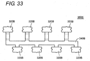
Fig. 33 is a view showing a variant of the rigid flexible substrate of the illuminating device; -
Figs. 34A and 34B are views for describing an auxiliary fixing member attached in the variant of the rigid flexible substrate of the illuminating device; -
Fig. 35 is a view for describing an example of a wiring pattern in the variant of the rigid flexible substrate of the illuminating device; -
Fig. 36 is a view for describing an example of a wiring pattern in the variant of the rigid flexible substrate of the illuminating device; -
Fig. 37 is a view showing a variant of the rigid flexible substrate of the illuminating device; -
Fig. 38 is a view showing a variant of the rigid flexible substrate of the illuminating device; -
Fig. 39 is a view showing a variant of the rigid flexible substrate of the illuminating device; -
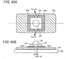
Figs. 40A and 40B are views for describing a mounting example of the light emitting element of the illuminating device; -
Fig. 41 is a schematic view showing a circuit configuration of a controller for lighting according to the embodiment of the present invention; -
Fig. 42 is a schematic view showing a circuit configuration of a controller for lighting according to the embodiment of the present invention; and -
Fig. 43 is a schematic View showing a circuit configuration of a controller for lighting according to the embodiment of the present invention. - Hereinafter, preferred embodiments of the present invention will be described with reference to the drawings. Like reference numerals are used to designate like or corresponding portions throughout the figures, and the description thereof will not be repeated.
- A manufacturing method for manufacturing an illuminating device present embodiment is used to manufacture a plurality of types of illuminating device having different size and specifications using a common substrate on which a light emitting element is to be mounted. The substrate is typically in a state of being wound around a reel, as hereinafter described, and is cut into a necessary length to create a substrate piece in a manufacturing process according to the size, specification, and the like of the illuminating device to be manufactured. The illuminating device is manufactured using the substrate piece.
- Therefore, a great number of variations (product groups) for the illumination field and the illumination distance can be lined up using the common substrate.
-
Fig. 1 is a schematic view showing an outline of a visual sensor system SYS using the illuminating device according to the present embodiment. With reference toFig. 1 , the visual sensor system SYS is typically incorporated in a production line and the like, and executes a process (hereinafter also referred to as a "measurement process") such as character recognition and scratch examination based on an image obtained by imaging an object to be examined (hereinafter also referred to as a "workpiece") W. - More specifically, the visual sensor system SYS includes an
image processing device 1, acamera 2 connected to theimage processing device 1, and an illuminating device 3 (in the following description, illuminatingdevices 3A to 3H are illustrated apart from the present embodiment) for illuminating the field range and the vicinity of thecamera 2. Thecamera 2 images the workpiece W transported on theproduction line 4 at an appropriate timing to generate image data, and outputs the generated image data to theimage processing device 1. - The
image processing device 1 is a computer including a CPU (Central Processing Unit), a memory, and the like, and is integrally formed with a display for displaying measurement processing results and the like in the example shown inFig. 1 . - The illuminating
device 3 according to the present embodiment uses a light emitting element such as LED (Light Emitting Diode) as a light source. The LED serving as a light source of the illuminatingdevice 3 may be a shell type LED, a surface mounting chip LED, a bare chip mounting LED, and the like depending on the difference in shape, mounting mode and the like. In particular, the illuminating device according to the present embodiment is suitable when using the surface mounting chip LED or the bare chip mounting LED. - Although
Fig. 1 shows a configuration in which a ring-shaped (doughnut-shaped) illuminating device is attached to the periphery of thecamera 2, an illuminating device arranged in the vicinity of thecamera 2 may be adopted. In this case, the shape (outer shape, size, etc. of the light emitting portion) of the illuminating device also can be designed according to the application. - The line up of the illuminating device that can be manufactured through the manufacturing method will now be described.
Figs. 2 to 9 are views showing the outer appearance of the illuminating device according to the present embodiment. -
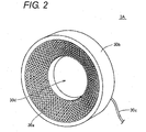
Fig. 2 shows a direct ringtype illuminating device 3A as one example of the illuminating device according to the present embodiment. The illuminatingdevice 3A has a bowl shape, where a plurality oflight emitting elements 30a are arranged on the inner surface of ahousing 30b having acircular void portion 30d formed at the center part. More specifically, the inner surface of thehousing 30b is formed to be inclined toward the center part, and thelight emitting elements 30a are arranged in a line at a predetermined interval on the inclined inner surface. Thevoid portion 30d is a hole for thecamera 2 to pass through to be arranged as shown inFig. 1 . - The power for turning ON the
light emitting element 30a is supplied by asupply line 30c. The entirelight emitting elements 30a may be driven to be turned ON/OFF all together, but thelight emitting elements 30a on each circumference arranged in order from the center part toward the outer periphery may be independently driven. In other words, one group of light emittingelements 30a arranged on the circumference positioned on the inner periphery side and one group of light emittingelements 30a arranged on the circumference positioned on the outer periphery side may be respectively turned ON/driven at independent timing to more appropriately illuminate the workpiece W. -
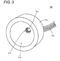
Fig. 3 shows a dometype illuminating device 3B as one example of the illuminating device according to the present embodiment. In the illuminatingdevice 3B,light emitting elements 31a are arranged at the lower part in the dome (bottom of inner surface side) of ahousing 31b which inner surface has a dome (semispherical) shape. More specifically, astorage space 31d for storing thelight emitting elements 31a is formed at the lower part in the dome of thehousing 31b, and thelight emitting elements 31a are arranged over the entire periphery of thestorage space 31d. The light emitted from thelight emitting elements 31a is diffusely reflected at a diffusereflection surface 31e formed on the inner surface of thehousing 31b, and then applied on the workpiece. The power for lighting suchlight emitting elements 31a is supplied by asupply line 31c. -
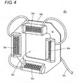
Fig. 4 shows a square oblique light type illuminating device 3C as one example of the illuminating device according to the present embodiment. The illuminating device 3C has light emitting units arranged on anoctagonal base plate 32b in which four square corners are cutout, where the light emitting units havelight emitting elements 32a arranged in a line at positions corresponding to four sides of the square. A substantially squarevoid portion 32d is formed at the center portion of thebase plate 32b. Thecamera 2 may be passed through and arranged at thevoid portion 32d for use. - Each light emitting unit is deflection arranged so as to face the center portion of the
base plate 32b. With this arrangement, the workpiece W arranged on a center axis of thebase plate 32b can be irradiated with the light emitted from each light emittingelement 32a, - The power for lighting the
light emitting elements 32a is supplied by asupply line 32c. The entire light emitting elements may be driven to be turned ON/OFF all together, but may be independently driven in units of light emitting units. The workpiece W then can be more appropriately illuminated. -
Fig. 5 shows a bar/linetype illuminating device 3D as one example of the illuminating device according to the present embodiment. The illuminatingdevice 3D has a plurality oflight emitting elements 33a arranged in a line in predetermined direction in arectangular housing 33b. An example in which thelight emitting elements 33a are arranged in a line over three columns is shown inFig. 5 , but may be arranged over one column or two columns, or thelight emitting elements 33a may be arranged in a line over greater number of columns. The bar/linetype illuminating device 3D is typically arranged such that the longitudinal direction thereof is parallel to or perpendicular to a transporting direction of theproduction line 4. - The power for lighting the
light emitting elements 33a is supplied by a supply line 33c. The entirelight emitting elements 33a may be driven to be turned ON/OFF all together, but may be independently driven in units of columns. The workpiece W then can be more appropriately illuminated. -
Fig. 6 shows a directly belowtype illuminating device 3E as one example of the illuminating device according to the present embodiment. The illuminatingdevice 3E has a plurality of light emitting elements (not shown) arranged in a line on a surface of a substantiallysquare housing 34b, and adiffusion transmission unit 34a arranged to cover the light emitting surfaces of the light emitting elements. The light emitted from the plurality of light emitting elements is thus diffused by thediffusion transmission unit 34a to illuminate the workpiece. The power for lighting the light emitting elements is supplied by asupply line 34c. -
Figs. 7A and 7B show a ringtype illuminating device 3F mounted with eight LEDs as one example of the illuminating device according to the present embodiment.Fig. 7A shows the irradiation surface side of the illuminatingdevice 3F, andFig. 7B shows the rear surface side of the illuminatingdevice 3F. - As shown in
Figs. 7A and 7B , the illuminatingdevice 3F has a ring shape as a whole More specifically, the illuminatingdevice 3F includes a base 100 corresponding to a first housing, and acase 500 corresponding to a second housing. As hereinafter described, thebase 100 and thecase 500 are configured as an integrated ring shape by being fitted to each other by snap-fit arid the like. - A plurality of
lenses 200 are concentrically arranged on the irradiation surface of the base 100 so as to be exposed. The irradiation surface of thebase 100 is formed as an inclined surface having a predetermined angle with respect to a center axis of acenter hole 700 formed to pass through thebase 100 and thecase 500. - A unit substrate mounted with light emitting elements in correspondence with the
respective lenses 200 is arranged in thecase 500, and apower supply cable 600 for supplying power to the light emitting elements is attached through a cutout formed at the side surface of thecase 500. - The illuminating
device 3F in which eight lenses are attached on the irradiation surface is illustrated inFigs. 7A and 7B , but instead of such a configuration, a configuration in which a greater number of lenses or a lesser number of lenses is attached may be adopted. -
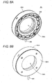
Fig. 8A andFig. 9B show the irradiation surface side of illuminatingdevices Fig. 8B andFig. 9B show the rear surface side of the illuminatingdevices - As shown in
Figs. 8A and 8B , a configuration in which a greater number of lenses 200 (and light emitting elements) is attached in comparison with the illuminatingdevice 3F shown inFigs. 7A and 7B may be adopted. In the example shown inFigs. 8A and 8B , the diameter of acenter hole 700A is basically greater than the diameter of thecenter hole 700 of the illuminatingdevice 3F shown inFigs. 7A and 7B . However, thelenses 200 same as thelenses 200 used in the illuminatingdevice 3F shown inFigs. 7A and 7B may be used. - On the other hand, as shown in
Figs. 9A and 9B , a configuration in which a lesser number of lenses 200 (and light emitting elements) is attached in comparison with the illuminatingdevice 3F shown inFigs. 7A and 7B may be adopted. In the example shown inFigs. 9A and 9B , the diameter of acenter hole 700B is basically smaller than the diameter of thecenter hole 700 of the illuminatingdevice 3F shown inFigs. 7A and 7B . However, thelenses 200 same as thelenses 200 used in the illuminatingdevice 3F shown inFigs. 7A and 7B may be used. - The basic structure for manufacturing the illuminating device will now be described.
-
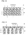
Fig. 10 is a schematic view showing asubstrate 10 for manufacturing the illuminating device. With reference toFig. 10 , thesubstrate 10 shown inFig. 10 is a so-called flexible printed substrate (hereinafter also referred to as a "flexible substrate") as a whole, and is formed with light emitting elements (LED) and wiring etc. for supplying power to the light emitting elements. More specifically, thesubstrate 10 has a conductor foil indicating the wiring pattern formed on a film-like insulator (base film), and then is covered with an insulator. - In particular, the
substrate 10 is formed with abent portion 16 along the long side direction at a predetermined position in the short side direction. In other words, thesubstrate 10 can be divided to acommon portion 10A and anindividual portion 10B where the relative positional relationship therebetween changes by thebent portion 16. Thecommon portion 10A and theindividual portion 10B are both made of flexible substrate. - In the
individual portion 10B, separatingportions 15 are formed along the short side direction at every predetermined interval in the long side direction. The separatingportions 15 separate theindividual portion 10B tounits 14 for every predetermined interval in the long side direction. In other words, it can be assumed as a plurality of reed-shapedunits 14 coupled to onecommon portion 10A. By way of example, each of the separatingportions 15 is realized by forming a perforated line (holes at a predetermined interval) on thesubstrate 10. - Two or more
light emitting elements 13 for emitting light are mounted on eachunit 14. More specifically, thelight emitting elements 13 are mounted on a predetermined position of the unit 14 (individual portion 10B) by surface mounting or bare chip mounting. Furthermore, the lens may be mounted in correspondence with each light emittingelement 13. - The
common portion 10A is a member for supplying power to thelight emitting elements 13 mounted on eachunit 14, where an electrode extending along the long side direction is formed andconductive pads 12 are formed at every predetermined interval. As hereinafter described, when an arbitrary number ofunits 14 is separated as one unit, each of thepads 12 becomes the portion for supplying power to the separated substrate piece. Eachpad 12 is thus arranged on or near the extended line of the corresponding separatingportion 15. - Furthermore, a
wiring 17 connected in series with thefight emitting elements 13 mounted on eachindividual portion 10B is formed between thecommon portion 10A and theindividual portion 10B. In other words, with regards to eachindividual portion 10B, thewiring 17 electrically connects thecorresponding pad 12 of thecommon portion 10A and the firstlight emitting element 13, and sequentially connects the firstlight emitting element 13 and the adjacentlight emitting element 13 in series. Thewiring 17 electrically connects the lastlight emitting element 13 and thepad 12 corresponding to theunit 14 adjacent to its unit. - With such a wiring structure, the
pads 12 exist at both ends of each separated substrate piece and all thelight emitting elements 13 included in the relevant substrate piece can be driven by simply applying a predetermined voltage between twopads 12 regardless of along which separatingportion 15 thesubstrate 10 is separated. - As described above, the
substrate 10 is made from a soft and bendable raw material. Furthermore, thesubstrate 10 is formed with a wiring that can supply power over a plurality oflight emitting elements 13. The substrate can be folded between thecommon portion 10A and theindividual portion 10B, where theindividual portion 10B configures the reed-shapedunits 14 on which thelight emitting elements 13 can be mounted on at least one surface. In theindividual portion 10B, the reed-shapedunits 14 each having the same shape and structure are repeatedly continued. - As hereinafter described, the illuminating device of various modes can be manufactured by shaping the
common portion 10A to a target shape. Thesubstrate 10 is typically handled in a state of being wound around the reel, and is pulled out and cut into units of necessary length. Such a manufacturing method is adaptable to the case of continuously manufacturing the same type of illuminating device and the case of manufacturing a wide variety of illuminating devices. Thesubstrate 10 has thepad 12 arranged on the extended line of the separatingportion 15 for separating theadjacent units 14, and hence the power can be supplied from both end sides of the cutcommon portion 10A as long as in units of multiples of theunit 14 even if the substrate is cut at any length. -
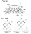
Fig. 11 is a schematic view showing asubstrate 20 of another mode for manufacturing the illuminating device. With reference toFig. 11 , thesubstrate 20 includes acommon portion 20A which is a flexible substrate, and an individual portion 20B connected to thecommon portion 20A. The individual portion 20B includes a plurality ofunits 24, where two or more light emitting elements (LED) 23 for emitting light are mounted on eachunit 24. Eachunit 24 is made of a material (typically, glass epoxy substrate) harder than the material of thecommon portion 20A. The mounting of thelight emitting elements 23 to eachunit 24 is thereby facilitated. Thelight emitting elements 23 are mounted at a predetermined position of the unit 24 (individual portion 20B) by surface mounting or bare chip mounting. Furthermore, the lens may be mounted in correspondence with each light emittingelement 23. - More specifically, the
common portion 20A has a plane shape as if a T-shape is continued, where the substrate configuring theunit 24 is electrically and mechanically joined to each of T-shapedportions 21. - The
substrate 20 is formed with thebent portion 26 along the long side direction at each T-shapedportion 21. In other words, the relative positional relationship between thecommon portion 20A and the individual portion 20B can be changed with thebent portion 26 as a center. - The
common portion 20A is a member for supplying power to thelight emitting elements 23 mounted on eachunit 24, where an electrode extending along the long side direction is formed andconductive pads 22 each are formed at substantially an intermediate position of the two adjacent T-shapedportions 21. As hereinafter described, thepad 22 becomes the portion for supplying power to the separated substrate piece when separated with an arbitrary number ofunits 24. - A
wiring 27 connected in series with thelight emitting elements 23 mounted on each individual portion 20B is formed between thecommon portion 20A and the individual portion 20B. Similar to thewiring 17 shown inFig. 10 , thewiring 27 supplies power over a plurality oflight emitting elements 23. - With such a wiring structure, the
substrate 20 can be separated along one of thepads 22, so that all thelight emitting elements 23 included in the substrate piece can be driven by simply applying a predetermined voltage between twopads 22 that exist at both ends of each separated substrate piece. - As described above, the
common portion 20A of thesubstrate 20 is made from a soft and bendable raw material. The individual portion 20B of thesubstrate 20 is made from a harder raw material that facilitates the mounting of thelight emitting element 23. The substrate can be folded between thecommon portion 20A and the individual portion 20B, where the individual portion 20B configures the reed-shapedunit 24 on which thelight emitting elements 23 are mounted on at least one surface. Therefore, the illuminating device of various modes can be manufactured by shaping thecommon portion 20A to a target shape. - The
substrate 20 is typically handled in a state of being wound around the reel, and is pulled out and cut into units of necessary length. Such a manufacturing method is adaptable to the case of continuously manufacturing the same type of illuminating device and the case of manufacturing a wide variety of illuminating devices. -
Fig. 12 to Fig. 15 are views for describing the manufacturing process of the illuminating device. In particular,Fig. 12 shows the first process of creating a necessary substrate piece,Fig. 13 shows the second process of forming the created substrate piece,Fig. 14 shows the third process of physically connecting the formed substrate piece to the housing, andFig. 15 shows the fourth process of electrically connecting the formed substrate piece connected to the housing. In the example shown inFigs. 12 to 15 , the manufacturing process used in manufacturing the illuminating device using thesubstrate 10 shown inFig. 10 is shown by way of example, but the similar manufacturing process can be adopted when using thesubstrate 20 shown inFig. 11 . - First, as shown in
Fig. 12 , thesubstrate 10 in a state, of being wound around the reel is sent out at a predetermined speed and the light emitting elements 13 (chip LEDs) are sequentially mounted at a predetermined position of thesubstrate 10 using a robot 7. Thesubstrate 10 mounted with thelight emitting elements 13 is then cut into units of length (necessary number of units 14) corresponding to the illuminating device to be manufactured using acutter 8 having a blade parallel to the short side direction of thesubstrate 10. - In other words, in the first process, the
substrate 10 mounted with thelight emitting elements 13 is Cut in the first direction (short side direction) to create the substrate piece. As described above, thesubstrate 10 includes a first portion (common portion 10A) having flexibility, and a plurality of second portions (individual portion 20B/unit 14) that can be bent with respect to the first portion. The first portion (common portion 10A) extends in the second direction (long side direction) orthogonal to the first direction (short side direction), and includes pads arranged at every interval defined in advance in the second direction (long side direction). Eachunit 14 is connected to the first portion (common portion) between twocontinuous pads 12, and includes awiring 17 for electrically connecting the terminals of the mountedlight emitting elements 13 and the two correspondingpads 12. - More specifically, a command is given to the
cutter 8 to cut at a timing the necessary number ofunits 14 exist on the right side in the plane of drawing than the blade of thecutter 8 since thesubstrate 10 is sent out at a predetermined speed. In this case, the alignment process is performed so that one of the separatingportions 15 of thesubstrate 10 and the position of the blade of thecutter 8 coincide with each other. More specifically, the chip LEDs are first mounted as the light emitting elements on thesubstrate 10, and then thesubstrate 10 is cut into an appropriate length at the position of the separatingportion 15. In other words, the cutting length is changed according to the shape of the illuminating device to be manufactured. - The
substrate 10 is cut in the short side direction at the position where thepad 12 exists. - The cutting of the
substrate 10 does not necessarily need to be automated, and may be manually realized. - As shown in
Fig. 13 , the substrate piece of thesubstrate 10 created by cutting forms thecommon portion 10A to a shape corresponding to the illuminating device to be manufactured. In the example shown inFig. 13 , an example of forming thecommon portion 10A to a circular shape (ring shape) is shown, but the cross-sectional shape may be polygonal or an ellipse. Thecommon portion 10A is typically a flexible substrate and can be easily formed to a shape corresponding to the illuminating device to be manufactured. - As shown in
Fig. 14 , the substrate piece of the formedsubstrate 10 is physically connected to thehousing 50. Thehousing 50 shown inFig. 14 is used when manufacturing the direct ring type illuminating device shown inFig. 2 and the like, where the inner surface thereof is formed into a bowl shape and a circular void portion is formed at the center part thereof. The substrate piece of the formedsubstrate 10 is physically joined to the inclined portion etc. of the inner surface of thehousing 50. In this case, the substrate piece of thesubstrate 10 and thehousing 50 are fixed using a lock member such as a screw, an auxiliary member for sandwiching the substrate piece of thesubstrate 10 and thehousing 50, and the like. - In other words, the
common portion 10A is fixed to thehousing 50 and the relative position of theindividual portion 10B (each unit 14) with respect to thecommon portion 10A is respectively positioned. - After the substrate piece of the
substrate 10 is fixed to thehousing 50, the drive circuit substrate arranged inside or at a proximate position of thehousing 50 and the substrate piece of thesubstrate 10 are electrically connected. In other words, the wiring for supplying power to thepad 12 arranged in the substrate piece of thesubstrate 10 is formed. -
Fig. 15 shows a cross-sectional view taken along line XI-XI ofFig. 14 . By way of example, thedrive circuit substrates 52 for lighting thelight emitting elements 13 are arranged at the upper side inside thehousing 50, and thedrive circuit substrates 52 and the pair ofpads 12 in the substrate piece of thesubstrate 10 are electrically connected through alead wire 56, as shown inFig. 15 . Each of thedrive circuit substrates 52 is formed into a cylindrical shape, and is mounted with a drive circuit 54 (transistor etc.) for driving the light emitting element at a predetermined position. The power is externally supplied to thedrive circuit substrate 52 through alead wire 58. - As shown in
Fig. 15 , thelight emitting elements 13 are mounted on the substrate piece of thesubstrate 10 with the lower side in the plane of drawing corresponded to the surface that can irradiate when attached to thehousing 50. An example in which the substrate piece of thesubstrate 10 is fixed to thehousing 50 while thedrive circuit substrate 52 is incorporated in advance inside thehousing 50 is shown, but thedrive circuit substrate 52 may be prepared exterior to thehousing 50 and the power may be directly supplied from such an externaldrive circuit substrate 52 to the substrate piece of thesubstrate 10. - The illuminating device is basically manufactured through the procedures shown in
Figs. 12 to 15 . Thus, the illuminating device can be manufactured by mounting the light emitting elements (chip LEDs) on each reed-shaped unit and forming only thecommon portion 10A in the substrate piece of thesubstrate 10 to the target shape. Therefore, the illuminating device having various complex shapes can be realized without imposing a mechanical stress on the mounted light emitting element (chip LED). - One example, of the illuminating device manufactured through the manufacturing method described above will now be described.
-
Figs. 16A to 16C are views for describing the direct ring type illuminating device manufactured using the manufacturing method. That is,Figs. 16A to 16C shows one example of a process used in manufacturing a direct ringtype illuminating device 3A as shown inFig. 2 . - A great number of variations (product groups) for the illumination field and the illumination distance need to be lined up for the direct ring type illuminating device as shown in
Fig. 2 according to the field range etc. of the size of thecamera 2 to be coupled. According to the manufacturing method, the size of the substrate piece to use for the illuminating device, that is, the number ofunits 14 to be arranged in one substrate piece can be arbitrarily set, and the shape of thecommon portion 10A in the substrate piece can also be an arbitrary shape. - As shown in
Figs. 16A to 16C , the number ofunits 14 to be arranged in the substrate piece, the shape of thecommon portion 10A (e.g., radius when forming to a ring shape, etc.) and the like can be freely changed according to the diameter of the void portion, the size (area) of the irradiation surface, the irradiation angle, and the like of the direct ring type illuminating device to be manufactured. - Various direct ring type illuminating devices then can be manufactured using the
common substrate 10. -
Figs. 17A and 17B are views for describing a direct ring type illuminating device with enhanced illumination intensity manufactured using the manufacturing method. In particular,Fig. 17A shows the positional relationship of two shaped substrate pieces 10-1 and 10-2, andFig. 17B shows the illumination range of the present illuminating device. - As shown in
Fig. 17A , a plurality of (two in the example ofFigs. 17A and 17B ) substrate pieces 10-1 and 10-2 are formed into a similar structure, and then the two substrate pieces 10-1 and 10-2 are arranged in a shifted manner so that the irradiation positions of respective light emitting elements 13-1 and 13-2 do not overlap. With this, the illumination intensity can be enhanced compared to when one substrate piece is used. In other words, the substrate pieces 10-1 and 10-2 are arranged with the relative angle in between differed on the common optical axis. - In other words, a plurality of substrate pieces are created from the
common substrate 10, and each of the substrate pieces is formed according to the illuminating device to be manufactured. Furthermore, the formed plurality of substrate pieces are fixed in a predefined positional relationship. - As shown in
Fig. 17B , the substrate pieces 10-1 and 10-2 are both configured to substantially the same shape, so that the range (illumination ranges 1 and 2) irradiated with light from each substrate piece (light emitting element) substantially coincide. Therefore, the irradiation intensity in the common illumination range can be enhanced by fixing two substrate pieces (arraying on the same optical axis AX) to the same housing. -
Figs. 18A and 18B are views for describing the direct ring type illuminating device in which the illumination range is further adjusted using the manufacturing method. In particular,Fig. 18A shows the positional relationship of the two shaped substrate pieces 10-1 and 10-2, andFig. 18B shows the illumination range of the present illuminating device. - As shown in
Fig. 18A , a plurality of (two in the example ofFigs. 18A and 18B ) substrate pieces 10-1 and 10-2 are formed into a similar structure, and then the two substrate pieces 10-1 and 10-2 are arranged in a shifted manner in the up and down direction in the plane of drawing so that the illumination range can be enlarged compared to when one substrate piece is used. In other words, the substrate piece 10-1 and the substrate piece 10-2 are arranged on the common optical axis separated by a predetermined distance. - In other words, a plurality of substrate pieces are created from the
common substrate 10, and each of the substrate pieces is formed according to the illuminating device to be manufactured. Furthermore, the formed plurality of substrate pieces are fixed in a predefined positional relationship. - As shown in
Fig. 18B , the substrate pieces 10-1 and 10-2 are both configured to substantially the same shape, and thus the irradiation angle of the light emitted from the light emitting elements mounted on each substrate piece substantially coincides. However, theillumination range 1 illuminated by the light emitting element 13-1 mounted on the substrate piece 10-1 is a circular range having the optical axis AX as the center where as theillumination range 2 illuminated by the light emitting element 13-2 mounted on the substrate piece 10-2 is a concentric (doughnut-shaped) range having the optical axis AX as the center since the distance from each substrate piece to the subject differs. Therefore, the illumination range of the illuminating device becomes a range corresponding to the sum of therumination range 1 and theillumination range 2 shown inFig. 18B by fixing two substrate pieces to the same housing. In other words, the illumination range can be enlarged compared to when one substrate piece is used. -
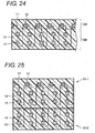
Figs. 19A and 19B are views for describing the direct ring type illuminating device in which the illumination range can be changed manufactured using the manufacturing method. In particular,Fig. 19A shows a structure of the present illuminating device, andFig. 19B shows the illumination range of the present illuminating device. - As shown in
Fig. 19A , a mechanism (focus mechanism) for varying the relative positional relationship between thecommon portion 10A and theindividual portion 10B is added with respect to the substrate piece of thesubstrate 10 in which thecommon portion 10A is shaped to a ring shape. In other words, a mechanism in which the relative position of theindividual portion 10B with respect to thecommon portion 10A can be changed is added. - Although an arbitrary structure can be adopted for such a focus mechanism, a configuration in which a housing including two members relatively movable along a common axis is prepared where one member is fixed to the
common portion 10A and the other member is fixed to theindividual portion 10B may be adopted, so that the angel of theindividual portion 10B with respect to thecommon portion 10A can be changed. The range in which the most appropriate illumination intensity is generated can be changed as shown inFig. 19B by changing the angle between thecommon portion 10A and theindividual portion 10B. - For example, when the angle between the
common portion 10A and theindividual portion 10B is θ1, the illumination range of substantially an even illumination intensity can be realized if the distance between the illuminating device and the subject is L1, and when the angle between thecommon portion 10A and theindividual portion 10B is θ2, the illumination range of substantially an even illumination intensity can be realized if the distance between the illuminating device and the subject is L2. In other words, the distances L1, L2 are the illumination distances of the illumination device, and the illumination distance of the illuminating device can be changed in the range from L1 to L2 by changing the angle between thecommon portion 10A and theindividual portion 10B from θ1 to θ2. -
Figs. 20A and 20B are views for describing the direct ring type illuminating device in which the illumination intensity is evened manufactured using the manufacturing method. In particular,Fig. 20A shows the structure of the present illuminating device, andFig. 20B shows the illumination range of the present illuminating device. - In the substrate piece of the
substrate 10 shown inFig. 20A , the LEDs with lenses having different irradiation fields are used for the light emitting element 13-1 mounted on the inner side and the light emitting element 13-2 mounted on the outer side. - More specifically, the LED having a relatively narrow irradiation field is adopted for the light emitting element 13-1 on the inner side and the LED having a relatively wide irradiation field is adopted for the light emitting element 13-2 on the outer side. The illumination intensity of the illumination range can be evened by having the irradiation fields in such a manner.
- For example, as shown in
Fig. 20B , the light emitting element 13-1 on the inner side illuminates a narrower range having the optical axis AX corresponding to the center axis of the substrate piece of thesubstrate 10 as the center since the illumination field is relatively narrow, and the light emitting element 13-2 on the outer side illuminates a wider range having the optical axis AX corresponding to the center axis of the substrate piece of thesubstrate 10 as the center since the illumination field is relatively wide. Thus, the illumination intensity possibility lowers on the outer peripheral side of the illumination range by the light emitting element 13-1 on the inner side, but such lowering of the illumination intensity can be compensated with the illumination light emitted from the light emitting element 13-2 o the outer side. Therefore, the illumination intensity in the illumination range can be evened. - Japanese Unexamined Patent Publication No.
2002-94129 -
Fig. 21 is a view for describing the direct ring type illuminating device in which stray light to the camera is reduced manufactured using the manufacturing method. - In the example of the illuminating device described above, a configuration such that the angle of the
individual portion 10B with respect to thecommon portion 10A is a blunt angle has been described, but the stray light to thecamera 2, to which the illuminating device is attached, can be reduced by configuring such that the angle of theindividual portion 10B with respect to thecommon portion 10A is an acute angle. In other words, the light emitted from thelight emitting element 13 mounted on theindividual portion 10B is suppressed from directly entering thecamera 2 due to the presence of thecommon portion 10A, as shown inFig. 21 . - The appearing of the illumination light in the image data generated by the imaging of the
camera 2, the occurrence of unintended halation, and the like can be avoided by suppressing such stray light. -
Figs. 22A and 22B are views for describing the dome type illuminating device manufactured using the A manufacturing method. In other words;Fig. 22A shows an example of a process for manufacturing the dome type illuminating device using one substrate piece, andFig. 22B shows an example of a process for manufacturing the dome type illuminating device using a plurality of substrate pieces. - When manufacturing the dome type illuminating device as showh in
Fig. 3 , the irradiation surface becomes relatively wide and the curvature radius becomes relatively small. Therefore, the irradiation surface of smaller curvature radius can be realized by further bending eachunit 14 in the structure shown inFig. 22A , and the irradiation surface of smaller curvature radius can be realized by stereoscopically arranging a plurality ofunits 14 in the structure shown inFig. 22B . - More specifically, a
bent portion 19 is formed at the portion where the light emitting element does not exist in eachindividual portion 10B (unit 14) connected to thecommon portion 10A in the illuminating device shown inFig. 22A . The emitting direction of each light emitting element is changed by bending eachunit 14 at thebent portion 19. The illumination light of even intensity then can be emitted from the inner surface. - The illuminating device shown in
Fig. 22B is configured by the substrate piece 10-1 formed so that the common portion has a certain radius, and the substrate piece 10-2 formed to have a radius smaller than the radius of the common portion of the substrate piece 10-1. The substrate piece 10-1 and the substrate piece 10-2 are then stereoscopically arranged. In other words, the substrate piece 10-2 is arranged so that the unit 14-2 is positioned on the inner side of the center portion of the substrate piece 10-1. The units 14-1 and 14-2 in which the light emitting element is mounted then can be arranged along the dome shape on the inner side by stereoscopically arranging the two substrate pieces. -
Fig. 23 is a view for describing a square oblique light type illuminating device manufactured using the manufacturing method. - As shown in
Fig. 23 , the substrate piece is prepared according to the number of directions (four directions in the example shown inFig. 23 ) the illumination light is applied when A manufacturing the square oblique type illuminating device (seeFig. 4 ). In this case, thecommon portion 10A does not need to be formed into a circular shape as in the direct ring type described above, and a substrate piece including a predetermined number ofunits 14 may be prepared, the common portion of the substrate piece may be fixed to each surface of the rectangular housing, and the angle of theindividual portion 10B with respect to thecommon portion 10A may be adjusted to a target value. - Therefore, when manufacturing the square oblique light type illuminating device, the number of
units 14 included in each substrate piece is adjusted and the angle of theindividual portion 10B with respect to thecommon portion 10A is adjusted in each substrate piece according to the size (housing size and length of irradiation surface) to realize the target specification. - Various square oblique light type illuminating devices then can be manufactured using the
common substrate 10. -
Fig. 24 is a view for describing a process for A manufacturing a bar/line type illuminating device using the manufacturing method. - As shown in
Fig. 24 , the substrate piece including a number ofunits 14 corresponding to the size of the irradiation surface is prepared when manufacturing the bar/line type illuminating device (seeFig. 5 ). In this case, thecommon portion 10A does not need to be formed into a circular shape and theunits 14 do not need to be separated as in the direct ring type described above. As shown inFig. 12 , basically, thesubstrate 10 in a state of being wound around the reel is merely cut into a target length and the cut substrate piece is fixed to the housing. In this case, the separating portion 15 (seeFig. 10 ) for separating theunits 14 is not necessary, and hence the separatingportion 15 may not be formed. - Various bar/line type illuminating devices can be manufactured by adjusting the length to cut from the
common substrate 10. -
Fig. 25 is a view for describing a process for manufacturing a directly below type illuminating device using the manufacturing method. - The directly below type illuminating device as shown in
Fig. 6 needs to have the irradiation surface formed relatively large. The length in the long side direction of thesubstrate 10 can be arbitrarily set, but the length in the short side direction of the substrate 10 (range in which thelight emitting elements 13 are mounted in the unit 14) may become insufficient. A sufficient irradiation area is thus ensured by arranging a plurality of substrate pieces in a line in the short side direction, as shown inFig. 25 . - In other words, when manufacturing the directly below type illuminating device, the substrate pieces 10-1 and 10-2 each including a number of
units 14 corresponding to the size of the irradiation surface are prepared. The substrate pieces 10-1 and 10-2 arranged in parallel are then mounted on the housing to manufacture the directly below type illuminating device. The overlapping portion of the substrate piece 10-1 and the substrate piece 10-2 is stereoscopically arranged. In other words, one substrate piece is arranged on the upper side and the other substrate piece is arranged on the lower side with an insulating layer and the like arranged between the substrate pieces. A wider irradiation surface can then be realized. - Various directly below type illuminating devices then can be manufactured by adjusting the length to cut from the
common substrate 10. - The structure of a substrate in which the number of columns of the light emitting elements can be changed will now be described. In other words, a substrate structure in which the length of the reed-shaped unit can be changed is illustrated.
-
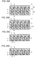
Figs. 26A to 26D are schematic views showing a substrate of a mode for manufacturing the illuminating device according to the present embodiment. In particular,Fig. 26A shows the basic structure of thesubstrate 30,Figs. 26B and 26C show a process of changing the length of the unit, andFig. 26D shows a process of decimating the light emitting element to mount. - With reference to
Fig. 26A , the basic structure of thesubstrate 30 is similar to thesubstrate 10 shown inFig. 10 . In other words, thesubstrate 30 includes acommon portion 30A configured by a flexible substrate, and the like, and an individual portion 30B (units 34) on which thelight emitting element 33 is mounted. Awiring 37 connected in series with thelight emitting elements 33 mounted on eachunit 34 is formed between thecommon portion 30A and the individual portion 30B. - In particular, by-
pass terminals 38 for electrically by-passing the light emitting element positioned the second in eachunit 34 are formed in thesubstrate 30. In other words, each by-pass terminal 38 short circuits the exit side wiring of the light emitting element positioned the first and the exit side wiring of the light emitting element positioned the second in the correspondingunit 34. It is in an electrically non-connecting state at the time of original formation. - In other words, in the individual portion 30B (units 34), the
wiring 37 is formed to mount a plurality oflight emitting elements 33 in series, and a wiring for by-passing thelight emitting element 33 positioned in the middle and thecorresponding pad 32 connected in series is formed. - As shown in
Fig. 26B , a case of cutting eachunit 34 of thesubstrate 30 before the by-pass terminal 38 is considered. In other words, when manufacturing a smaller device of the direct ring type illuminating devices described above, a fewer number oflight emitting elements 33 may be simply mounted on eachunit 34. - Thus, the portion where the
light emitting elements 33 are mounted in eachunit 34 is shortened as shown inFig. 26B , and ashort circuit member 39 is added to the by-pass terminal 38 of eachunit 34 as shown inFig. 26C . The power then can be supplied to thelight emitting elements 33 mounted on eachunit 34 through thewiring 37 electrically connected to thepad 32 even if the length of eachunit 34 is shortened. Theshort circuit member 39 is a conductive member having a small resistance value that can be assumed as a substantially 0 Ω. - In other words, the
substrate 30 is cut in the first direction (short side direction), and thereafter one part of the individual portion 30B (unit 34) included in the substrate piece obtained by cutting is cut in the second direction (long side direction) and the cut wiring is electrically connected with thecorresponding pad 32. - Furthermore, as shown in
Fig. 26D , the interval at which thelight emitting elements 33 are mounted can be decimated by mounting theshort circuit member 31 instead of mounting thelight emitting element 33. In other words, in the example shown inFig. 26D , theunit 34 mounted with thelight emitting elements 33 is alternately provided, so that the mounting density of the light emitting element becomes substantially 1/2. Therefore, the pitch of the substrate piece can be substantially adjusted by mounting theshort circuit member 31. - Therefore, a plurality of types of illuminating devices in which the mounting density of the
light emitting element 33 is changed can be manufactured using thesubstrate 30 shown inFigs. 26A to 26D : - An example of a case where the ring type illuminating device is configured using the substrate (basic structure II) shown in
Fig. 11 will be described below. -
Fig. 27 is an exploded perspective view of an illuminatingdevice 3F. - With reference to
Fig. 27 , thelenses 200 are attached from the rear surface side of the ring-shapedbase 100 in the illuminatingdevice 3F. A window to which thelenses 200 are attached in thebase 100 includes a holding portion for holding thelenses 200 arid regulating the movement of thelenses 200 toward the irradiation surface (exposed surface) side of thebase 100. - A concentrically formed rigid
flexible substrate 300 is arranged in correspondence with the arrangement form of thelenses 200. The rigidflexible substrate 300 includes a unit substrate mounted with a light emitting element corresponded to each of the plurality oflenses 200 arranged in a concentric form. The power for driving the fight emitting element is supplied to the rigidflexible substrate 300 through apower supply cable 600. - A substantially circular
heat dissipating sheet 400 for dissipating the heat generated in the light emitting elements of the rigidflexible substrate 300 is inserted between the rigidflexible substrate 300 and thecase 500. Theheat dissipating sheet 400 is made from a raw material having elasticity, and also functions as a buffer material or a pushing portion with respect to thelenses 200 and the rigidflexible substrate 300 inserted to a space between the base 100 and thecase 500. - The
case 500 is formed with projections for fixing each set including thelens 200 and the unit substrate mounted with the light emitting element at the surface on the base 100 side. - Each
lens 200 is positioned so that the optical axis thereof becomes substantially perpendicular to the irradiation surface of the base 100 at the arranged position. Thus, the optical axis of each of thelenses 200 is not parallel to the center axis of thecenter hole 700, and is held with a predetermined angle corresponding to the inclination angle of the irradiation surface. In other words, the optical axis of eachlens 200 is non-parallel with respect to the center axis of thecenter hole 700. The respective optical axes of thelenses 200 are also nonparallel. -
Figs. 28A and 28B are views for describing the configuration of the rigidflexible substrate 300 of the illuminatingdevice 3F. The rigidflexible substrate 300 shown inFigs. 28A and 28B is preferably adopted for thesubstrate 20 more suited for the illuminatingdevice 3F shown inFig. 27 . -
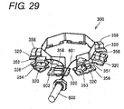
Fig. 28A is a view showing the rigidflexible substrate 300 immediate after manufacturing, andFig. 28B is a view showing a state of the rigidflexible substrate 300 before being incorporated to thebase 100.Fig. 29 is a view for describing the power supply method with respect to the rigidflexible substrate 300 of the illuminatingdevice 3F. - With reference to
Fig. 28A , the rigidflexible substrate 300 includes a number of unit substrates 320-1 to 320-8 (also collectively referred to as "unit substrates 320") corresponding to the number of thelenses 200 attached to thebase 100. Each of the unit substrates 320-1 to 320-8 is configured as an object (rigid body) made from a relatively hard material to perform positioning and fixation described above. Specifically, the unit substrates 320-1 to 320-8 are made of glass epoxy substrate. - The light emitting elements 330-1 to 330-8 (also collectively referred to as "
light emitting elements 330") for emitting light are respectively mounted on the glass epoxy substrates (unit substrates 320-1 to 320-8). More specifically, each of thelight emitting elements 330 is mounted at a predetermined position of each of theunit substrates 320 by surface mounting or bare chip mounting. Furthermore, a micro-lens is sometimes mounted in correspondence with each light emittingelement 330. The number of light emitting elements to be mounted on eachunit substrate 320 may be in plurals, and is appropriately set according to the design value (irradiation intensity) demanded on the illuminatingdevice 3F. - The substrate does not deform even if press fitted and fixed to the
base 100 and the light emitting element can be accurately positioned with respect to the lens as described above by using such a rigid substrate for theunit substrate 320. - The rigid
flexible substrate 300 includes a flexible printed substrate (hereinafter also referred to as a "flexible substrate") 340 for electrically connecting the unit substrates 320-1 to 320-8 (light emitting elements 330-1 to 330-8 mounted thereon). Theflexible substrate 340 is formed with a wiring etc. for supplying power to thelight emitting element 330. More specifically, theflexible substrate 340 has a conductor foil indicating the wiring pattern formed on the film-form insulator (base film), and further covered with an insulator. - In other words, the illuminating
device 3F incorporatesunit substrates 320 which are first substrates arranged in correspondence with the plurality oflenses 200. At least one light emitting element is mounted on eachunit substrate 320. Furthermore, the illuminatingdevice 3F incorporates theflexible substrate 340 for electrically connecting theunit substrates 320 which are the first substrates. Theunit substrate 320 is configured as a rigid body, and theflexible substrate 340 is configured to have flexibility. - As shown in
Fig. 28B , such a rigidflexible substrate 300 is incorporated in the base 100 after being concentrically formed as shown inFig. 28B . In other words, in theflexible substrate 340 of the rigidflexible substrate 300, aportion 340a linearly formed over a plurality ofunit substrates 320, and aportion 340b branched from theportion 340a to therespective unit substrates 320 are integrally configured. Theflexible substrate 340 is folded at the portion (seeFig. 28A ) indicated with a broken line of the linearly formedportion 340a, so that theflexible substrate 340 is shaped to a tortoise shell shape as shown inFig. 28B . Furthermore, theflexible substrate 340 is folded to the outer peripheral side at the portion (seeFig. 28A ) indicated with a broken line of theportion 340b branched to theunit substrate 320, so that the unit substrates 320-1 to 320-8 are formed to have a predetermined angle with respect to a plane defined by a substantially circular shape (tortoise shell shape) configured by theflexible substrate 340. When bending theflexible substrate 340, a polygonal shape shown inFig. 28B is preferable in relation with theunit substrate 320. In this case, the portion indicated with a wavy line ofFig. 28A is preferably processed to facilitate the folding. Theflexible substrate 340 may be bent to a circular shape. In such a case, it may not necessarily be folded at the portion indicated with a broken line inFig. 28A . - The
unit substrate 320 does not deform even if theflexible substrate 340 is bent as shown inFig. 28B by using the rigid substrate for theunit substrate 320. Therefore, stress does not apply on thelight emitting element 330 surface mounted on theunit substrate 320, and the reliability does not lower. - In the rigid
flexible substrate 300, a predetermined planar shape is formed along the circumferential direction of thebase 100 for theflexible substrate 340, and eachunit substrate 320 is bent at an angle corresponding to the tilt of thelens 200 held in a holding portion 110 of the base 100 with respect to the corresponding portion of the flexible substrate 340 (portion 340a linearly formed over a plurality of unit substrates 320). In other words, theflexible substrate 340 is bent along the line of a plurality of windows 102-1 to 102-8. - As will be described later, in the
flexible substrate 340, the wiring pattern is formed such that the light emitting elements 330-1 to 330-8 mounted on the unit substrates 320-1 to 320-8 are connected in series. Thus, the power is supplied between two points on the wiring path formed by theflexible substrate 340 including thelight emitting element 330, so that a group of light emitting elements 330-1 to 330-8 can be lighting driven. - More specifically, as shown in
Fig. 29 ,connectors unit substrates 320 positioned near the power supply cable 600 (power supply cable passing recess 150) that passes through thebase 100 and thecase 500 to be introduced inside of theunit substrates 320 configuring the rigidflexible substrate 300, andconnectors wirings power supply cable 600 are connected to theconnectors - The
connectors unit substrate 320. In other Words, the direction thewirings connectors power supply cable 600 to facilitate the pulling of thewirings power supply cable 600. In other words, theflexible substrate 340 includes a pair ofconnectors power supply cable 600 and the pair ofconnectors power supply cable 600. - As will be described later, a configuration in which a predetermined number of
light emitting elements 330 connected in series is connected in parallel by the necessary number may be adopted if the number oflight emitting elements 330 to be lighted is in great number. - A
circuit component 358 for driving thelight emitting element 330 is mounted on the surface on the side not mounted with thelight emitting element 330 in eachunit substrate 320. In other words, in eachunit substrate 320, the circuit components other than thelight emitting element 330 are basically mounted on the surface on the side opposite to the surface mounted with thelight emitting element 330. The space efficiency thus improves, and the substrate size of eachunit substrate 320 can be reduced. - As described with reference to
Fig. 27 , the rigidflexible substrate 300 is concentrically formed, and is then inserted between the base 100 corresponding to a first housing and thecase 500 corresponding to a second housing. At the time of the assembly task to the case, theflexible substrate 340 in the bent state may deform and bite into the base 100 corresponding to the first housing and thecase 500 corresponding to the second housing. In other words, theflexible substrate 340 may interfere with the base 100 or thecase 500 by collapsing to the inner side or the outer side from the original position. - Therefore, the assembly performance can be improved by using the auxiliary fixing member as shown in
Figs. 30A and 30B . -
Figs. 30A and 30B are views for describing the auxiliary fixing member attached to the rigid flexible substrate of the illuminating device.Fig. 30A shows a state in which the ring-shapedmember 360, which is the auxiliary fixing member, is attached with respect to the concentrically formed rigidflexible substrate 300, andFig. 30B shows a state of attaching the ring-shapedmember 360, which is the auxiliary fixing member, with respect to the concentrically formed rigidflexible substrate 300. - As shown in
Fig. 30B , the ring-shapedmember 360 is used for the auxiliary fixing member. The inner diameter of the ring-shaped member is designed to be greater than the circumscribed circle of the concentrically formedflexible substrate 340 by a predetermined margin. The ring-shapedmember 360 is attached to the outer peripheral side of the concentrically formedflexible substrate 340. The ring-shapedmember 360 is preferably formed with a material such as resin. - Therefore, the deformation (collapsing to the inner side or the outer side from the original position) of the
flexible substrate 340 can be prevented by supporting theflexible substrate 340 with the ring-shapedmember 360. An event in which theflexible substrate 340 bites between the base 100 corresponding to the first housing and thecase 500 corresponding to the second housing thus can be avoided. The assembly performance can be improved as a result. - An example of the wiring pattern in the rigid flexible substrate will be described below.
-
Fig. 31 andFig. 32 are views for describing the example of the wiring pattern in the rigid flexible substrate of the illuminating device.Fig. 31 shows an example in which eightlight emitting elements 330 are mounted on one rigid flexible substrate, andFig. 32 shows an example in which twelvelight emitting elements 330 are mounted on one rigid flexible substrate. In particular,Fig. 31 andFig. 32 show configuration examples in which the connectors related to power supply can be concentrated to one. - In the rigid
flexible substrate 330 shown inFig. 31 , asupply line 332 for connecting the light emitting elements 330-1 to 330-8 respectively mounted on the unit substrates 320-1 to 320-8 in series is formed on theflexible substrate 340. Both ends of thesupply line 332 are both connected to theconnector 356. Furthermore, they are connected to a controller for lighting thelight emitting element 330, as will be described later, through theconnector 356. In other words, the positive potential is supplied to one end of thesupply line 332 through theconnector 356, and the negative potential is supplied to the other end of thesupply line 332 through theconnector 356. - In the rigid
flexible substrate 300A shown inFig. 32 , the twelvelight emitting elements 330 are supplied with power in parallel six at a time using twosupply lines supply line 332A shown with a solid line inFig. 32 is formed to connect the odd numbered unit substrates 320-1, 320-3, 320-5, 320-7, 320-9, 320-11 in series, and thesupply line 332B shown with a broken line inFig. 32 is formed to pass through the even numbered unit substrates 320-2, 320-4, 320-6, 320-8, 320-10, 320-12 in series. - As hereinafter described, control is performed so that a constant current having a predetermined magnitude is supplied to the
light emitting element 330, and hence the supply current of therespective supply lines supply lines connector 356A, and the respective other ends of thesupply lines connector 356A. - Since the
supply line 332A and thesupply line 332B cannot be intersected while maintaining insulation on theflexible substrate 340, thesupply line 332A is generally formed on one surface of theflexible substrate 340, and thesupply line 332B is formed on the other surface of theflexible substrate 340. This example is shown inFig. 32B . - The configuration shown in
Fig. 33 to Fig. 36 may be adopted for the configuration of the rigid flexible substrate instead of the modes shown inFig. 28A to Fig. 32B . -
Fig. 33 is a view showing a variant of the rigid flexible substrate of the illuminatingdevice 3F.Figs. 34A and 34B are views for describing the auxiliary fixing member to be attached in the variant of the rigid flexible substrate of the illuminatingdevice 3F.Fig. 35 andFig. 36 are views for describing an example of the wiring pattern in the variant of the rigid flexible substrate of the illuminating device. - With reference to
Fig. 33 , the rigidflexible substrate 300B has a configuration in which the unit substrate 320A, on which thelight emitting element 330 is to be mounted, is arranged in a zigzag manner (alternate arrangement on both sides). The unit substrates 320B are connected through theflexible substrate 340B. Theflexible substrates 300B can be configured to a shape suited for incorporating to the base 100 as shown inFig. 29 by appropriately folding theflexible substrate 340B. - More specifically, the portion of the
flexible substrate 340B connected with theunit substrates 320B arranged on the upper side in the plane of drawing is long compared to the portion of theflexible substrate 340B connected with theunit substrates 320B arranged on the lower side in the plane of drawing. The unit substrates 320B arranged on the upper side in the plane of drawing are folded along the up and down direction in the plane of drawing to realize a structure similar to the rigidflexible substrate 300 shown inFig. 28A . In other words the fourunit substrates 320B arranged on the upper side in the plane of drawing are folded at the position indicated with a broken line, and theflexible substrate 340B is bent to a substantially circular shape (tortoise shell shape). Therefore, in theflexible substrate 340B, the surface on which thelight emitting element 330 is mounted on each of theunit substrates 320B positioned on the lower side in the plane of drawing and the surface oh which thelight emitting element 330 is mounted on each of theunit substrates 320B positioned on the upper side in the plane of drawing become opposite. - In other words, as shown in
Figs. 34A and 34B , the fourunit substrates 320B (positioned on the upper side in the plane of drawing inFig. 33 ) of the rigidflexible substrate 300B are folded to the outer peripheral side, and then formed into a ring shape. In this variant as well, the auxiliary fixing member as shown inFig. 34B is preferably used to improve the assembly performance. The ring-shapedmember 360B which is the auxiliary fixing member shown inFig. 34B is basically similar to the ring-shapedmember 360 shown inFig. 30B , but acutouts 3601 are formed at the positions corresponding to the four rigidflexible substrates 300B folded to the outer peripheral side. Thecutout 3601 is the portion for absorbing the thickness that forms when theflexible substrate 340B is folded back. - Finally, as shown in
Fig. 34A , the ring-shapedmember 360B which is the auxiliary fixing member is attached to the concentrically formed rigidflexible substrate 300B, and then incorporated in the case. - The pitch of the unit substrate can be narrowed by using the configuration described above compared to the configuration (one side arrangement) in which the unit substrate is arranged on one side in the longitudinal direction of the
flexible substrate 340 as shown inFigs. 28A and 28B , and thus the ring diameter of the ultimately formed illuminatingdevice 3F can be reduced. The rigid flexible substrate itself can be miniaturized. - With reference to
Fig. 35 andFig. 36 , an example of the wiring pattern in the rigidflexible substrate 300B will be described.Fig. 35 shows an example in which eightlight emitting elements 330 are mounted on one rigid flexible substrate, andFig. 36 shows an example in which sixteenlight emitting elements 330 are mounted on one rigid flexible substrate. - In the rigid
flexible substrate 300B shown inFig. 35 , asupply line 333 for connecting the eightlight emitting elements 330 respectively mounted on the eightunit substrates 320B in series is formed on theflexible substrate 340B. Both ends of thesupply line 333 are both connected to theconnector 356. Furthermore, they are connected to a controller for lighting thelight emitting element 330, as will be described later, through theconnector 356. In other words, the positive potential is supplied to one end of thesupply line 333 through theconnector 356, and the negative potential is supplied to the other end of thesupply line 333 through theconnector 356. - In the rigid
flexible substrate 300C shown inFig. 36 , the sixteenlight emitting elements 330 are supplied with power in parallel eight at a time using twosupply lines supply line 333A is formed to connect theunit substrates 320C arranged on the lower side in the plane of drawing in series, and thesupply line 332B is formed to connect theunit substrate 320C arranged on the upper side in the plane of drawing in series. - As hereinafter described, control is performed so that a constant current having a predetermined magnitude is supplied to the
light emitting element 330, and hence the supply current of therespective supply lines supply lines connector 356A, and the respective other ends of thesupply lines connector 356B. - Since the
supply line 333A and thesupply line 333B are formed so as not to intersect in the rigidflexible substrate 300C shown inFig. 36 , so that twosupply lines flexible substrate 340. -
Fig. 37 is a view showing a variant of the rigid flexible substrate of the illuminating device. With reference toFig. 37 , the rigidflexible substrate 300 has a configuration in whichunit substrates 320D on which the light emitting element is mounted are concentrically (radially) arranged. In the rigidflexible substrate 300D shown inFig. 37 , the flexible substrates 340D are positioned on the center side, and theunit substrates 320D are positioned on the outer peripheral side of the flexible substrates 340D. Eachunit substrate 320D is electrically connected with theunit substrate 320D positioned adjacent thereto on both sides through the flexible substrate 340D. The rigidflexible substrate 300D can be formed into a shape suited for incorporating to the base 100 as shown inFig. 29 by appropriately folding the flexible substrate 340D. -
Fig. 38 is a view showing a variant of the rigid flexible substrate of the illuminating device. With reference toFig. 38 , the rigidflexible substrate 300E has a configuration in whichunit substrates 320E on which the light emitting element is mounted are concentrically (radially) arranged, similar to the rigidflexible substrate 300D shown inFig. 37 . However, theflexible substrates 340E are positioned on the outer peripheral side and theunit substrates 320E are positioned on the inner peripheral side of theflexible substrates 340E in the rigidflexible substrate 300E shown inFig. 38 . - Each
unit substrate 320E is electrically connected with theunit substrate 320E positioned adjacent thereto on both sides through theflexible substrate 340E. The rigidflexible substrate 300E can be formed into a shape suited for incorporating to the base 100 as shown inFig. 29 by appropriately folding theflexible substrate 340E. -
Fig. 39 is a view showing a variant of the rigid flexible substrate of the illuminating device. With reference toFig. 39 , the light emitting elements may be concentrically formed into a ring shape by combining a plurality of rigidflexible substrates 300F. For example, as shown inFig. 39 , the rigidflexible substrate 300F including fourunit substrates 320 may be bent to configure one part (for semicircle) of the substantially circular shape (tortoise shell shape), and two of such may be combined to configure an illumination module in which the light emitting elements are configured to a ring shape. - Therefore, the type of rigid flexible substrate can be reduced even when lining up a great number of variations (product groups) by adopting a method of combining a plurality of rigid flexible substrates including fewer number of
unit substrates 320. - In the illuminating device, the
light emitting element 330 is mounted on theunit substrate 320. Thelight emitting element 330 is typically a chip LED. The configuration described below is preferably adopted to suppress degradation caused by heat etc. generated from the chip LED itself when mounting the chip LED. -
Figs. 40A and 40B are views for describing a mounting example of the light emitting element of the illuminating device. With reference toFigs. 40A and 40B , thelight emitting element 330 is arranged onlands unit substrate 320. Thelands - The
lands device 3F, ahole 324 for discharging flux is formed in a region corresponding to the void between thelands unit substrate 320. The flux is the component contained in the solder used to mount thelight emitting element 330 on thelands - When applied with voltage to be supplied to the
light emitting element 330 and exposed to high temperature environment by the heat generation of thelight emitting element 330 with the volatile component of the flux filled between theland 322a and theland 322b, the solder for electrically connecting thelight emitting element 330 and thelands land 322b. - In the
unit substrate 320 of the illuminatingdevice 3F, therefore, the hole 324 (slit or depression) for escaping the flux (volatile component thereof) that cannot be completely removed in the manufacturing process is formed between the lands of theunit substrate 320. - The
hole 324 is mainly provided for the purpose of preventing the flux from being filled in a space formed by thelight emitting element 330, and hence the length in the longitudinal direction of thehole 324 is preferably up to the extent a portion that runs out from thelight emitting element 330 in top view of theunit substrate 320 is formed. In other words, a configuration in which theentire hole 324 is not hidden by thelight emitting element 330 when seen from the top view of theunit substrate 320 is preferable. - With such a configuration, the flux can be sufficiently escaped toward the upper surface direction even if the lower surface side of the
unit substrate 320 is covered with theheat dissipating sheet 400 and the like. Thehole 324 and the end of theunit substrate 320 are preferably arranged with a sufficient spacing to prevent bend of theunit substrate 320. - In a typical example, the
lands hole 324 is formed to about 0.8 mm. Furthermore, the width of thevoid portion 326 between theland 322a and theland 322b is about 0.1 mm, and is formed to about 1 mm. A difference d2 between the width d1 of thevoid portion 326 and the width of thevoid portion 326 is a gap for preventing the pad formed at the bottom surface of thelight emitting element 330 from stripping. - The influence by the flux that remained by the mounting process can be reduced by mounting the
light emitting element 330, and as a result, the reliability of the illuminating device can be enhanced. - The controller (power supply unit) for lighting the illuminating
device 3F as described above will now be described.Figs. 41 to 43 are schematic views showing the circuit configuration of a controller 80 for lighting according to the embodiment of the present invention. - With reference to
Fig. 41 , thecontroller 800 includes acontrol circuit 810, abooster circuit 820, an excesscurrent detection circuit 830, a constantcurrent circuit 840, and aconstant voltage circuit 850. Thecontrol circuit 810 provides a control signal with respect to each circuit to supply the required current to the illuminatingdevice 3F (light emitting element 330) according to the input signal from outside. Thecontrol circuit 810 outputs a display signal indicating a current state of the current supply to the outside. - The
booster circuit 820 converts the input voltage (24V) to a voltage specified in advance for output. Thebooster circuit 820 provides a command value corresponding to the voltage to be output from the reference potential generation circuit with respect to a transistor (typically, field effective transistor (FET)) arranged in series between an input node and a ground node. - The excess
current detection circuit 830 is a circuit for limiting the current flowing through the connectedlight emitting element 330 so as not to become excessively large. Specifically, the excesscurrent detection circuit 830 has a resistor element inserted on the supply path of the current, where a potential difference created when the supply current flows through such a resistor element is provided between the base and the emitter of the transistor. If a voltage exceeding the threshold value defined in advance is generated at both ends of the resistor element, the transistor is in a conduction state and the state change of the transistor is notified to thecontrol circuit 810. Thecontrol circuit 810 stops or temporarily shields the current supply by thecontroller 800 in response to the signal from the excesscurrent detection circuit 830. - The constant
current circuit 840 supplies a current to a constant value defined in advance with respect to the connectedlight emitting element 330. The constantcurrent circuit 840 shown inFig. 41 enables a power supply of two systems (1 ch and 2 ch). In the constantcurrent circuit 840, the transistors (typically, FET) for controlling current are connected in parallel so that current can be supplied to a greater number of light emittingelement 330 group in each system. That is, constantcurrent drivers current drivers - Such a constant
current circuit 840 flows a current value corresponding to the command from theFET driver 860. The power for driving theFET driver 860 is supplied by theconstant voltage circuit 850. Theconstant voltage circuit 850 drops the control voltage (1.5 V) to a specified voltage and outputs to theFET driver 860 according to the command signal from thecontrol circuit 810. - As described above, the
controller 800 according to the present embodiment can output the current for driving thelight emitting element 330 in two systems. Thus, as shown inFig. 41 , the rigidflexible substrate 300 in which thelight emitting element 330 is connected in series by fours can be independently driven. Although it is also dependent on the forward voltage of thelight emitting element 330, thelight emitting elements 330 can be connected in series by a number not exceeding the voltage value at which the total value of the forward voltage can be output from thecontroller 800. - For example,
Fig. 42 shows an example of driving two rigidflexible substrates 300 in which eightlight emitting elements 330 are connected in series, respectively. When simultaneously driving a greater number oflight emitting elements 330, a plurality of strings oflight emitting elements 330 connected in series by a number smaller than or equal to the upper limit value can be mounted on one rigidflexible substrate 300, as shown inFig. 43 . In such a case, a limitingresistor 321 is preferably inserted to each string to suppress the unbalance of the current flowing through each string. - Therefore, the brightness generated by each light emitting
element 330 can be appropriately controlled by connecting a plurality oflight emitting elements 330 in series and controlling the magnitude of the current flowing therethrough. As a result, occurrence of partial brightness unevenness etc. can be suppressed even if the ring-shaped illuminatingdevice 3F is configured. - According to the manufacturing method, a wide variety of illuminating devices can be manufactured using a substrate having a common pattern. In other words, the illuminating device having an arbitrary size and shape can be realized by cutting the substrate to a substrate piece of a necessary length and forming to a predetermined shape according to the size and the specification of the illuminating device to be manufactured. Thus, a variation (product group) for the illumination field and illumination distance can be lined up while suppressing the manufacturing cost since a common substrate merely needs to be prepared.
- According to the manufacturing method, the common portion of the substrate piece is formed and the light emitting element is mounted on the individual portion. The physical stress does not generate at the light emitting element since the individual portion where the light emitting element is mounted does not need to be deformed. Thus, the quality of the illuminating device can be enhanced without giving stress to the light emitting element at the time of manufacturing. In other words, the reliability of the illuminating device to be manufactured can be enhanced.
- The
unit substrate 320 mounted with thelens 200 and the correspondinglight emitting element 330 can be positioned and fixed by the holding portion 110 arranged on the base 100 side. The reliability can be enhanced and the optical accuracy can be maintained since the optical component necessary for the irradiation of light can be attached with the housing as the reference. - The
lens 200 and theunit substrate 320 are more or less fixed by the holding portion 110 arranged on the base 100 side so that the structure for fixing such optical components from the rear surface side can be simplified. The number of components thus can be reduced and the cost can be reduced, and furthermore, the number of assembly steps can be reduced. The reliability can be enhanced by reducing the number of assembly steps. - The possibility the
lens 200 may drop in the direction of the workpiece and the like can be excluded since the holding portion 110 arranged on the base 100 side regulates the movement of thelens 200 in the irradiation surface side. The reliability can be enhanced in regards to such an aspect. - The
light emitting element 330 is mounted on theunit substrate 320 configured as an object (rigid body) made from a relatively hard material, and theflexible substrate 340 made from a relatively soft material connected with theunit substrate 320 is concentrically formed, so that thelight emitting element 330 can be positioned. Thus, the mechanical stress on thelight emitting element 330 can be suppressed. - The embodiments disclosed herein are illustrative in all aspects and should not be construed as being restrictive. The scope of the present invention is defined by the Claims rather than by the description made above.
Claims (7)
- An illuminating device (3A) configured by forming a substrate (10, 20, 30) mounted with a plurality of light emitting elements (13, 23, 33), wherein
the substrate (10, 20, 30) includes:a first portion (10A, 20A, 30A) having a shape extending in a first direction and having flexibility, anda plurality of second portions (10B, 20B, 30B) made from a material harder than the first portion, each second portion (10B, 20B, 30B) extending in a second direction different from the first direction, each second portion (10B, 20B, 30B) being mounted with at least one light emitting element (13, 23, 33);the substrate (10, 20, 30) further includes a wiring (17, 27, 37.) for connecting the plurality of light emitting elements (13, 23, 33) over the first portion (10A, 20A, 30A) and the plurality of second portions (10B, 20B);the first portion (10A, 20A, 30A) is formed in a predefined shape according to the illuminating device (3A); andeach of the second portions (10B, 20B, 30B) is positioned according to an irradiating direction of the light emitting element (13, 23, 33) being when mounted and is positioned by folding at a bent portion (16, 26, 36) between the first portion and each of the second portions,characterized in thatthe first portion (10A, 20A, 30A) includes a plurality of pads (12, 22, 32) extending in the first direction and being arranged for every predefined interval in the first direction, each second portion (10B, 20B. 30B) is connected to the first portion (10A, 20A, 30A) between two adjacent pads (12, 22, 32) included in the first portion (10A, 20A, 30A), and the wiring (17, 27, 37) electrically connects the terminal of the mounted at least one light emitting element (13, 23, 33) to the two adjacent pads (12, 22, 32),wherein the substrate (10, 20, 30) comprises a first light emitting element and a second light emitting element positioned along the second direction,wherein the substrate (10, 20, 30) is configured to be separable between two of the plurality of pads (12, 22, 32) in the first direction to form separate substrate pieces and separable between the first light emitting element and the second light emitting element in the second direction,wherein the first light emitting element is comprised in a separated portion comprising a bypass terminal (38) configured to receive a short circuit member (39) to provide a series electrical connection between the first light emitting element and a pad (32) in the first portion (10A, 20A, 30A). - The illuminating device according to claim 1, wherein the plurality of second portions (10B, 20B, 30B) are arranged in an alternate arrangement on opposite sides of the first portion (10A, 20A, 30A), wherein adjacent second portions (10B, 20B, 30B) of the plurality of second portions (10B, 20B, 30B) are on opposite sides of the first portion (10A, 20A, 30A).
- The illuminating device (3A) according to claim 1, wherein the substrate is separable between two of the plurality of pads in the first direction to form separate substrate pieces such that each separate substrate piece comprises at each end of a pair of opposing ends of the separate substrate piece a pad of the plurality of pads and the substrate is also separable to form separate substrate pieces such that each separate substrate piece comprises at the two opposing ends of the separate substrate piece at least a portion of a separated pad of the plurality of pads, wherein the separated pad is separated to form the separate substrate pieces.
- The illuminating device (3A) according to claim 1, wherein
the first portion (10A, 20A, 30A) is formed in a ring shape along the first direction; and
each of the second portions (10B, 20B, 30B) is folded in an axial direction perpendicular to the ring configured by the first portion (10A, 20A, 30A). - The illuminating device (3A) according to claim 1, wherein the second portion (10B, 20B, 30B) is mounted with a chip LED.
- The illuminating device (3A) according to claim 1, wherein the second portion (10B, 20B, 30B) is made of glass epoxy.
- The illuminating device according to claim 4, wherein the first portion comprises rigid portions and a plurality of foldable portions and each of the foldable portions is foldable along an axis perpendicular to the first direction.
Applications Claiming Priority (2)
| Application Number | Priority Date | Filing Date | Title |
|---|---|---|---|
| JP2010055402 | 2010-03-12 | ||
| JP2011020898A JP2012157634A (en) | 2011-02-02 | 2011-02-02 | Game machine |
Publications (3)
| Publication Number | Publication Date |
|---|---|
| EP2365740A2 EP2365740A2 (en) | 2011-09-14 |
| EP2365740A3 EP2365740A3 (en) | 2013-08-21 |
| EP2365740B1 true EP2365740B1 (en) | 2018-08-22 |
Family
ID=44146704
Family Applications (1)
| Application Number | Title | Priority Date | Filing Date |
|---|---|---|---|
| EP11157584.1A Active EP2365740B1 (en) | 2010-03-12 | 2011-03-10 | Illuminating device |
Country Status (1)
| Country | Link |
|---|---|
| EP (1) | EP2365740B1 (en) |
Families Citing this family (7)
| Publication number | Priority date | Publication date | Assignee | Title |
|---|---|---|---|---|
| CN103032696A (en) * | 2011-09-30 | 2013-04-10 | Tss株式会社 | Lighting device and light source substrate used in lighting device |
| JP6456646B2 (en) * | 2014-10-01 | 2019-01-23 | シーシーエス株式会社 | Light irradiation device |
| CN104948972B (en) * | 2015-07-27 | 2018-03-13 | 上海鼎晖科技股份有限公司 | A kind of LED stereoscopic light source component |
| JP2017067632A (en) * | 2015-09-30 | 2017-04-06 | キヤノン株式会社 | Checkup apparatus, and manufacturing method |
| CN106352256A (en) * | 2016-09-30 | 2017-01-25 | 陕西国强光电科技股份有限公司 | Soft substrate |
| CN117597539A (en) | 2021-06-28 | 2024-02-23 | 昕诺飞控股有限公司 | Customizable light strip and method of installation |
| DE102022203888A1 (en) * | 2022-04-20 | 2023-10-26 | Lightntec Gmbh | Trimtable LED film |
Citations (5)
| Publication number | Priority date | Publication date | Assignee | Title |
|---|---|---|---|---|
| US4173035A (en) * | 1977-12-01 | 1979-10-30 | Media Masters, Inc. | Tape strip for effecting moving light display |
| GB2126802A (en) * | 1982-09-03 | 1984-03-28 | Standard Telephones Cables Ltd | High density packaging for electronic circuits |
| US5669775A (en) * | 1995-09-05 | 1997-09-23 | International Business Machines Corporation | Assembly for mounting components to flexible cables |
| US6778389B1 (en) * | 2003-07-03 | 2004-08-17 | Visteon Global Technologies, Inc. | Microelectronic package with tubular housing |
| JP2009158260A (en) * | 2007-12-26 | 2009-07-16 | Kyoto Denkiki Kk | Lighting system |
Family Cites Families (8)
| Publication number | Priority date | Publication date | Assignee | Title |
|---|---|---|---|---|
| JP2000269549A (en) | 1999-03-12 | 2000-09-29 | Mitsubishi Rayon Co Ltd | Led illuminating device and manufacture of the same |
| JP2002094129A (en) | 1999-11-30 | 2002-03-29 | Omron Corp | Optical device and apparatus using the same |
| JP2002083506A (en) * | 2000-06-21 | 2002-03-22 | Moritex Corp | Led lighting system and its manufacturing method |
| JP2002184209A (en) | 2000-12-19 | 2002-06-28 | Matsushita Electric Ind Co Ltd | Lighting system |
| JP4855914B2 (en) | 2006-12-04 | 2012-01-18 | シーシーエス株式会社 | Ring type lighting device |
| ES2392354T3 (en) * | 2007-01-11 | 2012-12-10 | Schreder | Performance optimization method of LED lighting devices |
| JP5174449B2 (en) | 2007-12-18 | 2013-04-03 | 三菱電機株式会社 | LED lighting device |
| US8013501B2 (en) * | 2008-06-04 | 2011-09-06 | Forever Bulb, Llc | LED-based light bulb device |
-
2011
- 2011-03-10 EP EP11157584.1A patent/EP2365740B1/en active Active
Patent Citations (5)
| Publication number | Priority date | Publication date | Assignee | Title |
|---|---|---|---|---|
| US4173035A (en) * | 1977-12-01 | 1979-10-30 | Media Masters, Inc. | Tape strip for effecting moving light display |
| GB2126802A (en) * | 1982-09-03 | 1984-03-28 | Standard Telephones Cables Ltd | High density packaging for electronic circuits |
| US5669775A (en) * | 1995-09-05 | 1997-09-23 | International Business Machines Corporation | Assembly for mounting components to flexible cables |
| US6778389B1 (en) * | 2003-07-03 | 2004-08-17 | Visteon Global Technologies, Inc. | Microelectronic package with tubular housing |
| JP2009158260A (en) * | 2007-12-26 | 2009-07-16 | Kyoto Denkiki Kk | Lighting system |
Non-Patent Citations (1)
| Title |
|---|
| ANONYMOUS: "LED verlichting is de toekomst! - Een weblog over het energiezuinige, duurzame en milieuvriendelijke LED", 2 July 2009 (2009-07-02), XP055275940, Retrieved from the Internet <URL:https://web.archive.org/web/20090702030912/http://www.ledgloeilamp.nl/weblog> [retrieved on 20160527] * |
Also Published As
| Publication number | Publication date |
|---|---|
| EP2365740A2 (en) | 2011-09-14 |
| EP2365740A3 (en) | 2013-08-21 |
Similar Documents
| Publication | Publication Date | Title |
|---|---|---|
| US8491157B2 (en) | Illuminating device and method for manufacturing thereof | |
| EP2365740B1 (en) | Illuminating device | |
| EP2642179B1 (en) | Illumination device | |
| JP5703561B2 (en) | LIGHTING DEVICE AND LIGHTING DEVICE MANUFACTURING METHOD | |
| KR20010012585A (en) | Flexible lighting element circuit and method of manufacturing the same | |
| CN101469842A (en) | Lighting device | |
| EP2120518A2 (en) | Circuit substrate and light emitting diode package | |
| JP7156801B2 (en) | endoscope and catheter | |
| JP2005507142A5 (en) | ||
| KR20010114154A (en) | Led illumination system and manufacturing method thereof | |
| JP2004003919A (en) | Illuminating apparatus used for test and the like | |
| JP2000266681A (en) | Line illumination apparatus | |
| JP5587296B2 (en) | Surface-mount circuit board indicator | |
| JP2011119180A (en) | Lighting system | |
| JP5906849B2 (en) | Ring lighting device | |
| JP6717611B2 (en) | LED lighting device and inspection device | |
| WO2011052448A1 (en) | Illuminating device, and illuminating system | |
| JP5004360B2 (en) | Inspection lighting device | |
| CN219070206U (en) | Head end assembly and endoscope | |
| KR200384722Y1 (en) | Installation for detecting a pattern error of metal/sr sections in pcb and lighter for applicable to thereof | |
| WO2020094915A1 (en) | A lighting system | |
| KR20150072799A (en) | Circuit board and lighting device | |
| WO2022065030A1 (en) | Vehicular lamp and vehicular lamp production method | |
| JP2002369044A (en) | Lighting device | |
| US20140036513A1 (en) | Lighting device and lighting device manufacturing method |
Legal Events
| Date | Code | Title | Description |
|---|---|---|---|
| PUAI | Public reference made under article 153(3) epc to a published international application that has entered the european phase |
Free format text: ORIGINAL CODE: 0009012 |
|
| AK | Designated contracting states |
Kind code of ref document: A2 Designated state(s): AL AT BE BG CH CY CZ DE DK EE ES FI FR GB GR HR HU IE IS IT LI LT LU LV MC MK MT NL NO PL PT RO RS SE SI SK SM TR |
|
| AX | Request for extension of the european patent |
Extension state: BA ME |
|
| PUAL | Search report despatched |
Free format text: ORIGINAL CODE: 0009013 |
|
| AK | Designated contracting states |
Kind code of ref document: A3 Designated state(s): AL AT BE BG CH CY CZ DE DK EE ES FI FR GB GR HR HU IE IS IT LI LT LU LV MC MK MT NL NO PL PT RO RS SE SI SK SM TR |
|
| AX | Request for extension of the european patent |
Extension state: BA ME |
|
| RIC1 | Information provided on ipc code assigned before grant |
Ipc: H05K 1/18 20060101AFI20130718BHEP Ipc: H05K 1/02 20060101ALI20130718BHEP Ipc: F21Y 101/02 20060101ALI20130718BHEP Ipc: G03B 15/05 20060101ALI20130718BHEP |
|
| 17P | Request for examination filed |
Effective date: 20140131 |
|
| RBV | Designated contracting states (corrected) |
Designated state(s): AL AT BE BG CH CY CZ DE DK EE ES FI FR GB GR HR HU IE IS IT LI LT LU LV MC MK MT NL NO PL PT RO RS SE SI SK SM TR |
|
| 17Q | First examination report despatched |
Effective date: 20160608 |
|
| GRAP | Despatch of communication of intention to grant a patent |
Free format text: ORIGINAL CODE: EPIDOSNIGR1 |
|
| STAA | Information on the status of an ep patent application or granted ep patent |
Free format text: STATUS: GRANT OF PATENT IS INTENDED |
|
| RIC1 | Information provided on ipc code assigned before grant |
Ipc: H05K 1/18 20060101AFI20180418BHEP Ipc: H05K 3/00 20060101ALN20180418BHEP Ipc: H05K 1/02 20060101ALI20180418BHEP Ipc: G03B 15/05 20060101ALI20180418BHEP Ipc: F21K 9/90 20160101ALI20180418BHEP |
|
| RIC1 | Information provided on ipc code assigned before grant |
Ipc: H05K 3/00 20060101ALN20180420BHEP Ipc: H05K 1/02 20060101ALI20180420BHEP Ipc: G03B 15/05 20060101ALI20180420BHEP Ipc: H05K 1/18 20060101AFI20180420BHEP Ipc: F21K 9/90 20160101ALI20180420BHEP |
|
| INTG | Intention to grant announced |
Effective date: 20180516 |
|
| GRAS | Grant fee paid |
Free format text: ORIGINAL CODE: EPIDOSNIGR3 |
|
| GRAA | (expected) grant |
Free format text: ORIGINAL CODE: 0009210 |
|
| STAA | Information on the status of an ep patent application or granted ep patent |
Free format text: STATUS: THE PATENT HAS BEEN GRANTED |
|
| AK | Designated contracting states |
Kind code of ref document: B1 Designated state(s): AL AT BE BG CH CY CZ DE DK EE ES FI FR GB GR HR HU IE IS IT LI LT LU LV MC MK MT NL NO PL PT RO RS SE SI SK SM TR |
|
| REG | Reference to a national code |
Ref country code: GB Ref legal event code: FG4D |
|
| REG | Reference to a national code |
Ref country code: CH Ref legal event code: EP |
|
| REG | Reference to a national code |
Ref country code: DE Ref legal event code: R096 Ref document number: 602011051224 Country of ref document: DE |
|
| REG | Reference to a national code |
Ref country code: AT Ref legal event code: REF Ref document number: 1034033 Country of ref document: AT Kind code of ref document: T Effective date: 20180915 |
|
| REG | Reference to a national code |
Ref country code: IE Ref legal event code: FG4D |
|
| REG | Reference to a national code |
Ref country code: NL Ref legal event code: MP Effective date: 20180822 |
|
| REG | Reference to a national code |
Ref country code: LT Ref legal event code: MG4D |
|
| PG25 | Lapsed in a contracting state [announced via postgrant information from national office to epo] |
Ref country code: GR Free format text: LAPSE BECAUSE OF FAILURE TO SUBMIT A TRANSLATION OF THE DESCRIPTION OR TO PAY THE FEE WITHIN THE PRESCRIBED TIME-LIMIT Effective date: 20181123 Ref country code: NO Free format text: LAPSE BECAUSE OF FAILURE TO SUBMIT A TRANSLATION OF THE DESCRIPTION OR TO PAY THE FEE WITHIN THE PRESCRIBED TIME-LIMIT Effective date: 20181122 Ref country code: SE Free format text: LAPSE BECAUSE OF FAILURE TO SUBMIT A TRANSLATION OF THE DESCRIPTION OR TO PAY THE FEE WITHIN THE PRESCRIBED TIME-LIMIT Effective date: 20180822 Ref country code: NL Free format text: LAPSE BECAUSE OF FAILURE TO SUBMIT A TRANSLATION OF THE DESCRIPTION OR TO PAY THE FEE WITHIN THE PRESCRIBED TIME-LIMIT Effective date: 20180822 Ref country code: BG Free format text: LAPSE BECAUSE OF FAILURE TO SUBMIT A TRANSLATION OF THE DESCRIPTION OR TO PAY THE FEE WITHIN THE PRESCRIBED TIME-LIMIT Effective date: 20181122 Ref country code: IS Free format text: LAPSE BECAUSE OF FAILURE TO SUBMIT A TRANSLATION OF THE DESCRIPTION OR TO PAY THE FEE WITHIN THE PRESCRIBED TIME-LIMIT Effective date: 20181222 Ref country code: RS Free format text: LAPSE BECAUSE OF FAILURE TO SUBMIT A TRANSLATION OF THE DESCRIPTION OR TO PAY THE FEE WITHIN THE PRESCRIBED TIME-LIMIT Effective date: 20180822 Ref country code: FI Free format text: LAPSE BECAUSE OF FAILURE TO SUBMIT A TRANSLATION OF THE DESCRIPTION OR TO PAY THE FEE WITHIN THE PRESCRIBED TIME-LIMIT Effective date: 20180822 Ref country code: LT Free format text: LAPSE BECAUSE OF FAILURE TO SUBMIT A TRANSLATION OF THE DESCRIPTION OR TO PAY THE FEE WITHIN THE PRESCRIBED TIME-LIMIT Effective date: 20180822 |
|
| REG | Reference to a national code |
Ref country code: AT Ref legal event code: MK05 Ref document number: 1034033 Country of ref document: AT Kind code of ref document: T Effective date: 20180822 |
|
| PG25 | Lapsed in a contracting state [announced via postgrant information from national office to epo] |
Ref country code: ES Free format text: LAPSE BECAUSE OF FAILURE TO SUBMIT A TRANSLATION OF THE DESCRIPTION OR TO PAY THE FEE WITHIN THE PRESCRIBED TIME-LIMIT Effective date: 20180822 Ref country code: AL Free format text: LAPSE BECAUSE OF FAILURE TO SUBMIT A TRANSLATION OF THE DESCRIPTION OR TO PAY THE FEE WITHIN THE PRESCRIBED TIME-LIMIT Effective date: 20180822 Ref country code: LV Free format text: LAPSE BECAUSE OF FAILURE TO SUBMIT A TRANSLATION OF THE DESCRIPTION OR TO PAY THE FEE WITHIN THE PRESCRIBED TIME-LIMIT Effective date: 20180822 Ref country code: HR Free format text: LAPSE BECAUSE OF FAILURE TO SUBMIT A TRANSLATION OF THE DESCRIPTION OR TO PAY THE FEE WITHIN THE PRESCRIBED TIME-LIMIT Effective date: 20180822 |
|
| PG25 | Lapsed in a contracting state [announced via postgrant information from national office to epo] |
Ref country code: PL Free format text: LAPSE BECAUSE OF FAILURE TO SUBMIT A TRANSLATION OF THE DESCRIPTION OR TO PAY THE FEE WITHIN THE PRESCRIBED TIME-LIMIT Effective date: 20180822 Ref country code: AT Free format text: LAPSE BECAUSE OF FAILURE TO SUBMIT A TRANSLATION OF THE DESCRIPTION OR TO PAY THE FEE WITHIN THE PRESCRIBED TIME-LIMIT Effective date: 20180822 Ref country code: CZ Free format text: LAPSE BECAUSE OF FAILURE TO SUBMIT A TRANSLATION OF THE DESCRIPTION OR TO PAY THE FEE WITHIN THE PRESCRIBED TIME-LIMIT Effective date: 20180822 Ref country code: IT Free format text: LAPSE BECAUSE OF FAILURE TO SUBMIT A TRANSLATION OF THE DESCRIPTION OR TO PAY THE FEE WITHIN THE PRESCRIBED TIME-LIMIT Effective date: 20180822 Ref country code: RO Free format text: LAPSE BECAUSE OF FAILURE TO SUBMIT A TRANSLATION OF THE DESCRIPTION OR TO PAY THE FEE WITHIN THE PRESCRIBED TIME-LIMIT Effective date: 20180822 Ref country code: EE Free format text: LAPSE BECAUSE OF FAILURE TO SUBMIT A TRANSLATION OF THE DESCRIPTION OR TO PAY THE FEE WITHIN THE PRESCRIBED TIME-LIMIT Effective date: 20180822 |
|
| REG | Reference to a national code |
Ref country code: DE Ref legal event code: R097 Ref document number: 602011051224 Country of ref document: DE |
|
| PG25 | Lapsed in a contracting state [announced via postgrant information from national office to epo] |
Ref country code: SK Free format text: LAPSE BECAUSE OF FAILURE TO SUBMIT A TRANSLATION OF THE DESCRIPTION OR TO PAY THE FEE WITHIN THE PRESCRIBED TIME-LIMIT Effective date: 20180822 Ref country code: SM Free format text: LAPSE BECAUSE OF FAILURE TO SUBMIT A TRANSLATION OF THE DESCRIPTION OR TO PAY THE FEE WITHIN THE PRESCRIBED TIME-LIMIT Effective date: 20180822 Ref country code: DK Free format text: LAPSE BECAUSE OF FAILURE TO SUBMIT A TRANSLATION OF THE DESCRIPTION OR TO PAY THE FEE WITHIN THE PRESCRIBED TIME-LIMIT Effective date: 20180822 |
|
| PLBE | No opposition filed within time limit |
Free format text: ORIGINAL CODE: 0009261 |
|
| STAA | Information on the status of an ep patent application or granted ep patent |
Free format text: STATUS: NO OPPOSITION FILED WITHIN TIME LIMIT |
|
| 26N | No opposition filed |
Effective date: 20190523 |
|
| PG25 | Lapsed in a contracting state [announced via postgrant information from national office to epo] |
Ref country code: SI Free format text: LAPSE BECAUSE OF FAILURE TO SUBMIT A TRANSLATION OF THE DESCRIPTION OR TO PAY THE FEE WITHIN THE PRESCRIBED TIME-LIMIT Effective date: 20180822 |
|
| PG25 | Lapsed in a contracting state [announced via postgrant information from national office to epo] |
Ref country code: MC Free format text: LAPSE BECAUSE OF FAILURE TO SUBMIT A TRANSLATION OF THE DESCRIPTION OR TO PAY THE FEE WITHIN THE PRESCRIBED TIME-LIMIT Effective date: 20180822 |
|
| REG | Reference to a national code |
Ref country code: CH Ref legal event code: PL |
|
| GBPC | Gb: european patent ceased through non-payment of renewal fee |
Effective date: 20190310 |
|
| PG25 | Lapsed in a contracting state [announced via postgrant information from national office to epo] |
Ref country code: LU Free format text: LAPSE BECAUSE OF NON-PAYMENT OF DUE FEES Effective date: 20190310 |
|
| REG | Reference to a national code |
Ref country code: BE Ref legal event code: MM Effective date: 20190331 |
|
| PG25 | Lapsed in a contracting state [announced via postgrant information from national office to epo] |
Ref country code: GB Free format text: LAPSE BECAUSE OF NON-PAYMENT OF DUE FEES Effective date: 20190310 Ref country code: LI Free format text: LAPSE BECAUSE OF NON-PAYMENT OF DUE FEES Effective date: 20190331 Ref country code: IE Free format text: LAPSE BECAUSE OF NON-PAYMENT OF DUE FEES Effective date: 20190310 Ref country code: CH Free format text: LAPSE BECAUSE OF NON-PAYMENT OF DUE FEES Effective date: 20190331 |
|
| PG25 | Lapsed in a contracting state [announced via postgrant information from national office to epo] |
Ref country code: BE Free format text: LAPSE BECAUSE OF NON-PAYMENT OF DUE FEES Effective date: 20190331 Ref country code: FR Free format text: LAPSE BECAUSE OF NON-PAYMENT OF DUE FEES Effective date: 20190331 |
|
| PG25 | Lapsed in a contracting state [announced via postgrant information from national office to epo] |
Ref country code: TR Free format text: LAPSE BECAUSE OF FAILURE TO SUBMIT A TRANSLATION OF THE DESCRIPTION OR TO PAY THE FEE WITHIN THE PRESCRIBED TIME-LIMIT Effective date: 20180822 |
|
| PG25 | Lapsed in a contracting state [announced via postgrant information from national office to epo] |
Ref country code: MT Free format text: LAPSE BECAUSE OF NON-PAYMENT OF DUE FEES Effective date: 20190310 Ref country code: PT Free format text: LAPSE BECAUSE OF FAILURE TO SUBMIT A TRANSLATION OF THE DESCRIPTION OR TO PAY THE FEE WITHIN THE PRESCRIBED TIME-LIMIT Effective date: 20181222 |
|
| PG25 | Lapsed in a contracting state [announced via postgrant information from national office to epo] |
Ref country code: CY Free format text: LAPSE BECAUSE OF FAILURE TO SUBMIT A TRANSLATION OF THE DESCRIPTION OR TO PAY THE FEE WITHIN THE PRESCRIBED TIME-LIMIT Effective date: 20180822 |
|
| PG25 | Lapsed in a contracting state [announced via postgrant information from national office to epo] |
Ref country code: HU Free format text: LAPSE BECAUSE OF FAILURE TO SUBMIT A TRANSLATION OF THE DESCRIPTION OR TO PAY THE FEE WITHIN THE PRESCRIBED TIME-LIMIT; INVALID AB INITIO Effective date: 20110310 |
|
| PG25 | Lapsed in a contracting state [announced via postgrant information from national office to epo] |
Ref country code: MK Free format text: LAPSE BECAUSE OF FAILURE TO SUBMIT A TRANSLATION OF THE DESCRIPTION OR TO PAY THE FEE WITHIN THE PRESCRIBED TIME-LIMIT Effective date: 20180822 |
|
| PGFP | Annual fee paid to national office [announced via postgrant information from national office to epo] |
Ref country code: DE Payment date: 20230131 Year of fee payment: 13 |