EP2355186A1 - Light emitting device comprising an oxygen-injected region - Google Patents
Light emitting device comprising an oxygen-injected region Download PDFInfo
- Publication number
- EP2355186A1 EP2355186A1 EP11152177A EP11152177A EP2355186A1 EP 2355186 A1 EP2355186 A1 EP 2355186A1 EP 11152177 A EP11152177 A EP 11152177A EP 11152177 A EP11152177 A EP 11152177A EP 2355186 A1 EP2355186 A1 EP 2355186A1
- Authority
- EP
- European Patent Office
- Prior art keywords
- light emitting
- layer
- emitting device
- region
- oxygen
- Prior art date
- Legal status (The legal status is an assumption and is not a legal conclusion. Google has not performed a legal analysis and makes no representation as to the accuracy of the status listed.)
- Granted
Links
Images



Classifications
-
- H—ELECTRICITY
- H10—SEMICONDUCTOR DEVICES; ELECTRIC SOLID-STATE DEVICES NOT OTHERWISE PROVIDED FOR
- H10H—INORGANIC LIGHT-EMITTING SEMICONDUCTOR DEVICES HAVING POTENTIAL BARRIERS
- H10H20/00—Individual inorganic light-emitting semiconductor devices having potential barriers, e.g. light-emitting diodes [LED]
- H10H20/80—Constructional details
- H10H20/81—Bodies
- H10H20/8215—Bodies characterised by crystalline imperfections, e.g. dislocations; characterised by the distribution of dopants, e.g. delta-doping
-
- H—ELECTRICITY
- H10—SEMICONDUCTOR DEVICES; ELECTRIC SOLID-STATE DEVICES NOT OTHERWISE PROVIDED FOR
- H10H—INORGANIC LIGHT-EMITTING SEMICONDUCTOR DEVICES HAVING POTENTIAL BARRIERS
- H10H20/00—Individual inorganic light-emitting semiconductor devices having potential barriers, e.g. light-emitting diodes [LED]
- H10H20/80—Constructional details
- H10H20/83—Electrodes
- H10H20/832—Electrodes characterised by their material
-
- H—ELECTRICITY
- H10—SEMICONDUCTOR DEVICES; ELECTRIC SOLID-STATE DEVICES NOT OTHERWISE PROVIDED FOR
- H10H—INORGANIC LIGHT-EMITTING SEMICONDUCTOR DEVICES HAVING POTENTIAL BARRIERS
- H10H20/00—Individual inorganic light-emitting semiconductor devices having potential barriers, e.g. light-emitting diodes [LED]
- H10H20/80—Constructional details
- H10H20/81—Bodies
- H10H20/822—Materials of the light-emitting regions
- H10H20/824—Materials of the light-emitting regions comprising only Group III-V materials, e.g. GaP
- H10H20/825—Materials of the light-emitting regions comprising only Group III-V materials, e.g. GaP containing nitrogen, e.g. GaN
- H10H20/8252—Materials of the light-emitting regions comprising only Group III-V materials, e.g. GaP containing nitrogen, e.g. GaN characterised by the dopants
-
- H—ELECTRICITY
- H10—SEMICONDUCTOR DEVICES; ELECTRIC SOLID-STATE DEVICES NOT OTHERWISE PROVIDED FOR
- H10W—GENERIC PACKAGES, INTERCONNECTIONS, CONNECTORS OR OTHER CONSTRUCTIONAL DETAILS OF DEVICES COVERED BY CLASS H10
- H10W72/00—Interconnections or connectors in packages
- H10W72/50—Bond wires
- H10W72/551—Materials of bond wires
- H10W72/552—Materials of bond wires comprising metals or metalloids, e.g. silver
Definitions
- FIG. 16 is an extended view of an electrode according to still another modified example.
- the light emitting structure 145 may be formed, for example, using a MOCVD (Metal Organic Chemical Vapor Deposition) method, a CVD (Chemical Vapor Deposition) method, a PECVD (Plasma-Enhanced Chemical Vapor Deposition) method, an MBE (Molecular Beam Epitaxy) method, an HVPE (Hydride Vapor Phase Epitaxy) method, etc., but is not limited thereto.
- MOCVD Metal Organic Chemical Vapor Deposition
- CVD Chemical Vapor Deposition
- PECVD Physical Vapor Deposition
- MBE Molecular Beam Epitaxy
- HVPE Hydride Vapor Phase Epitaxy
- the light emitting structure layer 145 is subject to the isolation etching along the unit chip region, such that the plurality of light emitting structure 145 is separated.
- the isolation etching may be performed by a dry etching method such as an inductively coupled plasma (ICP) method.
- ICP inductively coupled plasma
- the Ga-rich area achive the low contact resistance from about 1*10 -3 ⁇ cm 2 to about 5*10 -3 ⁇ cm 2 .
- the driving voltage of the light emitting device 100 can decrease and the light emitting efficiency of the light emitting device 100 can be improved.
Landscapes
- Led Devices (AREA)
- Led Device Packages (AREA)
- Electrodes Of Semiconductors (AREA)
Abstract
Description
- Embodiments relate to a light emitting device and a light emitting device package.
- A light emitting diode (LED) is a semiconductor light emitting device converting current to light. In recent years, as the luminance of the LED increases gradually, the use of the LED as a light source for a display, a light source for a vehicle, and a light source for a lighting system is increasing. An LED emitting white light and having superior efficiency may be implemented by using a fluorescent material or combining individual LEDs that emit three primary colors.
- The luminance of the LED depends on various conditions, such as the structure of an active layer, a light extracting structure capable of effectively extracting light to an outside, semiconductor material used in the LED, a chip size, and the type of a molding member enclosing the LED.
- Embodiments provide a light emitting device and a light emitting device package.
- In one embodiment, a light emitting device includes: a conductive support member; a light emitting structure on the conductive support member, the light emitting structure comprising a first conductive type semiconductor layer, a second conductive type semiconductor layer, and an active layer between the first conductive type semiconductor layer and the second conductive type semiconductor layer; and an electrode on the light emitting structure. The light emitting structure comprises an oxygen-injected region where oxygen is injected on an upper portion of the light emitting structure. The electrode comprises a first region and a second region on the first region, and an oxygen concentration of the first region is higher than an oxygen concentration of the second region.
- In another embodiment, a light emitting device package includes: a package body; a first and second electrode layers on the package body; and a light emitting device on the package body, the light emitting body electrically connected to the first and second electrode layers. The light emitting device includes: a conductive support member; a light emitting structure on the conductive support member, the light emitting structure comprising a first conductive type semiconductor layer, a second conductive type semiconductor layer, and an active layer between the first conductive type semiconductor layer and the second conductive type semiconductor layer; and an electrode on the light emitting structure. The light emitting structure comprises an oxygen-injected region where oxygen is injected on an upper portion of the light emitting structure. The electrode comprises a first region and a second region on the first region, and an oxygen concentration of the first region is higher than an oxygen concentration of the second region.
- According to the embodiments, a contact resistance between an electrode and a semiconductor layer can be reduced, and a light emitting efficiency can be improved.
-
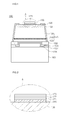
FIG. 1 is a cross-sectional view of a light emitting device according to an embodiment. -
FIG. 2 is an extended view of an A portion inFIG. 1 . -
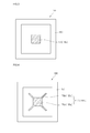
FIG. 3 is a plan view of the light emitting device according to the embodiment. -
FIG. 4 is a plan view of the light emitting device according to a modified example. -
FIG. 5 is a plan view of the light emitting device according to another modified example. -
FIG. 6 is a graph showing elementary analysis results of an interface between an electrode and a light emitting structe in a light emitting device according to Exemplary embodiment and Comprative embodiment. -
FIG. 7 is a graph showing an atomic concentration in the light emitting device according to Exemplary embodiment and Comprative embodiment. -
FIG. 8 is a voltage-current graph of the light emitting device according to Exemplary embodiment and Comprative embodiment. -
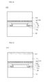
FIGs. 9 to 15 are cross-sectional views illustrating a method of manufacturing a light emitting device according to an embodiment. -
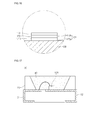
FIG. 16 is an extended view of an electrode according to still another modified example. -
FIG. 17 is a cross-sectional view of a light emitting device package including a light emitting device according to embodiments. -
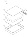
FIG. 18 is a disassembled perspective view of a backlight unit including a light emitting device or a light emitting device package according to an embodiment. -
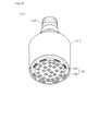
FIG. 19 is a perspective view of a lighting unit including a light emitting device or a light emitting device package according to an embodiment. - In the following description, it will be understood that when a layer (or film) is referred to as being "on" another layer or substrate, it can be directly on the other layer or substrate, or intervening layers may also be present. Further, it will be understood that when a layer is referred to as being "under" another layer, it can be directly under the other layer, and one or more intervening layers may also be present. In addition, it will also be understood that when a layer is referred to as being "between" two layers, it can be the only layer between the two layers, or one or more intervening layers may also be present. In addition, word "on," or "under," are will be described based on the accompanying drawings.
- In the figures, the dimensions of layers and regions are exaggerated for clarity of illustration. In addition, the dimension of each part does not reflect an actual size.
- Hereinafter, a light emitting device, a method of manufacturing the same, a light emitting device package, and a lighting system according to embodiments will be described with reference to the accompanying drawings.
-
FIG. 1 is a cross-sectional view of alight emitting device 100 according to an embodiment, andFIG. 2 is an extended view of an A portion inFIG. 1 .FIG. 3 is a plan view of thelight emitting device 100 according to the embodiment. - Referring to
FIGs. 1 and3 , thelight emitting device 100 according to the embodiment may include aconductive support member 160, anadhesive layer 158 on theconductive support member 160, areflective layer 157 on theadhesive layer 158, anohmic contact layer 156 on thereflective layer 157, aprotective layer 155 at a peripheral region on an upper surface of theadhesive layer 158, alight emitting structure 145 on theohmic contact layer 156 and theprotective layer 155, apassivation layer 163 on at least a side surface of thelight emitting structure 145, anelectrode 170 on an upper surface of thelight emitting structure 145, and anoxide layer 165 between theelectrode 170 and thelight emitting structure 145. Thelight emitting structure 145 may include an oxygen-injected region where oxygen is injected on its upper portion. - The
conductive support member 160 supports thelight emitting device 100, and provides a power to thelight emitting structure 145 together with theelectrode 170. - The
conductive support member 160 may include at least one selected from the group consisting of Ti, Cr, Ni, Al, Pt, Au, W, Cu, Mo and a carrier wafer, such as Si, Ge, GaAs, ZnO, SiC, SiGe, or GaN. - The
adhesive layer 158 may be formed on theconductive support member 160. Theadhesive layer 158 may be formed between thelight emitting structure 145 and theconductive support member 160 to bond them. Theadhesive layer 158 includes a barrier metal, a bonding metal, etc. For example, theadhesive layer 158 may include at least one of Ti, Au, Sn, Ni, Cr, In, Bi, Cu, Ag, and Ta. - The
reflective layer 157 may be formed on theadhesive layer 158. Thereflective layer 157 reflects light input from the lightemitting structure layer 145, thereby making it possible to improve the light extracting efficiency of thelight emitting device 100. Thereflective layer 157 may be made of metal having a high reflection efficiency. For example, thereflective layer 157 may include at least one of Ag, Ni, Al, Rh, Pd, Ir, Ru, Mg, Zn, Pt, Cu, Au, Hf or an alloy thereof. - The
ohmic contact layer 156 is formed on therelective layer 157. Theohmic contact layer 156 ohmic-contacts thelight emitting structure 145 to efficiently supply the power to thelight emitting structure 145. Theohmic contact layer 156 may selectively include a transparent conductive material or a metal. For example, theohmic contact layer 156 may be formed of a single layer or a multi-layer including at least one of ITO(indium tin oxide), IZO(indium zinc oxide), IZTO(indium zinc tin oxide), IAZO(indium aluminum zinc oxide), IGZO(indium gallium zinc oxide), IGTO(indium gallium tin oxide), AZO(aluminum zinc oxide), ATO(antimony tin oxide), GZO(gallium zinc oxide), IrOx, RuOx, RuOx/ITO, Ni, Ag, Ni/IrOx/Au, and Ni/IrOx/Au/ITO. - The
reflective layer 157 and theohmic contact layer 156 are not limited to the above. Thus, only one of thereflective layer 157 and theohmic contact layer 156 may be formed, or both of thereflective layer 157 and theohmic contact layer 156 may be omitted. - The
protective layer 155 may be formed at the peripheral region of the upper surface of theadhesive layer 158. In other words, theprotective layer 155 may be formed at the peripheral region between thelight emitting structure 145 and theadhesive layer 158. Theprotective layer 155 increases the distance from thelight emitting structure 145 to theadhesive layer 158 and theconductive support member 160, therby preventing the electrical short. - The
protective layer 155 may include transparent materials selected from oxides, nitrides, or insulating materials. For example, theprotective layer 155 may selectively include ITO(indium tin oxide), IZO(indium zinc oxide), IZTO(indium zinc tin oxide), IAZO(indium aluminum zinc oxide), IGZO(indium gallium zinc oxide), IGTO(indium gallium tin oxide), AZO(aluminum zinc oxide), ATO(antimony tin oxide), GZO(gallium zinc oxide), SiO2, SiOx, SiOxNy, Si3N4, Al2O3, ZrO2, Nb2O5, TiO2. - The
light emitting structure 145 may be formed on theohmic contact layer 156 and theprotective layer 155. - The
light emitting structure 145 is a structure generating a light and may include a plurality compound semiconductor layers. For example, the first conductivetype semiconductor layer 130, theactive layer 140 under the first conductivetype semiconductor layer 130, and the second conductivetype semiconductor layer 150 under theactive layer 140. For the convenience of the explanation, the second conductivetype semiconductor layer 150, theactive layer 140, and the first conductivetype semiconductor layer 130 will be described in sequence. - For example, the second conductive
type semiconductor layer 150 may includes a p type semiconductor layer. The p type semiconductor layer may include semiconductor materials having the compositional formula of InxAlyGa1-x-yN (0≤x≤1, 0≤y≤1, 0≤x+y≤1), such as InAlGaN, GaN, AlGaN, InGaN, AlInN, AIN, or InN. In addition, the p type semiconductor layer may be doped with p type dopant such as Mg, Zn, Ca, Sr, or Ba. - The
active layer 140 may formed on the second conductivetype semiconductor layer 150. Electrons (or holes) injected through the firstconductive semiconductor layer 130 may be recombined with holes (or electrons) injected through the secondconductive semiconductor layer 150 at theactive layer 140, so that theactive layer 140 emits the light based on the band gap difference of the energy band according to the intrinsic material of theactive layer 140. - The
active layer 140 may have a single quantum well structure, a multiple quantum well (MQW) structure, a quantum dot structure, or a quantum wire structure, but the embodiment is not limited thereto. - The
active layer 140 may include semiconductor materials having the compositional formula of InxAlyGa1-x-yN (0≤x≤1, 0≤y≤1, 0≤x+y≤1). In the case that theactive layer 140 has the multiple quantum well (MQW), theactive layer 140 may be formed of a plurality of well layers and a plurality of barrier layers. For example, theactive layer 140 has a plurality of pairs of an InGaN well layer/GaN barrier layer. - A clad layer (not shown) doped with the n type or p type dopant can be formed on and/or under the
active layer 140. The clad layer may include an AlGaN layer or an InAlGaN layer. - The first conductive
type semiconductor layer 130 may be formed on theactive layer 140. For instance, the firstconductive semiconductor layer 130 may include an n type semiconductor layer. The n type semiconductor layer may include semiconductor materials having the compositional formula of InxAlyGa1-x-yN (0≤x≤1, 0≤y≤1, 0≤x+y≤1), such as InAlGaN, GaN, ALGaN, AlInN, InGaN, AIN, or InN. In addition, the n type semiconductor layer may be doped with n type dopant such as Si, Ge, Sn, Se or Te. - Meanwhile, contrary to the above, the first conductive
type semiconductor layer 130 may include p type semiconductor layer, and the second conductivetype semiconductor layer 150 may include n type semiconductor layer. Also, a third conductive type semiconductor layer (not shown) including n type or p type semiconductor layer may be on the first conductivetype semiconductor layer 130. Accordingly, thelight emitting device 100 may include at least one of an N-P junction structure, a P-N junction structure, an N-P-N junction structure, and a P-N-P junction structure. In addition, the concentration of the dopant may be uniform or non-uniform in the first conductivetype semiconductor layer 130 and the second conductivetype semiconductor layer 150. That is, thelight emitting structure 145 can have various structures, and the embodiment is not limited thereto. - In the embodiment, the oxygen-injected
region 135 where oxygen is injected may be formed on the upper portion of the light emitting structure 145 (that is, the upper portion of the first conductive type semiconductor layer 130). For example, the oxygen-injectedregion 135 may be formed by an oxygen plasma treatment process, but is not limited thereto. - In the case that the first conductive
type semiconductor layer 130 includes galuim nitride(GaN), and the galuim(Ga) is outdiffused to an upper surface of the first conductivetype semiconductor layer 130 by forming the oxygen-injectedregion 135 on the first conductivetype semiconductor layer 130. - That is, the Ga contained in the first conductive
type semiconductor layer 130 is guided to move in the upper surface by the oxygen contained in the oxygen-injected region. Thus, the upper surface of the first conductivetype semiconductor layer 130 becomes a gallium-rich area. - In the case that the
electrode 170 is formed on the Ga-rich area, the contact resistance between theelectrode 170 and the Ga-rich area is reduced, compared with the case that the surface of the first conductive type semiconductor layer is a N-face that nitrogen (N2) is located at the upper surface. For example, the contact resistance may be in a range from about 1*10-3Ω·cm2 to about 5*10-3Ω·cm2 (about one-hundredth of the case that the surface of the first conductive type semiconductor layer is the N-face). Thus, according to the embodiment, the contact resistance between theelectrode 170 and the Ga-rich area can be greatly reduced by forming the oxygen-injectedregion 135. Thus, the light emitting efficiency of thelight emitting device 100 can be improved and the driving voltage of thelight emitting device 100 can decrease. - Also, between the
electrode 170 and thelight emitting structure 145, anoxide layer 165 may be formed by a combination of the oxygen contained in the oxygen-injectedregion 135 and the metal contained in a bottom surface of theelectrode 170. - Since the
oxide layer 165 is formed by the combination of the oxygen contained in the oxygen-injectedregion 135 and the metal contained in theelectrode 170, theoxide layer 165 has a thickness smaller than that of the oxygen-injectedregion 135 and that of theelectrode 170. Also, because theoxide layer 165 is formed by the combination of the oxygen contained in the oxygen-injectedregion 135 and the metal contained in theelectrode 170, theoxide layer 165 and theelectrode 170 have the same shape in a plan view, as shown inFIG. 3 , but is not limited thereto. InFIG. 3 , theoxide layer 165 and theelectrode 170 have rectangular shapes at a center region of thelight emitting structure 145. However, the embodiment is not limited thereto. Thus, as shown inFIG. 4 , theoxide layer 1165 and theelectrode 1170 may havefirst portions second portions first portions FIG. 5 , theoxide layer 2165 and theelectrode 2170 may include line portions having opening portions P. In this regard, the current can easily spread out. - Referring to
FIGs. 1 and 2 again, theoxide layer 165 may include a metal oxide. For example, theoxide layer 165 may include at least one of CrO, TiO2, Al2O3, AgO, and NiO. The material of theoxide layer 165 depends on the material of the bottom surface of theelectrode 170. - The
oxide layer 165 may have a thickness of about 0.1Å to about 100Å, and thus, the current can flows well by a tunneling effect therethrough. In addition, theoxide layer 165 is formed by the combination of the metal and the oxygen that easily reacts with each other. Thus, the generation of the material having a high insulating property (such as, CrN, GaO) can be prevented, thereby minimizing the increase of the contact resistance between theelectrode 170 and thelight emitting structure 145. - Hereinafter, a light emitting device according to an embodiment will be described in more detail with reference to
FIGs. 6 to 8 . - The elementary analysis results of an interface between an electrode and a light emitting structe in a light emitting device according to Exemplary embodiment and Comprative embodiment was shown in
FIG. 6 . The result was measured by AES(Auger Electron Spectroscopy). In Exemplary embodiment, oxygen was injected to alight emitting structure 145. In Comprative embodiment, oxygen was not injected to a light emitting structure. - Referring to
FIG. 6 , the width of oxygen peak generated between thelight emitting structure 145 and anelectrode 170 was broaden in the case (X) that an oxygen-injectedregion 135 was formed at thelight emitting structure 145 according to Exemplary embodiment, compared with the case (Y) that the oxygen-injected region was not formed at the light emitting structure according to Comparative embodiment. - The increases in the width of oxygen peak was because of the generation of the oxygen compound at an interface between the
electrode 170 and thelight emitting structure 145. Thus, it can be seen that theoxide layer 165 was formed. - The atomic concentration in the light emitting device according to Exemplary embodiment was shown in (a) of
FIG. 7 , and the atomic concentration in the light emitting device according to Comparative embodiment was shown in (b) ofFIG. 7 . - In more detail, the first conductive
type semiconductor layer 130 included GaN, theelectrode 170 included afirst layer 171 having Cr, asecond layer 172 having Ni, and athird layer 173 having Au. Exemplary embodiment and Comparative embodiment are only different from each other in that the oxygen was injected to alight emitting structure 145 in Examplary embodiment and the oxygen was not injected to the light emitting structure in Comparative embodiment. - Referring to (a) of
FIG. 7 , it can be seen that a portion C was formed between a portion A and a portion B. Here, the concentration of Ga and N were high in the portion A (that is, the light emitting structure portion), the concentration of Cr, Ni and Au were high in the portion B (that is, the electrode portion), and the concentration of Cr and O were high in the portion C (that is, the oxide layer portion). That is, it can be seen that theoxide layer 165 having CrO was formed between thelight emitting structure 145 and theelectrode 170 by the combination of the Cr contained in thefirst layer 171 and the oxygen. On the other hand, in (b) ofFIG. 7 , the oxide layer portion was not formed. - Last, a voltage-current of the light emitting device according to Exemplary embodiment and Comprative embodiment was measured by a TLM(transfer length method).
- Referring to
FIG. 8 , it can be seen that the contact resistance of the case (X) according to Examplary embodiment was smaller than that of the case (Y) according to Comparative embodiment. That is, according to Examplary embodiment, the contact resistance between thelight emitting structure 145 and theelectrode 170 can be reduced, and thus the light emitting efficiency can be improved. - Meanwhile, the Ga-rich area and a portion of the
oxide layer 165 may be overlapped with each other, and thus, it is possible that the Ga-rich area and the oxide layer are not clearly discriminated. In this case, theoxide layer 165 and the Ga-rich area may coexist between thelight emitting structure 145 and theelectrode 170 as shown in the above result. - Referring to
FIGs. 1 and 2 again, theelectrode 170 may be formed on theoxide layer 165. Theelectrode 170 may supply the power to thelight emitting device 100, together with theconductive support member 160. - As shown in
FIG. 2 , theelectrode 170 may have a plurality of layers. - In more detail, a
first layer 171 as the lowest layer includes a metal forming an ohmic contact with thelight emitting structure 145. For example, thefirst layer 171 may include at least one of Cr, Cr-Alloy, Al, Al-Alloy, Ti, Ti-Alloy, Ag, Ag-Alloy, Ni or Ni-Alloy. - A
third layer 173 as the highest layer includes a metal that the wire can be easily bonded. For example, thethird layer 173 may be formed in a single layer or multi-layer structure including at least one of Au, Al, Cu, or Cu-Alloy. - A
second layer 172 between thefirst layer 171 and thethird layer 173 may include a material that can prevent an inter-diffusion between thefirst layer 171 and thethird layer 173. For example, thesecond layer 172 may includes at least one of Ni, Ni-Alloy, Ti, or Ti-Alloy. However, the embodiment is not limited to the above structure of theelectrode 170. - The
passivation layer 163 may be formed on at least a side surface of thelight emitting structure 145. Thepassivation layer 163 may be formed to electrically insulate the side surface of thelight emitting structure 145 from an outer electrode (not shown), but is not limited thereto. - As shown, one end of the
passivation layer 163 may be formed on the upper surface of thelight emitting structure 145 and the other end of thepassivation layer 163 may be formed on theprotective layer 155. However, the present invention is not limited thereto. - For example, the
passivation layer 163 may include SiO2, SiOx, SiOxNy, Si3N4, or Al2O3 but is not limited thereto. - Hereinafter, a method for manufacturing a
light emitting device 100 according to the embodiment will be described in detail. -
FIGs. 9 to 15 are cross-sectional views illustrating a method of manufacturing alight emitting device 100 according to an embodiment. - Referring to
FIG. 9 , thelight emitting structure 145 may be formed on agrowth substrate 110. - The
growth substrate 110 may be made of at least one of, for example, sapphire (Al2O3), SiC, GaAs, GaN, ZnO, Si, GaP, InP, and Ge, but is not limited thereto. - The
light emitting structure 145 may be formed by growing the first conductivetype semiconductor layer 130, theactive layer 140, and the second conductivetype semiconductor layer 150 on thegrowth substrate 110. - The
light emitting structure 145 may be formed, for example, using a MOCVD (Metal Organic Chemical Vapor Deposition) method, a CVD (Chemical Vapor Deposition) method, a PECVD (Plasma-Enhanced Chemical Vapor Deposition) method, an MBE (Molecular Beam Epitaxy) method, an HVPE (Hydride Vapor Phase Epitaxy) method, etc., but is not limited thereto. - Meanwhile, a buffer layer (not shown) may be formed to relieve lattice mismatch due to a lattice constant difference between the
light emitting structure 145 and thegrowth substrate 110. - Referring to
FIG. 10 , theprotective layer 155 may be formed at a peripheral region on the upper surface of thelight emitting structure 145. - The
protective layer 155 may be formed, for example, using a PECVD (Plasma-Enhanced Chemical Vapor Deposition) method, an E-beam deposition method, etc., but is not limited thereto. - Referring to
FIG. 11 , theohmic contact layer 156, thereflective layer 157, theadhesive layer 158, and theconductive support member 160 may be sequentially formed on thelight emitting structure 145. - The
ohmic contact layer 156, thereflective layer 157, and theadhesive layer 158 may be formed by, for example, a PECVD (Plasma-Enhanced Chemical Vapor Deposition) method, a sputtering method, an E-beam method, a sputtering method, etc. In the case that theohmic contact layer 156, thereflective layer 157, or theadhesive layer 158 is formed of a metal, it may be formed by a plating method. - The
conductive support member 160 may be formed by the plating manner or the deposition manner. Altenativley, theconductive support member 160 of a separate sheet may be attached by the bonding manner. - Referring to
FIG. 12 , thegrowth substrate 110 may be removed from thelight emitting structure 145. - The
growth substrate 110 may be removed by a laser lift off method or an etching method but is not limited thereto.FIG. 12 shows the case where the structure shown inFIG. 11 is turned over, because the process removing thegrowth substrate 110 and the subsequent processes are performed at the bottom surface of thelight emitting structure 145 ofFIG. 11 . - Referring to
FIG. 10 , the light emittingstructure layer 145 is subject to the isolation etching along the unit chip region, such that the plurality oflight emitting structure 145 is separated. For example, the isolation etching may be performed by a dry etching method such as an inductively coupled plasma (ICP) method. - The upper surface of the first conductive
type semiconductor layer 130 of thelight emitting structure 145 is exposed by removing thegrowth substrate 110. - Referring to
FIG. 13 , the oxygen is injected to the exposed upper region of the first conductivetype semiconductor layer 130, thereby forming the oxygen-injectedregion 135. - The oxygen-injected
region 135 may be formed by, for example, an oxygen plasma treatment process. - That is, the Ga contained in the first conductive
type semiconductor layer 130 is guided to move toward its upper surface by forming the oxygen-injectedregion 135. Thus, the surface of the first conductivetype semiconductor layer 130 become a Ga-rich area. - As described above, the Ga-rich area achive the low contact resistance from about 1*10-3Ω·cm2 to about 5*10-3Ω·cm2. Thus, according to the embodiment, the driving voltage of the
light emitting device 100 can decrease and the light emitting efficiency of thelight emitting device 100 can be improved. - Referring to
FIG. 14 , theelectrode 170 may be formed on the first conductivetype semiconductor layer 130. - Then, the
oxide layer 165 with a thickness from 0.1 Å to 100 Å may be formed by a combination of the oxygen contained in the Ga-rich area at the first conductivetype semiconductor layer 130 and the metal contained in the bottom surface of theelectrode 170. - Thus, the
oxide layer 165 may include a metal oxide. For example, theoxide layer 165 may include at least one of CrO, TiO2, Al2O3, AgO or NiO. Since theoxide layer 165 is thin, the current can flows well between theelectrode 170 and thelight emitting structure 145 by a tunneling effect. Also, the generation of the material having a high insulating property (such as, CrN, GaO) can be prevented. - Referring to
FIG. 15 , thelight emitting structure 145 is subject to the isolation etching and thepassivatin 163 is formed on at least the side surface of thelight emitting structure 145. Then, thelight emitting device 100 according to the embodiment can be provided. - By the above isolation etching, a plurality of light emitting
devices 100 can be separated to unit devices. For example, the isolation etching may be performed by a dry etching method such as an inductively coupled plasma (ICP) method. - The
passivatin 163 may formed by deposition manners such as PECVD, sputtering, or E-beam deposition. - In the above embodiment, the
oxide layer 165 is formed between theelectrode 170 and thelight emitting structure 145, but is not limted thereto. Thus, shown inFIG. 16 , it is possible that the oxide layer 165 (inFIG. 1 ) is not separately formed. In this case, an oxygen concentration of afirst region 172a is higher than an oxygen concentration of asecond region 172b. Here, thefirst region 172a of theelectrode 172 is adjacent to the light emitting structure 145 (inFIG. 1 )(in more detail, the first conductive type semiconductor layer 130), and thesecond region 172b is formed on thefirst region 172a. Thefirst region 172a includes the metal contained in the lowest layer of theelectrode 172. For example, thefirst region 172a may include CrO, TiO2, Al2O3, AgO, or NiO. Here, thefirst region 172a may be thinner than the lowest layer of the electrode 172 (that is, the first layer 1711). The first, second, andthird layers -
FIG. 17 is a cross-sectional view of a light emitting device package including a light emitting device according to embodiments. - Referring to
FIG. 17 , the light emitting device package according to the embodiment includes apackage body 20, first and second electrode layers 31 and 32 mounted on thepackage body 20, alight emitting device 100 according to the embodiments, which is mounted on thepackage body 20 and electrically connected to the first and second electrode layers 31 and 32, and amolding member 40 enclosing thelight emitting device 100. - The
package body 20 may be formed including a silicon material, a synthetic resin material, or a metallic material, and may have an inclination surface around thelight emitting device 100. - The
first electrode layer 31 and thesecond electrode layer 32 are electrically separated, and supply an electric power to thelight emitting device 100. Also, the first and second electrode layers 31 and 32 may reflect light generated from thelight emitting device 100 to thus increase light efficiency, and may emit heat generated from thelight emitting device 100 to an outside. - The
light emitting device 100 may be mounted on thepackage body 20 or on thefirst electrode layer 31 or thesecond electrode layer 32. - The
light emitting device 100 may be electrically connected to thefirst electrode layer 31 and thesecond electrode layer 32 by using any one of a wire bonding method, a flip chip method, or a die bonding method. - The
molding member 40 may enclose and protect thelight emitting device 100. Also, a fluorescent material may be included in themolding member 40 to change the wavelength of light emitted from thelight emitting device 100. - The light emitting device package according to the current embodiment may mount at least one of the light emitting devices according to the foregoing embodiments, but the present invention is not limited thereto. The light emitting device package may include a plurality of light emitting device packages which are arrayed on a substrate. A plurality of optical members, such as a light guide panel, a prism sheet, a diffusion sheet, a fluorescent sheet, and the like may be arranged on a path of light emitted from the light emitting device package. The light emitting device package, substrate and optical members may function as a backlight unit or lighting unit, and a lighting system may include, for example, a backlight unit, a lighting unit, an indicator unit, a lamp, a streetlamp, etc.
-
FIG. 18 is a disassembled perspective view of a backlight unit including a light emitting device or a light emitting device package according to an embodiment. Thebacklight unit 1100 ofFIG. 18 is one example of lighting systems, and the present invention is not limited thereto. - Referring to
FIG. 18 , thebacklight unit 1100 may include abottom cover 1140, alight guide member 1120 disposed in thebottom cover 1140, and alight emitting module 1110 disposed on at least one side surface of thelight guide member 1120 or under thelight guide member 1120. Also, areflective sheet 1130 may be disposed under thelight guide member 1120. - The
bottom cover 1140 may be formed in a box shape a top surface of which is opened such that thelight guide member 1120, thelight emitting module 1110 and thereflective sheet 1130 can be received. Thebottom cover 1140 may be formed of a metal or resin material, but the invention is not limited thereto. - The
light emitting module 1110 may include asubstrate 700 and a plurality of light emitting device packages 600 mounted on thesubstrate 700. The plurality of light emitting device packages 600 may provide light to thelight guide member 1120. In thelight emitting module 1110 according to the current embodiment, it is exemplarily shown that the light emitting device packages 600 are mounted on thesubstrate 700, but the light emitting devices according to the embodiments may be mounted directly on thesubstrate 700. - As shown in
FIG. 18 , thelight emitting module 1110 may be disposed on at least one of inner side surfaces of thebottom cover 1140, and thus may provide light to at least one of the side surfaces of thelight guide member 1120. - It is also to be understood that the
light emitting module 1110 may be disposed under thelight guide member 1120 inside thebottom cover 1140 to provide light toward a bottom surface of thelight guide member 1120. However, since such a constitution may be modified according to the design of thebacklight unit 1100, the invention is not limited thereto. - The
light guide member 1120 may be disposed inside thebottom cover 1140. Thelight guide member 1120 may convert the light provided from the light emitting module to a planar light source and guide the converted plane light source to a display panel (not shown). - The
light guide member 1120 may be, for example, a light guide panel (LGP). The LGP may be formed of, for example, one of acryl-series resin such as polymethyl metaacrylate (PMMA), polyethylene terephthlate (PET), poly carbonate (PC), COC, and polyethylene naphthalate resin. - An
optical sheet 1150 may be disposed on thelight guide member 1120. - The
optical sheet 1150 may include, for example, at least one of a diffusion sheet, a light-condensing sheet, a brightness enhancement sheet and a fluorescent sheet. For example, theoptical sheet 1150 may be configured by the diffusion sheet, the light-condensing sheet, the brightness enhancement sheet and the fluorescent sheet stacked. In this case, thediffusion sheet 1150 diffuses the light emitted from thelight emitting module 1110 uniformly, and the diffused light may be condensed on the display panel (not shown) by the light-condensing sheet. At this time, the light emitted from the light-condensing sheet is a randomly polarized light, and the brightness enhancement sheet may increase the polarization of the light emitted from the light-condensing sheet. The light-condensing sheet may be, for example, a horizontal and/or vertical prism sheet. Also, the brightness enhancement sheet may be, for example, a dual brightness enhancement film. Also, the fluorescent sheet may be a transparent plate or film including a fluorescent material. - The
reflective sheet 1130 may be disposed under thelight guide member 1120. Thereflective sheet 1130 may reflect light emitted from the bottom surface of thelight guide member 1120 toward a light emitting surface of thelight guide member 1120. - The
reflective sheet 1130 may be formed of resin material having good reflectivity, for example, PET, PC, PVC resins, or the like, but the invention is not limited thereto. -
FIG. 19 is a perspective view of a lighting unit including a light emitting device or a light emitting device package according to an embodiment. Thelighting unit 1200 ofFIG. 19 is an example of lighting systems and the invention is not limited thereto. - Referring to
FIG. 19 , thelighting unit 1200 may include acase body 1210, alight emitting module 1230 installed in thecase body 1210, and a connection terminal installed in thecase body 1210 to be supplied with an electric power from an external power source. - The
case body 1210 may be preferably formed of a material having good heat shielding characteristic, for example, a metal material or a resin material. - The
light emitting module 1230 may include asubstrate 700, and a light emittingdevice package 600 mounted on thesubstrate 700. In thelight emitting module 1230 according to the current embodiment, it is exemplarily shown that the light emitting device packages 600 are mounted on thesubstrate 700, but the light emitting devices according to the embodiments may be mounted directly on thesubstrate 700. - The
substrate 700 may be an insulator substrate on which a circuit pattern is printed, and may include, for example, a general printed circuit board (PCB), a metal core PCB, a flexible PCB, a ceramic PCB, etc. - Also, the
substrate 700 may be formed of a material to efficiently reflect light, and a surface thereof may be formed in a color capable of efficiently reflecting light, for example, white color, silver color, or the like. - At least one light emitting
device package 600 may be mounted on thesubstrate 700. Each of the light emitting device packages 600 may include at least one light emitting diode (LED). The light emitting diode may include a color LED emitting red, green, blue or white light, and a UV LED emitting ultraviolet (UV). - The
light emitting module 1230 may have a combination of several LEDs so as to obtain desired color and luminance. For example, thelight emitting module 1230 may have a combination of a white LED, a red LED, and a green LED so as to obtain a high color rendering index (CRI). A fluorescent sheet may be further disposed on a path of light emitted from thelight emitting module 1230. The fluorescent sheet converts the wavelength of the light emitted from the light emitting module. For example, when the light emitted from thelight emitting module 1230 has a blue wavelength band, the fluorescent sheet may include a yellow fluorescent material, so that the light, which is emitted from thelight emitting module 1230 and passes through the fluorescent sheet, finally appears as white light. - The
connection terminal 1220 may be electrically connected to thelight emitting module 1230 to supply an electric power to thelight emitting module 1230. As shown inFIG. 19 , theconnection terminal 1220 may be screwed and coupled to an external power, but the invention is not limited thereto. For example, theconnection terminal 1220 may be made in a pin type and inserted into an external power, or may be connected to the external power through a power line. - As described above, the lighting system may include at least one of a light guide member, a diffusion sheet, a light-condensing sheet, a brightness enhancement sheet and a fluorescent sheet on a traveling path of light to obtain a desired optical effect.
- As described above, since the lighting system according to this embodiment includes the light emitting device or light emitting device package capable of emitting light having a high light emitting efficiency, the lighting system can show superior characteristics.
- Any reference in this specification to "one embodiment," "an embodiment," "example embodiment," etc., means that a particular feature, structure, or characteristic described in connection with the embodiment is included in at least one embodiment of the invention. The appearances of such phrases in various places in the specification are not necessarily all referring to the same embodiment. Further, when a particular feature, structure, or characteristic is described in connection with any embodiment, it is submitted that it is within the purview of one skilled in the art to effect such feature, structure, or characteristic in connection with other ones of the embodiments.
- Although embodiments have been described with reference to a number of illustrative embodiments thereof, it should be understood that numerous other modifications and embodiments can be devised by those skilled in the art that will fall within the spirit and scope of the principles of this disclosure. More particularly, various variations and modifications are possible in the component parts and/or arrangements of the subject combination arrangement within the scope of the disclosure, the drawings and the appended claims. In addition to variations and modifications in the component parts and/or arrangements, alternative uses will also be apparent to those skilled in the art.
Claims (15)
- A light emitting device comprising:a conductive support member;a light emitting structure on the conductive support member, the light emitting structure comprising a first conductive type semiconductor layer, a second conductive type semiconductor layer, and an active layer between the first conductive type semiconductor layer and the second conductive type semiconductor layer; andan electrode on the light emitting structure,wherein the light emitting structure comprises an oxygen-injected region where oxygen is injected on an upper portion of the light emitting structure, andwherein the electrode comprises a first region and a second region on the first region, and an oxygen concentration of the first region is higher than an oxygen concentration of the second region.
- The light emitting device of claim 1, wherein the first region forms an oxide layer.
- The light emitting device of claim 2, wherein the upper portion of the light emitting structure includes galuim nitride(GaN), and the galuim is outdiffused to an upper surface of the light emitting structure by the oxygen in the oxygen-injected region.
- The light emitting device of claim 1, wherein the oxygen-injected region includes a gallium-rich area.
- The light emitting device of claim 1, wherein the first region includes a metal oxide.
- The light emitting device of claim 1, wherein the first region comprises at least one selected from the group consisting of CrO, TiO2, Al2O3, AgO or NiO.
- The light emitting device of claim 1, the electrode comprises a plurality of layers.
- The light emitting device of claim 7, wherein the first region includes a metal included in a first layer of the electode where is adjacent to the light emitting structure.
- The light emitting device of claim 8, wherein the first layer of the electrode comprises a metal forming an ohmic contact with the light emitting structure.
- The light emitting device of claim 8, wherein the first layer of the electrode comprises at least one selected from the group consisting of Cr, Cr-Alloy, Al, Al-Alloy, Ti, Ti-Alloy, Ag, Ag-Alloy, Ni and Ni-Alloy.
- The light emitting device of claim 2, wherein a thickness of the oxide layer is smaller than a thickness of the electrode.
- The light emitting device of claim 2, wherein a thickness of the oxide layer is smaller than a thickness of the light emitting structure.
- The light emitting device of claim 2, wherein a thickness of the oxide layer is in a range from about 0.1Å to about 100Å.
- The light emitting device of claim 2, wherein the oxide layer and the electrode have the same shape in a plan view.
- The light emitting device of claim 1, wherein the contact resistance between the light emitting structure and the electrode is in a range from about 1*10-3Ω·cm2 to about 5*10-3Ω·cm2.
Applications Claiming Priority (1)
| Application Number | Priority Date | Filing Date | Title |
|---|---|---|---|
| KR1020100012318A KR100999747B1 (en) | 2010-02-10 | 2010-02-10 | Light emitting device, light emitting device manufacturing method and light emitting device package |
Publications (2)
| Publication Number | Publication Date |
|---|---|
| EP2355186A1 true EP2355186A1 (en) | 2011-08-10 |
| EP2355186B1 EP2355186B1 (en) | 2017-12-27 |
Family
ID=43512605
Family Applications (1)
| Application Number | Title | Priority Date | Filing Date |
|---|---|---|---|
| EP11152177.9A Active EP2355186B1 (en) | 2010-02-10 | 2011-01-26 | Light emitting device comprising an oxygen-injected region |
Country Status (6)
| Country | Link |
|---|---|
| US (1) | US8455880B2 (en) |
| EP (1) | EP2355186B1 (en) |
| JP (1) | JP5513424B2 (en) |
| KR (1) | KR100999747B1 (en) |
| CN (1) | CN102148307B (en) |
| TW (1) | TWI437734B (en) |
Cited By (1)
| Publication number | Priority date | Publication date | Assignee | Title |
|---|---|---|---|---|
| EP2423986A3 (en) * | 2010-08-30 | 2014-11-12 | LG Innotek Co., Ltd. | Light emitting device |
Families Citing this family (10)
| Publication number | Priority date | Publication date | Assignee | Title |
|---|---|---|---|---|
| KR101020945B1 (en) * | 2009-12-21 | 2011-03-09 | 엘지이노텍 주식회사 | Light emitting device, light emitting device package and manufacturing method |
| JP5899734B2 (en) * | 2011-09-16 | 2016-04-06 | 日亜化学工業株式会社 | Light emitting device |
| US20140091330A1 (en) * | 2012-10-02 | 2014-04-03 | Helio Optoelectronics Corporation | Led package structure with transparent electrodes |
| CN103413875B (en) * | 2013-09-09 | 2016-05-11 | 聚灿光电科技股份有限公司 | A kind of preparation method of PN step of PN step, LED chip and LED chip of LED chip |
| CN104795316A (en) * | 2015-04-17 | 2015-07-22 | 上海华虹宏力半导体制造有限公司 | Manufacturing method of integrated resistor |
| CN105511149B (en) * | 2016-01-28 | 2020-03-31 | 京东方科技集团股份有限公司 | Display panel and display device |
| TWI605682B (en) * | 2016-08-12 | 2017-11-11 | 郭哲豪 | Quantum? dots-containing? flexible? luminescent solar concentrators? and the preparation method thereof |
| DE102017002332B4 (en) * | 2017-03-13 | 2019-11-07 | Azur Space Solar Power Gmbh | led |
| JP7612691B2 (en) * | 2019-12-11 | 2025-01-14 | 三星電子株式会社 | Light emitting diode die transfer method using partial laser lift-off - Patents.com |
| US11626532B2 (en) | 2021-01-06 | 2023-04-11 | Applied Materials, Inc. | Methods and apparatus for forming light emitting diodes |
Citations (6)
| Publication number | Priority date | Publication date | Assignee | Title |
|---|---|---|---|---|
| US4608581A (en) * | 1982-02-02 | 1986-08-26 | Bagratishvili Givi D | Semiconductor light emitter based on gallium nitride and process for manufacture thereof |
| US6057564A (en) * | 1997-07-30 | 2000-05-02 | Kabushiki Kaisha Toshiba | Semiconductor device having a GaNO region intermediate a GaN-based contact region and an electrode |
| US6329716B1 (en) * | 1997-01-14 | 2001-12-11 | Nec Corporation | Contact electrode for N-type gallium nitride-based compound semiconductor and method for forming the same |
| EP1655786A2 (en) * | 2004-11-08 | 2006-05-10 | Samsung Electro-mechanics Co., Ltd | Method of forming electrode for compound semiconductor device |
| US20060186417A1 (en) * | 2005-02-05 | 2006-08-24 | United Epitaxy Company, Ltd. | Light emitting diode and method making the same |
| US20090142871A1 (en) * | 2007-11-29 | 2009-06-04 | Mitsubishi Electric Corporation | Method of manufacturing semiconductor device |
Family Cites Families (9)
| Publication number | Priority date | Publication date | Assignee | Title |
|---|---|---|---|---|
| US4608305A (en) * | 1984-06-18 | 1986-08-26 | Texon, Inc. | Binder and shoeboard products containing three heat reactive resins |
| JP2002353144A (en) | 2001-05-23 | 2002-12-06 | Ricoh Co Ltd | P-type group III nitride semiconductor, method for manufacturing the same, and semiconductor device |
| JP2005136156A (en) | 2003-10-30 | 2005-05-26 | Shin Etsu Handotai Co Ltd | ZnO-BASED SEMICONDUCTOR LIGHT EMITTING DEVICE AND ITS MANUFACTURING METHOD |
| JP4536568B2 (en) * | 2005-03-31 | 2010-09-01 | 住友電工デバイス・イノベーション株式会社 | Method for manufacturing FET |
| JP4225510B2 (en) | 2005-07-06 | 2009-02-18 | 昭和電工株式会社 | Compound semiconductor light emitting diode and method for manufacturing the same |
| JP2007235000A (en) * | 2006-03-03 | 2007-09-13 | Eudyna Devices Inc | Semiconductor processing method, semiconductor device and manufacturing method thereof |
| EP1863324A1 (en) * | 2006-06-02 | 2007-12-05 | Semiconductor Energy Laboratory Co., Ltd. | Light emitting element and light emitting device |
| KR100874653B1 (en) | 2007-07-30 | 2008-12-17 | 고려대학교 산학협력단 | Nitride light emitting device and its manufacturing method |
| JP2010225767A (en) | 2009-03-23 | 2010-10-07 | Panasonic Corp | Nitride semiconductor light emitting device and manufacturing method thereof |
-
2010
- 2010-02-10 KR KR1020100012318A patent/KR100999747B1/en not_active Expired - Fee Related
-
2011
- 2011-01-21 TW TW100102274A patent/TWI437734B/en not_active IP Right Cessation
- 2011-01-26 EP EP11152177.9A patent/EP2355186B1/en active Active
- 2011-02-08 US US13/023,100 patent/US8455880B2/en active Active
- 2011-02-10 JP JP2011026733A patent/JP5513424B2/en active Active
- 2011-02-10 CN CN201110036993.4A patent/CN102148307B/en active Active
Patent Citations (6)
| Publication number | Priority date | Publication date | Assignee | Title |
|---|---|---|---|---|
| US4608581A (en) * | 1982-02-02 | 1986-08-26 | Bagratishvili Givi D | Semiconductor light emitter based on gallium nitride and process for manufacture thereof |
| US6329716B1 (en) * | 1997-01-14 | 2001-12-11 | Nec Corporation | Contact electrode for N-type gallium nitride-based compound semiconductor and method for forming the same |
| US6057564A (en) * | 1997-07-30 | 2000-05-02 | Kabushiki Kaisha Toshiba | Semiconductor device having a GaNO region intermediate a GaN-based contact region and an electrode |
| EP1655786A2 (en) * | 2004-11-08 | 2006-05-10 | Samsung Electro-mechanics Co., Ltd | Method of forming electrode for compound semiconductor device |
| US20060186417A1 (en) * | 2005-02-05 | 2006-08-24 | United Epitaxy Company, Ltd. | Light emitting diode and method making the same |
| US20090142871A1 (en) * | 2007-11-29 | 2009-06-04 | Mitsubishi Electric Corporation | Method of manufacturing semiconductor device |
Non-Patent Citations (1)
| Title |
|---|
| SONG JUNE O ET AL: "Highly low resistance and transparent Ni/ZnO ohmic contacts to p-type GaN", APPLIED PHYSICS LETTERS, AIP, AMERICAN INSTITUTE OF PHYSICS, MELVILLE, NY, US, vol. 83, no. 3, 21 July 2003 (2003-07-21), pages 479 - 481, XP012035519, ISSN: 0003-6951, DOI: 10.1063/1.1591236 * |
Cited By (1)
| Publication number | Priority date | Publication date | Assignee | Title |
|---|---|---|---|---|
| EP2423986A3 (en) * | 2010-08-30 | 2014-11-12 | LG Innotek Co., Ltd. | Light emitting device |
Also Published As
| Publication number | Publication date |
|---|---|
| TWI437734B (en) | 2014-05-11 |
| EP2355186B1 (en) | 2017-12-27 |
| CN102148307A (en) | 2011-08-10 |
| CN102148307B (en) | 2014-05-07 |
| JP5513424B2 (en) | 2014-06-04 |
| JP2011166149A (en) | 2011-08-25 |
| US8455880B2 (en) | 2013-06-04 |
| TW201131816A (en) | 2011-09-16 |
| KR100999747B1 (en) | 2010-12-08 |
| US20110193093A1 (en) | 2011-08-11 |
Similar Documents
| Publication | Publication Date | Title |
|---|---|---|
| EP2355186B1 (en) | Light emitting device comprising an oxygen-injected region | |
| US8723213B2 (en) | Light emitting device and light emitting device package | |
| EP2432036B1 (en) | Light emitting diode | |
| US9899581B2 (en) | Light emitting apparatus | |
| US8450762B2 (en) | Light emitting device | |
| EP2362447B1 (en) | Light emitting diode | |
| US9537056B2 (en) | Light emitting device | |
| US8803174B2 (en) | Light emitting device, light emitting device package | |
| US8872215B2 (en) | Light emitting device and light emitting device package | |
| US8390014B2 (en) | Light emitting device and light emitting device package | |
| US8525215B2 (en) | Light emitting device, method of manufacturing the same, light emitting device package, and lighting system | |
| KR101990095B1 (en) | Light emitting device, method for fabricating the same, and light emitting device package | |
| EP2372792B1 (en) | Light emitting device, method for fabricating light emittng device, and light emitting device package | |
| KR102075151B1 (en) | Light emitting device, light emitting device package, and light unit | |
| KR20120022091A (en) | Light emitting device, method for fabricating the light emitting device, light emitting device package and lighting system | |
| KR20120042516A (en) | Light emitting device, method for fabricating the light emitting device, light emitting device package and lighting system | |
| KR20120045635A (en) | Light emitting device, method for fabricating the light emitting device, light emitting device package and lighting system | |
| KR20120029868A (en) | Light emitting device, light emitting device package and lighting system | |
| KR20120038337A (en) | Light emitting device, method for fabricating the light emitting device, light emitting device package and lighting system |
Legal Events
| Date | Code | Title | Description |
|---|---|---|---|
| PUAI | Public reference made under article 153(3) epc to a published international application that has entered the european phase |
Free format text: ORIGINAL CODE: 0009012 |
|
| 17P | Request for examination filed |
Effective date: 20110126 |
|
| AK | Designated contracting states |
Kind code of ref document: A1 Designated state(s): AL AT BE BG CH CY CZ DE DK EE ES FI FR GB GR HR HU IE IS IT LI LT LU LV MC MK MT NL NO PL PT RO RS SE SI SK SM TR |
|
| AX | Request for extension of the european patent |
Extension state: BA ME |
|
| RAP1 | Party data changed (applicant data changed or rights of an application transferred) |
Owner name: LG INNOTEK CO., LTD. |
|
| 17Q | First examination report despatched |
Effective date: 20160322 |
|
| STAA | Information on the status of an ep patent application or granted ep patent |
Free format text: STATUS: EXAMINATION IS IN PROGRESS |
|
| RAP1 | Party data changed (applicant data changed or rights of an application transferred) |
Owner name: LG INNOTEK CO., LTD. |
|
| RIC1 | Information provided on ipc code assigned before grant |
Ipc: H01L 33/40 20100101AFI20170524BHEP Ipc: H01L 33/02 20100101ALI20170524BHEP Ipc: H01L 33/32 20100101ALN20170524BHEP |
|
| GRAP | Despatch of communication of intention to grant a patent |
Free format text: ORIGINAL CODE: EPIDOSNIGR1 |
|
| STAA | Information on the status of an ep patent application or granted ep patent |
Free format text: STATUS: GRANT OF PATENT IS INTENDED |
|
| RIC1 | Information provided on ipc code assigned before grant |
Ipc: H01L 33/02 20100101ALI20170601BHEP Ipc: H01L 33/40 20100101AFI20170601BHEP Ipc: H01L 33/32 20100101ALN20170601BHEP |
|
| INTG | Intention to grant announced |
Effective date: 20170703 |
|
| GRAS | Grant fee paid |
Free format text: ORIGINAL CODE: EPIDOSNIGR3 |
|
| GRAA | (expected) grant |
Free format text: ORIGINAL CODE: 0009210 |
|
| STAA | Information on the status of an ep patent application or granted ep patent |
Free format text: STATUS: THE PATENT HAS BEEN GRANTED |
|
| AK | Designated contracting states |
Kind code of ref document: B1 Designated state(s): AL AT BE BG CH CY CZ DE DK EE ES FI FR GB GR HR HU IE IS IT LI LT LU LV MC MK MT NL NO PL PT RO RS SE SI SK SM TR |
|
| REG | Reference to a national code |
Ref country code: GB Ref legal event code: FG4D |
|
| REG | Reference to a national code |
Ref country code: CH Ref legal event code: EP |
|
| REG | Reference to a national code |
Ref country code: AT Ref legal event code: REF Ref document number: 959004 Country of ref document: AT Kind code of ref document: T Effective date: 20180115 |
|
| REG | Reference to a national code |
Ref country code: IE Ref legal event code: FG4D |
|
| REG | Reference to a national code |
Ref country code: DE Ref legal event code: R096 Ref document number: 602011044497 Country of ref document: DE |
|
| PG25 | Lapsed in a contracting state [announced via postgrant information from national office to epo] |
Ref country code: FI Free format text: LAPSE BECAUSE OF FAILURE TO SUBMIT A TRANSLATION OF THE DESCRIPTION OR TO PAY THE FEE WITHIN THE PRESCRIBED TIME-LIMIT Effective date: 20171227 Ref country code: NO Free format text: LAPSE BECAUSE OF FAILURE TO SUBMIT A TRANSLATION OF THE DESCRIPTION OR TO PAY THE FEE WITHIN THE PRESCRIBED TIME-LIMIT Effective date: 20180327 Ref country code: LT Free format text: LAPSE BECAUSE OF FAILURE TO SUBMIT A TRANSLATION OF THE DESCRIPTION OR TO PAY THE FEE WITHIN THE PRESCRIBED TIME-LIMIT Effective date: 20171227 |
|
| REG | Reference to a national code |
Ref country code: NL Ref legal event code: MP Effective date: 20171227 |
|
| REG | Reference to a national code |
Ref country code: LT Ref legal event code: MG4D |
|
| REG | Reference to a national code |
Ref country code: AT Ref legal event code: MK05 Ref document number: 959004 Country of ref document: AT Kind code of ref document: T Effective date: 20171227 |
|
| PG25 | Lapsed in a contracting state [announced via postgrant information from national office to epo] |
Ref country code: LV Free format text: LAPSE BECAUSE OF FAILURE TO SUBMIT A TRANSLATION OF THE DESCRIPTION OR TO PAY THE FEE WITHIN THE PRESCRIBED TIME-LIMIT Effective date: 20171227 Ref country code: GR Free format text: LAPSE BECAUSE OF FAILURE TO SUBMIT A TRANSLATION OF THE DESCRIPTION OR TO PAY THE FEE WITHIN THE PRESCRIBED TIME-LIMIT Effective date: 20180328 Ref country code: HR Free format text: LAPSE BECAUSE OF FAILURE TO SUBMIT A TRANSLATION OF THE DESCRIPTION OR TO PAY THE FEE WITHIN THE PRESCRIBED TIME-LIMIT Effective date: 20171227 Ref country code: BG Free format text: LAPSE BECAUSE OF FAILURE TO SUBMIT A TRANSLATION OF THE DESCRIPTION OR TO PAY THE FEE WITHIN THE PRESCRIBED TIME-LIMIT Effective date: 20180327 Ref country code: RS Free format text: LAPSE BECAUSE OF FAILURE TO SUBMIT A TRANSLATION OF THE DESCRIPTION OR TO PAY THE FEE WITHIN THE PRESCRIBED TIME-LIMIT Effective date: 20171227 |
|
| PG25 | Lapsed in a contracting state [announced via postgrant information from national office to epo] |
Ref country code: NL Free format text: LAPSE BECAUSE OF FAILURE TO SUBMIT A TRANSLATION OF THE DESCRIPTION OR TO PAY THE FEE WITHIN THE PRESCRIBED TIME-LIMIT Effective date: 20171227 |
|
| PG25 | Lapsed in a contracting state [announced via postgrant information from national office to epo] |
Ref country code: ES Free format text: LAPSE BECAUSE OF FAILURE TO SUBMIT A TRANSLATION OF THE DESCRIPTION OR TO PAY THE FEE WITHIN THE PRESCRIBED TIME-LIMIT Effective date: 20171227 Ref country code: EE Free format text: LAPSE BECAUSE OF FAILURE TO SUBMIT A TRANSLATION OF THE DESCRIPTION OR TO PAY THE FEE WITHIN THE PRESCRIBED TIME-LIMIT Effective date: 20171227 Ref country code: CY Free format text: LAPSE BECAUSE OF FAILURE TO SUBMIT A TRANSLATION OF THE DESCRIPTION OR TO PAY THE FEE WITHIN THE PRESCRIBED TIME-LIMIT Effective date: 20171227 Ref country code: SK Free format text: LAPSE BECAUSE OF FAILURE TO SUBMIT A TRANSLATION OF THE DESCRIPTION OR TO PAY THE FEE WITHIN THE PRESCRIBED TIME-LIMIT Effective date: 20171227 Ref country code: CZ Free format text: LAPSE BECAUSE OF FAILURE TO SUBMIT A TRANSLATION OF THE DESCRIPTION OR TO PAY THE FEE WITHIN THE PRESCRIBED TIME-LIMIT Effective date: 20171227 |
|
| PG25 | Lapsed in a contracting state [announced via postgrant information from national office to epo] |
Ref country code: AT Free format text: LAPSE BECAUSE OF FAILURE TO SUBMIT A TRANSLATION OF THE DESCRIPTION OR TO PAY THE FEE WITHIN THE PRESCRIBED TIME-LIMIT Effective date: 20171227 Ref country code: IT Free format text: LAPSE BECAUSE OF FAILURE TO SUBMIT A TRANSLATION OF THE DESCRIPTION OR TO PAY THE FEE WITHIN THE PRESCRIBED TIME-LIMIT Effective date: 20171227 Ref country code: SM Free format text: LAPSE BECAUSE OF FAILURE TO SUBMIT A TRANSLATION OF THE DESCRIPTION OR TO PAY THE FEE WITHIN THE PRESCRIBED TIME-LIMIT Effective date: 20171227 Ref country code: RO Free format text: LAPSE BECAUSE OF FAILURE TO SUBMIT A TRANSLATION OF THE DESCRIPTION OR TO PAY THE FEE WITHIN THE PRESCRIBED TIME-LIMIT Effective date: 20171227 Ref country code: IS Free format text: LAPSE BECAUSE OF FAILURE TO SUBMIT A TRANSLATION OF THE DESCRIPTION OR TO PAY THE FEE WITHIN THE PRESCRIBED TIME-LIMIT Effective date: 20180427 Ref country code: PL Free format text: LAPSE BECAUSE OF FAILURE TO SUBMIT A TRANSLATION OF THE DESCRIPTION OR TO PAY THE FEE WITHIN THE PRESCRIBED TIME-LIMIT Effective date: 20171227 |
|
| REG | Reference to a national code |
Ref country code: CH Ref legal event code: PL |
|
| PG25 | Lapsed in a contracting state [announced via postgrant information from national office to epo] |
Ref country code: MC Free format text: LAPSE BECAUSE OF FAILURE TO SUBMIT A TRANSLATION OF THE DESCRIPTION OR TO PAY THE FEE WITHIN THE PRESCRIBED TIME-LIMIT Effective date: 20171227 |
|
| REG | Reference to a national code |
Ref country code: DE Ref legal event code: R097 Ref document number: 602011044497 Country of ref document: DE |
|
| PG25 | Lapsed in a contracting state [announced via postgrant information from national office to epo] |
Ref country code: FR Free format text: LAPSE BECAUSE OF NON-PAYMENT OF DUE FEES Effective date: 20180227 Ref country code: LU Free format text: LAPSE BECAUSE OF NON-PAYMENT OF DUE FEES Effective date: 20180126 |
|
| REG | Reference to a national code |
Ref country code: IE Ref legal event code: MM4A |
|
| PLBE | No opposition filed within time limit |
Free format text: ORIGINAL CODE: 0009261 |
|
| REG | Reference to a national code |
Ref country code: FR Ref legal event code: ST Effective date: 20180928 |
|
| STAA | Information on the status of an ep patent application or granted ep patent |
Free format text: STATUS: NO OPPOSITION FILED WITHIN TIME LIMIT |
|
| REG | Reference to a national code |
Ref country code: BE Ref legal event code: MM Effective date: 20180131 |
|
| GBPC | Gb: european patent ceased through non-payment of renewal fee |
Effective date: 20180327 |
|
| PG25 | Lapsed in a contracting state [announced via postgrant information from national office to epo] |
Ref country code: DK Free format text: LAPSE BECAUSE OF FAILURE TO SUBMIT A TRANSLATION OF THE DESCRIPTION OR TO PAY THE FEE WITHIN THE PRESCRIBED TIME-LIMIT Effective date: 20171227 Ref country code: BE Free format text: LAPSE BECAUSE OF NON-PAYMENT OF DUE FEES Effective date: 20180131 Ref country code: LI Free format text: LAPSE BECAUSE OF NON-PAYMENT OF DUE FEES Effective date: 20180131 Ref country code: CH Free format text: LAPSE BECAUSE OF NON-PAYMENT OF DUE FEES Effective date: 20180131 |
|
| 26N | No opposition filed |
Effective date: 20180928 |
|
| PG25 | Lapsed in a contracting state [announced via postgrant information from national office to epo] |
Ref country code: IE Free format text: LAPSE BECAUSE OF NON-PAYMENT OF DUE FEES Effective date: 20180126 |
|
| PG25 | Lapsed in a contracting state [announced via postgrant information from national office to epo] |
Ref country code: SI Free format text: LAPSE BECAUSE OF FAILURE TO SUBMIT A TRANSLATION OF THE DESCRIPTION OR TO PAY THE FEE WITHIN THE PRESCRIBED TIME-LIMIT Effective date: 20171227 Ref country code: GB Free format text: LAPSE BECAUSE OF NON-PAYMENT OF DUE FEES Effective date: 20180327 |
|
| PG25 | Lapsed in a contracting state [announced via postgrant information from national office to epo] |
Ref country code: MT Free format text: LAPSE BECAUSE OF NON-PAYMENT OF DUE FEES Effective date: 20180126 |
|
| PG25 | Lapsed in a contracting state [announced via postgrant information from national office to epo] |
Ref country code: TR Free format text: LAPSE BECAUSE OF FAILURE TO SUBMIT A TRANSLATION OF THE DESCRIPTION OR TO PAY THE FEE WITHIN THE PRESCRIBED TIME-LIMIT Effective date: 20171227 |
|
| PG25 | Lapsed in a contracting state [announced via postgrant information from national office to epo] |
Ref country code: HU Free format text: LAPSE BECAUSE OF FAILURE TO SUBMIT A TRANSLATION OF THE DESCRIPTION OR TO PAY THE FEE WITHIN THE PRESCRIBED TIME-LIMIT; INVALID AB INITIO Effective date: 20110126 Ref country code: PT Free format text: LAPSE BECAUSE OF FAILURE TO SUBMIT A TRANSLATION OF THE DESCRIPTION OR TO PAY THE FEE WITHIN THE PRESCRIBED TIME-LIMIT Effective date: 20171227 |
|
| PG25 | Lapsed in a contracting state [announced via postgrant information from national office to epo] |
Ref country code: MK Free format text: LAPSE BECAUSE OF NON-PAYMENT OF DUE FEES Effective date: 20171227 Ref country code: SE Free format text: LAPSE BECAUSE OF FAILURE TO SUBMIT A TRANSLATION OF THE DESCRIPTION OR TO PAY THE FEE WITHIN THE PRESCRIBED TIME-LIMIT Effective date: 20171227 |
|
| PG25 | Lapsed in a contracting state [announced via postgrant information from national office to epo] |
Ref country code: AL Free format text: LAPSE BECAUSE OF FAILURE TO SUBMIT A TRANSLATION OF THE DESCRIPTION OR TO PAY THE FEE WITHIN THE PRESCRIBED TIME-LIMIT Effective date: 20171227 |
|
| REG | Reference to a national code |
Ref country code: DE Ref legal event code: R081 Ref document number: 602011044497 Country of ref document: DE Owner name: SUZHOU LEKIN SEMICONDUCTOR CO. LTD., TAICANG, CN Free format text: FORMER OWNER: LG INNOTEK CO., LTD., SEOUL, KR |
|
| REG | Reference to a national code |
Ref country code: DE Ref legal event code: R079 Ref document number: 602011044497 Country of ref document: DE Free format text: PREVIOUS MAIN CLASS: H01L0033400000 Ipc: H10H0020832000 |
|
| PGFP | Annual fee paid to national office [announced via postgrant information from national office to epo] |
Ref country code: DE Payment date: 20251203 Year of fee payment: 16 |