EP2355139A1 - Thin film transistor manufacturing method, thin film transistor, and electronic device - Google Patents
Thin film transistor manufacturing method, thin film transistor, and electronic device Download PDFInfo
- Publication number
- EP2355139A1 EP2355139A1 EP09829071A EP09829071A EP2355139A1 EP 2355139 A1 EP2355139 A1 EP 2355139A1 EP 09829071 A EP09829071 A EP 09829071A EP 09829071 A EP09829071 A EP 09829071A EP 2355139 A1 EP2355139 A1 EP 2355139A1
- Authority
- EP
- European Patent Office
- Prior art keywords
- organic semiconductor
- pattern
- electrode
- thin film
- semiconductor pattern
- Prior art date
- Legal status (The legal status is an assumption and is not a legal conclusion. Google has not performed a legal analysis and makes no representation as to the accuracy of the status listed.)
- Granted
Links
Images






Classifications
-
- H—ELECTRICITY
- H10—SEMICONDUCTOR DEVICES; ELECTRIC SOLID-STATE DEVICES NOT OTHERWISE PROVIDED FOR
- H10K—ORGANIC ELECTRIC SOLID-STATE DEVICES
- H10K71/00—Manufacture or treatment specially adapted for the organic devices covered by this subclass
- H10K71/10—Deposition of organic active material
- H10K71/16—Deposition of organic active material using physical vapour deposition [PVD], e.g. vacuum deposition or sputtering
- H10K71/166—Deposition of organic active material using physical vapour deposition [PVD], e.g. vacuum deposition or sputtering using selective deposition, e.g. using a mask
-
- B—PERFORMING OPERATIONS; TRANSPORTING
- B82—NANOTECHNOLOGY
- B82Y—SPECIFIC USES OR APPLICATIONS OF NANOSTRUCTURES; MEASUREMENT OR ANALYSIS OF NANOSTRUCTURES; MANUFACTURE OR TREATMENT OF NANOSTRUCTURES
- B82Y10/00—Nanotechnology for information processing, storage or transmission, e.g. quantum computing or single electron logic
-
- H—ELECTRICITY
- H10—SEMICONDUCTOR DEVICES; ELECTRIC SOLID-STATE DEVICES NOT OTHERWISE PROVIDED FOR
- H10K—ORGANIC ELECTRIC SOLID-STATE DEVICES
- H10K10/00—Organic devices specially adapted for rectifying, amplifying, oscillating or switching; Organic capacitors or resistors having potential barriers
- H10K10/40—Organic transistors
- H10K10/46—Field-effect transistors, e.g. organic thin-film transistors [OTFT]
- H10K10/462—Insulated gate field-effect transistors [IGFETs]
- H10K10/466—Lateral bottom-gate IGFETs comprising only a single gate
-
- H—ELECTRICITY
- H10—SEMICONDUCTOR DEVICES; ELECTRIC SOLID-STATE DEVICES NOT OTHERWISE PROVIDED FOR
- H10K—ORGANIC ELECTRIC SOLID-STATE DEVICES
- H10K10/00—Organic devices specially adapted for rectifying, amplifying, oscillating or switching; Organic capacitors or resistors having potential barriers
- H10K10/80—Constructional details
- H10K10/82—Electrodes
- H10K10/84—Ohmic electrodes, e.g. source or drain electrodes
-
- H—ELECTRICITY
- H10—SEMICONDUCTOR DEVICES; ELECTRIC SOLID-STATE DEVICES NOT OTHERWISE PROVIDED FOR
- H10K—ORGANIC ELECTRIC SOLID-STATE DEVICES
- H10K59/00—Integrated devices, or assemblies of multiple devices, comprising at least one organic light-emitting element covered by group H10K50/00
- H10K59/10—OLED displays
- H10K59/12—Active-matrix OLED [AMOLED] displays
- H10K59/125—Active-matrix OLED [AMOLED] displays including organic TFTs [OTFT]
-
- H—ELECTRICITY
- H10—SEMICONDUCTOR DEVICES; ELECTRIC SOLID-STATE DEVICES NOT OTHERWISE PROVIDED FOR
- H10K—ORGANIC ELECTRIC SOLID-STATE DEVICES
- H10K71/00—Manufacture or treatment specially adapted for the organic devices covered by this subclass
- H10K71/20—Changing the shape of the active layer in the devices, e.g. patterning
- H10K71/231—Changing the shape of the active layer in the devices, e.g. patterning by etching of existing layers
-
- H—ELECTRICITY
- H10—SEMICONDUCTOR DEVICES; ELECTRIC SOLID-STATE DEVICES NOT OTHERWISE PROVIDED FOR
- H10K—ORGANIC ELECTRIC SOLID-STATE DEVICES
- H10K71/00—Manufacture or treatment specially adapted for the organic devices covered by this subclass
- H10K71/621—Providing a shape to conductive layers, e.g. patterning or selective deposition
-
- H—ELECTRICITY
- H10—SEMICONDUCTOR DEVICES; ELECTRIC SOLID-STATE DEVICES NOT OTHERWISE PROVIDED FOR
- H10K—ORGANIC ELECTRIC SOLID-STATE DEVICES
- H10K71/00—Manufacture or treatment specially adapted for the organic devices covered by this subclass
- H10K71/60—Forming conductive regions or layers, e.g. electrodes
-
- H—ELECTRICITY
- H10—SEMICONDUCTOR DEVICES; ELECTRIC SOLID-STATE DEVICES NOT OTHERWISE PROVIDED FOR
- H10K—ORGANIC ELECTRIC SOLID-STATE DEVICES
- H10K85/00—Organic materials used in the body or electrodes of devices covered by this subclass
- H10K85/10—Organic polymers or oligomers
- H10K85/111—Organic polymers or oligomers comprising aromatic, heteroaromatic, or aryl chains, e.g. polyaniline, polyphenylene or polyphenylene vinylene
-
- H—ELECTRICITY
- H10—SEMICONDUCTOR DEVICES; ELECTRIC SOLID-STATE DEVICES NOT OTHERWISE PROVIDED FOR
- H10K—ORGANIC ELECTRIC SOLID-STATE DEVICES
- H10K85/00—Organic materials used in the body or electrodes of devices covered by this subclass
- H10K85/10—Organic polymers or oligomers
- H10K85/111—Organic polymers or oligomers comprising aromatic, heteroaromatic, or aryl chains, e.g. polyaniline, polyphenylene or polyphenylene vinylene
- H10K85/113—Heteroaromatic compounds comprising sulfur or selene, e.g. polythiophene
-
- H—ELECTRICITY
- H10—SEMICONDUCTOR DEVICES; ELECTRIC SOLID-STATE DEVICES NOT OTHERWISE PROVIDED FOR
- H10K—ORGANIC ELECTRIC SOLID-STATE DEVICES
- H10K85/00—Organic materials used in the body or electrodes of devices covered by this subclass
- H10K85/10—Organic polymers or oligomers
- H10K85/141—Organic polymers or oligomers comprising aliphatic or olefinic chains, e.g. poly N-vinylcarbazol, PVC or PTFE
-
- H—ELECTRICITY
- H10—SEMICONDUCTOR DEVICES; ELECTRIC SOLID-STATE DEVICES NOT OTHERWISE PROVIDED FOR
- H10K—ORGANIC ELECTRIC SOLID-STATE DEVICES
- H10K85/00—Organic materials used in the body or electrodes of devices covered by this subclass
- H10K85/20—Carbon compounds, e.g. carbon nanotubes or fullerenes
- H10K85/211—Fullerenes, e.g. C60
-
- H—ELECTRICITY
- H10—SEMICONDUCTOR DEVICES; ELECTRIC SOLID-STATE DEVICES NOT OTHERWISE PROVIDED FOR
- H10K—ORGANIC ELECTRIC SOLID-STATE DEVICES
- H10K85/00—Organic materials used in the body or electrodes of devices covered by this subclass
- H10K85/20—Carbon compounds, e.g. carbon nanotubes or fullerenes
- H10K85/221—Carbon nanotubes
-
- H—ELECTRICITY
- H10—SEMICONDUCTOR DEVICES; ELECTRIC SOLID-STATE DEVICES NOT OTHERWISE PROVIDED FOR
- H10K—ORGANIC ELECTRIC SOLID-STATE DEVICES
- H10K85/00—Organic materials used in the body or electrodes of devices covered by this subclass
- H10K85/30—Coordination compounds
- H10K85/311—Phthalocyanine
-
- H—ELECTRICITY
- H10—SEMICONDUCTOR DEVICES; ELECTRIC SOLID-STATE DEVICES NOT OTHERWISE PROVIDED FOR
- H10K—ORGANIC ELECTRIC SOLID-STATE DEVICES
- H10K85/00—Organic materials used in the body or electrodes of devices covered by this subclass
- H10K85/60—Organic compounds having low molecular weight
- H10K85/615—Polycyclic condensed aromatic hydrocarbons, e.g. anthracene
Definitions
- the present invention relates to a method of manufacturing a thin film transistor, a thin film transistor, and an electronic device. More particularly, the invention relates to a method of manufacturing a thin film transistor in which fine source and drain electrodes are formed over an organic semiconductor pattern, a thin film transistor obtained by the method, and an electronic device using the thin film transistor.
- a thin film transistor using an organic semiconductor as a channel layer
- organic TFT Since the organic TFT is formed by applying a channel layer made of organic semiconductor at low temperature, it is advantageous to reduction of cost.
- the organic TFT is also formed on a flexible substrate having no heat resistance property such as a plastic substrate. It is known that, in an organic TFT having a top-contact bottom-gate structure, deterioration in characteristics due to stress of heat or the like is suppressed as compared with an organic TFT having a bottom-contact structure.
- Japanese Unexamined Patent Application Publication No. 2006-216718 discloses a method of providing an intersecting part which halves a space above a substrate, forming an organic semiconductor pattern by vapor deposition from two directions, and vapor-depositing a metal material so as to be divided by the intersecting part, thereby forming a source electrode and a drain electrode.
- Patent Literature 1 Japanese Unexamined Patent Publication No. 2006-216718
- intersection part which halves a space above a substrate
- formation of the intersection part is troublesome, and it is difficult to form a source electrode and a drain electrode with uniform precision over a substrate of large area.
- a method of manufacturing a thin film transistor of the present invention for achieving such objects is performed by the following procedure. First, an organic semiconductor pattern is formed on a substrate. Next, an electrode material film is formed on the substrate so as to cover the organic semiconductor pattern. After that, a resist pattern is formed on the electrode material film, and a source electrode and a drain electrode obtained by patterning the electrode material film by wet etching using the resist pattern as a mask are formed.
- the electrode material film is etched using the resist pattern as a mask, so that the source electrode and the drain electrode patterned with high precision are formed. Since wet etching is performed as the etching of the electrode material film, the organic semiconductor layer under the electrode material film is prevented from being damaged. Further, since the etching process using the resist pattern as a mask is performed, the method is easy and suitable for increase in area.
- a thin film transistor of the present invention is formed by the above-described method and has: an organic semiconductor pattern provided on a substrate; and a source electrode and a drain electrode provided over the substrate in a state where they are isolated from each other above the semiconductor pattern.
- each of the source and drain electrodes has an end face shape which is isotropically etched.
- a thin film transistor of the present invention while applying a process which is easy and suitable for increase in area, a thin film transistor of a top-contact structure with suppressed deterioration is obtained with high precision without damaging an organic semiconductor pattern.
- a thin film transistor obtained in such a manner an electrode device with suppressed deterioration is obtained.
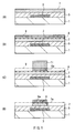
- FIG. 1 and FIG. 2A are sectional process drawings of a first example of applying a method of manufacturing a thin film transistor according to a first embodiment of the present invention to manufacture of a top-contact bottom-gate structure.
- FIG. 3 is a plan view of a thin film transistor of the top-contact bottom-gate structure manufactured in the example.
- a gate electrode 3 is formed in a pattern on an insulating substrate 1
- a gate insulating film 5 is formed so as to cover the gate electrode 3 and, further, an organic semiconductor layer 7 is formed on the gate insulating film 5.
- the processes are performed in a normal procedure, for example, as follows.
- the gate electrode 3 is formed in a pattern, for example, by forming a metal material film of gold (Au), platinum (Pt), silver (Ag), tungsten (W), tantalum (Ta), molybdenum (Mo), aluminum (Al), chromium (Cr), titanium (Ti), copper (Cu), nickel (Ni), or the like.
- the metal material film is formed by, for example, sputtering, vapor deposition, plating, or the like.
- a resist pattern (not shown) is formed on the metal material film by photolithography. Using the resist pattern as a mask, the metal material film is etched to obtain the gate electrode 3.
- the method of forming the gate electrode 3 is not limited to the above-described method but printing or the like may be applied.
- the gate insulating film 5 is made of an inorganic material such as silicon oxide or silicon nitride, the gate insulating film 5 is formed by CVD or sputtering.
- the gate insulating film 5 is made of an organic highpolymer material such as polyvinylphenol, PMMA, polyimide, fluorine resin, or the like, the gate insulating film 5 is formed by coating or printing.
- the organic semiconductor layer 7 is formed by applying a film forming method which is properly selected according to a material used.
- Examples of the organic semiconductor material to be used are as follows.
- the organic semiconductor layer 7 made of any of the above materials may be formed by applying a method properly selected from the vacuum deposition methods such as resistance heating evaporation and sputtering and the coating method such as spin coating in accordance with a material to be used.
- the coating method include air doctor coating, blade coating, rod coating, knife coating, squeeze coating, reverse roll coating, transfer roll coating, gravure coating, kiss coating, cast coating, spray coating, slit orifice coating, calendar coating, and dip coating.
- a film made of pentacene and having a thickness of 50 nm is formed by vacuum evaporation.
- the protection film 9 is made of, for example, a metal material.
- the metal material of the protection film 9 include gold (Au), platinum (Pt), palladium (Pd), silver (Ag), tungsten (W), tantalum (Ta), molybdenum (Mo), aluminum (Al), chromium (Cr), titanium (Ti), copper (Cu), nickel (Ni), indium (In), tin (Sn), manganese (Mn), ruthenium (Rh), rubidium (Rb), and their compounds.
- the protection film 9 may have a stacked structure of the above-described materials.
- the protection film 9 may be formed by applying a method properly selected from the resistance heating evaporation, the vacuum deposition method such as sputtering, or the above-described various coating methods.
- a film made of gold (Au) is formed by vacuum deposition as the protection film 9.
- a metal material component A of the protection film 9 is slightly diffused into the surface layer of the organic semiconductor layer 7.
- a resist pattern 11 is formed on the protection film 9 in a position above the gate electrode 3.
- the resist pattern 11 is formed by applying the lithography method or the printing method.
- the printing method ink jet printing, screen printing, offset printing, gravure printing, flexographic printing, micro-contact printing, or the like may be used.
- the organic semiconductor layer 7 is protected by the protection film 9.
- the protection film 9 is etched to form a protection film pattern 9a on the organic semiconductor layer 7.
- etching for the protection film 9 wet etching is employed herein.
- etchant for example, a solution made of acid such as nitric acid, sulfuric acid, hydrochloric acid, acetic acid, oxalic acid, hydrofluoric acid, or hydrogen peroxide, salt such as ammonium fluoride, potassium iodide, permanganate, or bichromate, or mixture of the acid and the salt is used.
- concentration of acids in the etchant is preferably 20% or less.
- an additive such as an organic nitrogen compound may be added.
- the resist pattern 11 is removed.
- the resist pattern 11 is removed by dissolution cleaning removal by a wet process or ashing (dry etching).
- the organic semiconductor layer 7 is protected by the protection film 9.
- the organic semiconductor layer 7 is etched and, in a state where a part on the gate electrode 3 is covered in the width direction of the gate electrode 3, an organic semiconductor pattern 7a is formed by dry etching in this case. By the process, the thin film transistor to be formed is isolated.
- the protection film pattern 9a is peeled off.
- the peel-off of the protection film pattern 9a is performed by wet etching.
- An etchant similar to that used at the time of forming the protection film pattern 9a by etching the protection film 9 is used.
- an electrode material film 13 is formed on the gate insulating film 5.
- the electrode material film 13 is provided to form a source electrode and a drain electrode and is made of a material, in a metal material or an organic conductive material, by which the film is formed without damaging the organic semiconductor pattern 7a and is in ohmic-contact with the organic semiconductor pattern 7a.
- the same material as that of the protection film 9 is used, and the electrode material film 13 is formed similarly.
- gold Au
- platinum Pt
- silver Au
- copper Cu
- aluminum Al
- nickel Ni
- chromium Cr
- molybdenum Mo
- alloys and oxides of those elements, and the like are preferably used.
- a film made of gold (Au) is formed as the electrode material film 13 by the vacuum deposition method.
- a resist pattern 15 is formed on the electrode material film 13.
- the resist pattern 15 is formed by applying the lithography or printing method.
- the printing method ink jet printing, screen printing, offset printing, gravure printing, flexographic printing, micro-contact printing, or the like may be used.
- the organic semiconductor pattern 7a is protected by the electrode material film 13.
- the electrode material film 13 is etched.
- a source electrode 13s and a drain electrode 13d are formed, which are isolated from each other above the organic semiconductor pattern 7a and have a shape that an end portion is stacked on the organic semiconductor pattern 7a in positions where they face each other while sandwiching the gate electrode 3.
- etching for the electrode material film 13 wet etching is employed.
- etchant an etchant similar to that for the protection film 9 is used.
- an etchant component B in the etchant is slightly diffused in the surface layer of the semiconductor pattern 7a.
- the resist pattern 15 is removed. Removal of the resist pattern 15 is performed in a manner similar to that of the resist pattern 11.
- an end face of each of the source electrode 13s and the drain electrode 13d isolated from each other above the organic semiconductor pattern 7a has a shape which is isotropically etched by wet etching.
- the source electrode 13s and the drain electrode 13d are shaped by etching the electrode material film 13 using the resist pattern 15 as a mask. Consequently, the source electrode 13s and the drain electrode 7s patterned with high precision may be formed.
- the etching for the electrode material film 13 is wet etching, thereby preventing the organic semiconductor pattern 7a as an under layer from being damaged. Further, since the process is an etching process using the resist pattern as a mask, it is easy and is also suitable to increase the area.
- the thin film transistor 20-1 having the top-contact structure with suppressed deterioration is obtained with high precision without damaging the organic semiconductor pattern 7a.
- the metal material component A of the protection film 9 slightly diffused in the surface layer of the organic semiconductor pattern 7a, corrosion caused by the etchant of the organic semiconductor pattern 7a is prevented. That is, the metal material component expresses corrosion prevention action against the etchant. Therefore, the film quality of the organic semiconductor pattern 7a is maintained, and excellent transistor characteristics are obtained in the thin film transistor 20-1 using the organic semiconductor pattern 7a. Further, since the metal material component A remains slightly in the surface layer of the organic semiconductor pattern 7a, an effect that the effective channel length of the thin film transistor becomes shorter is also expected.
- the etchant component B in the etchant is slightly diffused in the surface layer of the semiconductor pattern 7a. Therefore, an effect that ohmic contact between the organic semiconductor pattern 7a and the source electrode 13s and the drain electrode 13d is realized by the etchant component B is also expected.
- FIG. 4 is a sectional process drawing expressing a characteristic part of a method of manufacturing a thin film transistor according to a second embodiment.
- the second embodiment is similar to the first embodiment except that the organic semiconductor pattern 7a is over-etched.
- the source electrode 13s and the drain electrode 13d are formed. Those processes are similar to those described in the first embodiment with reference to FIGs. 1(A) to 2(C) .
- a process of removing the surface layer of the organic semiconductor pattern 7a is performed.
- over-etching of removing the surface layer of the organic semiconductor pattern 7a by dry etching is performed.
- the resist pattern 15 is peeled off and removed.
- the peeling of the resist pattern 15 may be performed in a manner similar to the first embodiment.
- an end face of each of the source electrode 13s and the drain electrode 13d isolated from each other above the organic semiconductor pattern 7s has a shape which is isotropically etched by wet etching in a manner similar to the first embodiment.
- the surface layer of the organic semiconductor pattern 7a exposed from the source electrode 13s and the drain electrode 13d is over-etched and has a slightly recessed shape.
- the source electrode 13s and the drain electrode 13d are shaped by etching the electrode material film 13 using the resist pattern 15 as a mask. Consequently, in a manner similar to the first embodiment, while applying the process which is easy and suitable for increase in the area, the thin film transistor 20-2 having the top-contact structure with suppressed deterioration is obtained with high precision without damaging the organic semiconductor pattern 7a.
- the surface layer in this part is removed by over-etching. Consequently, occurrence of parasitic transistor or the like is suppressed, and reliability of the device improves.
- FIG. 5 is a sectional process drawing expressing a characteristic part of a method of manufacturing a thin film transistor according to a third embodiment.
- the third embodiment is similar to the foregoing embodiments except that the protection film pattern 9a is left on the organic semiconductor pattern 7a.
- the organic semiconductor pattern 7a is formed. Those processes are performed in a manner similar to those described in the first embodiment with reference to FIGs. 1(A) to 1(D) .
- the material of the protection film pattern 9a a material by which a film is formed without damaging the organic semiconductor layer 7 and which comes into ohmic contact with the organic semiconductor layer 7a is selected and used.
- the protection film pattern 9a made of the metal material is provided in contact with the organic semiconductor layer 7, the metal material component A of the protection film pattern 9 is slightly diffused in the surface layer of the organic semiconductor layer 7.
- the third embodiment is characterized in that, after that, as shown in FIG. 5(B) , without removing the protection film pattern 9a, the organic semiconductor pattern 7a and the protection film pattern 9a are covered with the electrode material film 13.
- the electrode material film 13 is formed in a manner similar to the first embodiment explained with reference to FIG. 2(A) .
- the material of the electrode material film 13 may be selected without necessity of considering damage at the time of film formation on the organic semiconductor pattern 7a and ohmic contact with the organic semiconductor pattern 7a.
- the electrode material film 13 may be made of the same material as that of the protection film pattern 9a or may be made of a different material.
- the resist pattern 15 is formed on the electrode material film 13 in a manner similar to the first embodiment.
- the electrode material film 13 is etched first.
- the source electrode 13s and the drain electrode 13d are formed, which are isolated from each other above the organic semiconductor pattern 7a and have a shape that an end portion is stacked on the organic semiconductor pattern 7a in positions where they face each other while sandwiching the gate electrode 3.
- the protection film pattern 9a is etched following the etching for the electrode material film 13, the protection film pattern 9a is etched. With the etching, the protection film pattern 9a made of the metal material is left in parts where the source electrode 13s and the drain electrode 13d are stacked on the organic semiconductor pattern 7a, and by the parts where the protection film pattern 9a is left, a part of the source electrode 13s and a part of the drain electrode 13d is made thick.
- the electrode material film 13 and the protection film pattern 9a are etched by wet etching.
- etchant an etchant similar to that for the protection film 9 and the electrode material film 13 is used.
- the metal material component A of the protection film 9 slightly diffused into the surface layer of the organic semiconductor pattern 7a, corrosion caused by the etchant for the organic semiconductor pattern 7a is prevented.
- the etchant component B in the etchant is slightly diffused in the surface layer of the semiconductor pattern 7a.
- the resist pattern 15 is removed. Removal of the resist pattern 15 is performed in a manner similar to that of the resist pattern 11.
- a thin film transistor 20-3 having the top-contact bottom-gate structure shown in FIGs. 5D and 3 is obtained.
- an end face of each of the source electrode 13s and the drain electrode 13d isolated from each other above the organic semiconductor pattern 7a has a shape which is isotropically etched by wet etching.
- the parts stacked on the organic semiconductor pattern 7a in the source electrode 13s and the drain electrode 13d in the thin film transistor 20-3 are thickened.
- the parts are thickened by stacking the part made by the electrode material film 13 on the protection film pattern 9a which is in ohmic contact with the organic semiconductor pattern 7a.
- the source electrode 13s and the drain electrode 13d are shaped by etching the electrode material film 13 and the protection film pattern 9a using the resist pattern 15 as a mask. Consequently, in a manner similar to the first embodiment, while applying the process which is easy and suitable for increase in the area, the thin film transistor 20-3 having the top-contact structure with suppressed deterioration is obtained with high precision without damaging the organic semiconductor pattern 7a.
- the source electrode 13s and the drain electrode 13d part formed by the electrode material film 13 may be selected without considering the ohmic contact. Consequently, as the material of the source electrode 13s and the drain electrode 13d, a cheap material may be used and the cost may be reduced.
- the source electrode 13s and the drain electrode 13d part stacked on the organic semiconductor pattern 7a is generally formed with small line width, the part is thickened by the protection film pattern 9, so that the structure is reinforced.
- the metal material component A of the protection film 9 slightly diffused in the surface layer of the organic semiconductor pattern 7a, corrosion caused by the etchant for the organic semiconductor pattern 7a is prevented, and an effect that the thin film transistor 20-3 obtains excellent characteristics is also expected. Further, an effect is also expected that because of slight residual of the metal material component A in the surface layer of the organic semiconductor pattern 7a, the effective channel length of the thin film transistor becomes shorter.
- the etchant component B in the etchant is slightly diffused in the surface layer of the semiconductor pattern 7a. Consequently, in a manner similar to the first embodiment, an effect is expected that ohmic contact between the organic semiconductor pattern 7a and the source electrode 13s and the drain electrode 13d is realized by the etchant component B.
- the surface layer exposed in the organic semiconductor pattern 7s may be over-etched. Therefore, even in the case where the organic semiconductor pattern 7a is damaged at the time of wet etching performed for forming the source electrode 13s and the drain electrode 13d, the surface layer in this part is removed by over-etching. Consequently, occurrence of parasitic transistor or the like is suppressed, and reliability of the device improves.
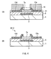
- FIGs. 6 and 7 are sectional process drawings expressing a characteristic part of a method of manufacturing a thin film transistor according to a fourth embodiment.
- the fourth embodiment is similar to the foregoing embodiments except that a carrier injection material is used for a protection film and a protection film pattern and is left.
- the gate electrode 3 is formed in a pattern on the insulating substrate 1, the gate insulating film 5 is formed so as to cover the gate electrode 3 and, further, the organic semiconductor layer 7 is formed on the gate insulating film 5.
- the processes are similar to those described in the first embodiment with reference to FIG. 1(A) and are performed by a normal procedure.
- a protection film 9' made of the carrier injection material is formed on the organic semiconductor layer 7.
- the carrier injection material for example, when a thin film transistor to be formed is of the p-channel type, an organic material of a hole injection type may be used.
- the material include poly(3,4-ethylenedioxythiophene)/poly(4-styrenesulphonate) (PEDOT/PSS), tetrathiofulvalene/tetracyanoquinodimethane) (TTF/TCNQ), tetrafluoro-tetracyanoquinodimethane (F4 TCNQ).
- the protection film 9' as such may be formed by applying a method properly selected from the vacuum deposition methods such as resistance heating evaporation and sputtering and the above-described various methods in accordance with a material to be used.
- the resist pattern 11 is formed in a manner similar to the first embodiment on the protection film 9' in a position where it overlays the gate electrode 3.
- the protection film 9' and the organic semiconductor layer 7 are etched.
- the protection film 9' and the organic semiconductor layer 7 are continuously etched by dry etching, thereby forming a protection film pattern 9a' made of the carrier injection material.
- the organic semiconductor pattern 7a is formed in a pattern so as to cover a part of the gate electrode 3 in the width direction of the gate electrode 3, and the thin film transistor is isolated.
- the resist pattern 11 is removed.
- the protection film 9' may be etched by wet etching.
- an orthogonal solvent for the organic semiconductor layer like alcohol such as ethanol or water is used.
- the electrode material film 13 may be formed in a manner similar to the first embodiment described with reference to FIG. 2(A) .
- the electrode material film 13 is made of a material which is in ohmic contact with the protection film pattern 9'.
- gold (Au), platinum (Pt), silver (Ag), copper (Cu), aluminum (Al), nickel (Ni), chromium (Cr), molybdenum (Mo), alloys and oxides of those elements, and the like are preferably used.
- the resist pattern 15 is formed on the electrode material film 13 in a manner similar to the first embodiment. Further, using the resist pattern 15 as a mask, the electrode material film 13 is etched. By the operation, the source electrode 13s and the drain electrode 13d are formed in a shape that an end portion is stacked on the organic semiconductor pattern 7a in positions where the electrodes face each other while sandwiching the gate electrode 3.
- wet etching is employed in a manner similar to the first embodiment.
- the organic semiconductor pattern 7a is not corroded by an etchant.
- reliability of the TFT is assured.
- the resist pattern 15 is removed in a manner similar to the first embodiment.
- a thin film transistor 20-4 having the top-contact bottom-gate structure shown in FIGs. 7(C) and 3 is obtained.
- the thin film transistor 20-4 obtained in such a manner, an end face of each of the source electrode 13s and the drain electrode 13d isolated from each other above the organic semiconductor pattern 7a has a shape which is isotropically etched by wet etching.
- the thin film transistor 20-4 is obtained by stacking the protection film pattern 9a' made of the carrier injection organic material on the organic semiconductor pattern 7a. Then, the protection film pattern 9a' is sandwiched between the organic semiconductor pattern 7a and the source electrode 13s and the drain electrode 13d.
- the source electrode 13s and the drain electrode 13d are shaped by etching the electrode material film 13 using the resist pattern 15 as a mask. Consequently, in a manner similar to the first embodiment, while applying a process which is easy and also suitable to increase the area, the thin film transistor 20-4 having the top-contact structure with suppressed deterioration is obtained with high precision without damaging the organic semiconductor pattern 7a.
- the organic semiconductor pattern 7a is protected with the protection film pattern 9a'.
- the film quality of the organic semiconductor pattern 7a is maintained excellently, and excellent transistor characteristics are obtained in the thin film transistor 20-4 using the organic semiconductor pattern 7a.
- the option of the electrode material film 13 enlarges, and cost may be reduced using a cheaper material.
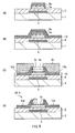
- FIGs. 8 and 9 are sectional process drawings expressing a characteristic part of a method of manufacturing a thin film transistor according to a fifth embodiment.
- the fifth embodiment is similar to the foregoing embodiments except that a protection film pattern having a stacked structure is left.
- the gate electrode 3 is formed in a pattern on the insulating substrate 1, the gate insulating film 5 is formed so as to cover the gate electrode 3 and, further, the organic semiconductor layer 7 is formed on the gate insulating film 5.
- the processes are similar to those described in the first embodiment with reference to FIG. 1(A) and are performed by a normal procedure.
- a first protection film 9' made of the carrier injection material is formed on the organic semiconductor layer 7 and, further, a second protection film 9 made of a metal material is formed.
- the first protection film 9' made of the carrier injection material is formed in a manner similar to the protection film 9' made of the carrier injection material described in the process of FIG. 6(A) of the fourth embodiment.
- the second protection film 9 made of the metal material is formed in a manner similar to the protection film made of the metal material described with reference to FIG. 1(B) in the first embodiment.
- a material which is ohmic contact with a first protection film pattern 9a-1 made of the carrier injection material is selectively used.
- the resist pattern 11 is formed in a manner similar to the first embodiment on the second protection film 9 in a position where it overlaps the gate electrode 3 and, subsequently, the second protection film 9 is etched using the resist pattern 11 as a mask.
- the second protection film 9 made of the metal material is etched by wet etching in a manner similar to the first embodiment.
- the first protection film 9' is etched.
- a protection film pattern 9A obtained by stacking a first protection film pattern 9a-1 made of the carrier injection material and a second protection film pattern 9a-2 made of a metal material in order on the organic semiconductor layer 7 is formed.
- the first protection film 9' made of the carrier injection material is etched by dry etching in a manner similar to the fourth embodiment.
- the organic semiconductor layer 7a is etched, and the organic semiconductor pattern 7a is formed in a state where a part of the gate electrode 3 is covered in the width direction of the gate electrode 3.
- the organic semiconductor layer 7a is etched by the same process as the dry etching of the first protection film 9', thereby isolating a thin film transistor to be formed.
- the resist pattern 11 is removed.
- Etching of the first protection film 9' made of the carrier injection material may be wet etching.
- an orthogonal solvent for the organic semiconductor layer like alcohol such as ethanol or water is used.
- the protection film pattern 9A is covered with the electrode material film 13.
- the electrode material film 13 is formed in a manner similar to the first embodiment described with reference to FIG. 2A .
- the resist pattern 15 is formed on the electrode material film 13 in a manner similar to the first embodiment. Further, using the resist pattern 15 as a mask, the electrode material film 13 is etched. By the operation, the source electrode 13s and the drain electrode 13d are formed in a shape that an end portion is stacked on the organic semiconductor pattern 7a in positions where the electrodes face each other while sandwiching the gate electrode 3.
- the second protection film pattern 9a-2 made of a metal material is etched.
- the second protection film pattern 9a-2 made of a metal material is left in parts in which the source electrode 13s and the drain electrode 13d are stacked on the organic semiconductor pattern 7a.
- a part of the source electrode 13s and the drain electrode 13d is thickened.
- the electrode material film 13 and the second protection film pattern 9a-2 made of a metal material are etched by wet etching.
- an etchant an etchant similar to that used in the etching of the protection film 9 and the electrode material film 13 is used.
- the resist pattern 15 is removed.
- the resist pattern 15 is removed in a manner similar to the above-described removal of the resist pattern 11.
- an end face of each of the source electrode 13s and the drain electrode 13d isolated from each other above the organic semiconductor pattern 7a has a shape which is isotropically etched by wet etching like in the first embodiment.
- the thin film transistor 20-5 is obtained by stacking the first protection film pattern 9a-1 made of the carrier injection organic material on the organic semiconductor pattern 7a.
- a part stacked on the organic semiconductor pattern 7a in the source electrode 13s and the drain electrode 13d is thickened by the second protection film pattern 9a-2 made of the metal material.
- the source electrode 13s and the drain electrode 13d are shaped by etching the electrode material film 13 using the resist pattern 15 as a mask. Consequently, in a manner similar to the first embodiment, while applying a process which is easy and also suitable to increase the area, the thin film transistor 20-4 having the top-contact structure with suppressed deterioration is obtained with high precision without damaging the organic semiconductor pattern 7a.
- the film quality of the organic semiconductor pattern 7a is maintained excellently by being protected by the first protection film pattern 9a-1 made of the carrier injection material, and excellent transistor characteristics are obtained in the thin film transistor 20-4 using the organic semiconductor pattern 7a. Further, since formation of the electrode material film 13 and the second protection film 9 made of the metal material does not exert influence on the organic semiconductor pattern 7a, the option of the electrode material film 13 enlarges, and cost may be reduced using a cheaper material.
- the source electrode 13s and the drain electrode 13d part formed by the electrode material film 13 may be selected without considering the ohmic contact. Consequently, as the material of the source electrode 13s and the drain electrode 13d, a cheap material may be used and the cost may be reduced.
- the source electrode 13s and the drain electrode 13d part stacked on the organic semiconductor pattern 7a is generally formed with small line width, the part is thickened by the second protection film pattern 9a-2, so that the structure is reinforced.
- the configuration of forming the organic semiconductor pattern 7a by formation of an organic semiconductor layer and patterning of the formed organic semiconductor layer has been described.
- the formation of the semiconductor pattern 7a is not limited to the procedure but may be the following methods. For example, patterning by vapor deposition using a metal mask, patterning using a print shadow mask, patterning by liftoff process, further, patterning to which a printing method such as ink jet printing, reverse offset printing, or microcontact printing is applied, and the like may be applied.
- patterning by vapor deposition using a metal mask patterning using a print shadow mask, patterning by liftoff process, further, patterning to which a printing method such as ink jet printing, reverse offset printing, or microcontact printing is applied, and the like may be applied.
- the thin film transistor of the top contact type using organic semiconductor as a channel is stably realized.
- the contact resistance between the organic semiconductor layer and the source-drain electrode has to be reduced further. This is because, even when semiconductor of high mobility is used, if the contact resistance is high, mobility of an entire device is limited.
- One of methods of reducing contact resistance is a method of increasing carrier injection efficiency by controlling the work function of the electrode material by electrode modification or the like. It is however difficult to introduce such a technique in the organic thin film transistor of the top contact type. In the following embodiment, the method of increasing carrier mobility by reducing the contact resistance between the organic semiconductor layer and the source and drain electrode will be described.
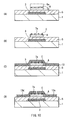
- FIG. 10 is a sectional process drawing expressing a characteristic part of a method of manufacturing a thin film transistor according to a sixth embodiment. Since the processes of the sixth embodiment are the same as those of the first embodiment up to the process of FIG. 2(A) , the subsequent processes will be described.
- a surface process is performed with a surface treatment agent on the surface of the organic semiconductor pattern 7a.
- the surface treatment agent contains molecules which chemically react with the metal material such as gold (Au) remaining in the surface layer of the organic semiconductor pattern 7a.
- the molecule include organosulfur molecules of thiols, disulfides, and the like, organic selenium/tellurium molecules, nitrile compound, organic silane compound, carboxylic acids, phosphonic acids, phosphoesters, unsaturated hydrocarbons, alcohol aldehyde, halide, diazo compound, and the like.
- the surface treatment may be performed in a gas phase or in a solution.
- pentafluorobenzenethiol is used as the surface treatment agent.
- reaction between gold (Au) A remaining in the surface layer of the organic semiconductor pattern 7a and a thiol molecule C is made.
- the gold molecule A and the thiol molecule C are chemically combined, and contact resistance between the source electrode 13s and the drain electrode 13d formed by the same Au later and the organic semiconductor pattern 7a is reduced.
- the thiol molecules C are dispersed in this case, they may be formed in a layer state on the surface of the organic semiconductor pattern 7a.
- the electrode material film 13 made of, for example, Au is formed on the gate insulating film 5 so as to cover the organic semiconductor pattern 7a.
- the process is similar to that of FIG. 2(B) , the details will not be repeated.
- a resist pattern (not shown) is formed on the electrode material film 13 and, using the resist pattern as a mask, the electrode material film 13 is etched. By the etching, the source electrode 13s and the drain electrode 13d are formed. After that, the resist pattern is removed.
- the surface of the organic semiconductor pattern 7a is subjected to surface treatment with tetrafluorobenzenethiol to make reaction between Au residing in the surface of the organic semiconductor pattern 7a and tetrafluorobenzenethiol.
- contact resistance between the organic semiconductor pattern 7a and each of the source electrode 13s and the drain electrode 13d is reduced, and the carrier mobility may be increased. Therefore, to the fields requiring high mobility, an organic thin film transistor of the top contact type is applied. The other effects are similar to those of the first embodiment.
- FIG. 11 illustrates the relation between gate voltage (V) and drain current (A) in the case where the drain voltage is set to -12V, of each of a thin film transistor (example 1) subjected to the surface treatment by the embodiment and a thin film transistor (comparative example) obtained without the surface treatment.
- the parameters are the same except for the presence or absence of the surface treatment.
- P1 illustrates the example 1
- P2 illustrates the comparative example.
- the contact resistance of the comparative example is 6.8 k ⁇ cm and, in contrast, that of the example 1 is 2.7 k ⁇ cm. It is understood that the contact resistance is largely reduced as compared with that of the comparative example.
- FIG. 12 is a sectional process drawing expressing a characteristic part of a method of manufacturing a thin film transistor according to a seventh embodiment.
- an organic complex pattern as a carrier injection layer is interposed between the organic semiconductor pattern 7a and each of the source electrode 13s and the drain electrode 13d. Since the processes of the seventh embodiment are also the same as those of the first embodiment up to the process of FIG. 2(A) , the subsequent processes will be described.
- a mask 21 made of metal is formed on the organic semiconductor pattern 7a by photolithography or printing.
- the protection film pattern 9a may not be peeled off but may be patterned by being partially etched and used.
- an organic charge-transfer complex is formed on the gate insulating film 5 so as to cover the organic semiconductor pattern 7a and the mask 21, thereby forming an organic charge-transfer complex film 22.
- the organic charge-transfer complex may be a charge-transfer complex of an organic donor and an organic acceptor such as TTF-TCNQ, or a charge-transfer complex of an organic molecule and an inorganic ion compound (pentacene-metal oxide).
- a method of forming the organic charge-transfer complex vacuum deposition of a complex or co-deposition of a donor and an acceptor may be mentioned. Alternatively, any of the above-described various printing methods may be used.
- the organic charge-transfer complex has a composition of (D: donor) x - (A: acceptor) y.
- the donor molecule examples include polypyrrole and polypyrrole substitute, polythiophene and polythiophene substitute, isothianaphthenes such as polyisothianaphthene, chenylene vinylenes such as polychenylene vinylene, poly(p-phenylenevinylenes) such as poly(p-phenylenevinylene), polyaniline and polyaniline substitute, polyacetylenes, polydiacetylenes, polyazulenes, polypyrenes, polycarbazoles, polyselenophenes, polyfurans, poly(p-phenylenes), polyindoles, polypyridazines, polymers and polycyclic condensate such as polyvinyl carbazole, polyphenylene sulfide, or polyvinylene sulfide, derivatives (triphenodioxazine, triphenodithiazine, hexacene-6, 15-quinone, or the
- acceptor molecule examples include a benzene diquinone derivative such as DDQ or chloranil and its analog, a cyanoquinodimethane derivative such as DCNQI or TCNQ and its analog, a metal complex such as M(mnt)2 or M(dmit)2 (where M denotes metal atom), naphthalene 1,4,5,8-tetracarboxylic acid diimide, N,N'-bis(4-trifuoromethyl benzyl) naphthalene 1,4,5,8-tetracarboxylic acid diimide, N,N'-bis(1H, 1H-perfluorooctyl), N,N'-bis(1H, 1H-perfluorooctyl), and N,N'-dioctylnaphthalene 1,4,5,8-tetracarboxylic acid diimide derivative, naphthalene tetracarboxylic acid diimides such as
- the pattern of the organic charge-transfer complex film 22 is formed.
- the electrode material film 13 made of, for example, Au is formed on the gate insulating film 5.
- a resist pattern (not shown) is formed on the electrode material film 13 and, by etching the electrode material film 13 using the resist pattern as a mask, the source electrode 13s and the drain electrode 13d are formed. After that, the resist pattern is removed.
- the pattern of the organic charge-transfer complex film 22 is formed on the surface of the organic semiconductor pattern 7a. Therefore, the organic charge-transfer complex film 22 functions as the carrier injection layer between the organic semiconductor pattern 7a and each of the source electrode 13s and the drain electrode 13d.
- the contact resistance between the organic semiconductor pattern 7a and each of the source electrode 13s and the drain electrode 13d is reduced, and the carrier mobility may be increased. Therefore, also in the embodiment, to the fields requesting high mobility, the organic thin film transistor of the top contact type is applied. The other effects are similar to those of the first embodiment.
- the area ratio between the source electrode 13s and the drain electrode 13d and the organic charge-transfer complex film 22 on the organic semiconductor pattern 7a is not limited.
- the entire organic charge-transfer complex film 22 may be hidden below each of the electrodes or a part of the organic charge-transfer complex film 22 may be out of each of the electrodes.
- the organic complex below the source electrode 13s and that below the drain electrode 13d are not in contact with each other.
- FIG. 13 is a sectional process drawing expressing a characteristic part of a method of manufacturing a thin film transistor according to an eighth embodiment.
- the pattern of the organic charge-transfer complex film 22 is formed by using the mask 21 made of a metal.
- an insulating mask 23 made of, for example, SiO 2 is used at the time of forming the organic charge-transfer complex film 22 at the time of forming the organic charge-transfer complex film 22.
- the mask 23 is left in the structure ( FIG. 13(C) ), so that the manufacturing process is simplified. Since the rest is the same as the seventh embodiment, the description will not be repeated.
- FIG. 14 is a circuit configuration diagram of a display device (electronic device) 30.
- a display region 1a and a peripheral region 1b are set on the substrate 1 of a display device 30, a display region 1a and a peripheral region 1b are set.
- a plurality of scanning lines 31 are disposed laterally and a plurality of signal lines 33 are disposed vertically.
- the display region 1a is constructed as a pixel array in which one pixel "a" is provided in correspondence with each of intersection points of the scan lines 31 and the signal lines 33.
- a scanning line drive circuit 35 for driving the scanning lines 31 and a signal line drive circuit 37 for supplying a video signal (that is, input signal) according to brightness information to the signal lines 33 are disposed.
- a pixel circuit provided at each of the intersecting points of the scanning lines 31 and the signal lines 33 is constructed by, for example, a thin film transistor Tr1 for switching, a thin film transistor Tr2 for driving, a retention capacitor Cs, and an organic electroluminescence element EL.
- a thin film transistor Tr1 for switching a thin film transistor Tr2 for driving
- a retention capacitor Cs a retention capacitor
- an organic electroluminescence element EL an organic electroluminescence element EL.
- the display device 30 by driving of the scanning line drive circuit 35, a video signal written from the signal line 33 via the thin film transistor Tr1 for switching is held in the retention capacitor Cs. Current according to the amount of signal held is supplied from the thin film transistor Tr2 for driving to the organic electroluminescence element EL, and the organic electroluminescence element EL emits light with brightness according to the current value.
- the thin film transistor Tr2 for driving is connected to a common power supply line (Vcc) 39.
- a capacitive element may be provided in the pixel circuit or a pixel circuit may be constructed by providing a plurality of transistors. To the peripheral region 1b, a necessary drive circuit is added according to change in the pixel circuit.
- FIG. 15 expresses a sectional structure of the display device 30 having the above-described circuit configuration.
- the diagram illustrates a structure of one pixel in which the thin film transistors Tr2 and Tr1, the capacitive element Cs, and the organic electroluminescence element EL are stacked.
- the diagram illustrates an example of providing the thin film transistor 20-1 having the top-contact bottom-gate structure shown in FIG. 2D in the first embodiment as the thin film transistors Tr2 and Tr1 provided for each pixel "a".
- the source electrode 13s of the thin film transistor Tr1 and the gate electrode 3 of the thin film transistor Tr2 are connected to each other via a connection hole 5a provided for the gate insulating film 5.
- the capacitive element Cs is constructed by making the gate insulating film 5 sandwiched between an extension part of the gate electrode 3 in the thin film transistor Tr2 and an extension part of the source electrode 13s.
- the gate electrode 3 of the thin film transistor Tr1 is extended to the scanning line 31
- the drain electrode 13d of the thin film transistor Tr1 is extended to the signal line 33
- the source electrode 13s of the thin film transistor Tr2 is extended to the power supply line 39.
- the thin film transistors Tr1 and Tr2 and the capacitive element Cs are covered, for example, with an interlayer insulating film 41 via a protection film.
- the interlayer insulating film 41 is preferably constructed as a planarized film.
- the interlayer insulating film 41 is provided with a connection hole 41a reaching the drain electrode 13d of the thin film transistor Tr2.
- Each of the pixels on the interlayer insulating film 41 is provided with the organic electroluminescence element EL connected to the thin film transistor Tr2 via the connection hole 41 a.
- the organic electroluminescence element EL is isolated by an insulating pattern 43 provided on the interlayer insulating film 41.
- the organic electroluminescence element EL has a pixel electrode 45 provided on the interlayer insulating film 41.
- the pixel electrode 45 is formed as a conductive pattern for each pixel and is connected to the drain electrode 13d of the thin film transistor Tr2 via the connection hole 41 a provided for the interlayer insulating film 41.
- Such a pixel electrode 45 is used as, for example, an anode.
- the periphery of the pixel electrode 45 is covered with the insulating pattern 43 for isolating the organic electroluminescence element EL.
- the insulating pattern 43 has an open window 43a for widely exposing the pixel electrode 45.
- the open window 43a serves as a pixel opening of the organic electroluminescence element EL.
- An organic layer 47 is provided so as to cover the pixel electrode 45 exposed from the insulating pattern 43.
- the organic layer 47 has a stacked structure having at least an organic light emission layer and is obtained by stacking, as necessary, a hole injection layer, a hole transport layer, an organic light emission layer, an electron transport layer, an electron injection layer, and other layers in order from an anode (the pixel electrode 45) side.
- a common electrode 49 is provided so as to cover the organic layer 47 and sandwich the organic layer 47 between the pixel electrode 45 and itself.
- the common electrode 49 is an electrode on the side of extracting light generated by the organic light emission layer in the organic electroluminescence element EL and is made of a material having light transmitting property.
- the pixel electrode 45 functions as an anode, so that the common electrode 49 is constructed by using a material which functions as a cathode at least on the side in contact with the organic layer 47.
- the common electrode 49 is disposed at GND.
- a pixel part in which the organic layer 47 is sandwiched between the pixel electrode 45 and the common electrod3 49 is a part functioning as the organic electroluminescence element EL.
- each organic electroluminescence element EL is covered with an encapsulation resin made of a light transmissive material, and an opposed substrate made of a light transmissive material is adhered via the encapsulation resin, the display device 30 is constructed.
- the pixel circuit is constructed by using a fine thin film transistor having excellent characteristics. Consequently, the pixel electrode 45 is stably driven and microfabrication of the pixel is achieved, so that the display characteristic improves.
- the display device of the active matrix using the organic electroluminescence element EL is illustrated.
- the electronic device of the invention is applicable widely to a display device having a thin film transistor such as a liquid crystal display device and an electrophoretic display.
- the invention is widely applicable to an electronic device having the display device.
- the invention may be applied to an electric paper, a digital camera, a notebook-sized personal computer, a portable terminal device such as a cellular phone, and an electronic device such as a video camera. That is, the invention is applicable to an electronic device having a display device in all of fields in which a video signal input to the electronic device or a video signal generated in the electronic device is displayed as an image or video image.
- the electronic device of an embodiment of the invention is not limited to the display device.
- the invention is widely applicable to an electronic device having the thin film transistor to which a conductive pattern (such as a pixel electrode) is connected.
- the invention is applicable also to electronic devices such as an ID tag and a sensor. By using a fine thin film transistor having excellent characteristics in such an electronic device, a miniaturized device is stable driven.
Landscapes
- Engineering & Computer Science (AREA)
- Manufacturing & Machinery (AREA)
- Chemical & Material Sciences (AREA)
- Nanotechnology (AREA)
- Microelectronics & Electronic Packaging (AREA)
- Physics & Mathematics (AREA)
- Mathematical Physics (AREA)
- Theoretical Computer Science (AREA)
- Crystallography & Structural Chemistry (AREA)
- Thin Film Transistor (AREA)
- Electrodes Of Semiconductors (AREA)
Abstract
Description
- The present invention relates to a method of manufacturing a thin film transistor, a thin film transistor, and an electronic device. More particularly, the invention relates to a method of manufacturing a thin film transistor in which fine source and drain electrodes are formed over an organic semiconductor pattern, a thin film transistor obtained by the method, and an electronic device using the thin film transistor.
- In recent years, attention is paid to a thin film transistor (TFT) using an organic semiconductor as a channel layer, a so-called organic TFT. Since the organic TFT is formed by applying a channel layer made of organic semiconductor at low temperature, it is advantageous to reduction of cost. The organic TFT is also formed on a flexible substrate having no heat resistance property such as a plastic substrate. It is known that, in an organic TFT having a top-contact bottom-gate structure, deterioration in characteristics due to stress of heat or the like is suppressed as compared with an organic TFT having a bottom-contact structure.
- In manufacture of such an organic TFT of the top-contact bottom-gate structure, a method of patterning a source electrode and a drain electrode with high precision on an organic semiconductor pattern is being examined. For example, Japanese Unexamined Patent Application Publication No.
2006-216718 - Patent Literature 1: Japanese Unexamined Patent Publication No.
2006-216718 - However, in the manufacturing method using the intersecting part which halves a space above a substrate, formation of the intersection part is troublesome, and it is difficult to form a source electrode and a drain electrode with uniform precision over a substrate of large area.
- Therefore, it is an object of the present invention to provide a method of manufacturing a thin film transistor of a top-contact structure with suppressed deterioration by a process which is easy and suitable for increase in area without damaging an organic semiconductor pattern. Further, it is an object of the present invention to provide a thin film transistor having a top-contact structure obtained by applying the method and, further, an electronic device having the thin film transistor.
- A method of manufacturing a thin film transistor of the present invention for achieving such objects is performed by the following procedure.
First, an organic semiconductor pattern is formed on a substrate. Next, an electrode material film is formed on the substrate so as to cover the organic semiconductor pattern. After that, a resist pattern is formed on the electrode material film, and a source electrode and a drain electrode obtained by patterning the electrode material film by wet etching using the resist pattern as a mask are formed. - In the method of manufacturing a thin film transistor, the electrode material film is etched using the resist pattern as a mask, so that the source electrode and the drain electrode patterned with high precision are formed. Since wet etching is performed as the etching of the electrode material film, the organic semiconductor layer under the electrode material film is prevented from being damaged. Further, since the etching process using the resist pattern as a mask is performed, the method is easy and suitable for increase in area.
- Moreover, a thin film transistor of the present invention is formed by the above-described method and has: an organic semiconductor pattern provided on a substrate; and a source electrode and a drain electrode provided over the substrate in a state where they are isolated from each other above the semiconductor pattern. In particular, each of the source and drain electrodes has an end face shape which is isotropically etched.
- According to a method of manufacturing a thin film transistor of the present invention, while applying a process which is easy and suitable for increase in area, a thin film transistor of a top-contact structure with suppressed deterioration is obtained with high precision without damaging an organic semiconductor pattern. By using a thin film transistor obtained in such a manner, an electrode device with suppressed deterioration is obtained.
-
- [
FIG. 1 ] Sectional process drawings (No. 1) for explaining a first embodiment of the present invention. - [
FIG. 2 ]Sectional process drawings (No. 2) for explaining the first embodiment. - [
FIG. 3 ] A schematic plan view of a thin film transistor of a top contact structure to which the present invention is applied. - [
FIG. 4 ] Sectional process drawings for explaining a characteristic part of a second embodiment. - [
FIG. 5 ] Sectional process drawings for explaining a characteristic part of a third embodiment. - [
FIG. 6 ] Sectional process drawings (No. 1) for explaining a fourth embodiment. - [
FIG. 7 ] Sectional process drawings (No. 2) for explaining the fourth embodiment. - [
FIG. 8 ] Sectional process drawings (No. 1) for explaining a fifth embodiment. - [
FIG. 9 ] Sectional process drawings (No. 2) for explaining the fifth embodiment. - [
FIG. 10 ] Sectional process drawings for explaining a sixth embodiment. - [
FIG. 11 ] A characteristic diagram for explaining an effect of the sixth embodiment. - [
FIG. 12 ] Sectional process drawings for explaining a seventh embodiment. - [
FIG. 13 ] Sectional process drawings for explaining an eighth embodiment. - [
FIG. 14 ] A circuit diagram expressing an example of application to a display device. - [
FIG. 15 ] A cross section of one pixel in the display device. - Embodiments of the present invention will be described with reference to the drawings below in the following order.
- 1. First embodiment (method of manufacturing a thin film transistor)
- 2. Second embodiment (an example of over-etching an organic semiconductor pattern)
- 3. Third embodiment (an example of leaving a protection film pattern on an organic semiconductor pattern)
- 4. Fourth embodiment (an example of using a carrier injection material as a protection film and a protection film pattern and leaving them)
- 5. Fifth embodiment (an example of using a protection film pattern as a stacking structure and leaving it)
- 6. Sixth embodiment (an example of reducing contact resistance)
- 7. Seventh embodiment (another example of reducing contact resistance)
- 8. Eighth embodiment (another example of reducing contact resistance)
- 9. Example of application to electronic device (display device)
-
FIG. 1 andFIG. 2A are sectional process drawings of a first example of applying a method of manufacturing a thin film transistor according to a first embodiment of the present invention to manufacture of a top-contact bottom-gate structure.FIG. 3 is a plan view of a thin film transistor of the top-contact bottom-gate structure manufactured in the example. In the following, according to the sectional process drawings ofFIGs. 1 and2 , referring toFIG. 3 , the manufacturing method of the first embodiment will be described. - First, as illustrated in
FIG. 1(A) , agate electrode 3 is formed in a pattern on an insulatingsubstrate 1, agate insulating film 5 is formed so as to cover thegate electrode 3 and, further, anorganic semiconductor layer 7 is formed on thegate insulating film 5. The processes are performed in a normal procedure, for example, as follows. - The
gate electrode 3 is formed in a pattern, for example, by forming a metal material film of gold (Au), platinum (Pt), silver (Ag), tungsten (W), tantalum (Ta), molybdenum (Mo), aluminum (Al), chromium (Cr), titanium (Ti), copper (Cu), nickel (Ni), or the like. The metal material film is formed by, for example, sputtering, vapor deposition, plating, or the like. After that, a resist pattern (not shown) is formed on the metal material film by photolithography. Using the resist pattern as a mask, the metal material film is etched to obtain thegate electrode 3. In addition, the method of forming thegate electrode 3 is not limited to the above-described method but printing or the like may be applied. - When the
gate insulating film 5 is made of an inorganic material such as silicon oxide or silicon nitride, thegate insulating film 5 is formed by CVD or sputtering. On the other hand, when thegate insulating film 5 is made of an organic highpolymer material such as polyvinylphenol, PMMA, polyimide, fluorine resin, or the like, thegate insulating film 5 is formed by coating or printing. - The
organic semiconductor layer 7 is formed by applying a film forming method which is properly selected according to a material used. - Examples of the organic semiconductor material to be used are as follows.
- polypyrrole and polypyrrole substitute,
- polythiophene and polythiophene substitute,
- isothianaphthenes such as polyisothianaphthene,
- chenylene vinylenes such as polychenylene vinylene,
- poly(p-phenylenevinylenes) such as poly(p-phenylenevinylene),
- polyaniline and polyaniline substitute,
- polyacetylenes,
- polydiacetylenes,
- polyazulenes,
- polypyrenes,
- polycarbazoles,
- polyselenophenes,
- polyfurans,
- poly(p-phenylenes),
- polyindoles,
- polypyridazines,
- polymers and polycyclic condensate such as polyvinyl carbazole, polyphenylene sulfide, or polyvinylene sulfide,
- derivatives (triphenodioxazine, triphenodithiazine, hexacene-6, 15-quinone, or the like) obtained by substituting oligomers having the same repeating unit as that of the polymer in the material, acenes such as naphthacene, pentacene, hexacene, dibenzopentacene, tetrabenzopentacene, pyrene, dizenzopyrene, chrysene, perylene, coronene, terrylene, ovalene, quaterrylene, and circumanthracene, and a part of carbon in the acenes with a functional group such as atoms of N, S, O, or the like, a carbonyl group, or the like,
- metal phthalocyanines,
- tetrathiafulvalene and tetrathiafulvalene derivatives,
- tetrathiapentalene and tetrathiapentalene derivatives,
-
naphthalene naphthalene dioctylnaphthalene - naphthalene tetracarboxylic acid diimides such as
naphthalene - condensed-ring tetracarboxylic acid diimides such as anthracene tetracarboxylic acid diimides like
anthracene - fullerenes such as C60, C70, C76, C78, and C84,
- carbon nanotube such as SWNT, and
- pigments such as merocyanine dyes and hemicyanine dyes.
- The
organic semiconductor layer 7 made of any of the above materials may be formed by applying a method properly selected from the vacuum deposition methods such as resistance heating evaporation and sputtering and the coating method such as spin coating in accordance with a material to be used. Examples of the coating method include air doctor coating, blade coating, rod coating, knife coating, squeeze coating, reverse roll coating, transfer roll coating, gravure coating, kiss coating, cast coating, spray coating, slit orifice coating, calendar coating, and dip coating. - Herein, for example, as the
organic semiconductor layer 7, a film made of pentacene and having a thickness of 50 nm is formed by vacuum evaporation. - Next, as shown in
FIG. 1(B) , aprotection film 9 is formed on theorganic semiconductor layer 7. Theprotection film 9 is made of, for example, a metal material. Examples of the metal material of theprotection film 9 include gold (Au), platinum (Pt), palladium (Pd), silver (Ag), tungsten (W), tantalum (Ta), molybdenum (Mo), aluminum (Al), chromium (Cr), titanium (Ti), copper (Cu), nickel (Ni), indium (In), tin (Sn), manganese (Mn), ruthenium (Rh), rubidium (Rb), and their compounds. In addition, theprotection film 9 may have a stacked structure of the above-described materials. - The
protection film 9 may be formed by applying a method properly selected from the resistance heating evaporation, the vacuum deposition method such as sputtering, or the above-described various coating methods. - Herein, for example, a film made of gold (Au) is formed by vacuum deposition as the
protection film 9. - By forming the
protection film 9 made of the metal material in contact with theorganic semiconductor layer 7 as described above, a metal material component A of theprotection film 9 is slightly diffused into the surface layer of theorganic semiconductor layer 7. - Next, as shown in
FIG. 1(C) , a resistpattern 11 is formed on theprotection film 9 in a position above thegate electrode 3. The resistpattern 11 is formed by applying the lithography method or the printing method. As the printing method, ink jet printing, screen printing, offset printing, gravure printing, flexographic printing, micro-contact printing, or the like may be used. In addition, in formation of the resistpattern 11, theorganic semiconductor layer 7 is protected by theprotection film 9. - Subsequently, using the resist
pattern 11 as a mask, theprotection film 9 is etched to form aprotection film pattern 9a on theorganic semiconductor layer 7. As the etching for theprotection film 9, wet etching is employed herein. - As etchant, for example, a solution made of acid such as nitric acid, sulfuric acid, hydrochloric acid, acetic acid, oxalic acid, hydrofluoric acid, or hydrogen peroxide, salt such as ammonium fluoride, potassium iodide, permanganate, or bichromate, or mixture of the acid and the salt is used. To suppress damage on the
organic semiconductor layer 7, the concentration of acids in the etchant is preferably 20% or less. Further, to assure stable etching rate, an additive such as an organic nitrogen compound may be added. - After the
protection film pattern 9a is formed by wet etching, the resistpattern 11 is removed. The resistpattern 11 is removed by dissolution cleaning removal by a wet process or ashing (dry etching). In addition, at the time of removing the resistpattern 11, theorganic semiconductor layer 7 is protected by theprotection film 9. - Next, as illustrated in
FIG. 1(D) , using theprotection film pattern 9a as a mask, theorganic semiconductor layer 7 is etched and, in a state where a part on thegate electrode 3 is covered in the width direction of thegate electrode 3, anorganic semiconductor pattern 7a is formed by dry etching in this case. By the process, the thin film transistor to be formed is isolated. - Next, as illustrated in
FIG. 2(A) , theprotection film pattern 9a is peeled off. The peel-off of theprotection film pattern 9a is performed by wet etching. An etchant similar to that used at the time of forming theprotection film pattern 9a by etching theprotection film 9 is used. - Next, as illustrated in
FIG. 2(B) , in a state where theorganic semiconductor pattern 7a is covered, anelectrode material film 13 is formed on thegate insulating film 5. Theelectrode material film 13 is provided to form a source electrode and a drain electrode and is made of a material, in a metal material or an organic conductive material, by which the film is formed without damaging theorganic semiconductor pattern 7a and is in ohmic-contact with theorganic semiconductor pattern 7a. The same material as that of theprotection film 9 is used, and theelectrode material film 13 is formed similarly. Particularly, from the viewpoint of ohmic-contact with theorganic semiconductor pattern 7a, gold (Au), platinum (Pt), silver (Ag), copper (Cu), aluminum (Al), nickel (Ni), chromium (Cr), molybdenum (Mo), alloys and oxides of those elements, and the like are preferably used. - In this case, for example, a film made of gold (Au) is formed as the
electrode material film 13 by the vacuum deposition method. - Next, as shown in
FIG. 2(C) , a resistpattern 15 is formed on theelectrode material film 13. The resistpattern 15 is formed by applying the lithography or printing method. As the printing method, ink jet printing, screen printing, offset printing, gravure printing, flexographic printing, micro-contact printing, or the like may be used. In addition, in formation of the resistpattern 15, theorganic semiconductor pattern 7a is protected by theelectrode material film 13. - Subsequently, using the resist
pattern 15 as a mask, theelectrode material film 13 is etched. By the operation, asource electrode 13s and adrain electrode 13d are formed, which are isolated from each other above theorganic semiconductor pattern 7a and have a shape that an end portion is stacked on theorganic semiconductor pattern 7a in positions where they face each other while sandwiching thegate electrode 3. - As the etching for the
electrode material film 13, wet etching is employed. As etchant, an etchant similar to that for theprotection film 9 is used. By an effect of the metal material component A of theprotection film 9 slightly diffused into the surface layer of theorganic semiconductor pattern 7a, corrosion caused by the etchant for theorganic semiconductor pattern 7a is prevented. Further, by the wet etching, an etchant component B in the etchant is slightly diffused in the surface layer of thesemiconductor pattern 7a. - After the
source electrode 13s and thedrain electrode 13d are formed by wet etching, the resistpattern 15 is removed. Removal of the resistpattern 15 is performed in a manner similar to that of the resistpattern 11. - As a result, a thin film transistor 20-1 having the top-contact bottom-gate structure shown in
FIGs. 2(D) and3 is obtained. - In the thin film transistor 20-1 obtained in such a manner, an end face of each of the
source electrode 13s and thedrain electrode 13d isolated from each other above theorganic semiconductor pattern 7a has a shape which is isotropically etched by wet etching. - In the first embodiment, the
source electrode 13s and thedrain electrode 13d are shaped by etching theelectrode material film 13 using the resistpattern 15 as a mask. Consequently, thesource electrode 13s and the drain electrode 7s patterned with high precision may be formed. The etching for theelectrode material film 13 is wet etching, thereby preventing theorganic semiconductor pattern 7a as an under layer from being damaged. Further, since the process is an etching process using the resist pattern as a mask, it is easy and is also suitable to increase the area. - As a result, while applying the process which is easy and suitable for increase in the area, the thin film transistor 20-1 having the top-contact structure with suppressed deterioration is obtained with high precision without damaging the
organic semiconductor pattern 7a. - Moreover, by the effect of the metal material component A of the
protection film 9 slightly diffused in the surface layer of theorganic semiconductor pattern 7a, corrosion caused by the etchant of theorganic semiconductor pattern 7a is prevented. That is, the metal material component expresses corrosion prevention action against the etchant. Therefore, the film quality of theorganic semiconductor pattern 7a is maintained, and excellent transistor characteristics are obtained in the thin film transistor 20-1 using theorganic semiconductor pattern 7a. Further, since the metal material component A remains slightly in the surface layer of theorganic semiconductor pattern 7a, an effect that the effective channel length of the thin film transistor becomes shorter is also expected. - Moreover, by the wet etching performed at the time of forming the
source electrode 13s and thedrain electrode 13d, the etchant component B in the etchant is slightly diffused in the surface layer of thesemiconductor pattern 7a. Therefore, an effect that ohmic contact between theorganic semiconductor pattern 7a and thesource electrode 13s and thedrain electrode 13d is realized by the etchant component B is also expected. -
FIG. 4 is a sectional process drawing expressing a characteristic part of a method of manufacturing a thin film transistor according to a second embodiment. The second embodiment is similar to the first embodiment except that theorganic semiconductor pattern 7a is over-etched. - First, by wet-etching the
electrode material film 13 using the resistpattern 15 as a mask, thesource electrode 13s and thedrain electrode 13d are formed. Those processes are similar to those described in the first embodiment with reference toFIGs. 1(A) to 2(C) . - In the embodiment, after that, as shown in
FIG. 4(A) , by over-etching theorganic semiconductor pattern 7a exposed from thesource electrode 13s and thedrain electrode 13d, a process of removing the surface layer of theorganic semiconductor pattern 7a is performed. In this case, over-etching of removing the surface layer of theorganic semiconductor pattern 7a by dry etching is performed. - After that, the resist
pattern 15 is peeled off and removed. The peeling of the resistpattern 15 may be performed in a manner similar to the first embodiment. - By the process, a thin film transistor 20-2 having the top-contact bottom-gate structure shown in
FIGs. 4(B) and3 is obtained. - Also in the thin film transistor 20-2 obtained in such a manner, an end face of each of the
source electrode 13s and thedrain electrode 13d isolated from each other above the organic semiconductor pattern 7s has a shape which is isotropically etched by wet etching in a manner similar to the first embodiment. In particular, the surface layer of theorganic semiconductor pattern 7a exposed from thesource electrode 13s and thedrain electrode 13d is over-etched and has a slightly recessed shape. - Also in this embodiment, the
source electrode 13s and thedrain electrode 13d are shaped by etching theelectrode material film 13 using the resistpattern 15 as a mask. Consequently, in a manner similar to the first embodiment, while applying the process which is easy and suitable for increase in the area, the thin film transistor 20-2 having the top-contact structure with suppressed deterioration is obtained with high precision without damaging theorganic semiconductor pattern 7a. - Further, particularly, even in the case where the
organic semiconductor pattern 7a is damaged at the time of wet etching performed for forming thesource electrode 13s and thedrain electrode 13d, the surface layer in this part is removed by over-etching. Consequently, occurrence of parasitic transistor or the like is suppressed, and reliability of the device improves. -
FIG. 5 is a sectional process drawing expressing a characteristic part of a method of manufacturing a thin film transistor according to a third embodiment. The third embodiment is similar to the foregoing embodiments except that theprotection film pattern 9a is left on theorganic semiconductor pattern 7a. - First, as shown in
FIG. 5(A) , by dry-etching theorganic semiconductor layer 7 over theprotection film pattern 9a made of a metal material, theorganic semiconductor pattern 7a is formed. Those processes are performed in a manner similar to those described in the first embodiment with reference toFIGs. 1(A) to 1(D) . As the material of theprotection film pattern 9a, a material by which a film is formed without damaging theorganic semiconductor layer 7 and which comes into ohmic contact with theorganic semiconductor layer 7a is selected and used. - In a manner similar to the first embodiment, since the
protection film pattern 9a made of the metal material is provided in contact with theorganic semiconductor layer 7, the metal material component A of theprotection film pattern 9 is slightly diffused in the surface layer of theorganic semiconductor layer 7. - The third embodiment is characterized in that, after that, as shown in
FIG. 5(B) , without removing theprotection film pattern 9a, theorganic semiconductor pattern 7a and theprotection film pattern 9a are covered with theelectrode material film 13. Theelectrode material film 13 is formed in a manner similar to the first embodiment explained with reference toFIG. 2(A) . However, the material of theelectrode material film 13 may be selected without necessity of considering damage at the time of film formation on theorganic semiconductor pattern 7a and ohmic contact with theorganic semiconductor pattern 7a. Moreover, theelectrode material film 13 may be made of the same material as that of theprotection film pattern 9a or may be made of a different material. - After that, as shown in
FIG. 5(C) , the resistpattern 15 is formed on theelectrode material film 13 in a manner similar to the first embodiment. - Next, using the resist
pattern 15 as a mask, theelectrode material film 13 is etched first. By the etching, thesource electrode 13s and thedrain electrode 13d are formed, which are isolated from each other above theorganic semiconductor pattern 7a and have a shape that an end portion is stacked on theorganic semiconductor pattern 7a in positions where they face each other while sandwiching thegate electrode 3. - In this embodiment, following the etching for the
electrode material film 13, theprotection film pattern 9a is etched. With the etching, theprotection film pattern 9a made of the metal material is left in parts where thesource electrode 13s and thedrain electrode 13d are stacked on theorganic semiconductor pattern 7a, and by the parts where theprotection film pattern 9a is left, a part of thesource electrode 13s and a part of thedrain electrode 13d is made thick. - The
electrode material film 13 and theprotection film pattern 9a are etched by wet etching. As etchant, an etchant similar to that for theprotection film 9 and theelectrode material film 13 is used. Here, by an effect of the metal material component A of theprotection film 9 slightly diffused into the surface layer of theorganic semiconductor pattern 7a, corrosion caused by the etchant for theorganic semiconductor pattern 7a is prevented. Further, by the wet etching, the etchant component B in the etchant is slightly diffused in the surface layer of thesemiconductor pattern 7a. - After the
source electrode 13s and thedrain electrode 13d are formed by wet etching, the resistpattern 15 is removed. Removal of the resistpattern 15 is performed in a manner similar to that of the resistpattern 11. - As described, a thin film transistor 20-3 having the top-contact bottom-gate structure shown in
FIGs. 5D and3 is obtained. - Also in the thin film transistor 20-3 obtained in such a manner, an end face of each of the
source electrode 13s and thedrain electrode 13d isolated from each other above theorganic semiconductor pattern 7a has a shape which is isotropically etched by wet etching. In particular, the parts stacked on theorganic semiconductor pattern 7a in thesource electrode 13s and thedrain electrode 13d in the thin film transistor 20-3 are thickened. The parts are thickened by stacking the part made by theelectrode material film 13 on theprotection film pattern 9a which is in ohmic contact with theorganic semiconductor pattern 7a. - Also in the embodiment, the
source electrode 13s and thedrain electrode 13d are shaped by etching theelectrode material film 13 and theprotection film pattern 9a using the resistpattern 15 as a mask. Consequently, in a manner similar to the first embodiment, while applying the process which is easy and suitable for increase in the area, the thin film transistor 20-3 having the top-contact structure with suppressed deterioration is obtained with high precision without damaging theorganic semiconductor pattern 7a. - Further, in particular, as long as the
protection film pattern 9a left on theorganic semiconductor pattern 7a is in ohmic contact with theorganic semiconductor pattern 7a, thesource electrode 13s and thedrain electrode 13d part formed by theelectrode material film 13 may be selected without considering the ohmic contact. Consequently, as the material of thesource electrode 13s and thedrain electrode 13d, a cheap material may be used and the cost may be reduced. - Moreover, although the
source electrode 13s and thedrain electrode 13d part stacked on theorganic semiconductor pattern 7a is generally formed with small line width, the part is thickened by theprotection film pattern 9, so that the structure is reinforced. - Moreover, in a manner similar to the first embodiment, by the metal material component A of the
protection film 9 slightly diffused in the surface layer of theorganic semiconductor pattern 7a, corrosion caused by the etchant for theorganic semiconductor pattern 7a is prevented, and an effect that the thin film transistor 20-3 obtains excellent characteristics is also expected. Further, an effect is also expected that because of slight residual of the metal material component A in the surface layer of theorganic semiconductor pattern 7a, the effective channel length of the thin film transistor becomes shorter. - Further, by the wet etching at the time of forming the
source electrode 13s and thedrain electrode 13d, the etchant component B in the etchant is slightly diffused in the surface layer of thesemiconductor pattern 7a. Consequently, in a manner similar to the first embodiment, an effect is expected that ohmic contact between theorganic semiconductor pattern 7a and thesource electrode 13s and thedrain electrode 13d is realized by the etchant component B. - In addition, in this embodiment, after the
source electrode 13s and thedrain electrode 13d are formed in the process ofFIG. 5(C) , as described in the second embodiment, the surface layer exposed in the organic semiconductor pattern 7s may be over-etched. Therefore, even in the case where theorganic semiconductor pattern 7a is damaged at the time of wet etching performed for forming thesource electrode 13s and thedrain electrode 13d, the surface layer in this part is removed by over-etching. Consequently, occurrence of parasitic transistor or the like is suppressed, and reliability of the device improves. -
FIGs. 6 and7 are sectional process drawings expressing a characteristic part of a method of manufacturing a thin film transistor according to a fourth embodiment. The fourth embodiment is similar to the foregoing embodiments except that a carrier injection material is used for a protection film and a protection film pattern and is left. - First, as shown in
FIG. 6(A) , thegate electrode 3 is formed in a pattern on the insulatingsubstrate 1, thegate insulating film 5 is formed so as to cover thegate electrode 3 and, further, theorganic semiconductor layer 7 is formed on thegate insulating film 5. Those processes are similar to those described in the first embodiment with reference toFIG. 1(A) and are performed by a normal procedure. - Next, as shown in
FIG. 6(B) , a protection film 9' made of the carrier injection material is formed on theorganic semiconductor layer 7. As the carrier injection material, for example, when a thin film transistor to be formed is of the p-channel type, an organic material of a hole injection type may be used. Examples of the material include poly(3,4-ethylenedioxythiophene)/poly(4-styrenesulphonate) (PEDOT/PSS), tetrathiofulvalene/tetracyanoquinodimethane) (TTF/TCNQ), tetrafluoro-tetracyanoquinodimethane (F4 TCNQ). - The protection film 9' as such may be formed by applying a method properly selected from the vacuum deposition methods such as resistance heating evaporation and sputtering and the above-described various methods in accordance with a material to be used.
- Next, as shown in
FIG. 6(C) , the resistpattern 11 is formed in a manner similar to the first embodiment on the protection film 9' in a position where it overlays thegate electrode 3. - As shown in
FIG. 6(D) , using the resistpattern 11 as a mask, the protection film 9' and theorganic semiconductor layer 7 are etched. In this case, the protection film 9' and theorganic semiconductor layer 7 are continuously etched by dry etching, thereby forming aprotection film pattern 9a' made of the carrier injection material. By the process, theorganic semiconductor pattern 7a is formed in a pattern so as to cover a part of thegate electrode 3 in the width direction of thegate electrode 3, and the thin film transistor is isolated. After completion of etching, the resistpattern 11 is removed. - In addition, the protection film 9' may be etched by wet etching. In this case, as an etchant, an orthogonal solvent for the organic semiconductor layer, like alcohol such as ethanol or water is used.
- Next, as shown in
FIG. 7(A) , without removing theprotection film pattern 9a', theorganic semiconductor pattern 7a and theprotection film pattern 9a' are covered with theelectrode material film 13. Theelectrode material film 13 may be formed in a manner similar to the first embodiment described with reference toFIG. 2(A) . However, theelectrode material film 13 is made of a material which is in ohmic contact with the protection film pattern 9'. As such a material, from the viewpoint of ohmic contact with the protection film pattern 9', gold (Au), platinum (Pt), silver (Ag), copper (Cu), aluminum (Al), nickel (Ni), chromium (Cr), molybdenum (Mo), alloys and oxides of those elements, and the like are preferably used. - After that, as shown in
FIG. 7(B) , the resistpattern 15 is formed on theelectrode material film 13 in a manner similar to the first embodiment. Further, using the resistpattern 15 as a mask, theelectrode material film 13 is etched. By the operation, thesource electrode 13s and thedrain electrode 13d are formed in a shape that an end portion is stacked on theorganic semiconductor pattern 7a in positions where the electrodes face each other while sandwiching thegate electrode 3. - As the etching for the
electrode material film 13, wet etching is employed in a manner similar to the first embodiment. In the wet etching, by theprotection film pattern 9a', theorganic semiconductor pattern 7a is not corroded by an etchant. Thus, reliability of the TFT is assured. - After the
source electrode 13s and thedrain electrode 13d are formed by wet etching, the resistpattern 15 is removed in a manner similar to the first embodiment. - As described, a thin film transistor 20-4 having the top-contact bottom-gate structure shown in
FIGs. 7(C) and3 is obtained. - In the thin film transistor 20-4 obtained in such a manner, an end face of each of the
source electrode 13s and thedrain electrode 13d isolated from each other above theorganic semiconductor pattern 7a has a shape which is isotropically etched by wet etching. In particular, the thin film transistor 20-4 is obtained by stacking theprotection film pattern 9a' made of the carrier injection organic material on theorganic semiconductor pattern 7a. Then, theprotection film pattern 9a' is sandwiched between theorganic semiconductor pattern 7a and thesource electrode 13s and thedrain electrode 13d. - Also in this embodiment, the
source electrode 13s and thedrain electrode 13d are shaped by etching theelectrode material film 13 using the resistpattern 15 as a mask. Consequently, in a manner similar to the first embodiment, while applying a process which is easy and also suitable to increase the area, the thin film transistor 20-4 having the top-contact structure with suppressed deterioration is obtained with high precision without damaging theorganic semiconductor pattern 7a. - Further, in particular, since the
source electrode 13s and thedrain electrode 13d are disposed via theprotection film pattern 9a' made of the carrier injection organic material on theorganic semiconductor pattern 7a, theorganic semiconductor pattern 7a is protected with theprotection film pattern 9a'. With the configuration, the film quality of theorganic semiconductor pattern 7a is maintained excellently, and excellent transistor characteristics are obtained in the thin film transistor 20-4 using theorganic semiconductor pattern 7a. - Further, since formation of the
electrode material film 13 does not exert influence on theorganic semiconductor pattern 7a, the option of theelectrode material film 13 enlarges, and cost may be reduced using a cheaper material. -
FIGs. 8 and9 are sectional process drawings expressing a characteristic part of a method of manufacturing a thin film transistor according to a fifth embodiment. The fifth embodiment is similar to the foregoing embodiments except that a protection film pattern having a stacked structure is left. - First, as shown in
FIG. 8(A) , thegate electrode 3 is formed in a pattern on the insulatingsubstrate 1, thegate insulating film 5 is formed so as to cover thegate electrode 3 and, further, theorganic semiconductor layer 7 is formed on thegate insulating film 5. Those processes are similar to those described in the first embodiment with reference toFIG. 1(A) and are performed by a normal procedure. - Next, as shown in
FIG. 8(B) , a first protection film 9' made of the carrier injection material is formed on theorganic semiconductor layer 7 and, further, asecond protection film 9 made of a metal material is formed. The first protection film 9' made of the carrier injection material is formed in a manner similar to the protection film 9' made of the carrier injection material described in the process ofFIG. 6(A) of the fourth embodiment. Moreover, thesecond protection film 9 made of the metal material is formed in a manner similar to the protection film made of the metal material described with reference toFIG. 1(B) in the first embodiment. For thesecond protection film 9 made of the metal material, a material which is ohmic contact with a firstprotection film pattern 9a-1 made of the carrier injection material is selectively used. - Next, as shown in
FIG. 8(C) , the resistpattern 11 is formed in a manner similar to the first embodiment on thesecond protection film 9 in a position where it overlaps thegate electrode 3 and, subsequently, thesecond protection film 9 is etched using the resistpattern 11 as a mask. Thesecond protection film 9 made of the metal material is etched by wet etching in a manner similar to the first embodiment. - Subsequently, as illustrated in
FIG. 8(D) , the first protection film 9' is etched. By the process, aprotection film pattern 9A obtained by stacking a firstprotection film pattern 9a-1 made of the carrier injection material and a secondprotection film pattern 9a-2 made of a metal material in order on theorganic semiconductor layer 7 is formed. The first protection film 9' made of the carrier injection material is etched by dry etching in a manner similar to the fourth embodiment. - Further, subsequent to the etching of the first protection film 9', the
organic semiconductor layer 7a is etched, and theorganic semiconductor pattern 7a is formed in a state where a part of thegate electrode 3 is covered in the width direction of thegate electrode 3. Theorganic semiconductor layer 7a is etched by the same process as the dry etching of the first protection film 9', thereby isolating a thin film transistor to be formed. After completion of the etching, the resistpattern 11 is removed. Etching of the first protection film 9' made of the carrier injection material may be wet etching. In this case, as an etchant, an orthogonal solvent for the organic semiconductor layer, like alcohol such as ethanol or water is used. - Subsequently, as shown in
FIG. 9A , theprotection film pattern 9A is covered with theelectrode material film 13. Theelectrode material film 13 is formed in a manner similar to the first embodiment described with reference toFIG. 2A . - After that, as shown in
FIG. 9(B) , the resistpattern 15 is formed on theelectrode material film 13 in a manner similar to the first embodiment. Further, using the resistpattern 15 as a mask, theelectrode material film 13 is etched. By the operation, thesource electrode 13s and thedrain electrode 13d are formed in a shape that an end portion is stacked on theorganic semiconductor pattern 7a in positions where the electrodes face each other while sandwiching thegate electrode 3. - Subsequent to the etching for the
electrode material film 13, the secondprotection film pattern 9a-2 made of a metal material is etched. As a result, the secondprotection film pattern 9a-2 made of a metal material is left in parts in which thesource electrode 13s and thedrain electrode 13d are stacked on theorganic semiconductor pattern 7a. By the left part of the secondprotection film pattern 9a-2, a part of thesource electrode 13s and thedrain electrode 13d is thickened. - The
electrode material film 13 and the secondprotection film pattern 9a-2 made of a metal material are etched by wet etching. As an etchant, an etchant similar to that used in the etching of theprotection film 9 and theelectrode material film 13 is used. - After the
source electrode 13s and thedrain electrode 13d are formed by wet etching, the resistpattern 15 is removed. The resistpattern 15 is removed in a manner similar to the above-described removal of the resistpattern 11. - As a result, a thin film transistor 20-5 having the top-contact bottom-gate structure shown in
FIGs. 9(C) and3 is obtained. - In the thin film transistor 20-5 obtained in such a manner, an end face of each of the
source electrode 13s and thedrain electrode 13d isolated from each other above theorganic semiconductor pattern 7a has a shape which is isotropically etched by wet etching like in the first embodiment. Further, in particular, in a manner similar to the fourth embodiment, the thin film transistor 20-5 is obtained by stacking the firstprotection film pattern 9a-1 made of the carrier injection organic material on theorganic semiconductor pattern 7a. Furthermore, in a manner similar to the third embodiment, a part stacked on theorganic semiconductor pattern 7a in thesource electrode 13s and thedrain electrode 13d is thickened by the secondprotection film pattern 9a-2 made of the metal material. - Also in this embodiment, the
source electrode 13s and thedrain electrode 13d are shaped by etching theelectrode material film 13 using the resistpattern 15 as a mask. Consequently, in a manner similar to the first embodiment, while applying a process which is easy and also suitable to increase the area, the thin film transistor 20-4 having the top-contact structure with suppressed deterioration is obtained with high precision without damaging theorganic semiconductor pattern 7a. - In addition, in a manner similar to the fourth embodiment, the film quality of the
organic semiconductor pattern 7a is maintained excellently by being protected by the firstprotection film pattern 9a-1 made of the carrier injection material, and excellent transistor characteristics are obtained in the thin film transistor 20-4 using theorganic semiconductor pattern 7a. Further, since formation of theelectrode material film 13 and thesecond protection film 9 made of the metal material does not exert influence on theorganic semiconductor pattern 7a, the option of theelectrode material film 13 enlarges, and cost may be reduced using a cheaper material. - Moreover, in a manner similar to the third embodiment, as long as the second
protection film pattern 9a-2 made of a metal material is in ohmic contact with the firstprotection film pattern 9a-1 made of a carrier injection material, thesource electrode 13s and thedrain electrode 13d part formed by theelectrode material film 13 may be selected without considering the ohmic contact. Consequently, as the material of thesource electrode 13s and thedrain electrode 13d, a cheap material may be used and the cost may be reduced. - Furthermore, although the
source electrode 13s and thedrain electrode 13d part stacked on theorganic semiconductor pattern 7a is generally formed with small line width, the part is thickened by the secondprotection film pattern 9a-2, so that the structure is reinforced. - In addition, in the foregoing first to fifth embodiments, the configuration of forming the
organic semiconductor pattern 7a by formation of an organic semiconductor layer and patterning of the formed organic semiconductor layer has been described. However, the formation of thesemiconductor pattern 7a is not limited to the procedure but may be the following methods. For example, patterning by vapor deposition using a metal mask, patterning using a print shadow mask, patterning by liftoff process, further, patterning to which a printing method such as ink jet printing, reverse offset printing, or microcontact printing is applied, and the like may be applied. - Further, also to formation of the
semiconductor pattern 7a and theprotection film pattern 9a' made of the carrier injection material described with reference toFIG. 6 in the fourth embodiment, patterning by vapor deposition using a metal mask, patterning using a print shadow mask, patterning by liftoff process, further, patterning to which a printing method such as ink jet printing, reverse offset printing, or microcontact printing is applied, and the like may be applied. - In the foregoing first to fifth embodiments, the thin film transistor of the top contact type using organic semiconductor as a channel is stably realized. In application fields requiring high mobility, the contact resistance between the organic semiconductor layer and the source-drain electrode has to be reduced further. This is because, even when semiconductor of high mobility is used, if the contact resistance is high, mobility of an entire device is limited. One of methods of reducing contact resistance is a method of increasing carrier injection efficiency by controlling the work function of the electrode material by electrode modification or the like. It is however difficult to introduce such a technique in the organic thin film transistor of the top contact type. In the following embodiment, the method of increasing carrier mobility by reducing the contact resistance between the organic semiconductor layer and the source and drain electrode will be described.
-
FIG. 10 is a sectional process drawing expressing a characteristic part of a method of manufacturing a thin film transistor according to a sixth embodiment. Since the processes of the sixth embodiment are the same as those of the first embodiment up to the process ofFIG. 2(A) , the subsequent processes will be described. - After the
protection film pattern 9a is peeled off in the process ofFIG. 10(A) (FIG. 2(A) ), as shown inFIG. 10(B) , a surface process is performed with a surface treatment agent on the surface of theorganic semiconductor pattern 7a. The surface treatment agent contains molecules which chemically react with the metal material such as gold (Au) remaining in the surface layer of theorganic semiconductor pattern 7a. Concrete examples of the molecule include organosulfur molecules of thiols, disulfides, and the like, organic selenium/tellurium molecules, nitrile compound, organic silane compound, carboxylic acids, phosphonic acids, phosphoesters, unsaturated hydrocarbons, alcohol aldehyde, halide, diazo compound, and the like. The surface treatment may be performed in a gas phase or in a solution. - In the embodiment, for example, pentafluorobenzenethiol is used as the surface treatment agent. In vapor of pentafluorozenzenethiol, reaction between gold (Au) A remaining in the surface layer of the
organic semiconductor pattern 7a and a thiol molecule C is made. By the reaction, the gold molecule A and the thiol molecule C are chemically combined, and contact resistance between thesource electrode 13s and thedrain electrode 13d formed by the same Au later and theorganic semiconductor pattern 7a is reduced. Although the thiol molecules C are dispersed in this case, they may be formed in a layer state on the surface of theorganic semiconductor pattern 7a. Moreover, in any of the cases, it is desirable to eliminate the thiol molecules C in the region between thesource electrode 13s and thedrain electrode 13d to be formed later simultaneously with Au remaining in the surface layer of theorganic semiconductor pattern 7a by over-etching similar to that in the second embodiment. By the process, occurrence of a parasitic transistor or the like is suppressed and reliability of the device improves. - Subsequently, as shown in
FIG. 10(C) , theelectrode material film 13 made of, for example, Au is formed on thegate insulating film 5 so as to cover theorganic semiconductor pattern 7a. In addition, since the process is similar to that ofFIG. 2(B) , the details will not be repeated. - Next, as shown in
FIG. 10(D) , a resist pattern (not shown) is formed on theelectrode material film 13 and, using the resist pattern as a mask, theelectrode material film 13 is etched. By the etching, thesource electrode 13s and thedrain electrode 13d are formed. After that, the resist pattern is removed. - In the embodiment as described above, prior to formation of the
source electrode 13s and thedrain electrode 13d, the surface of theorganic semiconductor pattern 7a is subjected to surface treatment with tetrafluorobenzenethiol to make reaction between Au residing in the surface of theorganic semiconductor pattern 7a and tetrafluorobenzenethiol. As a result, contact resistance between theorganic semiconductor pattern 7a and each of thesource electrode 13s and thedrain electrode 13d is reduced, and the carrier mobility may be increased. Therefore, to the fields requiring high mobility, an organic thin film transistor of the top contact type is applied. The other effects are similar to those of the first embodiment. - Incidentally,
FIG. 11 illustrates the relation between gate voltage (V) and drain current (A) in the case where the drain voltage is set to -12V, of each of a thin film transistor (example 1) subjected to the surface treatment by the embodiment and a thin film transistor (comparative example) obtained without the surface treatment. The parameters are the same except for the presence or absence of the surface treatment. In the diagram, P1 illustrates the example 1, and P2 illustrates the comparative example. The contact resistance of the comparative example is 6.8 kΩ·cm and, in contrast, that of the example 1 is 2.7 kΩ·cm. It is understood that the contact resistance is largely reduced as compared with that of the comparative example. -
FIG. 12 is a sectional process drawing expressing a characteristic part of a method of manufacturing a thin film transistor according to a seventh embodiment. In the seventh embodiment, an organic complex pattern as a carrier injection layer is interposed between theorganic semiconductor pattern 7a and each of thesource electrode 13s and thedrain electrode 13d. Since the processes of the seventh embodiment are also the same as those of the first embodiment up to the process ofFIG. 2(A) , the subsequent processes will be described. - After the
protection film pattern 9a is peeled off by, for example, wet etching in the process ofFIG. 2(A) , as shown inFIG. 12(A) , amask 21 made of metal is formed on theorganic semiconductor pattern 7a by photolithography or printing. In addition, as themask 21, theprotection film pattern 9a may not be peeled off but may be patterned by being partially etched and used. Next, an organic charge-transfer complex is formed on thegate insulating film 5 so as to cover theorganic semiconductor pattern 7a and themask 21, thereby forming an organic charge-transfer complex film 22. - The organic charge-transfer complex may be a charge-transfer complex of an organic donor and an organic acceptor such as TTF-TCNQ, or a charge-transfer complex of an organic molecule and an inorganic ion compound (pentacene-metal oxide). As a method of forming the organic charge-transfer complex, vacuum deposition of a complex or co-deposition of a donor and an acceptor may be mentioned. Alternatively, any of the above-described various printing methods may be used.
In this case, the organic charge-transfer complex has a composition of (D: donor) x - (A: acceptor) y. Examples of the donor molecule include polypyrrole and polypyrrole substitute, polythiophene and polythiophene substitute, isothianaphthenes such as polyisothianaphthene, chenylene vinylenes such as polychenylene vinylene, poly(p-phenylenevinylenes) such as poly(p-phenylenevinylene), polyaniline and polyaniline substitute, polyacetylenes, polydiacetylenes, polyazulenes, polypyrenes, polycarbazoles, polyselenophenes, polyfurans, poly(p-phenylenes), polyindoles, polypyridazines, polymers and polycyclic condensate such as polyvinyl carbazole, polyphenylene sulfide, or polyvinylene sulfide, derivatives (triphenodioxazine, triphenodithiazine, hexacene-6, 15-quinone, or the like) obtained by substituting oligomers having the same repeating unit as that of the polymer in the material, acenes such as naphthacene, pentacene, hexacene, dibenzopentacene, tetrabenzopentacene, pyrene, dizenzopyrene, chrysene, perylene, coronene, terrylene, ovalene, quaterrylene, and circumanthracene, and a part of carbon in the acenes with a functional group such as atoms of N, S, O, or the like, a carbonyl group, or the like, metal phthalocyanines, tetrathiafulvalene and tetrathiafulvalene derivatives, tetrathiapentalene and tetrathiapentalene derivatives, and pigment alkaline metal ions, alkaline-earth metal ions, transition metal ions, and the like of merocyanine dyes, hemicyanine dyes, and the like.
Examples of the acceptor molecule include a benzene diquinone derivative such as DDQ or chloranil and its analog, a cyanoquinodimethane derivative such as DCNQI or TCNQ and its analog, a metal complex such as M(mnt)2 or M(dmit)2 (where M denotes metal atom),naphthalene naphthalene dioctylnaphthalene naphthalene anthracene - After formation of the organic charge-
transfer complex film 22, by peeling off themask 21 as shown inFIG. 12(B) , the pattern of the organic charge-transfer complex film 22 is formed. Next, as illustrated inFIG. 12(C) , in a state where theorganic semiconductor pattern 7a and the pattern of the organic charge-transfer complex film 22, theelectrode material film 13 made of, for example, Au is formed on thegate insulating film 5. In addition, since the process is similar to that ofFIG. 2(B) , its details will not be described. - Next, as shown in
FIG. 12(D) , a resist pattern (not shown) is formed on theelectrode material film 13 and, by etching theelectrode material film 13 using the resist pattern as a mask, thesource electrode 13s and thedrain electrode 13d are formed. After that, the resist pattern is removed. - In the embodiment as described above, prior to formation of the
source electrode 13s and thedrain electrode 13d, the pattern of the organic charge-transfer complex film 22 is formed on the surface of theorganic semiconductor pattern 7a. Therefore, the organic charge-transfer complex film 22 functions as the carrier injection layer between theorganic semiconductor pattern 7a and each of thesource electrode 13s and thedrain electrode 13d. The contact resistance between theorganic semiconductor pattern 7a and each of thesource electrode 13s and thedrain electrode 13d is reduced, and the carrier mobility may be increased. Therefore, also in the embodiment, to the fields requesting high mobility, the organic thin film transistor of the top contact type is applied. The other effects are similar to those of the first embodiment. - In addition, the area ratio between the
source electrode 13s and thedrain electrode 13d and the organic charge-transfer complex film 22 on theorganic semiconductor pattern 7a is not limited. The entire organic charge-transfer complex film 22 may be hidden below each of the electrodes or a part of the organic charge-transfer complex film 22 may be out of each of the electrodes. The organic complex below thesource electrode 13s and that below thedrain electrode 13d are not in contact with each other. -
FIG. 13 is a sectional process drawing expressing a characteristic part of a method of manufacturing a thin film transistor according to an eighth embodiment. In the seventh embodiment, the pattern of the organic charge-transfer complex film 22 is formed by using themask 21 made of a metal. In the eighth embodiment, as shown inFIGS. 13(A) and (B) , at the time of forming the organic charge-transfer complex film 22, an insulatingmask 23 made of, for example, SiO2 is used. By using the insulatingmask 23, themask 23 is left in the structure (FIG. 13(C) ), so that the manufacturing process is simplified. Since the rest is the same as the seventh embodiment, the description will not be repeated. - As an example of an electronic device using the thin film transistor of the invention described in the foregoing embodiments, a display device of an active matrix type using an organic electroluminescence element EL will be described.
-
FIG. 14 is a circuit configuration diagram of a display device (electronic device) 30. - On the
substrate 1 of adisplay device 30, adisplay region 1a and aperipheral region 1b are set. In thedisplay region 1a, a plurality ofscanning lines 31 are disposed laterally and a plurality ofsignal lines 33 are disposed vertically. Thedisplay region 1a is constructed as a pixel array in which one pixel "a" is provided in correspondence with each of intersection points of thescan lines 31 and the signal lines 33. In theperipheral region 1b, a scanningline drive circuit 35 for driving thescanning lines 31 and a signalline drive circuit 37 for supplying a video signal (that is, input signal) according to brightness information to thesignal lines 33 are disposed. - A pixel circuit provided at each of the intersecting points of the
scanning lines 31 and the signal lines 33 is constructed by, for example, a thin film transistor Tr1 for switching, a thin film transistor Tr2 for driving, a retention capacitor Cs, and an organic electroluminescence element EL. As the thin film transistors Tr1 and Tr2, any of the thin film transistors 20-1 to 20-5 is used. - In the
display device 30, by driving of the scanningline drive circuit 35, a video signal written from thesignal line 33 via the thin film transistor Tr1 for switching is held in the retention capacitor Cs. Current according to the amount of signal held is supplied from the thin film transistor Tr2 for driving to the organic electroluminescence element EL, and the organic electroluminescence element EL emits light with brightness according to the current value. The thin film transistor Tr2 for driving is connected to a common power supply line (Vcc) 39. - The configuration of the pixel circuit described above is just an example. As necessary, a capacitive element may be provided in the pixel circuit or a pixel circuit may be constructed by providing a plurality of transistors. To the
peripheral region 1b, a necessary drive circuit is added according to change in the pixel circuit. -
FIG. 15 expresses a sectional structure of thedisplay device 30 having the above-described circuit configuration. The diagram illustrates a structure of one pixel in which the thin film transistors Tr2 and Tr1, the capacitive element Cs, and the organic electroluminescence element EL are stacked. - The diagram illustrates an example of providing the thin film transistor 20-1 having the top-contact bottom-gate structure shown in
FIG. 2D in the first embodiment as the thin film transistors Tr2 and Tr1 provided for each pixel "a". - The source electrode 13s of the thin film transistor Tr1 and the
gate electrode 3 of the thin film transistor Tr2 are connected to each other via aconnection hole 5a provided for thegate insulating film 5. The capacitive element Cs is constructed by making thegate insulating film 5 sandwiched between an extension part of thegate electrode 3 in the thin film transistor Tr2 and an extension part of thesource electrode 13s. As illustrated also in the circuit diagram ofFIG. 14 , thegate electrode 3 of the thin film transistor Tr1 is extended to thescanning line 31, thedrain electrode 13d of the thin film transistor Tr1 is extended to thesignal line 33, and thesource electrode 13s of the thin film transistor Tr2 is extended to thepower supply line 39. - The thin film transistors Tr1 and Tr2 and the capacitive element Cs are covered, for example, with an
interlayer insulating film 41 via a protection film. Theinterlayer insulating film 41 is preferably constructed as a planarized film. Theinterlayer insulating film 41 is provided with aconnection hole 41a reaching thedrain electrode 13d of the thin film transistor Tr2. - Each of the pixels on the
interlayer insulating film 41 is provided with the organic electroluminescence element EL connected to the thin film transistor Tr2 via theconnection hole 41 a. The organic electroluminescence element EL is isolated by an insulatingpattern 43 provided on theinterlayer insulating film 41. - The organic electroluminescence element EL has a
pixel electrode 45 provided on theinterlayer insulating film 41. Thepixel electrode 45 is formed as a conductive pattern for each pixel and is connected to thedrain electrode 13d of the thin film transistor Tr2 via theconnection hole 41 a provided for theinterlayer insulating film 41. Such apixel electrode 45 is used as, for example, an anode. - The periphery of the
pixel electrode 45 is covered with the insulatingpattern 43 for isolating the organic electroluminescence element EL. The insulatingpattern 43 has anopen window 43a for widely exposing thepixel electrode 45. Theopen window 43a serves as a pixel opening of the organic electroluminescence element EL. - An
organic layer 47 is provided so as to cover thepixel electrode 45 exposed from the insulatingpattern 43. Theorganic layer 47 has a stacked structure having at least an organic light emission layer and is obtained by stacking, as necessary, a hole injection layer, a hole transport layer, an organic light emission layer, an electron transport layer, an electron injection layer, and other layers in order from an anode (the pixel electrode 45) side. - A
common electrode 49 is provided so as to cover theorganic layer 47 and sandwich theorganic layer 47 between thepixel electrode 45 and itself. Thecommon electrode 49 is an electrode on the side of extracting light generated by the organic light emission layer in the organic electroluminescence element EL and is made of a material having light transmitting property. In this case, thepixel electrode 45 functions as an anode, so that thecommon electrode 49 is constructed by using a material which functions as a cathode at least on the side in contact with theorganic layer 47. In addition, as also shown in the circuit diagram ofFIG. 11 , thecommon electrode 49 is disposed at GND. - A pixel part in which the
organic layer 47 is sandwiched between thepixel electrode 45 and thecommon electrod3 49 is a part functioning as the organic electroluminescence element EL. - Although not shown, in a state where the formation face side of each organic electroluminescence element EL is covered with an encapsulation resin made of a light transmissive material, and an opposed substrate made of a light transmissive material is adhered via the encapsulation resin, the
display device 30 is constructed. - In the
display device 30, the pixel circuit is constructed by using a fine thin film transistor having excellent characteristics. Consequently, thepixel electrode 45 is stably driven and microfabrication of the pixel is achieved, so that the display characteristic improves. - In the foregoing embodiments, as an example of the electronic device having the thin film transistor, the display device of the active matrix using the organic electroluminescence element EL is illustrated. The electronic device of the invention is applicable widely to a display device having a thin film transistor such as a liquid crystal display device and an electrophoretic display.
- Further, as an embodiment of the electronic device of the invention, the invention is widely applicable to an electronic device having the display device. For example, the invention may be applied to an electric paper, a digital camera, a notebook-sized personal computer, a portable terminal device such as a cellular phone, and an electronic device such as a video camera. That is, the invention is applicable to an electronic device having a display device in all of fields in which a video signal input to the electronic device or a video signal generated in the electronic device is displayed as an image or video image.
- Furthermore, the electronic device of an embodiment of the invention is not limited to the display device. The invention is widely applicable to an electronic device having the thin film transistor to which a conductive pattern (such as a pixel electrode) is connected. For example, the invention is applicable also to electronic devices such as an ID tag and a sensor. By using a fine thin film transistor having excellent characteristics in such an electronic device, a miniaturized device is stable driven.
Claims (20)
- A method of manufacturing a thin film transistor, comprising the steps of:forming an organic semiconductor pattern on a substrate;forming an electrode material film on the substrate so as to cover the organic semiconductor pattern; andforming a resist pattern on the electrode material film and forming a source electrode and a drain electrode by patterning the electrode material film by wet etching using the resist pattern as a mask.
- The method of manufacturing a thin film transistor according to claim 1, wherein after formation of the source electrode and the drain electrode, a surface layer of the organic semiconductor pattern exposed from the source electrode and the drain electrode is over-etched.
- The method of manufacturing a thin film transistor according to claim 1, wherein in the step of forming the organic semiconductor pattern, a protection film pattern made of a metal material is formed on an organic semiconductor layer formed on the substrate, and the organic semiconductor pattern is formed by patterning the organic semiconductor layer by etching using the protection film pattern as a mask, and
the protection film pattern is removed prior to the step of forming the electrode material film. - The method of manufacturing a thin film transistor according to claim 1, wherein in the step of forming the organic semiconductor pattern, a protection film pattern made of a metal material is formed on an organic semiconductor layer formed on the substrate, and an organic semiconductor pattern is formed by patterning the organic semiconductor layer by etching using the protection film pattern as a mask,
in the step of forming the electrode material film, the electrode material film is formed so as to cover the organic semiconductor pattern and the protection film pattern, and
in the step of forming the source electrode and the drain electrode, the electrode material film and the protection film pattern are patterned by wet etching using the resist pattern as a mask. - The method of manufacturing a thin film transistor according to claim 4, a material to be ohmic-contact in the organic semiconductor pattern is used as the metal material, and an electrode material different from the metal material is used for the source electrode and the drain electrode.
- The method of manufacturing a thin film transistor according to claim 1, wherein in the step of forming the organic semiconductor pattern, a protection film pattern made of a carrier injection organic material is formed on an organic semiconductor layer formed on the substrate, and an organic semiconductor pattern is formed by patterning the organic semiconductor layer by etching using the protection film pattern as a mask, and
in the step of forming the electrode material film, the electrode material film is formed so as to cover the organic semiconductor pattern and the protection film pattern. - The method of manufacturing a thin film transistor according to claim 3, wherein the protection film pattern is removed, after that, the surface of the organic semiconductor pattern is subjected to surface treatment using a surface treatment agent containing a molecule which chemically reacts with the metal material residing in the surface of the organic semiconductor pattern and, after that, the source electrode and the drain electrode are formed.
- The method of manufacturing a thin film transistor according to claim 7, wherein the surface treatment agent contains at least one of organosulfur molecules, organic selenium/tellurium molecules, nitrile compound, organic silane compound, carboxylic acids, phosphonic acids, phosphoesters, unsaturated hydrocarbons, alcohol aldehyde, halide, diazo compound.
- The method of manufacturing a thin film transistor according to claim 3, wherein prior to formation of the source electrode and the drain electrode, a pair of organic charge-transfer complex patterns are formed on the organic semiconductor pattern and, after that, the source electrode and the drain electrode are formed on the organic charge-transfer complex patterns.
- The method of manufacturing a thin film transistor according to claim 9, wherein after the protection film pattern is removed, a conductive mask is formed on the organic semiconductor pattern, the organic complex pattern is formed by using the mask and, after that, the mask is removed.
- The method of manufacturing a thin film transistor according to claim 9, wherein after the protection film pattern is removed, an insulating mask is formed on the organic semiconductor pattern, and the organic complex pattern is formed by using the mask.
- The method of manufacturing a thin film transistor according to claim 1, wherein prior to the step of forming the organic semiconductor pattern, a gate electrode is formed on the substrate, and a gate insulating film is formed so as to cover the gate electrode.
- A thin film transistor comprising:an organic semiconductor pattern provided on a substrate; anda source electrode and a drain electrode each having an end face shape which is isotropically etched, and provided over the substrate in a state where they are isolated above the semiconductor pattern.
- The thin film transistor according to claim 13, wherein a surface layer of the organic semiconductor pattern exposed from the source electrode and the drain electrode is over-etched.
- The thin film transistor according to claim 13, wherein in a stacked part of the organic semiconductor pattern, the source electrode, and the drain electrode, the source electrode and the drain electrode are thicker than the other part.
- The thin film transistor according to claim 15, wherein the source electrode and the drain electrode in the stacked part of the organic semiconductor pattern, the source electrode, and the drain electrode are obtained by stacking a material layer which is in ohmic-contact with the semiconductor pattern and a material layer different from the metal material in this order.
- The thin film transistor according to claim 13, wherein at least one of a material component of the source electrode and the drain electrode and a material component of an acid-series etching solution is contained in the surface layer of the organic semiconductor pattern.
- The thin film transistor according to claim 13, wherein a protection film pattern made of a carrier injection organic material is stacked on the organic semiconductor pattern, and
the protection film pattern is sandwiched between the organic semiconductor pattern and the source electrode and the drain electrode. - The thin film transistor according to claim 13, wherein a gate electrode and a gate insulating film covering the gate electrode are provided over the substrate, and the organic semiconductor pattern, the source electrode, and the drain electrode are provided over the gate insulating film.
- An electrode device comprising a thin film transistor having a source electrode and a drain electrode which are isolated above an organic semiconductor pattern and have an end face shape that an end face of each of the source electrode and the drain electrode is isotropically etched.
Applications Claiming Priority (2)
| Application Number | Priority Date | Filing Date | Title |
|---|---|---|---|
| JP2008303432 | 2008-11-28 | ||
| PCT/JP2009/069804 WO2010061823A1 (en) | 2008-11-28 | 2009-11-24 | Thin film transistor manufacturing method, thin film transistor, and electronic device |
Publications (3)
| Publication Number | Publication Date |
|---|---|
| EP2355139A1 true EP2355139A1 (en) | 2011-08-10 |
| EP2355139A4 EP2355139A4 (en) | 2012-10-03 |
| EP2355139B1 EP2355139B1 (en) | 2018-03-14 |
Family
ID=42225696
Family Applications (1)
| Application Number | Title | Priority Date | Filing Date |
|---|---|---|---|
| EP09829071.1A Not-in-force EP2355139B1 (en) | 2008-11-28 | 2009-11-24 | Method of manufacturing a thin film transistor |
Country Status (5)
| Country | Link |
|---|---|
| US (4) | US8008115B2 (en) |
| EP (1) | EP2355139B1 (en) |
| JP (1) | JP5652207B2 (en) |
| CN (1) | CN102224580B (en) |
| WO (1) | WO2010061823A1 (en) |
Families Citing this family (33)
| Publication number | Priority date | Publication date | Assignee | Title |
|---|---|---|---|---|
| TWI469224B (en) * | 2008-10-20 | 2015-01-11 | 財團法人工業技術研究院 | Organic thin film transistor and method of manufacturing same |
| CN102224580B (en) * | 2008-11-28 | 2016-03-02 | 索尼公司 | Thin film transistor manufacturing method, thin film transistor and electronic device |
| JP5651961B2 (en) * | 2010-02-03 | 2015-01-14 | ソニー株式会社 | THIN FILM TRANSISTOR, MANUFACTURING METHOD THEREOF, AND ELECTRONIC DEVICE |
| FR2957460B1 (en) * | 2010-03-12 | 2013-08-09 | Thales Sa | COLLOIDAL SOLUTIONS OF MOLECULAR MATERIALS AND COMPOSITES PREPARED THEREFROM |
| JP2012038924A (en) * | 2010-08-06 | 2012-02-23 | Sony Corp | Semiconductor device, display device, and electronic equipment |
| JP5655421B2 (en) * | 2010-08-06 | 2015-01-21 | ソニー株式会社 | Semiconductor device, display device, and electronic device |
| JP5830930B2 (en) | 2011-05-19 | 2015-12-09 | ソニー株式会社 | Semiconductor elements and electronic equipment |
| JP5811640B2 (en) * | 2011-07-04 | 2015-11-11 | ソニー株式会社 | Electronic device and semiconductor device manufacturing method |
| JP2013021165A (en) * | 2011-07-12 | 2013-01-31 | Sony Corp | Mask for vapor deposition, manufacturing method of mask for vapor deposition, electronic element, and manufacturing method of electronic element |
| US9223769B2 (en) * | 2011-09-21 | 2015-12-29 | Roman Tsibulevskiy | Data processing systems, devices, and methods for content analysis |
| CN103094082A (en) * | 2011-10-31 | 2013-05-08 | 中芯国际集成电路制造(上海)有限公司 | Method to manufacture semi-conductor device |
| US9082861B2 (en) * | 2011-11-11 | 2015-07-14 | Semiconductor Energy Laboratory Co., Ltd. | Transistor with oxide semiconductor channel having protective layer |
| JP2013115098A (en) * | 2011-11-25 | 2013-06-10 | Sony Corp | Transistor, transistor manufacturing method, display device and electronic apparatus |
| TWI491050B (en) * | 2011-11-25 | 2015-07-01 | 新力股份有限公司 | Transistors, displays and electronic devices |
| JP2013229453A (en) * | 2012-04-26 | 2013-11-07 | Sony Corp | Semiconductor device, display device, and method of manufacturing semiconductor device |
| TWI493631B (en) * | 2012-05-31 | 2015-07-21 | Au Optronics Corp | Semiconductor device and manufacturing method thereof |
| JP2014056850A (en) * | 2012-09-11 | 2014-03-27 | Sony Corp | Transistor, method of manufacturing the same, method of manufacturing semiconductor device, and method of manufacturing display device |
| JP2014056955A (en) * | 2012-09-13 | 2014-03-27 | Sony Corp | Thin film transistor and manufacturing method of the same, and electronic apparatus |
| WO2014050457A1 (en) | 2012-09-28 | 2014-04-03 | ソニー株式会社 | Electronic device, image display device, sensor and method for manufacturing electronic device |
| EP2784839B1 (en) | 2013-03-26 | 2017-10-25 | Novaled GmbH | Method of manufacturing an organic field effect transistor |
| CN105336594A (en) * | 2014-07-28 | 2016-02-17 | 中芯国际集成电路制造(上海)有限公司 | Forming method of semiconductor structure |
| US9620730B2 (en) * | 2014-08-15 | 2017-04-11 | Novaled Gmbh | Method for manufacturing an organic electronic device and organic electronic device |
| US10180354B2 (en) * | 2014-11-07 | 2019-01-15 | Semiconductor Energy Laboratory Co., Ltd. | Imaging device and electronic device |
| CN104766803B (en) | 2015-04-01 | 2018-09-11 | 京东方科技集团股份有限公司 | Production method and TFT, array substrate, the display device of TFT |
| US9976037B2 (en) | 2015-04-01 | 2018-05-22 | Versum Materials Us, Llc | Composition for treating surface of substrate, method and device |
| CN105977205B (en) | 2016-05-10 | 2019-10-15 | 京东方科技集团股份有限公司 | Thin film transistor, preparation method of array substrate, array substrate and display device |
| JP6658300B2 (en) * | 2016-05-20 | 2020-03-04 | 株式会社デンソー | Organic transistor |
| US10903319B2 (en) * | 2016-06-15 | 2021-01-26 | Nanomedical Diagnostics, Inc. | Patterning graphene with a hard mask coating |
| CN109844848A (en) * | 2016-10-19 | 2019-06-04 | 奥加诺电路股份有限公司 | Active matrix LED display |
| US10628520B2 (en) | 2017-05-10 | 2020-04-21 | International Business Machines Corporation | Configurable analytics framework for assistance needs detection |
| CN112820779B (en) * | 2020-12-31 | 2022-12-16 | 上海应用技术大学 | A kind of thin film transistor and its preparation method |
| CN113488592B (en) * | 2021-06-21 | 2023-03-10 | 西安理工大学 | Organic field effect transistor preparation method based on PFBT evaporation method |
| CN114334617B (en) * | 2022-01-11 | 2022-09-09 | 南京邮电大学 | A method for photolithographic patterning of organic layers on substrates |
Family Cites Families (29)
| Publication number | Priority date | Publication date | Assignee | Title |
|---|---|---|---|---|
| US4185585A (en) * | 1977-04-25 | 1980-01-29 | Rca Corporation | Apparatus for simultaneously processing a plurality of substrates |
| US5951373A (en) * | 1995-10-27 | 1999-09-14 | Applied Materials, Inc. | Circumferentially oscillating carousel apparatus for sequentially processing substrates for polishing and cleaning |
| US5916012A (en) * | 1996-04-26 | 1999-06-29 | Lam Research Corporation | Control of chemical-mechanical polishing rate across a substrate surface for a linear polisher |
| US6280289B1 (en) * | 1998-11-02 | 2001-08-28 | Applied Materials, Inc. | Method and apparatus for detecting an end-point in chemical mechanical polishing of metal layers |
| US6159073A (en) * | 1998-11-02 | 2000-12-12 | Applied Materials, Inc. | Method and apparatus for measuring substrate layer thickness during chemical mechanical polishing |
| JP2001018169A (en) * | 1999-07-07 | 2001-01-23 | Ebara Corp | Polishing equipment |
| DE10117612B4 (en) * | 2001-04-07 | 2007-04-12 | Infineon Technologies Ag | polishing system |
| US6966816B2 (en) * | 2001-05-02 | 2005-11-22 | Applied Materials, Inc. | Integrated endpoint detection system with optical and eddy current monitoring |
| GB0111423D0 (en) * | 2001-05-10 | 2001-07-04 | Koninkl Philips Electronics Nv | An electronic device including a thin film transistor |
| US6939198B1 (en) * | 2001-12-28 | 2005-09-06 | Applied Materials, Inc. | Polishing system with in-line and in-situ metrology |
| JP2004146430A (en) * | 2002-10-22 | 2004-05-20 | Konica Minolta Holdings Inc | Organic thin film transistor, organic TFT device, and method of manufacturing the same |
| EP1367659B1 (en) * | 2002-05-21 | 2012-09-05 | Semiconductor Energy Laboratory Co., Ltd. | Organic field effect transistor |
| JP2004055653A (en) * | 2002-07-17 | 2004-02-19 | Pioneer Electronic Corp | Organic semiconductor device |
| JP4396109B2 (en) * | 2003-03-04 | 2010-01-13 | コニカミノルタホールディングス株式会社 | Thin film transistor element manufacturing method, thin film transistor element, and thin film transistor element sheet |
| US20050173259A1 (en) * | 2004-02-06 | 2005-08-11 | Applied Materials, Inc. | Endpoint system for electro-chemical mechanical polishing |
| JP5093985B2 (en) * | 2004-01-16 | 2012-12-12 | 株式会社半導体エネルギー研究所 | Method for forming a film pattern |
| JP5109223B2 (en) * | 2004-08-04 | 2012-12-26 | ソニー株式会社 | Field effect transistor |
| JP4431081B2 (en) * | 2004-08-30 | 2010-03-10 | エルジー ディスプレイ カンパニー リミテッド | Method for manufacturing organic thin film transistor and method for manufacturing liquid crystal display element |
| KR100675639B1 (en) * | 2004-08-30 | 2007-02-02 | 엘지.필립스 엘시디 주식회사 | Organic thin film transistor and manufacturing method of liquid crystal display element |
| JP4938984B2 (en) | 2005-02-02 | 2012-05-23 | 独立行政法人理化学研究所 | Top contact field effect transistor manufacturing method and top contact field effect transistor |
| JP2007027326A (en) * | 2005-07-14 | 2007-02-01 | Niigata Univ | Organic field effect transistor |
| JP2007110028A (en) * | 2005-10-17 | 2007-04-26 | Canon Inc | Organic semiconductor transistor |
| US7632703B2 (en) * | 2005-12-22 | 2009-12-15 | Xerox Corporation | Organic thin-film transistors |
| CN100463193C (en) * | 2006-11-03 | 2009-02-18 | 北京京东方光电科技有限公司 | A kind of TFT array structure and its manufacturing method |
| US7444198B2 (en) * | 2006-12-15 | 2008-10-28 | Applied Materials, Inc. | Determining physical property of substrate |
| JP4962500B2 (en) * | 2006-12-28 | 2012-06-27 | 大日本印刷株式会社 | Organic transistor element, manufacturing method thereof, organic light emitting transistor and light emitting display device |
| JP4297169B2 (en) * | 2007-02-21 | 2009-07-15 | ソニー株式会社 | Display device, driving method thereof, and electronic apparatus |
| JP5395384B2 (en) * | 2007-09-07 | 2014-01-22 | 株式会社半導体エネルギー研究所 | Method for manufacturing thin film transistor |
| CN102224580B (en) * | 2008-11-28 | 2016-03-02 | 索尼公司 | Thin film transistor manufacturing method, thin film transistor and electronic device |
-
2009
- 2009-11-24 CN CN200980146210.9A patent/CN102224580B/en not_active Expired - Fee Related
- 2009-11-24 EP EP09829071.1A patent/EP2355139B1/en not_active Not-in-force
- 2009-11-24 WO PCT/JP2009/069804 patent/WO2010061823A1/en not_active Ceased
- 2009-11-24 JP JP2010540479A patent/JP5652207B2/en not_active Expired - Fee Related
- 2009-11-30 US US12/627,434 patent/US8008115B2/en not_active Expired - Fee Related
-
2011
- 2011-07-05 US US13/176,443 patent/US8253133B2/en not_active Expired - Fee Related
-
2012
- 2012-04-17 US US13/448,969 patent/US8395147B2/en not_active Expired - Fee Related
-
2013
- 2013-03-01 US US13/782,141 patent/US8742409B2/en not_active Expired - Fee Related
Also Published As
| Publication number | Publication date |
|---|---|
| US8395147B2 (en) | 2013-03-12 |
| JP5652207B2 (en) | 2015-01-14 |
| US8253133B2 (en) | 2012-08-28 |
| EP2355139A4 (en) | 2012-10-03 |
| US20120199836A1 (en) | 2012-08-09 |
| CN102224580A (en) | 2011-10-19 |
| EP2355139B1 (en) | 2018-03-14 |
| US20100219402A1 (en) | 2010-09-02 |
| US8742409B2 (en) | 2014-06-03 |
| US20120012825A1 (en) | 2012-01-19 |
| JPWO2010061823A1 (en) | 2012-04-26 |
| US20130193420A1 (en) | 2013-08-01 |
| US8008115B2 (en) | 2011-08-30 |
| WO2010061823A1 (en) | 2010-06-03 |
| CN102224580B (en) | 2016-03-02 |
Similar Documents
| Publication | Publication Date | Title |
|---|---|---|
| EP2355139B1 (en) | Method of manufacturing a thin film transistor | |
| US8350255B2 (en) | Thin film transistor and method for manufacturing thin film transistor | |
| US7682886B2 (en) | Flat panel display and manufacturing method of flat panel display | |
| TWI292633B (en) | ||
| JP5811640B2 (en) | Electronic device and semiconductor device manufacturing method | |
| US20080105866A1 (en) | Method of fabricating organic thin film transistor using self assembled monolayer-forming compound containing dichlorophosphoryl group | |
| US20070024766A1 (en) | Organic thin film transistor display panel | |
| CN102891254A (en) | Top-gate organic thin film transistor, production method thereof, and electronic device | |
| CN102598333A (en) | Methods of Fabricating Organic Devices | |
| CN101114667A (en) | Organic thin film transistor substrate and manufacturing method thereof | |
| WO2014050457A1 (en) | Electronic device, image display device, sensor and method for manufacturing electronic device | |
| JP2004266267A (en) | Organic semiconductor field effect transistor including protective layer and method of manufacturing the same | |
| JP5655421B2 (en) | Semiconductor device, display device, and electronic device | |
| JP4569207B2 (en) | Method for manufacturing field effect transistor | |
| JP4826074B2 (en) | Field effect transistor | |
| CN103703582A (en) | Method of forming a top gate transistor | |
| CN103137866B (en) | Transistor, the manufacture method of transistor, display device and electronic equipment | |
| JP2008243911A (en) | Organic thin film transistor and display | |
| JP4926378B2 (en) | Display device and manufacturing method thereof | |
| JP5481893B2 (en) | Organic transistor active substrate, organic transistor active substrate manufacturing method, and electrophoretic display using organic transistor active substrate | |
| JP2009032912A (en) | Semiconductor device manufacturing method and organic light emitting device manufacturing method | |
| WO2013153998A1 (en) | Electronic device, method for manufacturing same, and image display device |
Legal Events
| Date | Code | Title | Description |
|---|---|---|---|
| PUAI | Public reference made under article 153(3) epc to a published international application that has entered the european phase |
Free format text: ORIGINAL CODE: 0009012 |
|
| 17P | Request for examination filed |
Effective date: 20110520 |
|
| AK | Designated contracting states |
Kind code of ref document: A1 Designated state(s): AT BE BG CH CY CZ DE DK EE ES FI FR GB GR HR HU IE IS IT LI LT LU LV MC MK MT NL NO PL PT RO SE SI SK SM TR |
|
| DAX | Request for extension of the european patent (deleted) | ||
| A4 | Supplementary search report drawn up and despatched |
Effective date: 20120904 |
|
| RIC1 | Information provided on ipc code assigned before grant |
Ipc: H01L 51/00 20060101ALI20120829BHEP Ipc: H01L 51/10 20060101ALN20120829BHEP Ipc: H01L 21/336 20060101AFI20120829BHEP Ipc: H01L 51/40 20060101ALI20120829BHEP Ipc: H01L 29/417 20060101ALI20120829BHEP Ipc: H01L 51/50 20060101ALI20120829BHEP Ipc: H01L 29/786 20060101ALI20120829BHEP Ipc: H01L 21/28 20060101ALI20120829BHEP Ipc: H01L 51/05 20060101ALI20120829BHEP |
|
| 17Q | First examination report despatched |
Effective date: 20160630 |
|
| STAA | Information on the status of an ep patent application or granted ep patent |
Free format text: STATUS: EXAMINATION IS IN PROGRESS |
|
| REG | Reference to a national code |
Ref country code: DE Ref legal event code: R079 Ref document number: 602009051284 Country of ref document: DE Free format text: PREVIOUS MAIN CLASS: H01L0021336000 Ipc: H01L0051400000 |
|
| GRAP | Despatch of communication of intention to grant a patent |
Free format text: ORIGINAL CODE: EPIDOSNIGR1 |
|
| RIC1 | Information provided on ipc code assigned before grant |
Ipc: H01L 51/40 20060101AFI20170825BHEP Ipc: H01L 29/417 20060101ALI20170825BHEP |
|
| STAA | Information on the status of an ep patent application or granted ep patent |
Free format text: STATUS: GRANT OF PATENT IS INTENDED |
|
| INTG | Intention to grant announced |
Effective date: 20171005 |
|
| GRAS | Grant fee paid |
Free format text: ORIGINAL CODE: EPIDOSNIGR3 |
|
| GRAA | (expected) grant |
Free format text: ORIGINAL CODE: 0009210 |
|
| STAA | Information on the status of an ep patent application or granted ep patent |
Free format text: STATUS: THE PATENT HAS BEEN GRANTED |
|
| AK | Designated contracting states |
Kind code of ref document: B1 Designated state(s): AT BE BG CH CY CZ DE DK EE ES FI FR GB GR HR HU IE IS IT LI LT LU LV MC MK MT NL NO PL PT RO SE SI SK SM TR |
|
| REG | Reference to a national code |
Ref country code: GB Ref legal event code: FG4D |
|
| REG | Reference to a national code |
Ref country code: CH Ref legal event code: EP Ref country code: AT Ref legal event code: REF Ref document number: 979659 Country of ref document: AT Kind code of ref document: T Effective date: 20180315 |
|
| REG | Reference to a national code |
Ref country code: IE Ref legal event code: FG4D |
|
| REG | Reference to a national code |
Ref country code: DE Ref legal event code: R096 Ref document number: 602009051284 Country of ref document: DE |
|
| REG | Reference to a national code |
Ref country code: NL Ref legal event code: MP Effective date: 20180314 |
|
| REG | Reference to a national code |
Ref country code: LT Ref legal event code: MG4D |
|
| PG25 | Lapsed in a contracting state [announced via postgrant information from national office to epo] |
Ref country code: NO Free format text: LAPSE BECAUSE OF FAILURE TO SUBMIT A TRANSLATION OF THE DESCRIPTION OR TO PAY THE FEE WITHIN THE PRESCRIBED TIME-LIMIT Effective date: 20180614 Ref country code: FI Free format text: LAPSE BECAUSE OF FAILURE TO SUBMIT A TRANSLATION OF THE DESCRIPTION OR TO PAY THE FEE WITHIN THE PRESCRIBED TIME-LIMIT Effective date: 20180314 Ref country code: CY Free format text: LAPSE BECAUSE OF FAILURE TO SUBMIT A TRANSLATION OF THE DESCRIPTION OR TO PAY THE FEE WITHIN THE PRESCRIBED TIME-LIMIT Effective date: 20180314 Ref country code: ES Free format text: LAPSE BECAUSE OF FAILURE TO SUBMIT A TRANSLATION OF THE DESCRIPTION OR TO PAY THE FEE WITHIN THE PRESCRIBED TIME-LIMIT Effective date: 20180314 Ref country code: LT Free format text: LAPSE BECAUSE OF FAILURE TO SUBMIT A TRANSLATION OF THE DESCRIPTION OR TO PAY THE FEE WITHIN THE PRESCRIBED TIME-LIMIT Effective date: 20180314 Ref country code: HR Free format text: LAPSE BECAUSE OF FAILURE TO SUBMIT A TRANSLATION OF THE DESCRIPTION OR TO PAY THE FEE WITHIN THE PRESCRIBED TIME-LIMIT Effective date: 20180314 |
|
| REG | Reference to a national code |
Ref country code: AT Ref legal event code: MK05 Ref document number: 979659 Country of ref document: AT Kind code of ref document: T Effective date: 20180314 |
|
| PG25 | Lapsed in a contracting state [announced via postgrant information from national office to epo] |
Ref country code: GR Free format text: LAPSE BECAUSE OF FAILURE TO SUBMIT A TRANSLATION OF THE DESCRIPTION OR TO PAY THE FEE WITHIN THE PRESCRIBED TIME-LIMIT Effective date: 20180615 Ref country code: BG Free format text: LAPSE BECAUSE OF FAILURE TO SUBMIT A TRANSLATION OF THE DESCRIPTION OR TO PAY THE FEE WITHIN THE PRESCRIBED TIME-LIMIT Effective date: 20180614 Ref country code: SE Free format text: LAPSE BECAUSE OF FAILURE TO SUBMIT A TRANSLATION OF THE DESCRIPTION OR TO PAY THE FEE WITHIN THE PRESCRIBED TIME-LIMIT Effective date: 20180314 Ref country code: LV Free format text: LAPSE BECAUSE OF FAILURE TO SUBMIT A TRANSLATION OF THE DESCRIPTION OR TO PAY THE FEE WITHIN THE PRESCRIBED TIME-LIMIT Effective date: 20180314 |
|
| PG25 | Lapsed in a contracting state [announced via postgrant information from national office to epo] |
Ref country code: PL Free format text: LAPSE BECAUSE OF FAILURE TO SUBMIT A TRANSLATION OF THE DESCRIPTION OR TO PAY THE FEE WITHIN THE PRESCRIBED TIME-LIMIT Effective date: 20180314 Ref country code: EE Free format text: LAPSE BECAUSE OF FAILURE TO SUBMIT A TRANSLATION OF THE DESCRIPTION OR TO PAY THE FEE WITHIN THE PRESCRIBED TIME-LIMIT Effective date: 20180314 Ref country code: RO Free format text: LAPSE BECAUSE OF FAILURE TO SUBMIT A TRANSLATION OF THE DESCRIPTION OR TO PAY THE FEE WITHIN THE PRESCRIBED TIME-LIMIT Effective date: 20180314 Ref country code: NL Free format text: LAPSE BECAUSE OF FAILURE TO SUBMIT A TRANSLATION OF THE DESCRIPTION OR TO PAY THE FEE WITHIN THE PRESCRIBED TIME-LIMIT Effective date: 20180314 Ref country code: IT Free format text: LAPSE BECAUSE OF FAILURE TO SUBMIT A TRANSLATION OF THE DESCRIPTION OR TO PAY THE FEE WITHIN THE PRESCRIBED TIME-LIMIT Effective date: 20180314 |
|
| PG25 | Lapsed in a contracting state [announced via postgrant information from national office to epo] |
Ref country code: SK Free format text: LAPSE BECAUSE OF FAILURE TO SUBMIT A TRANSLATION OF THE DESCRIPTION OR TO PAY THE FEE WITHIN THE PRESCRIBED TIME-LIMIT Effective date: 20180314 Ref country code: SM Free format text: LAPSE BECAUSE OF FAILURE TO SUBMIT A TRANSLATION OF THE DESCRIPTION OR TO PAY THE FEE WITHIN THE PRESCRIBED TIME-LIMIT Effective date: 20180314 Ref country code: AT Free format text: LAPSE BECAUSE OF FAILURE TO SUBMIT A TRANSLATION OF THE DESCRIPTION OR TO PAY THE FEE WITHIN THE PRESCRIBED TIME-LIMIT Effective date: 20180314 Ref country code: CZ Free format text: LAPSE BECAUSE OF FAILURE TO SUBMIT A TRANSLATION OF THE DESCRIPTION OR TO PAY THE FEE WITHIN THE PRESCRIBED TIME-LIMIT Effective date: 20180314 |
|
| REG | Reference to a national code |
Ref country code: DE Ref legal event code: R097 Ref document number: 602009051284 Country of ref document: DE |
|
| PG25 | Lapsed in a contracting state [announced via postgrant information from national office to epo] |
Ref country code: PT Free format text: LAPSE BECAUSE OF FAILURE TO SUBMIT A TRANSLATION OF THE DESCRIPTION OR TO PAY THE FEE WITHIN THE PRESCRIBED TIME-LIMIT Effective date: 20180716 |
|
| PLBE | No opposition filed within time limit |
Free format text: ORIGINAL CODE: 0009261 |
|
| STAA | Information on the status of an ep patent application or granted ep patent |
Free format text: STATUS: NO OPPOSITION FILED WITHIN TIME LIMIT |
|
| PG25 | Lapsed in a contracting state [announced via postgrant information from national office to epo] |
Ref country code: DK Free format text: LAPSE BECAUSE OF FAILURE TO SUBMIT A TRANSLATION OF THE DESCRIPTION OR TO PAY THE FEE WITHIN THE PRESCRIBED TIME-LIMIT Effective date: 20180314 |
|
| 26N | No opposition filed |
Effective date: 20181217 |
|
| PG25 | Lapsed in a contracting state [announced via postgrant information from national office to epo] |
Ref country code: SI Free format text: LAPSE BECAUSE OF FAILURE TO SUBMIT A TRANSLATION OF THE DESCRIPTION OR TO PAY THE FEE WITHIN THE PRESCRIBED TIME-LIMIT Effective date: 20180314 |
|
| REG | Reference to a national code |
Ref country code: DE Ref legal event code: R119 Ref document number: 602009051284 Country of ref document: DE |
|
| REG | Reference to a national code |
Ref country code: CH Ref legal event code: PL |
|
| GBPC | Gb: european patent ceased through non-payment of renewal fee |
Effective date: 20181124 |
|
| PG25 | Lapsed in a contracting state [announced via postgrant information from national office to epo] |
Ref country code: MC Free format text: LAPSE BECAUSE OF FAILURE TO SUBMIT A TRANSLATION OF THE DESCRIPTION OR TO PAY THE FEE WITHIN THE PRESCRIBED TIME-LIMIT Effective date: 20180314 Ref country code: LU Free format text: LAPSE BECAUSE OF NON-PAYMENT OF DUE FEES Effective date: 20181124 |
|
| REG | Reference to a national code |
Ref country code: BE Ref legal event code: MM Effective date: 20181130 |
|
| REG | Reference to a national code |
Ref country code: IE Ref legal event code: MM4A |
|
| PG25 | Lapsed in a contracting state [announced via postgrant information from national office to epo] |
Ref country code: CH Free format text: LAPSE BECAUSE OF NON-PAYMENT OF DUE FEES Effective date: 20181130 Ref country code: LI Free format text: LAPSE BECAUSE OF NON-PAYMENT OF DUE FEES Effective date: 20181130 |
|
| PG25 | Lapsed in a contracting state [announced via postgrant information from national office to epo] |
Ref country code: FR Free format text: LAPSE BECAUSE OF NON-PAYMENT OF DUE FEES Effective date: 20181130 Ref country code: DE Free format text: LAPSE BECAUSE OF NON-PAYMENT OF DUE FEES Effective date: 20190601 Ref country code: IE Free format text: LAPSE BECAUSE OF NON-PAYMENT OF DUE FEES Effective date: 20181124 |
|
| PG25 | Lapsed in a contracting state [announced via postgrant information from national office to epo] |
Ref country code: BE Free format text: LAPSE BECAUSE OF NON-PAYMENT OF DUE FEES Effective date: 20181130 |
|
| PG25 | Lapsed in a contracting state [announced via postgrant information from national office to epo] |
Ref country code: GB Free format text: LAPSE BECAUSE OF NON-PAYMENT OF DUE FEES Effective date: 20181124 |
|
| PG25 | Lapsed in a contracting state [announced via postgrant information from national office to epo] |
Ref country code: MT Free format text: LAPSE BECAUSE OF NON-PAYMENT OF DUE FEES Effective date: 20181124 |
|
| PG25 | Lapsed in a contracting state [announced via postgrant information from national office to epo] |
Ref country code: TR Free format text: LAPSE BECAUSE OF FAILURE TO SUBMIT A TRANSLATION OF THE DESCRIPTION OR TO PAY THE FEE WITHIN THE PRESCRIBED TIME-LIMIT Effective date: 20180314 |
|
| PG25 | Lapsed in a contracting state [announced via postgrant information from national office to epo] |
Ref country code: HU Free format text: LAPSE BECAUSE OF FAILURE TO SUBMIT A TRANSLATION OF THE DESCRIPTION OR TO PAY THE FEE WITHIN THE PRESCRIBED TIME-LIMIT; INVALID AB INITIO Effective date: 20091124 Ref country code: MK Free format text: LAPSE BECAUSE OF NON-PAYMENT OF DUE FEES Effective date: 20180314 |
|
| PG25 | Lapsed in a contracting state [announced via postgrant information from national office to epo] |
Ref country code: IS Free format text: LAPSE BECAUSE OF FAILURE TO SUBMIT A TRANSLATION OF THE DESCRIPTION OR TO PAY THE FEE WITHIN THE PRESCRIBED TIME-LIMIT Effective date: 20180714 |