EP2352037B1 - Acceleration sensor - Google Patents
Acceleration sensor Download PDFInfo
- Publication number
- EP2352037B1 EP2352037B1 EP09829025.7A EP09829025A EP2352037B1 EP 2352037 B1 EP2352037 B1 EP 2352037B1 EP 09829025 A EP09829025 A EP 09829025A EP 2352037 B1 EP2352037 B1 EP 2352037B1
- Authority
- EP
- European Patent Office
- Prior art keywords
- acceleration sensor
- moving electrode
- electrodes
- acceleration
- moving
- Prior art date
- Legal status (The legal status is an assumption and is not a legal conclusion. Google has not performed a legal analysis and makes no representation as to the accuracy of the status listed.)
- Not-in-force
Links
- 230000001133 acceleration Effects 0.000 title claims description 109
- 239000010408 film Substances 0.000 claims description 36
- 229910052710 silicon Inorganic materials 0.000 claims description 25
- 239000010703 silicon Substances 0.000 claims description 25
- 230000002265 prevention Effects 0.000 claims description 21
- 230000005484 gravity Effects 0.000 claims description 19
- 239000007769 metal material Substances 0.000 claims description 13
- 239000000463 material Substances 0.000 claims description 8
- 230000002787 reinforcement Effects 0.000 claims description 8
- VYPSYNLAJGMNEJ-UHFFFAOYSA-N Silicium dioxide Chemical compound O=[Si]=O VYPSYNLAJGMNEJ-UHFFFAOYSA-N 0.000 claims description 6
- 229910052814 silicon oxide Inorganic materials 0.000 claims description 6
- 239000003575 carbonaceous material Substances 0.000 claims description 5
- 239000010409 thin film Substances 0.000 claims description 4
- 239000011368 organic material Substances 0.000 claims description 3
- 239000000758 substrate Substances 0.000 description 25
- XUIMIQQOPSSXEZ-UHFFFAOYSA-N Silicon Chemical compound [Si] XUIMIQQOPSSXEZ-UHFFFAOYSA-N 0.000 description 24
- 238000001514 detection method Methods 0.000 description 18
- 230000035945 sensitivity Effects 0.000 description 17
- 238000004519 manufacturing process Methods 0.000 description 13
- 230000014509 gene expression Effects 0.000 description 8
- 229910052751 metal Inorganic materials 0.000 description 6
- 239000002184 metal Substances 0.000 description 6
- 230000003247 decreasing effect Effects 0.000 description 4
- OKTJSMMVPCPJKN-UHFFFAOYSA-N Carbon Chemical compound [C] OKTJSMMVPCPJKN-UHFFFAOYSA-N 0.000 description 3
- 239000002041 carbon nanotube Substances 0.000 description 3
- 229910021393 carbon nanotube Inorganic materials 0.000 description 3
- 238000005516 engineering process Methods 0.000 description 3
- 230000008719 thickening Effects 0.000 description 3
- PXHVJJICTQNCMI-UHFFFAOYSA-N Nickel Chemical compound [Ni] PXHVJJICTQNCMI-UHFFFAOYSA-N 0.000 description 2
- KDLHZDBZIXYQEI-UHFFFAOYSA-N Palladium Chemical compound [Pd] KDLHZDBZIXYQEI-UHFFFAOYSA-N 0.000 description 2
- 239000000956 alloy Substances 0.000 description 2
- 229910045601 alloy Inorganic materials 0.000 description 2
- 229910052782 aluminium Inorganic materials 0.000 description 2
- XAGFODPZIPBFFR-UHFFFAOYSA-N aluminium Chemical compound [Al] XAGFODPZIPBFFR-UHFFFAOYSA-N 0.000 description 2
- 230000008878 coupling Effects 0.000 description 2
- 238000010168 coupling process Methods 0.000 description 2
- 238000005859 coupling reaction Methods 0.000 description 2
- 238000001312 dry etching Methods 0.000 description 2
- 238000005530 etching Methods 0.000 description 2
- 239000011521 glass Substances 0.000 description 2
- 238000000034 method Methods 0.000 description 2
- 238000001020 plasma etching Methods 0.000 description 2
- BASFCYQUMIYNBI-UHFFFAOYSA-N platinum Chemical compound [Pt] BASFCYQUMIYNBI-UHFFFAOYSA-N 0.000 description 2
- 229920001721 polyimide Polymers 0.000 description 2
- 239000004065 semiconductor Substances 0.000 description 2
- 230000035939 shock Effects 0.000 description 2
- 238000001039 wet etching Methods 0.000 description 2
- VYZAMTAEIAYCRO-UHFFFAOYSA-N Chromium Chemical compound [Cr] VYZAMTAEIAYCRO-UHFFFAOYSA-N 0.000 description 1
- PWHULOQIROXLJO-UHFFFAOYSA-N Manganese Chemical compound [Mn] PWHULOQIROXLJO-UHFFFAOYSA-N 0.000 description 1
- 239000004642 Polyimide Substances 0.000 description 1
- 238000010521 absorption reaction Methods 0.000 description 1
- 229910052804 chromium Inorganic materials 0.000 description 1
- 239000011651 chromium Substances 0.000 description 1
- 239000011248 coating agent Substances 0.000 description 1
- 238000000576 coating method Methods 0.000 description 1
- 238000012790 confirmation Methods 0.000 description 1
- 238000000151 deposition Methods 0.000 description 1
- 230000008021 deposition Effects 0.000 description 1
- 238000006073 displacement reaction Methods 0.000 description 1
- 230000000694 effects Effects 0.000 description 1
- 230000005496 eutectics Effects 0.000 description 1
- 230000008020 evaporation Effects 0.000 description 1
- 238000001704 evaporation Methods 0.000 description 1
- JVPLOXQKFGYFMN-UHFFFAOYSA-N gold tin Chemical compound [Sn].[Au] JVPLOXQKFGYFMN-UHFFFAOYSA-N 0.000 description 1
- 229910052748 manganese Inorganic materials 0.000 description 1
- 239000011572 manganese Substances 0.000 description 1
- 238000005259 measurement Methods 0.000 description 1
- 229910052759 nickel Inorganic materials 0.000 description 1
- 229910052763 palladium Inorganic materials 0.000 description 1
- 230000003071 parasitic effect Effects 0.000 description 1
- 229920002120 photoresistant polymer Polymers 0.000 description 1
- 229910052697 platinum Inorganic materials 0.000 description 1
- 239000009719 polyimide resin Substances 0.000 description 1
- NTTOTNSKUYCDAV-UHFFFAOYSA-N potassium hydride Chemical compound [KH] NTTOTNSKUYCDAV-UHFFFAOYSA-N 0.000 description 1
- 229910000105 potassium hydride Inorganic materials 0.000 description 1
- 239000011347 resin Substances 0.000 description 1
- 229920005989 resin Polymers 0.000 description 1
- 229910000679 solder Inorganic materials 0.000 description 1
- 238000004544 sputter deposition Methods 0.000 description 1
- -1 tetramethylammonium hydride Chemical compound 0.000 description 1
- WFKWXMTUELFFGS-UHFFFAOYSA-N tungsten Chemical compound [W] WFKWXMTUELFFGS-UHFFFAOYSA-N 0.000 description 1
- 229910052721 tungsten Inorganic materials 0.000 description 1
- 239000010937 tungsten Substances 0.000 description 1
Images


Classifications
-
- G—PHYSICS
- G01—MEASURING; TESTING
- G01P—MEASURING LINEAR OR ANGULAR SPEED, ACCELERATION, DECELERATION, OR SHOCK; INDICATING PRESENCE, ABSENCE, OR DIRECTION, OF MOVEMENT
- G01P15/00—Measuring acceleration; Measuring deceleration; Measuring shock, i.e. sudden change of acceleration
- G01P15/02—Measuring acceleration; Measuring deceleration; Measuring shock, i.e. sudden change of acceleration by making use of inertia forces using solid seismic masses
- G01P15/08—Measuring acceleration; Measuring deceleration; Measuring shock, i.e. sudden change of acceleration by making use of inertia forces using solid seismic masses with conversion into electric or magnetic values
- G01P15/125—Measuring acceleration; Measuring deceleration; Measuring shock, i.e. sudden change of acceleration by making use of inertia forces using solid seismic masses with conversion into electric or magnetic values by capacitive pick-up
-
- G—PHYSICS
- G01—MEASURING; TESTING
- G01P—MEASURING LINEAR OR ANGULAR SPEED, ACCELERATION, DECELERATION, OR SHOCK; INDICATING PRESENCE, ABSENCE, OR DIRECTION, OF MOVEMENT
- G01P15/00—Measuring acceleration; Measuring deceleration; Measuring shock, i.e. sudden change of acceleration
- G01P15/02—Measuring acceleration; Measuring deceleration; Measuring shock, i.e. sudden change of acceleration by making use of inertia forces using solid seismic masses
- G01P15/08—Measuring acceleration; Measuring deceleration; Measuring shock, i.e. sudden change of acceleration by making use of inertia forces using solid seismic masses with conversion into electric or magnetic values
- G01P15/0802—Details
-
- G—PHYSICS
- G01—MEASURING; TESTING
- G01P—MEASURING LINEAR OR ANGULAR SPEED, ACCELERATION, DECELERATION, OR SHOCK; INDICATING PRESENCE, ABSENCE, OR DIRECTION, OF MOVEMENT
- G01P15/00—Measuring acceleration; Measuring deceleration; Measuring shock, i.e. sudden change of acceleration
- G01P15/18—Measuring acceleration; Measuring deceleration; Measuring shock, i.e. sudden change of acceleration in two or more dimensions
-
- G—PHYSICS
- G01—MEASURING; TESTING
- G01P—MEASURING LINEAR OR ANGULAR SPEED, ACCELERATION, DECELERATION, OR SHOCK; INDICATING PRESENCE, ABSENCE, OR DIRECTION, OF MOVEMENT
- G01P15/00—Measuring acceleration; Measuring deceleration; Measuring shock, i.e. sudden change of acceleration
- G01P15/02—Measuring acceleration; Measuring deceleration; Measuring shock, i.e. sudden change of acceleration by making use of inertia forces using solid seismic masses
- G01P15/08—Measuring acceleration; Measuring deceleration; Measuring shock, i.e. sudden change of acceleration by making use of inertia forces using solid seismic masses with conversion into electric or magnetic values
- G01P2015/0805—Measuring acceleration; Measuring deceleration; Measuring shock, i.e. sudden change of acceleration by making use of inertia forces using solid seismic masses with conversion into electric or magnetic values being provided with a particular type of spring-mass-system for defining the displacement of a seismic mass due to an external acceleration
- G01P2015/0822—Measuring acceleration; Measuring deceleration; Measuring shock, i.e. sudden change of acceleration by making use of inertia forces using solid seismic masses with conversion into electric or magnetic values being provided with a particular type of spring-mass-system for defining the displacement of a seismic mass due to an external acceleration for defining out-of-plane movement of the mass
- G01P2015/0825—Measuring acceleration; Measuring deceleration; Measuring shock, i.e. sudden change of acceleration by making use of inertia forces using solid seismic masses with conversion into electric or magnetic values being provided with a particular type of spring-mass-system for defining the displacement of a seismic mass due to an external acceleration for defining out-of-plane movement of the mass for one single degree of freedom of movement of the mass
- G01P2015/0831—Measuring acceleration; Measuring deceleration; Measuring shock, i.e. sudden change of acceleration by making use of inertia forces using solid seismic masses with conversion into electric or magnetic values being provided with a particular type of spring-mass-system for defining the displacement of a seismic mass due to an external acceleration for defining out-of-plane movement of the mass for one single degree of freedom of movement of the mass the mass being of the paddle type having the pivot axis between the longitudinal ends of the mass, e.g. see-saw configuration
Definitions
- the present invention relates to an acceleration sensor that detects an acceleration, which is applied to a moving electrode, by detecting a change of an electrostatic capacity between the moving electrode and a fixed electrode, the change following a swing of the moving electrode.
- an acceleration sensor which includes: a rectangular weight portion that has a moving electrode; beams which support the weight portion freely swingably; and first and second fixed electrodes arranged so as to be opposed to the weight portion (for example, refer to Patent Literature 1).
- a recessed portion is formed on the weight portion so that a rotation moment, in which a straight line (beam axis) that connects a pair of the beams to each other is used as a rotation axis, can be generated when acceleration is applied to the acceleration sensor.
- a rotation moment in which a straight line (beam axis) that connects a pair of the beams to each other is used as a rotation axis
- Patent Literature 1 Specification of United States Patent Application Publication No. 2007/0000323
- the moving electrode on one side becomes prone to be affected by distortion.
- the moving electrode is deformed, and it becomes difficult to precisely control a distance between the moving electrode and the fixed electrodes.
- the acceleration sensor described in Patent Literature 1 such deformation of the moving electrode is suppressed by providing a reinforcement member on the recessed portion.
- the reinforcement member on the recessed portion at the time of detecting the accelerations in two directions which are the x-direction and the z-direction, a difference occurs in detection sensitivity between the two directions.
- the detection sensitivity is equalized between the two directions by thickening a thickness of the weight portion.
- a long manufacturing time etching time
- the present invention has been made in consideration of the problems as described above, which are inherent in the conventional technology. Then, it is an object of the present invention to provide an acceleration sensor capable of equalizing the detection sensitivity between the two directions without requiring a long manufacturing time.
- An acceleration sensor includes: a rectangular moving electrode; a pair of beams which connect to centers of two opposite sides of the moving electrode, and support the moving electrode freely swingably; and first and second fixed electrodes which are provided on one side and other side of a boundary line, respectively, and are arranged to be opposed to a front surface of the moving electrode at a predetermined interval, wherein a straight line that connects the pair of beams to each other is taken as the boundary line. Then, on a back surface of the moving electrode, first and second recessed portions are formed on one side of the boundary line and the other side thereof, respectively.
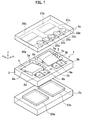
- an acceleration sensor of this embodiment has a configuration in which upper and lower surfaces of a sensor chip 1 formed of a silicon SOI substrate are sandwiched by an upper fixed plate 2a and a lower fixed plate 2b.
- the sensor chip 1 includes: a frame 3 that has two rectangular frames 3a and 3b; and two rectangular moving electrodes 4 and 5 arranged in the rectangular frames 3a and 3b in a state of being spaced apart from sidewalls of the rectangular frames 3a and 3b.
- the sensor chip 1 includes a pair of beams 6a and 6b which support the moving electrode 4 freely swingably with respect to the frame 3 by coupling substantial centers of two opposite sides on side surfaces of the moving electrode 4 to sidewalls of the rectangular frame 3a.
- the sensor chip 1 includes a pair of beams 7a and 7b which support the moving electrode 5 freely swingably with respect to the frame 3 by coupling substantial centers of two opposite sides on side surfaces of the moving electrode 5 to sidewalls of the rectangular frame 3b.
- the above-described acceleration sensor includes: detecting electrodes 8a and 8b arranged at a predetermined interval from the frame 3 and the moving electrode 4; and detecting electrodes 9a and 9b arranged at a predetermined interval from the frame 3 and the moving electrode 5. Moreover, the above-described acceleration sensor includes a grounding electrode 10 formed on a front surface of the frame 3 between the detecting electrode 8b and the detecting electrode 9a. Furthermore, the above-described detecting electrodes 8a and 8b are arranged at a predetermined interval from each other, and the above-described detecting electrodes 9a and 9b are also arranged at a predetermined interval from each other. Note that the detecting electrodes 8a and 8b and the detecting electrodes 9a and 9b are electrically connected to fixed electrodes 20a and 20b and fixed electrodes 21a and 21b, which will be described later, respectively.
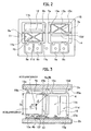
- gaps are formed between the detecting electrode 8a and the detecting electrode 8b, between the detecting electrode 9a and the detecting electrode 9b, between the detecting electrodes 8a and 8b and the frame 3, between the detecting electrodes 9a and 9b and the frame 3, between the detecting electrodes 8a and 8b and the moving electrode 4, and between the detecting electrodes 9a and 9b and the moving electrode 5.
- the respective detecting electrodes are electrically insulated from one another, and accordingly, parasitic capacitance of the respective detecting electrodes and cross talk among the detecting electrodes are reduced, thus making it possible to perform highly accurate capacity detection.
- a recessed portion 11 as a first recessed portion is formed on one side of a boundary line in the case where a straight line that connects the beams 6a and 6b to each other is taken as the boundary line.
- this recessed portion 11 is partitioned into four by a reinforcement member 16 arranged in a diagonal fashion in an inside of the recessed portion 11, and is formed as recessed portions 11a, 11b,11c and 11d.
- a recessed portion 12 is formed as a second recessed portion on the other side of the boundary line.
- recessed portions 13a, 13b, 13c and 13d are formed as a first recessed portion partitioned by a reinforcement member 16 are formed on one side of a boundary line in the case where a straight line that connects the beams 7a and 7b to each other is taken as the boundary line.
- a recessed portion 14 is formed as a second recessed portion on the other side of the boundary line.
- first recessed portion and the second recessed portion are formed separately from each other; however, the first recessed portion and the second recessed portion may be formed integrally with each other, for example, by extending the first recessed portion to the other side beyond the boundary line.
- a shape of the first recessed portion is not limited to a triangular shape shown in FIG. 2 , and may be a rectangular shape similar to that of the second recessed portion.
- a position at which the second recessed portion 12 is formed be set so that an angle made by a perpendicular line drawn down from a center of gravity O of the moving electrode 4 to a front surface 4a thereof and a straight line that connects the center of gravity O of the moving electrode 4 and the boundary line to each other can be approximately 45 degrees.
- detection sensitivities in the x-direction and the z-direction become equal to each other, and accordingly, the detection sensitivities in the respective directions can be enhanced.
- a rotation moment is increased more by forming the second recessed portion on a more distant side from the boundary line, such detection sensitivity of the acceleration sensor can be enhanced. Note that, in FIG.
- the boundary line is a straight line that connects center positions on cross sections of the beams 6a and 6b.
- the second recessed portion 12 is formed so that the center of gravity O can be located on a place where a length from the boundary line is "a" in the case where a length on the other side of the boundary line in the moving electrode 4 is defined as "2a”.
- a length on one side of the boundary line, on which the recessed portions 11b and 11d are formed is also "2a”
- a height of the moving electrode 4 is also "2a”.
- a plurality of protrusions 15a to 15g made of silicon or silicon oxide are formed on the surfaces 4a and 4b of each of the moving electrodes 4 and 5, which are opposed to the upper fixed plate 2a and the lower fixed plate 2b, as shown in FIG. 3 .
- the protrusions 15a to 15g as described above are formed, whereby each of the moving electrodes 4 and 5 does not directly collide with the upper fixed plate 2a and the lower fixed plate 2b, which are opposed thereto, even in the case where such a large acceleration that exceeds a measurement range is applied to each of the moving electrodes 4 and 5. Accordingly, breakage of the sensor chip 1 can be suppressed.
- the protrusions are formed on each of the surfaces of the moving electrodes 4 and 5, which are opposed to the upper fixed plate 2a and the lower fixed plate 2.
- similar protrusions may be formed on surfaces of the upper fixed plate 2a and the lower fixed plate 2b, which are opposed to the moving electrodes 4 and 5.
- the protrusions 15a to 15g can be formed of silicon or silicon oxide. Moreover, besides this, the protrusions 15a to 15g can be formed of a carbon material. As the carbon material as described above, a carbon nanotube can be used.
- the upper fixed plate 2a is arranged so as to be opposed to the front surface of each of the moving electrodes 4 and 5 at a predetermined interval, and further, is formed of a glass substrate. Then, on a front surface side of the upper fixed plate 2a, which is opposed to the moving electrode 4, the fixed electrodes 20a and 20b (first and second fixed electrodes) are provided on one side and other side of the boundary line, respectively in the case where the straight line that connects the centers of the beams 6a and 6b to each other is taken as the boundary line. Moreover, the fixed electrodes 20a and 20b are arranged so as to be opposed to the front surface 4a of the moving electrode 4 at a predetermined interval.
- the fixed electrodes 21a and 21b are provided on one side and other side of the boundary line, respectively in the case where the straight line that connects the centers of the beams 7a and 7b to each other is taken as the boundary line.
- the fixed electrodes 21 a and 21 b are arranged so as to be opposed to the front surface of the moving electrode 5 at a predetermined interval.
- through holes 22a to 22e are formed at positions of the upper fixed plate 2a, which are opposed to the detecting electrodes 8a, 8b, 9a and 9b and the grounding electrode 10. Outputs of the detecting electrodes 8a and 8b and the detecting electrodes 9a and 9b, which are connected to the fixed electrodes 20a and 20b and the fixed electrodes 21a and 21 b, respectively, and an output of the grounding electrode 10 are taken out through these through holes 22a to 22e.
- the lower fixed plate 2b is arranged so as to be opposed to the back surface of each of the moving electrodes 4 and 5 at a predetermined interval, and further, is formed of a glass substrate. Then, on a surface side of the lower fixed plate 2b, which is opposed to the moving electrode 4 and 5, adhesion prevention films 23a and 23b are arranged. The adhesion prevention films 23a and 23b are arranged so as to be opposed to the back surfaces 4 and 5 at a predetermined interval.
- the adhesion prevention films 23a and 23b as described above prevent the moving electrodes 4 and 5 from adhering to the lower fixed plate 2b at the time when the moving electrodes 4 and 5 are operating, and have a shock absorption effect since the moving electrodes 4 and 5 and the lower fixed plate 2b do not directly contact each other even at the time when the moving electrodes 4 and 5 undergo an excessive shock.
- the adhesion prevention films 23a and 23b can be formed of the same material as that of the fixed electrodes 20a, 20b, 21 a and 21b, and for example, can be formed of an aluminum-based alloy or the like.
- two acceleration sensors are arranged in the same chip plane, and one of the acceleration sensors is arranged so as to rotate by 180 degrees with respect to the other acceleration sensor in the chip plane, whereby an acceleration sensor structure is composed.
- two acceleration sensors are arranged adjacent to each other.
- an acceleration sensor structure according to the present invention is not limited to the embodiment as described above.
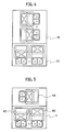
- another sensor chip 1 B is provided, which is rotated by 90 degrees in the inside of the x-y plane with respect to a sensor chip 1A similar to that of FIG. 1 , whereby a configuration may be adopted, in which acceleration in the ⁇ -direction is made detectable in addition to the accelerations in two directions which are the x-direction and the z-direction.
- three acceleration sensors may be arranged in the same chip plane, and second and third acceleration sensors (moving electrodes) 4A and 4B may be arranged so as to rotate by 90 degrees and 180 degrees, respectively with respect to a first acceleration sensor (moving electrode) 4C in the inside of the chip plane.
- An acceleration sensor structure which is constructed as described above, can detect accelerations in three axes which go along the x-direction, the ⁇ -direction and the z-direction.
- the above-described acceleration sensor performs a self-test in the following manner, and detects the accelerations in the x-direction and the z-direction, which are shown in FIG 1 .
- suction force is generated between the moving electrode 4 and the fixed electrode 20a or the fixed electrode 20b.
- suction force is generated between the moving electrode 5 and the fixed electrode 21 a or the fixed electrode 21b.
- Similar operation confirmation may be performed by generating suction force between the adhesion prevention films 23a and 23b and the moving electrodes 4 and 5.
- the moving electrodes 4 and 5 swing, whereby electrostatic capacities between the moving electrode 4 and the fixed electrodes 20a and 20b and between the moving electrode 5 and the fixed electrodes 21 a and 21 b are changed. Accordingly, it can be confirmed whether or not the acceleration sensor operates normally.
- the above-described electrostatic capacities C1 to C4 are first detected through the detecting electrodes 8a and 8b and the detecting electrodes 9a and 9b.
- the sum ( ⁇ 4 ⁇ C) of the calculated difference value CA and difference value CB is outputted as an X-output, whereby the acceleration in the x-direction, which is applied to the moving electrodes 4 and 5, can be detected from a change of an electrostatic capacity value.
- the above-described electrostatic capacities C1 to C4 are first detected through the detecting electrodes 8a and 8b and the detecting electrodes 9a and 9b.
- the sum ( ⁇ 4 ⁇ C) of the calculated difference value CA and difference value CB is outputted as a Z-output, whereby the acceleration in the z-direction, which is applied to the moving electrodes 4 and 5, can be detected from a change of an electrostatic capacity value.
- a silicon SOI substrate as shown in FIG. 6(a) which is formed of a support substrate 30a, an intermediate oxide film 30b and an active layer 30c, is prepared.
- mask layers 31 such as silicon oxide films and photoresist films are formed on both surfaces of the silicon SOI substrate, and then the mask layers 31 at positions corresponding to the moving electrodes 4 and 5 are removed.
- wet etching using a solution such as a tetramethylammonium hydride solution (TMAH) and a potassium hydride solution (KOH) or dry etching such as reactive ion etching (RIE) is performed.
- TMAH tetramethylammonium hydride solution
- KOH potassium hydride solution
- dry etching such as reactive ion etching
- silicon oxide films, carbon nanotubes and the like are adhered onto predetermined positions of bottom surfaces of the recessed portions 32a and 32b, whereby the protrusions 15 to 15g are formed. Moreover, at this time, by using a sputtering technology and an evaporation deposition technology, there are formed: a metal film 33 as the detecting electrodes 8a and 8b and the detecting electrodes 9a and 9b, which are electrically connected to the fixed electrodes; and a metal film 34 electrically connected to the metal film 33.
- the protrusions 15a to 15g are formed of the main material of the sensor chip, such as silicon and a silicon oxide film, then the protrusions 15a to 15g can be easily manufactured.
- front surfaces of the protrusions 15a to 15g may be coated with a carbon material.
- the protrusions 15a to 15g can be suppressed from being broken by collision thereof with the upper fixed plate 2a and the lower fixed plate 2b.
- the carbon nanotubes are used as the carbon material at this time, then a thickness of such coating therewith can be thinned, and accordingly, the protrusions 15a to 15g can be easily adjusted at a desired height.
- the back surface side of the silicon SOI substrate is etched in order of the support substrate 30a and the intermediate oxide film 30b, whereby, as shown in FIG. 6(d) , the moving electrodes and the first and second recessed portions are formed. Then, after the moving electrodes and the first and second recessed portions are formed, the lower fixed plate 2b in which the surface having the adhesion prevention films 23 formed thereon is defined as an opposite surface is anodically bonded to the back surface side of the silicon SOI substrate.
- the adhesion prevention films 23 are formed of the same material as that of the fixed electrodes 20a, 20b, 21 and 21b, whereby the adhesion prevention films 23 can be easily formed. Moreover, the adhesion prevention films 23 are formed at the same time of forming the fixed electrodes 20a, 20b, 21 a and 21b, whereby a distance between the fixed electrodes 20a, 20b, 21 a and 21 b and the moving electrodes 4 and 5 and a distance between the lower fixed plate 2b and the moving electrodes 4 and 5 can be accurately set.
- the adhesion prevention films 23 are deposited by such a semiconductor manufacturing process, micro irregularities are formed on front surfaces of the adhesion prevention films 23. Therefore, the moving electrodes 4 and 5 can be prevented from adhering onto the lower fixed plate 2b. Furthermore, in the case where the adhesion prevention films 23 are formed of the aluminum-based alloy, it becomes easy to process the adhesion prevention films 23 by etching, and accordingly, the adhesion prevention films 23 can be easily manufactured. Furthermore, on the front surfaces of the adhesion prevention films 23, organic material thin films, which are easy to process, and match the semiconductor manufacturing process well, are formed. Whereby short circuits between the adhesion prevention films 23 and the moving electrodes 4 and 5 may be prevented. Note that polyimide thin films can be used as the organic material thin films.
- the upper fixed plate 2a in which the through holes 22 are formed and on which the fixed electrodes 20a and 20b are formed is arranged on the silicon SOI substrate, and thereafter, the silicon SOI substrate and the upper fixed plate 2a are anodically bonded to each other. In such a way, a series of the manufacturing process in the acceleration sensor in this embodiment is completed.
- the silicon SOI substrate, the upper fixed plate 2a and the lower fixed plate 2b may be bonded to one another by resin bonding using polyimide resin and the like or eutectic bonding using gold-tin solder and the like.
- silicon substrates may be used as the upper fixed plate 2a and the lower fixed plate 2b.
- the acceleration sensor of this embodiment includes: the rectangular moving electrodes 4 and 5; the pairs of beams 6a and 6b and beams 7a and 7b, each pair of which connects to the centers of two opposite sides of a corresponding one of the moving electrodes 4 and 5, and supports the corresponding one of the moving electrodes 4 and 5 freely swingably; and the fixed electrodes 20a and 20b and the fixed electrodes 21 a and 21b, each pair of which is provided on one side of the boundary line and the other side thereof, respectively, and is arranged so as to be opposed to the front surface of the corresponding one of the moving electrodes 4 and 5.
- the straight line that connects a corresponding one of the pair of beams 6a and 6b and the pair of beams 7a and 7b to each other is taken as the boundary line.
- the recessed portions 11a, 11b, 11c and 11d (13a, 13b, 13c and 13d) and the recessed portions 12 (14) are formed on one side of the boundary line and the other side thereof, respectively.
- the acceleration sensor of this embodiment has a configuration in which upper and lower surfaces of a sensor chip 1 formed of a silicon SOI substrate are sandwiched by an upper fixed plate 2a and a lower fixed plate 2b.
- the sensor chip 1 includes: a frame 3; and two rectangular moving electrodes 4 and 5 arranged in rectangular frames 3a and 3b.
- the sensor chip 1 includes: a pair of beams 6a and 6b which support the moving electrode 4 freely swingably with respect to the frame 3; and a pair of beams 7a and 7b which support the moving electrode 5 freely swingably with respect to the frame 3.
- the above-described acceleration sensor includes: detecting electrodes 8a and 8b; and detecting electrodes 9a and 9b.
- a first recessed portion is formed on one side of a boundary line in the case where a straight line that connects the beams 6a and 6b to each other is taken as the boundary line.
- a recessed portion 12 is formed as a second recessed portion on the other side of the boundary line.
- a first recessed portion is formed on one side of a boundary line in the case where a straight line that connects the beams 7a and 7b to each other is taken as the boundary line.
- a recessed portion 14 as a second recessed portion is formed on the other side of the boundary line.
- a metal material 17 higher in specific gravity than a material for forming the moving electrodes 4 and 5 is embedded in the recessed portions 12 and 14 as the second recessed portion.
- the entire weight of the moving electrodes 4 and 5 is decreased, and accordingly, the detection sensitivity of the acceleration sensor is sometimes lowered.
- the metal material 17 higher in specific gravity than the material for forming the moving electrodes 4 and 5 is embedded in the recessed portions 12 and 14, and the weight of the moving electrodes 4 and 5 is not decreased to a large extent. Therefore, the detection sensitivities of the accelerations in the x-direction and the z-direction can be equalized to each other without lowering the detection sensitivity of the acceleration sensor.
- the moving electrodes 4 and 5 are formed of silicon
- nickel specifically gravity: 8.90 g/cm 3
- tungsten specifically gravity: 19.3 g/cm 3
- chromium specifically gravity: 7.87 g/cm 3
- palladium specifically gravity: 12.02 g/cm 3
- platinum specifically gravity: 21.45 g/cm 3
- manganese specifically gravity: 7.43 g/cm 3
- weight of the metal material 17 be substantially equal to weight of a reinforcement member 16 that is formed in an inside of the first recessed portion 11 and composes an outer wall of the first recessed portion 11.
- the weight of the metal material 17 is equalized to that of the reinforcement member 16, whereby a size of the moving electrodes 4 and 5 can be miniaturized without decreasing the entire weight of the moving electrodes 4 and 5, and an acceleration sensor with higher sensitivity and higher precision can be obtained.
- a position at which the second recessed portion 12 having the metal material 17 filled therein is formed be set so that an angle made by a perpendicular line drawn down from a center of gravity O of the moving electrode 4 to a front surface 4a thereof and a straight line that connects the center of gravity O of the moving electrode 4 and the boundary line to each other can be approximately 45 degrees.
- the detection sensitivities in the x-direction and the z-direction become equal to each other, and accordingly, the detection sensitivities in the respective directions can be enhanced.
- a silicon SOI substrate as shown in FIG. 8(a) which is formed of a support substrate 30a, an intermediate oxide film 30b and an active layer 30c, is prepared.
- mask layers 31 are formed on both surfaces of the silicon SOI substrate, and the mask layers 31 at positions corresponding to the moving electrodes 4 and 5 are removed.
- the above-described wet etching or dry etching is performed.
- recessed portions 32a and 32b for allowing displacement of the moving electrodes 4 and 5 are formed on a front surface side and back surface side of the silicon SOI substrate.
- protrusions 15a to 15g there are formed: protrusions 15a to 15g; a metal film 33 as the detecting electrodes 8a and 8b and the detecting electrodes 9a and 9b; and a metal film 34 electrically connected to the metal film 33.
- the back surface side of the silicon SOI substrate is etched in order of the support substrate 30a and the intermediate oxide film 30b, whereby, as shown in FIG. 8(d) , the moving electrodes and the first and second recessed portions are formed. Moreover, the metal material 17 is embedded in the second recessed portion. Then, the lower fixed plate 2b in which the surface having the adhesion prevention films 23 formed thereon is defined as an opposite surface is anodically bonded to the back surface side of the silicon SOI substrate.
- the upper fixed plate 2a in which through holes are formed and on which fixed electrodes are formed is arranged on the silicon SOI substrate, and thereafter, the silicon SOI substrate and the upper fixed plate 2a are anodically bonded to each other. In such a way, a series of the manufacturing process in the acceleration sensor in this embodiment is completed.
- the metal material 17 higher in specific gravity than the material for forming the moving electrodes 4 and 5 is embedded in the recessed portions 12 and 14 as the second recessed portion.
- the detection sensitivities of the accelerations in the x-direction and the z-direction can be equalized to each other, and further, the weight of the moving electrodes 4 and 5 is not decreased to a large extent, and accordingly, the acceleration sensor with higher sensitivity and higher precision can be provided.
- the recessed portions are formed also on the other side as well as on one side of the back surface of the moving electrode in which the straight line that connects the pair of beams to each other is taken as the boundary line, whereby the detection sensitivity is adjusted between two directions. Therefore, the detection sensitivity can be equalized between two directions without requiring a long manufacturing time.
Landscapes
- Physics & Mathematics (AREA)
- General Physics & Mathematics (AREA)
- Pressure Sensors (AREA)
Description
- The present invention relates to an acceleration sensor that detects an acceleration, which is applied to a moving electrode, by detecting a change of an electrostatic capacity between the moving electrode and a fixed electrode, the change following a swing of the moving electrode.
- Heretofore, an acceleration sensor has been known, which includes: a rectangular weight portion that has a moving electrode; beams which support the weight portion freely swingably; and first and second fixed electrodes arranged so as to be opposed to the weight portion (for example, refer to Patent Literature 1). In the acceleration sensor as described above, a recessed portion is formed on the weight portion so that a rotation moment, in which a straight line (beam axis) that connects a pair of the beams to each other is used as a rotation axis, can be generated when acceleration is applied to the acceleration sensor. In such a way, one side and the other side in the weight portion, which are defined by the beam axis taken as a boundary line, are differentiated from each other in terms of weight.
- Patent Literature 1: Specification of United States Patent Application Publication No.
2007/0000323 - Here, in the case where the recessed portion is formed only on one side in the weight portion, which is defined by the beam axis taken as the boundary line, the moving electrode on one side becomes prone to be affected by distortion. As a result, the moving electrode is deformed, and it becomes difficult to precisely control a distance between the moving electrode and the fixed electrodes. From a background as described above, in the acceleration sensor described in
Patent Literature 1, such deformation of the moving electrode is suppressed by providing a reinforcement member on the recessed portion. However, in the case of providing the reinforcement member on the recessed portion, at the time of detecting the accelerations in two directions which are the x-direction and the z-direction, a difference occurs in detection sensitivity between the two directions. Therefore, in the acceleration sensor described inPatent Literature 1, the detection sensitivity is equalized between the two directions by thickening a thickness of the weight portion. However, in the case of thickening the thickness of the weight portion, a long manufacturing time (etching time) is required for forming the recessed portion. - The present invention has been made in consideration of the problems as described above, which are inherent in the conventional technology. Then, it is an object of the present invention to provide an acceleration sensor capable of equalizing the detection sensitivity between the two directions without requiring a long manufacturing time.
- An acceleration sensor according to an aspect of the present invention includes: a rectangular moving electrode; a pair of beams which connect to centers of two opposite sides of the moving electrode, and support the moving electrode freely swingably; and first and second fixed electrodes which are provided on one side and other side of a boundary line, respectively, and are arranged to be opposed to a front surface of the moving electrode at a predetermined interval, wherein a straight line that connects the pair of beams to each other is taken as the boundary line. Then, on a back surface of the moving electrode, first and second recessed portions are formed on one side of the boundary line and the other side thereof, respectively.
-
- [
Fig. 1] FIG. 1 is an exploded perspective view showing a configuration of an acceleration sensor according to a first embodiment of the present invention. - [
Fig. 2] FIG. 2 is a lower surface view showing a sensor chip in the acceleration sensor. - [
Fig. 3] FIG. 3 is a partial cross-sectional view of the acceleration sensor. - [
Fig. 4] FIG. 4 is a schematic view showing an example of an acceleration sensor structure including a plurality of the acceleration sensors according to the first embodiment. - [
Fig. 5] FIG. 5 is a schematic view showing another example of the acceleration sensor structure including the plurality of the acceleration sensors according to the first embodiment. - [
Fig. 6] FIG. 6 is a schematic view showing a manufacturing process of the acceleration sensor according to the first embodiment. - [
Fig. 7] FIG. 7 is a partial cross-sectional view showing a configuration of an acceleration sensor according to a second embodiment of the present invention. - [
Fig. 8] FIG. 8 is a schematic view showing a manufacturing process of the acceleration sensor according to the second embodiment. - A description is first made in detail of an acceleration sensor of a first embodiment based on the drawings.
- As shown in
FIG. 1 , an acceleration sensor of this embodiment has a configuration in which upper and lower surfaces of asensor chip 1 formed of a silicon SOI substrate are sandwiched by an upperfixed plate 2a and a lowerfixed plate 2b. Thesensor chip 1 includes: aframe 3 that has tworectangular frames electrodes rectangular frames rectangular frames sensor chip 1 includes a pair ofbeams electrode 4 freely swingably with respect to theframe 3 by coupling substantial centers of two opposite sides on side surfaces of the movingelectrode 4 to sidewalls of therectangular frame 3a. Furthermore, thesensor chip 1 includes a pair ofbeams electrode 5 freely swingably with respect to theframe 3 by coupling substantial centers of two opposite sides on side surfaces of the movingelectrode 5 to sidewalls of therectangular frame 3b. - The above-described acceleration sensor includes: detecting
electrodes frame 3 and the movingelectrode 4; and detectingelectrodes frame 3 and the movingelectrode 5. Moreover, the above-described acceleration sensor includes agrounding electrode 10 formed on a front surface of theframe 3 between the detectingelectrode 8b and the detectingelectrode 9a. Furthermore, the above-described detectingelectrodes electrodes electrodes electrodes electrodes electrodes - In this embodiment, as shown in
FIG. 2 , gaps are formed between the detectingelectrode 8a and the detectingelectrode 8b, between the detectingelectrode 9a and the detectingelectrode 9b, between the detectingelectrodes frame 3, between the detectingelectrodes frame 3, between the detectingelectrodes electrode 4, and between the detectingelectrodes electrode 5. With such a configuration, the respective detecting electrodes are electrically insulated from one another, and accordingly, parasitic capacitance of the respective detecting electrodes and cross talk among the detecting electrodes are reduced, thus making it possible to perform highly accurate capacity detection. - Then as shown in
FIG. 2 , on a back surface of the movingelectrode 4, arecessed portion 11 as a first recessed portion is formed on one side of a boundary line in the case where a straight line that connects thebeams recessed portion 11 is partitioned into four by areinforcement member 16 arranged in a diagonal fashion in an inside of therecessed portion 11, and is formed as recessedportions electrode 4, arecessed portion 12 is formed as a second recessed portion on the other side of the boundary line. In a similar way, on a back surface of the movingelectrode 5, recessedportions reinforcement member 16 are formed on one side of a boundary line in the case where a straight line that connects thebeams electrode 5, arecessed portion 14 is formed as a second recessed portion on the other side of the boundary line. - In this embodiment, the first recessed portion and the second recessed portion are formed separately from each other; however, the first recessed portion and the second recessed portion may be formed integrally with each other, for example, by extending the first recessed portion to the other side beyond the boundary line. Moreover, a shape of the first recessed portion is not limited to a triangular shape shown in
FIG. 2 , and may be a rectangular shape similar to that of the second recessed portion. - Here, as shown in
FIG. 3 , it is preferable that a position at which the secondrecessed portion 12 is formed be set so that an angle made by a perpendicular line drawn down from a center of gravity O of the movingelectrode 4 to afront surface 4a thereof and a straight line that connects the center of gravity O of the movingelectrode 4 and the boundary line to each other can be approximately 45 degrees. In such a way, detection sensitivities in the x-direction and the z-direction become equal to each other, and accordingly, the detection sensitivities in the respective directions can be enhanced. However, since a rotation moment is increased more by forming the second recessed portion on a more distant side from the boundary line, such detection sensitivity of the acceleration sensor can be enhanced. Note that, inFIG. 3 , the boundary line is a straight line that connects center positions on cross sections of thebeams FIG. 3 , the secondrecessed portion 12 is formed so that the center of gravity O can be located on a place where a length from the boundary line is "a" in the case where a length on the other side of the boundary line in the movingelectrode 4 is defined as "2a". Note that, in the acceleration sensor ofFIG. 3 , in themoving electrode 4, a length on one side of the boundary line, on which therecessed portions electrode 4 is also "2a". - On the
surfaces electrodes fixed plate 2a and the lowerfixed plate 2b, as shown inFIG. 3 , a plurality ofprotrusions 15a to 15g made of silicon or silicon oxide are formed. Theprotrusions 15a to 15g as described above are formed, whereby each of the movingelectrodes fixed plate 2a and the lowerfixed plate 2b, which are opposed thereto, even in the case where such a large acceleration that exceeds a measurement range is applied to each of the movingelectrodes sensor chip 1 can be suppressed. Note that, in this embodiment, the protrusions are formed on each of the surfaces of the movingelectrodes fixed plate 2a and the lower fixed plate 2. However, similar protrusions may be formed on surfaces of the upperfixed plate 2a and the lowerfixed plate 2b, which are opposed to the movingelectrodes - As mentioned above, the
protrusions 15a to 15g can be formed of silicon or silicon oxide. Moreover, besides this, theprotrusions 15a to 15g can be formed of a carbon material. As the carbon material as described above, a carbon nanotube can be used. - As shown in
FIG. 3 , the upperfixed plate 2a is arranged so as to be opposed to the front surface of each of the movingelectrodes fixed plate 2a, which is opposed to the movingelectrode 4, thefixed electrodes beams fixed electrodes front surface 4a of the movingelectrode 4 at a predetermined interval. Furthermore, in a similar way, on a front surface side of the fixedplate 2a, which is opposed to the movingelectrode 5, the fixedelectrodes beams electrodes electrodes electrode 5 at a predetermined interval. - Moreover, as shown in
FIG. 1 , throughholes 22a to 22e are formed at positions of the upper fixedplate 2a, which are opposed to the detectingelectrodes electrode 10. Outputs of the detectingelectrodes electrodes electrodes electrodes electrode 10 are taken out through these throughholes 22a to 22e. - Moreover, as shown in
FIG. 3 , the lower fixedplate 2b is arranged so as to be opposed to the back surface of each of the movingelectrodes plate 2b, which is opposed to the movingelectrode adhesion prevention films adhesion prevention films back surfaces adhesion prevention films electrodes plate 2b at the time when the movingelectrodes electrodes plate 2b do not directly contact each other even at the time when the movingelectrodes adhesion prevention films electrodes - In the embodiment of
FIG. 1 andFIG. 2 , two acceleration sensors are arranged in the same chip plane, and one of the acceleration sensors is arranged so as to rotate by 180 degrees with respect to the other acceleration sensor in the chip plane, whereby an acceleration sensor structure is composed. Moreover, in the embodiment ofFIG. 1 andFIG. 2 , two acceleration sensors are arranged adjacent to each other. However, an acceleration sensor structure according to the present invention is not limited to the embodiment as described above. For example, as shown inFIG. 4 , anothersensor chip 1 B is provided, which is rotated by 90 degrees in the inside of the x-y plane with respect to asensor chip 1A similar to that ofFIG. 1 , whereby a configuration may be adopted, in which acceleration in the γ-direction is made detectable in addition to the accelerations in two directions which are the x-direction and the z-direction. - Moreover, as shown in
FIG. 5 , three acceleration sensors may be arranged in the same chip plane, and second and third acceleration sensors (moving electrodes) 4A and 4B may be arranged so as to rotate by 90 degrees and 180 degrees, respectively with respect to a first acceleration sensor (moving electrode) 4C in the inside of the chip plane. An acceleration sensor structure, which is constructed as described above, can detect accelerations in three axes which go along the x-direction, the γ-direction and the z-direction. - The above-described acceleration sensor performs a self-test in the following manner, and detects the accelerations in the x-direction and the z-direction, which are shown in
FIG 1 . - In the case of operating the moving
electrode 4, suction force is generated between the movingelectrode 4 and the fixedelectrode 20a or the fixedelectrode 20b. In a similar way, in the case of operating the movingelectrode 5, suction force is generated between the movingelectrode 5 and the fixedelectrode 21 a or the fixedelectrode 21b. Similar operation confirmation may be performed by generating suction force between theadhesion prevention films electrodes electrodes electrode 4 and the fixedelectrodes electrode 5 and the fixedelectrodes - In the case where the acceleration in the x-direction is applied to the moving
electrode 4, the electrostatic capacities C1 and C2 between the movingelectrode 4 and the fixedelectrodes electrode 4 and the fixedelectrodes electrode 4.

- Moreover, in a similar way, in the case where the acceleration in the x-direction is applied to the moving
electrode 5, the electrostatic capacities C3 and C4 between the movingelectrode 5 and the fixedelectrodes electrode 5 and the fixedelectrodes electrode 5.

- Then, the above-described electrostatic capacities C1 to C4 are first detected through the detecting
electrodes electrodes electrodes - In the case where the acceleration in the z-direction is applied to the moving
electrode 4, the electrostatic capacities C1 and C2 between the movingelectrode 4 and the fixedelectrodes electrode 4 and the fixedelectrodes electrode 4.

- Moreover, in a similar way, in the case where the acceleration in the z-direction is applied to the moving
electrode 5, the electrostatic capacities C3 and C4 between the movingelectrode 5 and the fixedelectrodes electrode 5 and the fixedelectrodes electrode 5.

- Then, the above-described electrostatic capacities C1 to C4 are first detected through the detecting
electrodes electrodes electrodes - Next, a description is made of a manufacturing method of the acceleration sensor of this embodiment with reference to
FIGS. 6(a) to 6(e) . - In this embodiment, first, a silicon SOI substrate as shown in
FIG. 6(a) , which is formed of asupport substrate 30a, anintermediate oxide film 30b and anactive layer 30c, is prepared. Next, mask layers 31 such as silicon oxide films and photoresist films are formed on both surfaces of the silicon SOI substrate, and then the mask layers 31 at positions corresponding to the movingelectrodes FIG. 6(b) , recessedportions electrodes - Next, as shown in
FIG. 6(c) , silicon oxide films, carbon nanotubes and the like are adhered onto predetermined positions of bottom surfaces of the recessedportions metal film 33 as the detectingelectrodes electrodes metal film 34 electrically connected to themetal film 33. - Here, in the case where the
protrusions 15a to 15g are formed of the main material of the sensor chip, such as silicon and a silicon oxide film, then theprotrusions 15a to 15g can be easily manufactured. Note that front surfaces of theprotrusions 15a to 15g may be coated with a carbon material. With such a configuration, mechanical strength of theprotrusions 15a to 15g is increased, and theprotrusions 15a to 15g can be suppressed from being broken by collision thereof with the upper fixedplate 2a and the lower fixedplate 2b. Moreover, if the carbon nanotubes are used as the carbon material at this time, then a thickness of such coating therewith can be thinned, and accordingly, theprotrusions 15a to 15g can be easily adjusted at a desired height. - Next, the back surface side of the silicon SOI substrate is etched in order of the
support substrate 30a and theintermediate oxide film 30b, whereby, as shown inFIG. 6(d) , the moving electrodes and the first and second recessed portions are formed. Then, after the moving electrodes and the first and second recessed portions are formed, the lower fixedplate 2b in which the surface having theadhesion prevention films 23 formed thereon is defined as an opposite surface is anodically bonded to the back surface side of the silicon SOI substrate. - Note that the
adhesion prevention films 23 are formed of the same material as that of the fixedelectrodes adhesion prevention films 23 can be easily formed. Moreover, theadhesion prevention films 23 are formed at the same time of forming the fixedelectrodes fixed electrodes electrodes plate 2b and the movingelectrodes - Moreover, in the case where the
adhesion prevention films 23 are deposited by such a semiconductor manufacturing process, micro irregularities are formed on front surfaces of theadhesion prevention films 23. Therefore, the movingelectrodes plate 2b. Furthermore, in the case where theadhesion prevention films 23 are formed of the aluminum-based alloy, it becomes easy to process theadhesion prevention films 23 by etching, and accordingly, theadhesion prevention films 23 can be easily manufactured. Furthermore, on the front surfaces of theadhesion prevention films 23, organic material thin films, which are easy to process, and match the semiconductor manufacturing process well, are formed. Whereby short circuits between theadhesion prevention films 23 and the movingelectrodes - Next, as shown in
FIG. 6(e) , the upper fixedplate 2a in which the throughholes 22 are formed and on which the fixedelectrodes plate 2a are anodically bonded to each other. In such a way, a series of the manufacturing process in the acceleration sensor in this embodiment is completed. - Note that the silicon SOI substrate, the upper fixed
plate 2a and the lower fixedplate 2b may be bonded to one another by resin bonding using polyimide resin and the like or eutectic bonding using gold-tin solder and the like. Moreover, silicon substrates may be used as the upper fixedplate 2a and the lower fixedplate 2b. However, in the case where the silicon substrates are used as the upper fixedplate 2a and the lower fixedplate 2b, it is desirable to form an insulating film between the fixed electrodes and the upper fixedplate 2a so that the fixed electrodes and the upper fixedplate 2a can be electrically insulated from each other. - As obvious from the above description, the acceleration sensor of this embodiment includes: the rectangular moving
electrodes beams beams electrodes electrodes electrodes electrodes electrodes beams beams electrodes portions electrodes - Next, a description is made in detail of an acceleration sensor of a second embodiment based on the drawings. Note that the same reference numerals are assigned to the same components as those in the first embodiment, and a duplicate description is omitted.
- In a similar way to the first embodiment, the acceleration sensor of this embodiment has a configuration in which upper and lower surfaces of a
sensor chip 1 formed of a silicon SOI substrate are sandwiched by an upper fixedplate 2a and a lower fixedplate 2b. Thesensor chip 1 includes: aframe 3; and two rectangular movingelectrodes rectangular frames sensor chip 1 includes: a pair ofbeams electrode 4 freely swingably with respect to theframe 3; and a pair ofbeams electrode 5 freely swingably with respect to theframe 3. Furthermore, the above-described acceleration sensor includes: detectingelectrodes electrodes - Moreover, in a similar way to the first embodiment, in the acceleration sensor of this embodiment, on a back surface of the moving
electrode 4, a first recessed portion is formed on one side of a boundary line in the case where a straight line that connects thebeams electrode 4, a recessedportion 12 is formed as a second recessed portion on the other side of the boundary line. In a similar way, on a back surface of the movingelectrode 5, a first recessed portion is formed on one side of a boundary line in the case where a straight line that connects thebeams electrode 5, a recessedportion 14 as a second recessed portion is formed on the other side of the boundary line. - Then, in this embodiment, as shown in
FIG. 7 , ametal material 17 higher in specific gravity than a material for forming the movingelectrodes portions portions electrodes electrodes metal material 17 higher in specific gravity than the material for forming the movingelectrodes portions electrodes - Here, in the case where the moving
electrodes metal material 17, nickel (specific gravity: 8.90 g/cm3), tungsten (specific gravity: 19.3 g/cm3), chromium (specific gravity: 7.87 g/cm3), palladium (specific gravity: 12.02 g/cm3), platinum (specific gravity: 21.45 g/cm3) and manganese (specific gravity: 7.43 g/cm3) can be illustrated since the specific gravity of silicon is 2.33 g/cm3. - Moreover, it is desirable that weight of the
metal material 17 be substantially equal to weight of areinforcement member 16 that is formed in an inside of the first recessedportion 11 and composes an outer wall of the first recessedportion 11. The weight of themetal material 17 is equalized to that of thereinforcement member 16, whereby a size of the movingelectrodes electrodes - Here, in a similar way to the first embodiment, it is preferable that a position at which the second recessed
portion 12 having themetal material 17 filled therein is formed be set so that an angle made by a perpendicular line drawn down from a center of gravity O of the movingelectrode 4 to afront surface 4a thereof and a straight line that connects the center of gravity O of the movingelectrode 4 and the boundary line to each other can be approximately 45 degrees. In such a way, the detection sensitivities in the x-direction and the z-direction become equal to each other, and accordingly, the detection sensitivities in the respective directions can be enhanced. - Next, a description is made of a manufacturing method of the acceleration sensor of this embodiment with reference to
FIG. 8 . - In this embodiment, first, a silicon SOI substrate as shown in
FIG. 8(a) , which is formed of asupport substrate 30a, anintermediate oxide film 30b and anactive layer 30c, is prepared. Next, in a similar way to the first embodiment, mask layers 31 are formed on both surfaces of the silicon SOI substrate, and the mask layers 31 at positions corresponding to the movingelectrodes FIG. 8(b) , recessedportions electrodes - Next, as shown in
FIG. 8(c) , in a similar way to the first embodiment, there are formed:protrusions 15a to 15g; ametal film 33 as the detectingelectrodes electrodes metal film 34 electrically connected to themetal film 33. - Next, the back surface side of the silicon SOI substrate is etched in order of the
support substrate 30a and theintermediate oxide film 30b, whereby, as shown inFIG. 8(d) , the moving electrodes and the first and second recessed portions are formed. Moreover, themetal material 17 is embedded in the second recessed portion. Then, the lower fixedplate 2b in which the surface having theadhesion prevention films 23 formed thereon is defined as an opposite surface is anodically bonded to the back surface side of the silicon SOI substrate. - Next, as shown in
FIG. 8(e) , the upper fixedplate 2a in which through holes are formed and on which fixed electrodes are formed is arranged on the silicon SOI substrate, and thereafter, the silicon SOI substrate and the upper fixedplate 2a are anodically bonded to each other. In such a way, a series of the manufacturing process in the acceleration sensor in this embodiment is completed. - As described above, in the acceleration sensor of this embodiment, the
metal material 17 higher in specific gravity than the material for forming the movingelectrodes portions electrodes - The entire contents of Japanese Patent Application No.
2008-299989 (filed on November 25, 2008 2008-300004 (filed on November 25, 2008 - The description has been made above of the contents of the present invention along the embodiments and the examples. However, it is obvious for those skilled in the art that the present invention is not limited to the description of these, and is modifiable and improvable in various ways.
- In accordance with the acceleration sensor of the present invention, the recessed portions are formed also on the other side as well as on one side of the back surface of the moving electrode in which the straight line that connects the pair of beams to each other is taken as the boundary line, whereby the detection sensitivity is adjusted between two directions. Therefore, the detection sensitivity can be equalized between two directions without requiring a long manufacturing time.
-
- 2a: Upper fixed plate
- 2b: Lower fixed plate
- 3: Frame
- 4, 5: Moving electrode
- 6a, 6b, 7a, 7b: Beam
- 8a, 8b, 9a, 9b: Detecting electrode
- 11, 13: First recessed portion
- 12, 14: Second recessed portion
- 15a, 15b, 15c, 15d, 15e, 15f, 15g: Protrusion
- 16: Reinforcement member
- 17: Metal material
- 23a, 23b: Adhesion prevention film
Claims (15)
- An acceleration sensor comprising:a rectangular moving electrode (4, 5);a pair of beams (6a, 6b, 7a, 7b) which connect to centers of two opposite sides of the moving electrode (4, 5), and support the moving electrode (4, 5) freely swingably; andfirst and second fixed electrodes (20a, 20b, 21 a, 21 b) which are provided on one side and other side of a boundary line, respectively, and are arranged to be opposed to a front surface of the moving electrode (4, 5) at a predetermined interval, wherein a straight line that connects the pair of beams (6a, 6b, 7a, 7b) to each other is taken as the boundary line,wherein, on a back surface of the moving electrode (4, 5), first and second recessed portions (11, 12, 13, 14) are formed on one side of the boundary line and the other side thereof, respectively.
- The acceleration sensor according to claim 1, wherein the acceleration sensor detects acceleration in a first direction, which is applied to the moving electrode (4, 5), and acceleration in a second direction, which is applied to the moving electrode (4, 5) and is orthogonal to the acceleration in the first direction.
- The acceleration sensor according to claim 1 or 2, further comprising:a frame (3) that incorporates the moving electrode(4, 5) therein; andfirst and second detecting electrodes (8a, 8b, 9a, 9b) formed in the frame (3) and electrically connected to the first and second fixed electrodes (20a, 20b, 21a, 21 b), respectively,wherein gaps are formed between the first detecting electrode and the second detecting electrode, between the first and second detecting electrodes (8a, 8b, 9a, 9b) and the frame (3), and between the first and second detecting electrodes (8a, 8b, 9a, 9b) and the moving electrode (4, 5).
- The acceleration sensor according to any one of claims 1 to 3, further comprising:protrusions (15a, 15b, 15c, 15d) formed on opposite surfaces of the first and second fixed electrodes (20a, 20b, 21a, 21b) to the moving electrode (4, 5) or on an opposite surface of the moving electrode (4, 5) to the first and second fixed electrodes (20a, 20b, 21 a, 21 b).
- The acceleration sensor according to claim 4, wherein the protrusions (15a, 15b, 15c, 15d) are formed of silicon, silicon oxide or a carbon material.
- The acceleration sensor according to any one of claims 1 to 5, further comprising:a fixed plate (2b) arranged to be opposed to the back surface of the moving electrode (4, 5) at a predetermined interval,wherein an adhesion prevention film (23a, 23b), which prevents adhesion between the moving electrode (4, 5) and the fixed plate, is formed on a surface of the fixed plate (2b), and the surface is opposed to the moving electrode (4, 5).
- The acceleration sensor according to claim 6, wherein the adhesion prevention film (23a, 23b) is formed of a same material as that of the first and second fixed electrodes (20a, 20b, 21 a, 21 b).
- The acceleration sensor according to claim 6 or 7, wherein an organic material thin film is formed on a front surface of the adhesion prevention film (23a, 23b).
- The acceleration sensor according to any one of claims 1 to 8, wherein an angle made by a perpendicular line drawn down from a center of gravity of the moving electrode (4, 5) to the front surface thereof and a straight line that connects the center of gravity of the moving electrode (4, 5) and the boundary line to each other is approximately 45 degrees.
- The acceleration sensor according to any one of claims 1 to 9, wherein a metal material (17) is embedded in the second recessed portion (12, 14).
- The acceleration sensor according to claim 10, wherein the metal material (17) is formed of a metal material having specific gravity equal to or larger than specific gravity of a material for forming the moving electrode (4, 5).
- The acceleration sensor according to claim 10 or 11, wherein weight of the metal material (17) is substantially equal to weight of a reinforcement member (16) that constructs an outer wall of the first recessed portion (11, 13).
- An acceleration sensor structure comprising:a plurality of the acceleration sensors, each acceleration sensor according to any one of claims 1 to 12,wherein the acceleration sensors are formed in a same chip plane.
- The acceleration sensor structure according to claim 13, wherein two of the acceleration sensors are arranged in the same chip plane, and
one of the acceleration sensors is arranged to rotate by 180 degrees with respect to the other acceleration sensor in the chip plane. - The acceleration sensor structure according to claim 13, wherein three of the acceleration sensors are arranged in the same chip plane, and
second and third acceleration sensors are arranged to rotate by 90 degrees and 180 degrees, respectively with respect to a first acceleration sensor in the chip plane.
Applications Claiming Priority (3)
| Application Number | Priority Date | Filing Date | Title |
|---|---|---|---|
| JP2008299989A JP4965546B2 (en) | 2008-11-25 | 2008-11-25 | Acceleration sensor |
| JP2008300004A JP4965547B2 (en) | 2008-11-25 | 2008-11-25 | Acceleration sensor |
| PCT/JP2009/069631 WO2010061777A1 (en) | 2008-11-25 | 2009-11-19 | Acceleration sensor |
Publications (3)
| Publication Number | Publication Date |
|---|---|
| EP2352037A1 EP2352037A1 (en) | 2011-08-03 |
| EP2352037A4 EP2352037A4 (en) | 2012-06-06 |
| EP2352037B1 true EP2352037B1 (en) | 2013-07-10 |
Family
ID=42225653
Family Applications (1)
| Application Number | Title | Priority Date | Filing Date |
|---|---|---|---|
| EP09829025.7A Not-in-force EP2352037B1 (en) | 2008-11-25 | 2009-11-19 | Acceleration sensor |
Country Status (4)
| Country | Link |
|---|---|
| US (1) | US8850889B2 (en) |
| EP (1) | EP2352037B1 (en) |
| CN (1) | CN102124352B (en) |
| WO (1) | WO2010061777A1 (en) |
Families Citing this family (7)
| Publication number | Priority date | Publication date | Assignee | Title |
|---|---|---|---|---|
| WO2011064642A2 (en) | 2009-11-24 | 2011-06-03 | パナソニック電工株式会社 | Acceleration sensor |
| JP2011112392A (en) * | 2009-11-24 | 2011-06-09 | Panasonic Electric Works Co Ltd | Acceleration sensor |
| CN102156203B (en) * | 2011-03-15 | 2013-07-24 | 迈尔森电子(天津)有限公司 | MEMS (micro-electromechanical system) inertial sensor and forming method of MEMS inertial sensor |
| JP6206650B2 (en) | 2013-07-17 | 2017-10-04 | セイコーエプソン株式会社 | Functional element, electronic device, and moving object |
| JP6146566B2 (en) * | 2013-08-06 | 2017-06-14 | セイコーエプソン株式会社 | Physical quantity sensors, electronic devices, and moving objects |
| CN104459203B (en) * | 2014-12-25 | 2017-08-25 | 歌尔股份有限公司 | Z axis structure and three axis accelerometer in a kind of accelerometer |
| US11307218B2 (en) * | 2020-05-22 | 2022-04-19 | Invensense, Inc. | Real-time isolation of self-test and linear acceleration signals |
Family Cites Families (14)
| Publication number | Priority date | Publication date | Assignee | Title |
|---|---|---|---|---|
| FR2617607B1 (en) | 1987-06-30 | 1989-12-01 | Applic Gles Electrici Meca | PENDULUM RE-BALANCING ACCELEROMETER AND METHOD FOR MANUFACTURING SUCH AN ACCELEROMETER |
| JPS6459161A (en) | 1987-08-31 | 1989-03-06 | Fujikura Ltd | Semiconductor acceleration sensor and manufacture thereof |
| AU4722097A (en) | 1997-02-21 | 1998-09-09 | Matsushita Electric Works Ltd. | Acceleration sensor element and method of its manufacture |
| JP2000187041A (en) | 1998-12-24 | 2000-07-04 | Mitsubishi Electric Corp | Capacitive acceleration sensor and method of manufacturing the same |
| JP4174979B2 (en) | 2001-07-13 | 2008-11-05 | 松下電工株式会社 | Acceleration sensor |
| EP1491901A1 (en) | 2003-06-25 | 2004-12-29 | Matsushita Electric Works, Ltd. | Semiconductor acceleration sensor and method of manufacturing the same |
| US7367232B2 (en) * | 2004-01-24 | 2008-05-06 | Vladimir Vaganov | System and method for a three-axis MEMS accelerometer |
| US7121141B2 (en) | 2005-01-28 | 2006-10-17 | Freescale Semiconductor, Inc. | Z-axis accelerometer with at least two gap sizes and travel stops disposed outside an active capacitor area |
| JP2006214743A (en) | 2005-02-01 | 2006-08-17 | Matsushita Electric Works Ltd | Semiconductor acceleration sensor |
| FI119299B (en) | 2005-06-17 | 2008-09-30 | Vti Technologies Oy | Process for manufacturing capacitive acceleration sensor and capacitive acceleration sensor |
| JP2007298405A (en) | 2006-04-28 | 2007-11-15 | Matsushita Electric Works Ltd | Electrostatic capacity type sensor |
| EP2023152A4 (en) * | 2006-04-28 | 2011-11-02 | Panasonic Elec Works Co Ltd | CAPACITOR SENSOR |
| JP2008300004A (en) | 2007-06-01 | 2008-12-11 | Toshiba Alpine Automotive Technology Corp | Optical disc apparatus and control method thereof |
| JP5458232B2 (en) | 2007-06-01 | 2014-04-02 | ピーエスフォー ルクスコ エスエイアールエル | Antifuse replacement determination circuit and antifuse replacement determination method for semiconductor memory device |
-
2009
- 2009-11-19 WO PCT/JP2009/069631 patent/WO2010061777A1/en not_active Ceased
- 2009-11-19 US US13/058,923 patent/US8850889B2/en not_active Expired - Fee Related
- 2009-11-19 CN CN2009801315608A patent/CN102124352B/en not_active Expired - Fee Related
- 2009-11-19 EP EP09829025.7A patent/EP2352037B1/en not_active Not-in-force
Also Published As
| Publication number | Publication date |
|---|---|
| US20110138914A1 (en) | 2011-06-16 |
| EP2352037A1 (en) | 2011-08-03 |
| EP2352037A4 (en) | 2012-06-06 |
| US8850889B2 (en) | 2014-10-07 |
| CN102124352A (en) | 2011-07-13 |
| WO2010061777A1 (en) | 2010-06-03 |
| CN102124352B (en) | 2013-04-17 |
Similar Documents
| Publication | Publication Date | Title |
|---|---|---|
| CN102667497B (en) | Acceleration sensor | |
| EP2352037A1 (en) | Acceleration sensor | |
| US9134189B2 (en) | Dynamic quantity sensor and dynamic quantity sensor system | |
| EP2246706B1 (en) | Physical quantity sensor | |
| CN102654409A (en) | Capacitive sensor | |
| CN113624991A (en) | A Z-axis accelerometer | |
| US9274153B2 (en) | Electrostatic capacitance sensor | |
| EP2506017B1 (en) | Acceleration sensor | |
| JP4965546B2 (en) | Acceleration sensor | |
| JP2001004658A (en) | Dual-shaft semiconductor acceleration sensor and manufacture thereof | |
| JP4965547B2 (en) | Acceleration sensor | |
| JP5716149B2 (en) | Acceleration sensor | |
| JP5535124B2 (en) | Acceleration sensor | |
| CN216595182U (en) | Z-axis accelerometer | |
| JP4775412B2 (en) | Semiconductor physical quantity sensor | |
| JP5657929B2 (en) | Acceleration sensor | |
| JP2010107240A (en) | Monoaxial acceleration sensor and triaxial acceleration sensor using the same | |
| JP2012220376A (en) | Acceleration sensor | |
| JP4752874B2 (en) | Semiconductor physical quantity sensor | |
| JP2012008022A (en) | Acceleration sensor | |
| JP2011112392A (en) | Acceleration sensor | |
| JP2010210432A (en) | Method of manufacturing acceleration sensor, and acceleration sensor manufactured by the method | |
| JP2010210422A (en) | Acceleration sensor | |
| JP2010210416A (en) | Acceleration sensor | |
| JP2012047530A (en) | Electrostatic capacitance type sensor |
Legal Events
| Date | Code | Title | Description |
|---|---|---|---|
| PUAI | Public reference made under article 153(3) epc to a published international application that has entered the european phase |
Free format text: ORIGINAL CODE: 0009012 |
|
| 17P | Request for examination filed |
Effective date: 20110216 |
|
| AK | Designated contracting states |
Kind code of ref document: A1 Designated state(s): AT BE BG CH CY CZ DE DK EE ES FI FR GB GR HR HU IE IS IT LI LT LU LV MC MK MT NL NO PL PT RO SE SI SK SM TR |
|
| DAX | Request for extension of the european patent (deleted) | ||
| RAP1 | Party data changed (applicant data changed or rights of an application transferred) |
Owner name: PANASONIC CORPORATION |
|
| A4 | Supplementary search report drawn up and despatched |
Effective date: 20120508 |
|
| RIC1 | Information provided on ipc code assigned before grant |
Ipc: G01P 15/125 20060101AFI20120503BHEP Ipc: H01L 29/84 20060101ALI20120503BHEP Ipc: G01P 15/18 20060101ALI20120503BHEP |
|
| GRAP | Despatch of communication of intention to grant a patent |
Free format text: ORIGINAL CODE: EPIDOSNIGR1 |
|
| GRAS | Grant fee paid |
Free format text: ORIGINAL CODE: EPIDOSNIGR3 |
|
| GRAA | (expected) grant |
Free format text: ORIGINAL CODE: 0009210 |
|
| AK | Designated contracting states |
Kind code of ref document: B1 Designated state(s): AT BE BG CH CY CZ DE DK EE ES FI FR GB GR HR HU IE IS IT LI LT LU LV MC MK MT NL NO PL PT RO SE SI SK SM TR |
|
| REG | Reference to a national code |
Ref country code: GB Ref legal event code: FG4D |
|
| RIN1 | Information on inventor provided before grant (corrected) |
Inventor name: SUZUKI, YUJI Inventor name: YOSHIDA, HITOSHI Inventor name: UEDA, HIDEKI Inventor name: IBARA, NOBUYUKI Inventor name: OKADA, TAKESHI |
|
| REG | Reference to a national code |
Ref country code: CH Ref legal event code: EP Ref country code: AT Ref legal event code: REF Ref document number: 621255 Country of ref document: AT Kind code of ref document: T Effective date: 20130715 |
|
| REG | Reference to a national code |
Ref country code: IE Ref legal event code: FG4D |
|
| REG | Reference to a national code |
Ref country code: DE Ref legal event code: R096 Ref document number: 602009017129 Country of ref document: DE Effective date: 20130912 |
|
| PG25 | Lapsed in a contracting state [announced via postgrant information from national office to epo] |
Ref country code: SI Free format text: LAPSE BECAUSE OF FAILURE TO SUBMIT A TRANSLATION OF THE DESCRIPTION OR TO PAY THE FEE WITHIN THE PRESCRIBED TIME-LIMIT Effective date: 20130710 |
|
| REG | Reference to a national code |
Ref country code: AT Ref legal event code: MK05 Ref document number: 621255 Country of ref document: AT Kind code of ref document: T Effective date: 20130710 |
|
| REG | Reference to a national code |
Ref country code: NL Ref legal event code: VDEP Effective date: 20130710 |
|
| REG | Reference to a national code |
Ref country code: LT Ref legal event code: MG4D |
|
| PG25 | Lapsed in a contracting state [announced via postgrant information from national office to epo] |
Ref country code: PT Free format text: LAPSE BECAUSE OF FAILURE TO SUBMIT A TRANSLATION OF THE DESCRIPTION OR TO PAY THE FEE WITHIN THE PRESCRIBED TIME-LIMIT Effective date: 20131111 Ref country code: CY Free format text: LAPSE BECAUSE OF FAILURE TO SUBMIT A TRANSLATION OF THE DESCRIPTION OR TO PAY THE FEE WITHIN THE PRESCRIBED TIME-LIMIT Effective date: 20130626 Ref country code: NO Free format text: LAPSE BECAUSE OF FAILURE TO SUBMIT A TRANSLATION OF THE DESCRIPTION OR TO PAY THE FEE WITHIN THE PRESCRIBED TIME-LIMIT Effective date: 20131010 Ref country code: LT Free format text: LAPSE BECAUSE OF FAILURE TO SUBMIT A TRANSLATION OF THE DESCRIPTION OR TO PAY THE FEE WITHIN THE PRESCRIBED TIME-LIMIT Effective date: 20130710 Ref country code: BE Free format text: LAPSE BECAUSE OF FAILURE TO SUBMIT A TRANSLATION OF THE DESCRIPTION OR TO PAY THE FEE WITHIN THE PRESCRIBED TIME-LIMIT Effective date: 20130710 Ref country code: SE Free format text: LAPSE BECAUSE OF FAILURE TO SUBMIT A TRANSLATION OF THE DESCRIPTION OR TO PAY THE FEE WITHIN THE PRESCRIBED TIME-LIMIT Effective date: 20130710 Ref country code: AT Free format text: LAPSE BECAUSE OF FAILURE TO SUBMIT A TRANSLATION OF THE DESCRIPTION OR TO PAY THE FEE WITHIN THE PRESCRIBED TIME-LIMIT Effective date: 20130710 Ref country code: HR Free format text: LAPSE BECAUSE OF FAILURE TO SUBMIT A TRANSLATION OF THE DESCRIPTION OR TO PAY THE FEE WITHIN THE PRESCRIBED TIME-LIMIT Effective date: 20130710 Ref country code: IS Free format text: LAPSE BECAUSE OF FAILURE TO SUBMIT A TRANSLATION OF THE DESCRIPTION OR TO PAY THE FEE WITHIN THE PRESCRIBED TIME-LIMIT Effective date: 20131110 |
|
| PG25 | Lapsed in a contracting state [announced via postgrant information from national office to epo] |
Ref country code: FI Free format text: LAPSE BECAUSE OF FAILURE TO SUBMIT A TRANSLATION OF THE DESCRIPTION OR TO PAY THE FEE WITHIN THE PRESCRIBED TIME-LIMIT Effective date: 20130710 Ref country code: NL Free format text: LAPSE BECAUSE OF FAILURE TO SUBMIT A TRANSLATION OF THE DESCRIPTION OR TO PAY THE FEE WITHIN THE PRESCRIBED TIME-LIMIT Effective date: 20130710 Ref country code: PL Free format text: LAPSE BECAUSE OF FAILURE TO SUBMIT A TRANSLATION OF THE DESCRIPTION OR TO PAY THE FEE WITHIN THE PRESCRIBED TIME-LIMIT Effective date: 20130710 Ref country code: GR Free format text: LAPSE BECAUSE OF FAILURE TO SUBMIT A TRANSLATION OF THE DESCRIPTION OR TO PAY THE FEE WITHIN THE PRESCRIBED TIME-LIMIT Effective date: 20131011 Ref country code: ES Free format text: LAPSE BECAUSE OF FAILURE TO SUBMIT A TRANSLATION OF THE DESCRIPTION OR TO PAY THE FEE WITHIN THE PRESCRIBED TIME-LIMIT Effective date: 20131021 Ref country code: LV Free format text: LAPSE BECAUSE OF FAILURE TO SUBMIT A TRANSLATION OF THE DESCRIPTION OR TO PAY THE FEE WITHIN THE PRESCRIBED TIME-LIMIT Effective date: 20130710 |
|
| PG25 | Lapsed in a contracting state [announced via postgrant information from national office to epo] |
Ref country code: CY Free format text: LAPSE BECAUSE OF FAILURE TO SUBMIT A TRANSLATION OF THE DESCRIPTION OR TO PAY THE FEE WITHIN THE PRESCRIBED TIME-LIMIT Effective date: 20130710 |
|
| PG25 | Lapsed in a contracting state [announced via postgrant information from national office to epo] |
Ref country code: RO Free format text: LAPSE BECAUSE OF FAILURE TO SUBMIT A TRANSLATION OF THE DESCRIPTION OR TO PAY THE FEE WITHIN THE PRESCRIBED TIME-LIMIT Effective date: 20130710 Ref country code: SK Free format text: LAPSE BECAUSE OF FAILURE TO SUBMIT A TRANSLATION OF THE DESCRIPTION OR TO PAY THE FEE WITHIN THE PRESCRIBED TIME-LIMIT Effective date: 20130710 Ref country code: EE Free format text: LAPSE BECAUSE OF FAILURE TO SUBMIT A TRANSLATION OF THE DESCRIPTION OR TO PAY THE FEE WITHIN THE PRESCRIBED TIME-LIMIT Effective date: 20130710 Ref country code: CZ Free format text: LAPSE BECAUSE OF FAILURE TO SUBMIT A TRANSLATION OF THE DESCRIPTION OR TO PAY THE FEE WITHIN THE PRESCRIBED TIME-LIMIT Effective date: 20130710 Ref country code: DK Free format text: LAPSE BECAUSE OF FAILURE TO SUBMIT A TRANSLATION OF THE DESCRIPTION OR TO PAY THE FEE WITHIN THE PRESCRIBED TIME-LIMIT Effective date: 20130710 |
|
| PLBE | No opposition filed within time limit |
Free format text: ORIGINAL CODE: 0009261 |
|
| STAA | Information on the status of an ep patent application or granted ep patent |
Free format text: STATUS: NO OPPOSITION FILED WITHIN TIME LIMIT |
|
| 26N | No opposition filed |
Effective date: 20140411 |
|
| REG | Reference to a national code |
Ref country code: CH Ref legal event code: PL |
|
| GBPC | Gb: european patent ceased through non-payment of renewal fee |
Effective date: 20131119 |
|
| REG | Reference to a national code |
Ref country code: DE Ref legal event code: R097 Ref document number: 602009017129 Country of ref document: DE Effective date: 20140411 |
|
| PG25 | Lapsed in a contracting state [announced via postgrant information from national office to epo] |
Ref country code: MC Free format text: LAPSE BECAUSE OF FAILURE TO SUBMIT A TRANSLATION OF THE DESCRIPTION OR TO PAY THE FEE WITHIN THE PRESCRIBED TIME-LIMIT Effective date: 20130710 Ref country code: LI Free format text: LAPSE BECAUSE OF NON-PAYMENT OF DUE FEES Effective date: 20131130 Ref country code: CH Free format text: LAPSE BECAUSE OF NON-PAYMENT OF DUE FEES Effective date: 20131130 |
|
| REG | Reference to a national code |
Ref country code: IE Ref legal event code: MM4A |
|
| PG25 | Lapsed in a contracting state [announced via postgrant information from national office to epo] |
Ref country code: IE Free format text: LAPSE BECAUSE OF NON-PAYMENT OF DUE FEES Effective date: 20131119 |
|
| PG25 | Lapsed in a contracting state [announced via postgrant information from national office to epo] |
Ref country code: GB Free format text: LAPSE BECAUSE OF NON-PAYMENT OF DUE FEES Effective date: 20131119 |
|
| PGFP | Annual fee paid to national office [announced via postgrant information from national office to epo] |
Ref country code: FR Payment date: 20141119 Year of fee payment: 6 |
|
| PGFP | Annual fee paid to national office [announced via postgrant information from national office to epo] |
Ref country code: IT Payment date: 20141124 Year of fee payment: 6 |
|
| PG25 | Lapsed in a contracting state [announced via postgrant information from national office to epo] |
Ref country code: SM Free format text: LAPSE BECAUSE OF FAILURE TO SUBMIT A TRANSLATION OF THE DESCRIPTION OR TO PAY THE FEE WITHIN THE PRESCRIBED TIME-LIMIT Effective date: 20130710 |
|
| PG25 | Lapsed in a contracting state [announced via postgrant information from national office to epo] |
Ref country code: TR Free format text: LAPSE BECAUSE OF FAILURE TO SUBMIT A TRANSLATION OF THE DESCRIPTION OR TO PAY THE FEE WITHIN THE PRESCRIBED TIME-LIMIT Effective date: 20130710 |
|
| PG25 | Lapsed in a contracting state [announced via postgrant information from national office to epo] |
Ref country code: BG Free format text: LAPSE BECAUSE OF FAILURE TO SUBMIT A TRANSLATION OF THE DESCRIPTION OR TO PAY THE FEE WITHIN THE PRESCRIBED TIME-LIMIT Effective date: 20130710 Ref country code: MK Free format text: LAPSE BECAUSE OF FAILURE TO SUBMIT A TRANSLATION OF THE DESCRIPTION OR TO PAY THE FEE WITHIN THE PRESCRIBED TIME-LIMIT Effective date: 20130710 Ref country code: LU Free format text: LAPSE BECAUSE OF NON-PAYMENT OF DUE FEES Effective date: 20131119 Ref country code: HU Free format text: LAPSE BECAUSE OF FAILURE TO SUBMIT A TRANSLATION OF THE DESCRIPTION OR TO PAY THE FEE WITHIN THE PRESCRIBED TIME-LIMIT; INVALID AB INITIO Effective date: 20091119 |
|
| PG25 | Lapsed in a contracting state [announced via postgrant information from national office to epo] |
Ref country code: MT Free format text: LAPSE BECAUSE OF FAILURE TO SUBMIT A TRANSLATION OF THE DESCRIPTION OR TO PAY THE FEE WITHIN THE PRESCRIBED TIME-LIMIT Effective date: 20130710 |
|
| PG25 | Lapsed in a contracting state [announced via postgrant information from national office to epo] |
Ref country code: IT Free format text: LAPSE BECAUSE OF NON-PAYMENT OF DUE FEES Effective date: 20151119 |
|
| REG | Reference to a national code |
Ref country code: FR Ref legal event code: ST Effective date: 20160729 |
|
| PG25 | Lapsed in a contracting state [announced via postgrant information from national office to epo] |
Ref country code: FR Free format text: LAPSE BECAUSE OF NON-PAYMENT OF DUE FEES Effective date: 20151130 |
|
| PGFP | Annual fee paid to national office [announced via postgrant information from national office to epo] |
Ref country code: DE Payment date: 20191121 Year of fee payment: 11 |
|
| REG | Reference to a national code |
Ref country code: DE Ref legal event code: R119 Ref document number: 602009017129 Country of ref document: DE |
|
| PG25 | Lapsed in a contracting state [announced via postgrant information from national office to epo] |
Ref country code: DE Free format text: LAPSE BECAUSE OF NON-PAYMENT OF DUE FEES Effective date: 20210601 |