EP2348635A2 - Elektromagnetische störungssichere Steuerungsvorrichtung - Google Patents
Elektromagnetische störungssichere Steuerungsvorrichtung Download PDFInfo
- Publication number
- EP2348635A2 EP2348635A2 EP20110151214 EP11151214A EP2348635A2 EP 2348635 A2 EP2348635 A2 EP 2348635A2 EP 20110151214 EP20110151214 EP 20110151214 EP 11151214 A EP11151214 A EP 11151214A EP 2348635 A2 EP2348635 A2 EP 2348635A2
- Authority
- EP
- European Patent Office
- Prior art keywords
- electrical power
- power switching
- electrical
- optical
- emi
- Prior art date
- Legal status (The legal status is an assumption and is not a legal conclusion. Google has not performed a legal analysis and makes no representation as to the accuracy of the status listed.)
- Granted
Links
Images

Classifications
-
- G—PHYSICS
- G02—OPTICS
- G02B—OPTICAL ELEMENTS, SYSTEMS OR APPARATUS
- G02B6/00—Light guides; Structural details of arrangements comprising light guides and other optical elements, e.g. couplings
- G02B6/24—Coupling light guides
- G02B6/42—Coupling light guides with opto-electronic elements
- G02B6/4201—Packages, e.g. shape, construction, internal or external details
- G02B6/4204—Packages, e.g. shape, construction, internal or external details the coupling comprising intermediate optical elements, e.g. lenses, holograms
-
- B—PERFORMING OPERATIONS; TRANSPORTING
- B82—NANOTECHNOLOGY
- B82Y—SPECIFIC USES OR APPLICATIONS OF NANOSTRUCTURES; MEASUREMENT OR ANALYSIS OF NANOSTRUCTURES; MANUFACTURE OR TREATMENT OF NANOSTRUCTURES
- B82Y10/00—Nanotechnology for information processing, storage or transmission, e.g. quantum computing or single electron logic
-
- B—PERFORMING OPERATIONS; TRANSPORTING
- B82—NANOTECHNOLOGY
- B82Y—SPECIFIC USES OR APPLICATIONS OF NANOSTRUCTURES; MEASUREMENT OR ANALYSIS OF NANOSTRUCTURES; MANUFACTURE OR TREATMENT OF NANOSTRUCTURES
- B82Y30/00—Nanotechnology for materials or surface science, e.g. nanocomposites
-
- G—PHYSICS
- G02—OPTICS
- G02F—OPTICAL DEVICES OR ARRANGEMENTS FOR THE CONTROL OF LIGHT BY MODIFICATION OF THE OPTICAL PROPERTIES OF THE MEDIA OF THE ELEMENTS INVOLVED THEREIN; NON-LINEAR OPTICS; FREQUENCY-CHANGING OF LIGHT; OPTICAL LOGIC ELEMENTS; OPTICAL ANALOGUE/DIGITAL CONVERTERS
- G02F1/00—Devices or arrangements for the control of the intensity, colour, phase, polarisation or direction of light arriving from an independent light source, e.g. switching, gating or modulating; Non-linear optics
- G02F1/01—Devices or arrangements for the control of the intensity, colour, phase, polarisation or direction of light arriving from an independent light source, e.g. switching, gating or modulating; Non-linear optics for the control of the intensity, phase, polarisation or colour
- G02F1/13—Devices or arrangements for the control of the intensity, colour, phase, polarisation or direction of light arriving from an independent light source, e.g. switching, gating or modulating; Non-linear optics for the control of the intensity, phase, polarisation or colour based on liquid crystals, e.g. single liquid crystal display cells
- G02F1/133—Constructional arrangements; Operation of liquid crystal cells; Circuit arrangements
- G02F1/1333—Constructional arrangements; Manufacturing methods
- G02F1/133308—Support structures for LCD panels, e.g. frames or bezels
- G02F1/133334—Electromagnetic shields
-
- Y—GENERAL TAGGING OF NEW TECHNOLOGICAL DEVELOPMENTS; GENERAL TAGGING OF CROSS-SECTIONAL TECHNOLOGIES SPANNING OVER SEVERAL SECTIONS OF THE IPC; TECHNICAL SUBJECTS COVERED BY FORMER USPC CROSS-REFERENCE ART COLLECTIONS [XRACs] AND DIGESTS
- Y10—TECHNICAL SUBJECTS COVERED BY FORMER USPC
- Y10S—TECHNICAL SUBJECTS COVERED BY FORMER USPC CROSS-REFERENCE ART COLLECTIONS [XRACs] AND DIGESTS
- Y10S977/00—Nanotechnology
- Y10S977/70—Nanostructure
- Y10S977/734—Fullerenes, i.e. graphene-based structures, such as nanohorns, nanococoons, nanoscrolls or fullerene-like structures, e.g. WS2 or MoS2 chalcogenide nanotubes, planar C3N4, etc.
- Y10S977/742—Carbon nanotubes, CNTs
Definitions
- the present disclosure relates to control devices and control devices for controlling switching of electrical power, and more particularly to an electromagnetic interference (EMI) resistant control device for controlling an electrical power switching apparatus or other device.
- EMI electromagnetic interference
- Aircraft and other vehicles are being designed to use more subsystems and components that are operated by electrical energy or power. For example more electric motors and actuators are being used and in some instances replacing hydraulic components for operating flight control systems and other systems. Designers are looking for more electrically efficient subsystems and trying to reduce weight and volume of systems while at the same time improving range and optimizing use of energy.
- the typical electrical switching apparatus used in aircraft use electrical current to provide control signals for switching. Copper signal wiring is fed directly to single devices or to multiple devices packaged into a single module. This wire is subject to degradation and failure of the control signal's quality when exposed to electromagnetic pulse environments. Additionally, the weight of individual copper signal wires with required grounding and shielding running throughout the aircraft for each motor or device needing control can add considerable weight.
- Optical signals are also sometimes used, in a configuration in which the control signals are sent optically close to where they will be used, and then converted into electrical signals by receivers made of photodiodes followed by transimpedance amplifiers.
- This approach using optical fibers mitigates one electromagnetic vulnerability, but adds a new one.
- the optical fibers are inherently immune to electromagnetic effects, and so do not require shielding.
- photodiodes are extremely sensitive to radio frequency electromagnetic energy and so must be placed in carefully shielded enclosures.
- all entrances to the enclosure, such as for the optical fiber bringing the signal must be designed to be waveguides-beyond-cutoff for any anticipated frequency of radio frequency energy, and all electric power connections for the photodiode and amplifier must be carefully filtered.
- photonic control systems require high gain photonic signals. This requires higher powered laser sources for the photonic power. Lasers in these higher power ranges are necessarily larger taking up more volume and are less energy efficient.
- an EMI-resistant control device for providing a control signal may include an optical glass fiber connector housing adapted to be connectable to an apparatus for providing the control signal to the apparatus for controlling operation thereof.
- the EMI-resistant control device may also include a carbon nanotube optical switch mounted in the optical glass fiber connector housing.
- the carbon nanotube optical switch may include a plurality of light sensitive carbon nanotubes adapted to connect a voltage source to an output of the EMI-resistant control device in response to an optical signal being received by the optical glass fiber connector housing.
- the optical glass fiber connector housing directs the optical signal onto the plurality of light sensitive carbon nanotubes to connect the voltage source to the output.
- the voltage source provides the control signal to the apparatus.
- an electrical power switching system may include an electrical power switching apparatus.
- the system may also include an EMI-resistant control device for providing a control signal to control operation of the electrical power switching apparatus for selectively applying a predetermined voltage or electrical power for operation of an electrical device.
- the EMI-resistant control device may include a carbon nanotube optical switch.
- the carbon nanotube optical switch may include a plurality of light sensitive carbon nanotubes adapted to connect a voltage source to an output of the EMI-resistant device in response to an optical signal being received by the EMI-resistant control device.
- the voltage source provides the control signal to cause the electrical power switching apparatus to turn on and to apply the predetermined voltage or electrical power to the electrical device for operation of the device.
- an electrical power switching system may include an electrical power switching apparatus for connecting a predetermined voltage or electrical power to an electrical device for operation of the electrical device.
- the electrical power switching apparatus may include a multiplicity of electronic switching units.
- the electronic switching units may be electrically connected together in a predetermined circuit configuration for conducting an electric current through the electrical power switching apparatus having a substantially higher amplitude than each individual electronic switching unit is capable of conducting and for connecting the predetermined voltage or electrical power to the electrical device.
- the predetermined voltage or electrical power may have an amplitude substantially higher than each individual electronic switching unit is capable of conducting.
- the electrical power switching system may also include an optical trigger associated with the electrical power switching apparatus. The optical trigger is adapted to receive an optical signal to trigger the electrical power switching apparatus to turn on the electrical power switching apparatus and to connect the predetermined voltage or electrical power to the electrical device for operation of the electrical device.
- a method for providing a control signal may include receiving an optical signal by an EMI-resistant control device. The method may also include directing the optical signal on a carbon nanotube optical switch.
- the carbon nanotube optical switch may include a plurality of light sensitive carbon nanotubes. The light sensitive carbon nanotubes may be adapted to connect a voltage source to an electrical power switching apparatus. The voltage source provides the control signal for operation of the electrical power switching apparatus.
- an EMI-resistant control device for providing a control signal, comprising:
- the carbon nanotube optical switch comprises a supporting matrix for retaining the light sensitive carbon nanotubes for substantially each of the carbon nanotubes to receive a predetermined level of photon energy in the optical signal to cause the light sensitive carbon nanotubes to conduct electrical energy.
- each of the plurality of light sensitive carbon nanotubes comprise a coating of molecules of a selected material that changes its electronic configuration in response to light to conduct electrical current but is not effected by radio frequency signals.
- the light sensitive carbon nanotubes are adapted to be insensitive to electromagnetic radiation of frequencies lower than a frequency of light energy for triggering the light sensitive carbon nanotubes to conduct electric current.
- optical glass fiber mounted in the optical glass fiber connector housing to receive the optical signal and to transfer the optical signal to the carbon nanotube optical switch.
- an optical waveguide attachable to the optical glass fiber connector housing for delivering the optical signal to the optical glass fiber of EMI-resistant control device to activate the light sensitive carbon nanotubes to conduct electrical energy, wherein the waveguide comprises a cutoff frequency beyond a radio frequency cutoff frequency.
- an optical transmission medium mounted in the optical glass fiber connector between the optical glass fiber and the carbon nanotube switch to transfer the optical signal from the optical glass fiber to the carbon nanotube optical switch.
- an electrical power switching system comprising an electrical power switching apparatus for connecting a predetermined voltage or electrical power to an electrical device for operation of the electrical device, the electrical power switching apparatus comprising a multiplicity of electronic switching units electrically connected together in a predetermined circuit configuration for conducting an electric current through the electrical power switching apparatus having a substantially higher amplitude than each individual electronic switching unit is capable of conducting and for connecting the predetermined voltage or electrical power to the electrical device, the predetermine voltage or electrical power having an amplitude substantially higher than each individual electronic switching unit is capable of conducting; and an optical trigger associated with the electrical power switching apparatus adapted to receive an optical signal to trigger the electrical power switching apparatus to turn on and to connect the predetermined voltage to the electrical device for operation of the electrical device.
- the optical trigger comprises an EMI-resistant control device for providing a control signal to control operation of the electrical power switching apparatus for selectively applying a predetermined voltage or electrical power for operation of an electrical device
- the EMI-resistant control device comprising a carbon nanotube optical switch, the carbon nanotube optical switch including a plurality of light sensitive carbon nanotubes adapted to connect a voltage source to an output of the EMI-resistant device in response to an optical signal being received by the EMI-resistant control device, the voltage source providing the control signal to cause the electrical power switching apparatus to turn on and to apply the predetermined voltage or electrical power to the electrical device for operation of the device.
- the predetermined circuit configuration comprises a plurality of chains of electronic switching units, the electronic switching units in each chain being connected in series to provide a voltage standoff capacity of a predetermined voltage amplitude and the plurality of chains of the series connected electronic switching units being connected in parallel for the electrical power switching apparatus to provide a current carrying capacity of a predetermined current amplitude.
- FIG. 1 is a block schematic diagram of an example of an electric power switching system 100 in accordance with an embodiment of the present disclosure.
- the electric power switching system 100 may be mounted in a vehicle 102, such as an aerospace vehicle, aircraft, terrestrial vehicle, or watercraft, or may be used in other applications where EMI-resistant switching control, reduced weight and volume and efficient energy usage may be desired, as will become apparent from reading the present disclosure.
- the electric power switching system 100 may include an electrical power switching apparatus 104.
- the electrical power switching apparatus 104 may be adapted to connect an electrical power source 10& or voltage source of a predetermined voltage amplitude or electrical power to an electrical device 108 or load for operation thereof.
- the electrical device 108 may be an actuator, pump, motor or other electrical or electromechanical device operable on the vehicle 102.
- An example of an electrical power switching apparatus that may be used for the electrical power switching apparatus 104 will be described with reference to Figure 3 .
- the electric power switching system 100 may also include an electromagnetic interference (EMI) resistant control device 110.
- EMI-resistant control device 110 may provide a control signal to control operation of the electrical power switching apparatus 104 for selectively coupling the electrical power or voltage source 10& to the electrical device 108 to supply the predetermined voltage or electrical power to the electrical device 1 O8 for operation of the electrical device 108.
- the EMI-resistant control device 110 may include a carbon nanotube optical switch 112.
- An example of an EMI-resistant control device including a carbon nanotube optical switch that may be used for the EMI-resistant control device 110 will be described in more detail with reference to Figure 2 .
- the carbon nanotube optical switch 112 may include a plurality of light sensitive carbon nanotubes. The light sensitive carbon nanotubes are adapted to connect a voltage source 114 to an output 1 I 6 of the EMI-resistant control device 110 or carbon nanotube optical switch 112 in response to an optical signal being received by the EMI-resistant control device 110.
- the optical signal may be generated by a light source 118 or optical source.
- the light source 118 may be a switchable light source capable of being switched on and off in a selected pattern or frequency to control operation of the electrical power switching apparatus 104.
- the light source 118 may be a lower output or intensity laser, such as diode laser or similar light source.
- the light source 118 may have a lower output, gain or intensity relative to the higher power or gain laser sources required for conventional photonic drive circuitry using photodiodes or other photo detectors requiring high gain optical signals because of the properties of a light sensitive coating on the carbon nanotubes.
- the diode laser of light source 118 may generate about one milliwatt peak optical power whereas high gain laser sources for conventional photonic drive circuitry require multiple tens of watts peak optical power to do the same task.
- An optical waveguide 120 may transmit the optical signal from the light source 118 or diode laser to the carbon nanotube optical switch 112.
- the optical waveguide 120 may be adapted to have a radio frequency (RF) cutoff frequency of, for example, about 100 GHz (gigahertz) to block penetration of all electromagnetic energy with frequencies less than about 100 GHz and thus provide resistance to EMI or electromagnetic energy (EME) by the control device 110.
- RF radio frequency
- the optical waveguide 120 or fiber optic bus permit elimination or substantial reduction of conductive or copper signal and control wiring and electromagnetic shielding associated with such wiring as well as the packaging to contain the wiring and shielding.
- the optical waveguide 120 or fiber optic bus may substantially replace such wiring components and circuitry in vehicles, such as aircraft.
- Optical waveguides or fiber optic bus connections, such as optical waveguide 120 may be routed from the optical signal source 118 through the aircraft distribution system up to the point of the actual electrical device, load or motor 108.
- optical or light signal and optical control bus or waveguide 120 do not require shielding to protect them from degradation or failure from the vehicle 102 or aircraft operating within environments of electromagnetic pulse activity. For example, even up to electromagnetic pulse levels of possible field strengths of about 2000 volts/meter.
- the voltage source 114 may be a direct current (DC) voltage.
- the voltage source 114 provides the control signal or voltage control signal to cause the electrical power switching apparatus 104 to turn on and to apply the predetermined voltage or electrical power 106 to the electrical device 108 for operation of the device 108.
- the voltage source 114 may be a relatively low amplitude or level DC voltage sufficient enough to turn on or activate a multiplicity of electronic switching units 122 of the electrical power switching apparatus 104.
- the voltage source 114 may be filtered and the connection to the carbon nanotube switch 112 may be shielded to provide resistance to EMI or EME.
- Each of the electronic switching units 122 may be a miniature insulated gate bipolar transistor (IGBT), field effect transistor (FET) or other electronic switching unit or device.
- the output 116 of the EMI-resistant control device 110 or carbon nanotube optical switch 112 may be interconnected by metal traces 124 to a gate 126 or gate terminal of each IGBT, FET or other type electronic switching unit 122 inside a shielding enclosure 127.
- the multiplicity of switching units 122 may be electrically connected together in a predetermined circuit configuration 128.
- the electrical power or voltage source 106 may be connected to a high voltage input 130 of the electrical power switching apparatus 104.
- the high voltage input 130 may include or may be coupled to an input bus 132 to divide the input voltage and current between multiple rows or chains 134 of electronic switching units 122, where the multiple electronic switching units 122 in each chain 134 allow the chain to control high voltages, and the multiple chains 134 in parallel allow the power switching apparatus 104 to control high currents. Only a single row or chain 134 is illustrated in Figure 1 for purposes of clarity.
- the multiple rows or chains of electronic switching units are best illustrated in the exemplary electrical power switching apparatus 300 in Figure 3 .
- Each of the rows or chains 134 of electronic switching units 122 may be coupled to an output bus 136 6 and a high voltage output 138 8 to supply the predetermined voltage or electrical power to the electrical device 108 or load.
- the predetermined voltage or electrical power has sufficient amplitude to operate the electrical device 108 or load.
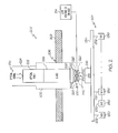
- FIG 2 is a detailed block diagram of an example of an EMI-resistant control device 200 for providing a control signal in accordance with an embodiment of the present disclosure.
- the EMI-resistant control device 200 may include an optical glass fiber connector housing 202.
- the optical glass fiber connector housing 202 may be adapted to be connectable to an apparatus 204 for providing the control signal to the apparatus 204 for controlling operation thereof.
- the EMI-resistant control device 200 may be inserted into an opening 206 formed in a casing 208, housing or packaging of the apparatus 204.
- the apparatus 204 may be an electrical power switching apparatus, such as electrical power switching apparatus 104 of Figure 1 or electrical power switching apparatus 300 of Figure 3 .
- the EMI-resistant control device 200 may also include a carbon nanotube optical switch 210 mounted in the optical glass fiber connector housing 202.
- the carbon nanotube optical switch 210 may include a plurality of light sensitive carbon nanotubes 212. Similar to that previously described, the light sensitive carbon nanotubes 212 are adapted to connect a voltage source 214 to an output 216 of the EMI-resistant control device 200 in response to an optical signal 218 being received by the optical glass fiber connector housing 202.
- the optical glass fiber connector housing 202 includes a structure to direct the optical signal 218 onto the plurality of light sensitive carbon nanotubes 212. The light sensitive carbon nanotubes 212 then become conductive to connect the voltage source 214 to the apparatus 204 to provide the control signal for operation of the apparatus 204.
- the apparatus 204 may be an electrical power switching apparatus to conduct electrical power.
- the carbon nanotube optical switch 210 may include a supporting matrix 218 for retaining the light sensitive carbon nanotubes 212 for substantially each of the carbon nanotubes 212 to receive a predetermined level of photon energy in the optical signal 218 to cause the light sensitive carbon nanotubes 212 to conduct electrical energy or power.
- the light sensitive carbon nanotubes 212 are adapted to be insensitive to electromagnetic radiation of frequencies lower than a frequency of light energy for triggering the light sensitive carbon nanotubes 212 to conduct electric current.
- Each of the plurality of light sensitive carbon nanotubes 212 may include a coating 220 of molecules of a selected material that changes its electronic configuration in response to light to conduct electrical current but is not affected by radio frequency signals or energy.
- An example of a light sensitive carbon nanotube similar to that described herein that may be used for the light sensitive carbon nanotubes 212 are those available from Pettit Applied Technologies, Inc. of Gaithersburg, Maryland.
- EMI-resistant control device 200 may also include an optical glass fiber 222 mounted in the optical glass fiber connector housing 202 to receive the optical signal 218 8 and to transfer the optical signal 218 to the carbon nanotube optical switch 210.
- the optical glass fiber 222 may extend out of the glass fiber connector housing 222 to receive or interface to an optical waveguide 224 that is releasably attachable to the optical glass fiber connector housing 202 for delivering the optical signal 218 to the optical glass fiber 222.
- the optical waveguide 222 may be adapted to have a cutoff frequency of, for example, about 100 GHz (gigahertz) so as to block all signals below that frequency.
- the EMI-resistant control device 200 may also include an optical transmission medium 226, such as a glass section or tube, or other optical transmission medium, mounted in the optical glass fiber connector housing 202 between the optical glass fiber 222 and the carbon nanotube switch 210.
- the optical transmission medium 226 may be adapted to transfer the optical signal 21$ from the optical glass fiber 222 to the carbon nanotube optical switch 210.
- An interface 228 may join or bond the optical transmission medium 226 or glass tube to the carbon nanotube optical switch 210 for efficient transmission of the optical signal 218 photon energy to the carbon nanotube optical switch 210 with low loss and reflection of the signal.
- the apparatus 204 may be an electrical power switching apparatus.
- the apparatus 204 may include a multiplicity of electronic switching units 230. Similar to that previously described, each of the electronic switching units 230 may be an IGBT, FET or similar electronic switching device.
- a gate or gate terminal 232 may be connected to a metal trace 234 or bus which is connected to the output 216 of the carbon nanotube optical switch 210.
- the source (S) and drain (D) of each adjacent IGBT or FET in a chain or row, such as row or chain 134 in Figure 1 may be connected in series similar to that previously described.
- the carbon nanotube switch 210 closes or conducts to connect the voltage source 214 to the line trace 234.
- each switching unit 230 The voltage is then applied to the gate 232 of each switching unit 230, IGBT or FET to activate or close each switching unit 230 to connect an electrical power source or voltage source, such as source 106, to an electrically operated device, such as device 10$ in Figure 1 .
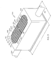
- FIG 3 is an illustration of an example of an electrical power switching apparatus 300 controllable by an EMI-resistant control device in accordance with an embodiment of the present disclosure.
- the electrical power switching apparatus 300 may be used for the electrical power switching apparatus 104 in Figure 1 or the apparatus 204 in Figure 2 .
- the electrical power switching apparatus 300 may include a case 302 or housing.
- the case 302 may be formed from a metallic or dielectric material.
- the case 302 may be made from or may include an EMI shielding material to provide EMI resistance or reduce EMI affects.
- the case 302 may be substantially rectangular in shape and may have a predetermined length (L) and width (W).
- the case 302 may have a length L of about 2 inches and width W of about 1 inch to minimize the volume and weight of the electrical switching apparatus 300.
- the case 302 is shown in Figure 3 with an portion of a top side 304 of the case 302 removed to reveal a multiplicity of miniature electronic switching units 306 enclosed with the case 302.
- the multiplicity of miniature electronic switching units 306 are substantially completely enclosed within the case 302 when installed in a vehicle, such as the vehicle 102 in Figure 1 .
- the electrical power switching apparatus 300 may include an input 308, such as a high voltage or a high power input that may be coupled to an electrical power source or voltage source, such as electrical power or voltage source 106 in Figure 1 .
- the electrical power switching apparatus 300 may also include an output 310, such as a high voltage or high power output that may be coupled to an electrical device, such as electrical device 108 in Figure 1 .
- the electrical power switching apparatus 300 may include a multiplicity of electronic switching units 306.
- the electronic switching units 306 may be electrically connected together in a predetermined circuit configuration 308 for conducting an electric current through the electrical power switching apparatus 300 having a substantially higher amplitude than each individual electronic switching unit 306 is capable of conducting.
- the predetermined circuit configuration may also permit the electrical power switching apparatus 300 to connect a voltage having an amplitude substantially higher than each individual electronic switching unit 230 is capable of connecting to an electrical device for powering the device.
- Each electronic switching units 306 may be an IGBT, FET, or other electronic switching device.
- the predetermined circuit configuration 308 may include a plurality of chains 310 or rows of electronic switching units 306.
- the electronic switching units 306 in each chain 310 are connected in series to provide a voltage standoff capacity of a predetermined voltage amplitude.
- the plurality of chains 310 of the series connected electronic switching units 306 are connected in parallel for the electrical power switching apparatus 300 to provide a current carrying capacity of a predetermined current amplitude.
- the plurality of chains 310 may be connected in parallel by an electrical connection or bus, similar to connections or buses 132 and 136 in Figure 1 at opposite ends of each chain 310.
- An optical trigger 312 may be positioned proximate to a central location of the predetermined electrical configuration 308 of the multiplicity of electronic switching units 306.
- the optical trigger 312 may be an EMI-resistant control device similar to the EMI-resistant control device 200 described with reference to Figure 2 .
- the electrical power switching apparatus 300 may also include an array of metal traces 314 coupled to the optical trigger 312 to provide a control contact to a gate of each electronic switching unit 306 similar to that described with respect to the electronic switching units 122 and 230 in Figures 1 and 2 respectively.
- the metal traces 314 may include a pair primary metal traces 316 and 318 extending laterally from the optical trigger 312 across the casing 302 to each outermost chain 310 of electronic switching units 306.
- a plurality of secondary metal traces 320 may extend from the primary metal traces 316 and 318.
- the secondary metal traces 320 may extend along each chain 310 of series connected electronic switching units 306 to provide the control contact to the gate of each electronic switching unit 306.
- an electrical power switching system such as system 100 in Figure 1 including an EMI-resistant control device, such as device 200 in Figure 2 may substantially replace conventional electrical or copper signal and control wiring used in many current subsystems in aircraft or any type vehicles.
- the power switching system 100 and control device 200 would reduce weight and volumes, while providing intrinsic EME resistance compared to current wired subsystems.
- the EME resistance would be maintained throughout the life of the aircraft or vehicle, because the optic-to-electric signal conversion equipment will be inherently resistant to electromagnetic effects, rather than relying on a shielded enclosure for protection.
- the inherent resistance comes from the fact that certain carbon nanotube-based systems can be made sensitive to light while maintaining the inherent insensitivity of carbon nanotubes to electromagnetic radiation of frequencies lower than the light which is intended to trigger the system 100.
- the EMI-resistant control device as described herein also directly couples the photonic switch, which converts the optical signal into an electrical current flow, into the base of a solid state electric switch, such as electrical switching apparatus 300 of Figure 3 so that this connection can be made with familiar "bonding" processes, used by semiconductor device manufacturers of FETs and IGBTs.
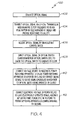
- Figure 4 is a flow chart of an example of a method 400 for providing a control signal in accordance with an embodiment of the present disclosure.
- the control signal is resistant to EMI or EME.
- the method 400 may be embodied in or performed by the system 100 of Figure 1 .
- an optical signal may be generated.
- the optical signal may be transmitted via an optical transmission medium having a cutoff frequency to block penetration of electromagnetic energy and provide resistance to electromagnetic interference.
- the optical signal may be received by an EMI-resistant control device.
- the EMI-resistant control device may be similar to that described in Figure 2 .
- the optical signal may be directed onto an optical switch to cause the optical switch to operate or close.
- the optical switch may be a carbon nanotube optical switch housed within the EMI-resistant control device.
- a voltage source may be connected to an electrical power switching apparatus to cause the electrical power switching apparatus to operate or close in response to the optical switch being operated or closed.
- a signal source may be connected to a device or apparatus being controlled in response to the optical switch being operated or closed.
- an electrical voltage or power source may be connected to a load in response to the electrical power switching apparatus in block 410 becoming operable or closing.
- the load may be an electrically operated device, and aircraft actuator, pump, motor, or other electrically operated device.
Landscapes
- Engineering & Computer Science (AREA)
- Chemical & Material Sciences (AREA)
- Nanotechnology (AREA)
- Physics & Mathematics (AREA)
- Crystallography & Structural Chemistry (AREA)
- General Physics & Mathematics (AREA)
- Composite Materials (AREA)
- Condensed Matter Physics & Semiconductors (AREA)
- Materials Engineering (AREA)
- Mathematical Physics (AREA)
- Theoretical Computer Science (AREA)
- Optics & Photonics (AREA)
- Shielding Devices Or Components To Electric Or Magnetic Fields (AREA)
- Electronic Switches (AREA)
- Optical Couplings Of Light Guides (AREA)
- Endoscopes (AREA)
Applications Claiming Priority (1)
| Application Number | Priority Date | Filing Date | Title |
|---|---|---|---|
| US12/689,490 US8217331B2 (en) | 2010-01-19 | 2010-01-19 | Electromagnetic interference-resistant control device |
Publications (3)
| Publication Number | Publication Date |
|---|---|
| EP2348635A2 true EP2348635A2 (de) | 2011-07-27 |
| EP2348635A3 EP2348635A3 (de) | 2015-06-10 |
| EP2348635B1 EP2348635B1 (de) | 2022-09-21 |
Family
ID=43858248
Family Applications (1)
| Application Number | Title | Priority Date | Filing Date |
|---|---|---|---|
| EP11151214.1A Active EP2348635B1 (de) | 2010-01-19 | 2011-01-18 | Elektromagnetische störungssichere Steuerungsvorrichtung und Verfahren |
Country Status (2)
| Country | Link |
|---|---|
| US (1) | US8217331B2 (de) |
| EP (1) | EP2348635B1 (de) |
Cited By (1)
| Publication number | Priority date | Publication date | Assignee | Title |
|---|---|---|---|---|
| CN112060798A (zh) * | 2020-08-17 | 2020-12-11 | 黄大辉 | 一种智能订书机用订钉帮扶机构 |
Families Citing this family (5)
| Publication number | Priority date | Publication date | Assignee | Title |
|---|---|---|---|---|
| CN101466252B (zh) * | 2007-12-21 | 2011-11-30 | 清华大学 | 电磁屏蔽层及其制备方法 |
| KR101247268B1 (ko) * | 2011-08-01 | 2013-03-25 | 에스케이하이닉스 주식회사 | 반도체 장치 |
| US10108069B2 (en) | 2017-01-24 | 2018-10-23 | The Boeing Company | Electromagnetic effect resistant spatial light modulator |
| US11804839B1 (en) * | 2020-01-28 | 2023-10-31 | Government Of The United States As Represented By The Secretary Of The Air Force | Integrated trigger photoconductive semiconductor switch |
| US12415601B2 (en) * | 2022-11-29 | 2025-09-16 | Textron Innovations Inc. | Electrically isolated auxiliary flight controllers for rotorcraft |
Family Cites Families (9)
| Publication number | Priority date | Publication date | Assignee | Title |
|---|---|---|---|---|
| ITTO20030425A1 (it) * | 2003-06-06 | 2004-12-07 | St Microelectronics Srl | Dispositivo interruttore elettrico a comando ottico basato su nanotubi di carbonio e sistema interruttore elettrico utilizzante tale dispositivo interruttore. |
| JP4296252B2 (ja) * | 2003-07-18 | 2009-07-15 | 独立行政法人科学技術振興機構 | 光検出素子 |
| JP4154671B2 (ja) * | 2003-09-17 | 2008-09-24 | 富士電機ホールディングス株式会社 | 電力用半導体モジュール |
| US8013359B2 (en) * | 2003-12-31 | 2011-09-06 | John W. Pettit | Optically controlled electrical switching device based on wide bandgap semiconductors |
| US20050218398A1 (en) * | 2004-04-06 | 2005-10-06 | Availableip.Com | NANO-electronics |
| WO2007002603A2 (en) * | 2005-06-24 | 2007-01-04 | The Board Of Trustees Of The University Of Illinois | Optically-triggered power system and devices |
| US7649665B2 (en) * | 2005-08-24 | 2010-01-19 | The Trustees Of Boston College | Apparatus and methods for optical switching using nanoscale optics |
| US8570636B2 (en) * | 2008-04-18 | 2013-10-29 | Zikon Inc. | Systems, methods and compositions relating to display elements |
| US8946848B2 (en) * | 2008-06-05 | 2015-02-03 | Omnivision Technologies, Inc. | Apparatus and method for image sensor with carbon nanotube based transparent conductive coating |
-
2010
- 2010-01-19 US US12/689,490 patent/US8217331B2/en active Active
-
2011
- 2011-01-18 EP EP11151214.1A patent/EP2348635B1/de active Active
Non-Patent Citations (1)
| Title |
|---|
| None |
Cited By (1)
| Publication number | Priority date | Publication date | Assignee | Title |
|---|---|---|---|---|
| CN112060798A (zh) * | 2020-08-17 | 2020-12-11 | 黄大辉 | 一种智能订书机用订钉帮扶机构 |
Also Published As
| Publication number | Publication date |
|---|---|
| US8217331B2 (en) | 2012-07-10 |
| US20110174960A1 (en) | 2011-07-21 |
| EP2348635B1 (de) | 2022-09-21 |
| EP2348635A3 (de) | 2015-06-10 |
Similar Documents
| Publication | Publication Date | Title |
|---|---|---|
| EP2348635B1 (de) | Elektromagnetische störungssichere Steuerungsvorrichtung und Verfahren | |
| US7400791B2 (en) | Semiconductor element mounting board and optical transmission module | |
| US6758607B2 (en) | Optical communication module and optical communication module product | |
| US9755379B1 (en) | Capacitively coupled connector junctions having parallel signal paths and related connectors and methods | |
| KR20210002770U (ko) | 광 모듈 및 차량 헤드램프 | |
| US20200014087A1 (en) | Plug connector for connecting a waveguide to at least one electric conductor | |
| JPS643397B2 (de) | ||
| CN108631042B (zh) | 天线组件及电子装置 | |
| EP0108391B1 (de) | Optische Steuereinrichtung | |
| EP2744054B1 (de) | Verbindungsstruktur zur Kopplung einer elektronischen Einheit und einer optischen Einheit sowie optoelektronisches Modul | |
| CN113671636B (zh) | 光模块 | |
| CN109076697A (zh) | 印刷电路板及包括该印刷电路板的电子元件封装 | |
| US7026545B2 (en) | Flex cable having a return-signal path and method for reducing length and impedance of a return-signal path | |
| JP2544227B2 (ja) | 電気光学モジュ―ルの過渡電圧放電機構 | |
| US6366380B1 (en) | Optical transceiver EMI detuning device | |
| US6417719B1 (en) | Apparatus and method for isolating a trigger circuit of a silicon-controlled rectifier | |
| US8963366B2 (en) | System for power transmission | |
| US11565593B2 (en) | Holding apparatus for current and signal conductors of a traction battery of a motor vehicle | |
| CN114093953A (zh) | 光模块 | |
| EP0904546A2 (de) | Messsystem mit antenne | |
| KR102629222B1 (ko) | 채널 모듈 간의 간섭을 최소화한 배터리 사이클러 | |
| JP7051409B2 (ja) | 光送信モジュール及び光モジュール | |
| CN1989625A (zh) | 光接收装置 | |
| JP2002154490A (ja) | ヘリコプター搭載配電設備における電力開閉装置(apowerswitchingdevice) | |
| KR20180076013A (ko) | 항공기용 매트릭스 장치 |
Legal Events
| Date | Code | Title | Description |
|---|---|---|---|
| PUAI | Public reference made under article 153(3) epc to a published international application that has entered the european phase |
Free format text: ORIGINAL CODE: 0009012 |
|
| 17P | Request for examination filed |
Effective date: 20110118 |
|
| AK | Designated contracting states |
Kind code of ref document: A2 Designated state(s): AL AT BE BG CH CY CZ DE DK EE ES FI FR GB GR HR HU IE IS IT LI LT LU LV MC MK MT NL NO PL PT RO RS SE SI SK SM TR |
|
| AX | Request for extension of the european patent |
Extension state: BA ME |
|
| PUAL | Search report despatched |
Free format text: ORIGINAL CODE: 0009013 |
|
| AK | Designated contracting states |
Kind code of ref document: A3 Designated state(s): AL AT BE BG CH CY CZ DE DK EE ES FI FR GB GR HR HU IE IS IT LI LT LU LV MC MK MT NL NO PL PT RO RS SE SI SK SM TR |
|
| AX | Request for extension of the european patent |
Extension state: BA ME |
|
| RIC1 | Information provided on ipc code assigned before grant |
Ipc: B82Y 30/00 20110101ALI20150507BHEP Ipc: B82Y 20/00 20110101ALI20150507BHEP Ipc: H03K 3/57 20060101AFI20150507BHEP Ipc: G02B 6/42 20060101ALI20150507BHEP Ipc: G02F 1/1333 20060101ALI20150507BHEP Ipc: B82Y 10/00 20110101ALI20150507BHEP |
|
| STAA | Information on the status of an ep patent application or granted ep patent |
Free format text: STATUS: EXAMINATION IS IN PROGRESS |
|
| 17Q | First examination report despatched |
Effective date: 20181010 |
|
| GRAP | Despatch of communication of intention to grant a patent |
Free format text: ORIGINAL CODE: EPIDOSNIGR1 |
|
| STAA | Information on the status of an ep patent application or granted ep patent |
Free format text: STATUS: GRANT OF PATENT IS INTENDED |
|
| INTG | Intention to grant announced |
Effective date: 20220519 |
|
| GRAS | Grant fee paid |
Free format text: ORIGINAL CODE: EPIDOSNIGR3 |
|
| GRAA | (expected) grant |
Free format text: ORIGINAL CODE: 0009210 |
|
| STAA | Information on the status of an ep patent application or granted ep patent |
Free format text: STATUS: THE PATENT HAS BEEN GRANTED |
|
| AK | Designated contracting states |
Kind code of ref document: B1 Designated state(s): AL AT BE BG CH CY CZ DE DK EE ES FI FR GB GR HR HU IE IS IT LI LT LU LV MC MK MT NL NO PL PT RO RS SE SI SK SM TR |
|
| REG | Reference to a national code |
Ref country code: GB Ref legal event code: FG4D |
|
| REG | Reference to a national code |
Ref country code: CH Ref legal event code: EP |
|
| REG | Reference to a national code |
Ref country code: IE Ref legal event code: FG4D |
|
| REG | Reference to a national code |
Ref country code: DE Ref legal event code: R096 Ref document number: 602011073298 Country of ref document: DE |
|
| REG | Reference to a national code |
Ref country code: AT Ref legal event code: REF Ref document number: 1520473 Country of ref document: AT Kind code of ref document: T Effective date: 20221015 |
|
| REG | Reference to a national code |
Ref country code: LT Ref legal event code: MG9D |
|
| REG | Reference to a national code |
Ref country code: NL Ref legal event code: MP Effective date: 20220921 |
|
| PG25 | Lapsed in a contracting state [announced via postgrant information from national office to epo] |
Ref country code: SE Free format text: LAPSE BECAUSE OF FAILURE TO SUBMIT A TRANSLATION OF THE DESCRIPTION OR TO PAY THE FEE WITHIN THE PRESCRIBED TIME-LIMIT Effective date: 20220921 Ref country code: RS Free format text: LAPSE BECAUSE OF FAILURE TO SUBMIT A TRANSLATION OF THE DESCRIPTION OR TO PAY THE FEE WITHIN THE PRESCRIBED TIME-LIMIT Effective date: 20220921 Ref country code: NO Free format text: LAPSE BECAUSE OF FAILURE TO SUBMIT A TRANSLATION OF THE DESCRIPTION OR TO PAY THE FEE WITHIN THE PRESCRIBED TIME-LIMIT Effective date: 20221221 Ref country code: LV Free format text: LAPSE BECAUSE OF FAILURE TO SUBMIT A TRANSLATION OF THE DESCRIPTION OR TO PAY THE FEE WITHIN THE PRESCRIBED TIME-LIMIT Effective date: 20220921 Ref country code: LT Free format text: LAPSE BECAUSE OF FAILURE TO SUBMIT A TRANSLATION OF THE DESCRIPTION OR TO PAY THE FEE WITHIN THE PRESCRIBED TIME-LIMIT Effective date: 20220921 Ref country code: FI Free format text: LAPSE BECAUSE OF FAILURE TO SUBMIT A TRANSLATION OF THE DESCRIPTION OR TO PAY THE FEE WITHIN THE PRESCRIBED TIME-LIMIT Effective date: 20220921 |
|
| REG | Reference to a national code |
Ref country code: AT Ref legal event code: MK05 Ref document number: 1520473 Country of ref document: AT Kind code of ref document: T Effective date: 20220921 |
|
| PG25 | Lapsed in a contracting state [announced via postgrant information from national office to epo] |
Ref country code: HR Free format text: LAPSE BECAUSE OF FAILURE TO SUBMIT A TRANSLATION OF THE DESCRIPTION OR TO PAY THE FEE WITHIN THE PRESCRIBED TIME-LIMIT Effective date: 20220921 Ref country code: GR Free format text: LAPSE BECAUSE OF FAILURE TO SUBMIT A TRANSLATION OF THE DESCRIPTION OR TO PAY THE FEE WITHIN THE PRESCRIBED TIME-LIMIT Effective date: 20221222 |
|
| RAP4 | Party data changed (patent owner data changed or rights of a patent transferred) |
Owner name: THE BOEING COMPANY |
|
| PG25 | Lapsed in a contracting state [announced via postgrant information from national office to epo] |
Ref country code: SM Free format text: LAPSE BECAUSE OF FAILURE TO SUBMIT A TRANSLATION OF THE DESCRIPTION OR TO PAY THE FEE WITHIN THE PRESCRIBED TIME-LIMIT Effective date: 20220921 Ref country code: RO Free format text: LAPSE BECAUSE OF FAILURE TO SUBMIT A TRANSLATION OF THE DESCRIPTION OR TO PAY THE FEE WITHIN THE PRESCRIBED TIME-LIMIT Effective date: 20220921 Ref country code: PT Free format text: LAPSE BECAUSE OF FAILURE TO SUBMIT A TRANSLATION OF THE DESCRIPTION OR TO PAY THE FEE WITHIN THE PRESCRIBED TIME-LIMIT Effective date: 20230123 Ref country code: ES Free format text: LAPSE BECAUSE OF FAILURE TO SUBMIT A TRANSLATION OF THE DESCRIPTION OR TO PAY THE FEE WITHIN THE PRESCRIBED TIME-LIMIT Effective date: 20220921 Ref country code: CZ Free format text: LAPSE BECAUSE OF FAILURE TO SUBMIT A TRANSLATION OF THE DESCRIPTION OR TO PAY THE FEE WITHIN THE PRESCRIBED TIME-LIMIT Effective date: 20220921 Ref country code: AT Free format text: LAPSE BECAUSE OF FAILURE TO SUBMIT A TRANSLATION OF THE DESCRIPTION OR TO PAY THE FEE WITHIN THE PRESCRIBED TIME-LIMIT Effective date: 20220921 |
|
| PG25 | Lapsed in a contracting state [announced via postgrant information from national office to epo] |
Ref country code: SK Free format text: LAPSE BECAUSE OF FAILURE TO SUBMIT A TRANSLATION OF THE DESCRIPTION OR TO PAY THE FEE WITHIN THE PRESCRIBED TIME-LIMIT Effective date: 20220921 Ref country code: PL Free format text: LAPSE BECAUSE OF FAILURE TO SUBMIT A TRANSLATION OF THE DESCRIPTION OR TO PAY THE FEE WITHIN THE PRESCRIBED TIME-LIMIT Effective date: 20220921 Ref country code: IS Free format text: LAPSE BECAUSE OF FAILURE TO SUBMIT A TRANSLATION OF THE DESCRIPTION OR TO PAY THE FEE WITHIN THE PRESCRIBED TIME-LIMIT Effective date: 20230121 Ref country code: EE Free format text: LAPSE BECAUSE OF FAILURE TO SUBMIT A TRANSLATION OF THE DESCRIPTION OR TO PAY THE FEE WITHIN THE PRESCRIBED TIME-LIMIT Effective date: 20220921 |
|
| P01 | Opt-out of the competence of the unified patent court (upc) registered |
Effective date: 20230516 |
|
| REG | Reference to a national code |
Ref country code: DE Ref legal event code: R097 Ref document number: 602011073298 Country of ref document: DE |
|
| PG25 | Lapsed in a contracting state [announced via postgrant information from national office to epo] |
Ref country code: NL Free format text: LAPSE BECAUSE OF FAILURE TO SUBMIT A TRANSLATION OF THE DESCRIPTION OR TO PAY THE FEE WITHIN THE PRESCRIBED TIME-LIMIT Effective date: 20220921 Ref country code: AL Free format text: LAPSE BECAUSE OF FAILURE TO SUBMIT A TRANSLATION OF THE DESCRIPTION OR TO PAY THE FEE WITHIN THE PRESCRIBED TIME-LIMIT Effective date: 20220921 |
|
| PLBE | No opposition filed within time limit |
Free format text: ORIGINAL CODE: 0009261 |
|
| STAA | Information on the status of an ep patent application or granted ep patent |
Free format text: STATUS: NO OPPOSITION FILED WITHIN TIME LIMIT |
|
| PG25 | Lapsed in a contracting state [announced via postgrant information from national office to epo] |
Ref country code: DK Free format text: LAPSE BECAUSE OF FAILURE TO SUBMIT A TRANSLATION OF THE DESCRIPTION OR TO PAY THE FEE WITHIN THE PRESCRIBED TIME-LIMIT Effective date: 20220921 |
|
| 26N | No opposition filed |
Effective date: 20230622 |
|
| PG25 | Lapsed in a contracting state [announced via postgrant information from national office to epo] |
Ref country code: SI Free format text: LAPSE BECAUSE OF FAILURE TO SUBMIT A TRANSLATION OF THE DESCRIPTION OR TO PAY THE FEE WITHIN THE PRESCRIBED TIME-LIMIT Effective date: 20220921 |
|
| REG | Reference to a national code |
Ref country code: CH Ref legal event code: PL |
|
| PG25 | Lapsed in a contracting state [announced via postgrant information from national office to epo] |
Ref country code: LU Free format text: LAPSE BECAUSE OF NON-PAYMENT OF DUE FEES Effective date: 20230118 |
|
| REG | Reference to a national code |
Ref country code: BE Ref legal event code: MM Effective date: 20230131 |
|
| PG25 | Lapsed in a contracting state [announced via postgrant information from national office to epo] |
Ref country code: LI Free format text: LAPSE BECAUSE OF NON-PAYMENT OF DUE FEES Effective date: 20230131 Ref country code: CH Free format text: LAPSE BECAUSE OF NON-PAYMENT OF DUE FEES Effective date: 20230131 |
|
| PG25 | Lapsed in a contracting state [announced via postgrant information from national office to epo] |
Ref country code: BE Free format text: LAPSE BECAUSE OF NON-PAYMENT OF DUE FEES Effective date: 20230131 |
|
| PG25 | Lapsed in a contracting state [announced via postgrant information from national office to epo] |
Ref country code: IE Free format text: LAPSE BECAUSE OF NON-PAYMENT OF DUE FEES Effective date: 20230118 |
|
| PG25 | Lapsed in a contracting state [announced via postgrant information from national office to epo] |
Ref country code: IT Free format text: LAPSE BECAUSE OF FAILURE TO SUBMIT A TRANSLATION OF THE DESCRIPTION OR TO PAY THE FEE WITHIN THE PRESCRIBED TIME-LIMIT Effective date: 20220921 |
|
| PG25 | Lapsed in a contracting state [announced via postgrant information from national office to epo] |
Ref country code: MC Free format text: LAPSE BECAUSE OF FAILURE TO SUBMIT A TRANSLATION OF THE DESCRIPTION OR TO PAY THE FEE WITHIN THE PRESCRIBED TIME-LIMIT Effective date: 20220921 |
|
| PG25 | Lapsed in a contracting state [announced via postgrant information from national office to epo] |
Ref country code: MC Free format text: LAPSE BECAUSE OF FAILURE TO SUBMIT A TRANSLATION OF THE DESCRIPTION OR TO PAY THE FEE WITHIN THE PRESCRIBED TIME-LIMIT Effective date: 20220921 |
|
| PG25 | Lapsed in a contracting state [announced via postgrant information from national office to epo] |
Ref country code: BG Free format text: LAPSE BECAUSE OF FAILURE TO SUBMIT A TRANSLATION OF THE DESCRIPTION OR TO PAY THE FEE WITHIN THE PRESCRIBED TIME-LIMIT Effective date: 20220921 |
|
| PG25 | Lapsed in a contracting state [announced via postgrant information from national office to epo] |
Ref country code: BG Free format text: LAPSE BECAUSE OF FAILURE TO SUBMIT A TRANSLATION OF THE DESCRIPTION OR TO PAY THE FEE WITHIN THE PRESCRIBED TIME-LIMIT Effective date: 20220921 |
|
| PGFP | Annual fee paid to national office [announced via postgrant information from national office to epo] |
Ref country code: DE Payment date: 20250129 Year of fee payment: 15 |
|
| PGFP | Annual fee paid to national office [announced via postgrant information from national office to epo] |
Ref country code: FR Payment date: 20250127 Year of fee payment: 15 |
|
| PGFP | Annual fee paid to national office [announced via postgrant information from national office to epo] |
Ref country code: GB Payment date: 20250127 Year of fee payment: 15 |
|
| PG25 | Lapsed in a contracting state [announced via postgrant information from national office to epo] |
Ref country code: CY Free format text: LAPSE BECAUSE OF FAILURE TO SUBMIT A TRANSLATION OF THE DESCRIPTION OR TO PAY THE FEE WITHIN THE PRESCRIBED TIME-LIMIT; INVALID AB INITIO Effective date: 20110118 |
|
| PG25 | Lapsed in a contracting state [announced via postgrant information from national office to epo] |
Ref country code: HU Free format text: LAPSE BECAUSE OF FAILURE TO SUBMIT A TRANSLATION OF THE DESCRIPTION OR TO PAY THE FEE WITHIN THE PRESCRIBED TIME-LIMIT; INVALID AB INITIO Effective date: 20110118 |
|
| PG25 | Lapsed in a contracting state [announced via postgrant information from national office to epo] |
Ref country code: TR Free format text: LAPSE BECAUSE OF FAILURE TO SUBMIT A TRANSLATION OF THE DESCRIPTION OR TO PAY THE FEE WITHIN THE PRESCRIBED TIME-LIMIT Effective date: 20220921 |