EP2348622A1 - Dc-dc converter - Google Patents
Dc-dc converter Download PDFInfo
- Publication number
- EP2348622A1 EP2348622A1 EP08811042A EP08811042A EP2348622A1 EP 2348622 A1 EP2348622 A1 EP 2348622A1 EP 08811042 A EP08811042 A EP 08811042A EP 08811042 A EP08811042 A EP 08811042A EP 2348622 A1 EP2348622 A1 EP 2348622A1
- Authority
- EP
- European Patent Office
- Prior art keywords
- voltage
- dcdc converter
- capacitor
- control unit
- smoothing
- Prior art date
- Legal status (The legal status is an assumption and is not a legal conclusion. Google has not performed a legal analysis and makes no representation as to the accuracy of the status listed.)
- Granted
Links
- 239000003990 capacitor Substances 0.000 claims abstract description 101
- 238000009499 grossing Methods 0.000 claims abstract description 90
- 238000013016 damping Methods 0.000 claims abstract description 73
- HEZMWWAKWCSUCB-PHDIDXHHSA-N (3R,4R)-3,4-dihydroxycyclohexa-1,5-diene-1-carboxylic acid Chemical compound O[C@@H]1C=CC(C(O)=O)=C[C@H]1O HEZMWWAKWCSUCB-PHDIDXHHSA-N 0.000 claims abstract description 63
- 230000010355 oscillation Effects 0.000 description 33
- 238000010586 diagram Methods 0.000 description 20
- 230000014509 gene expression Effects 0.000 description 5
- 230000007423 decrease Effects 0.000 description 4
- 230000000694 effects Effects 0.000 description 3
- 238000005516 engineering process Methods 0.000 description 3
- 230000000087 stabilizing effect Effects 0.000 description 3
- 238000000034 method Methods 0.000 description 2
- 230000006641 stabilisation Effects 0.000 description 2
- 238000011105 stabilization Methods 0.000 description 2
- 230000001629 suppression Effects 0.000 description 2
- 230000001052 transient effect Effects 0.000 description 2
- NAWXUBYGYWOOIX-SFHVURJKSA-N (2s)-2-[[4-[2-(2,4-diaminoquinazolin-6-yl)ethyl]benzoyl]amino]-4-methylidenepentanedioic acid Chemical compound C1=CC2=NC(N)=NC(N)=C2C=C1CCC1=CC=C(C(=O)N[C@@H](CC(=C)C(O)=O)C(O)=O)C=C1 NAWXUBYGYWOOIX-SFHVURJKSA-N 0.000 description 1
- HBBGRARXTFLTSG-UHFFFAOYSA-N Lithium ion Chemical compound [Li+] HBBGRARXTFLTSG-UHFFFAOYSA-N 0.000 description 1
- 238000001914 filtration Methods 0.000 description 1
- 229910052739 hydrogen Inorganic materials 0.000 description 1
- 239000001257 hydrogen Substances 0.000 description 1
- 229910001416 lithium ion Inorganic materials 0.000 description 1
- 229910052759 nickel Inorganic materials 0.000 description 1
- PXHVJJICTQNCMI-UHFFFAOYSA-N nickel Substances [Ni] PXHVJJICTQNCMI-UHFFFAOYSA-N 0.000 description 1
- -1 nickel hydrogen Chemical class 0.000 description 1
Images


Classifications
-
- H—ELECTRICITY
- H02—GENERATION; CONVERSION OR DISTRIBUTION OF ELECTRIC POWER
- H02M—APPARATUS FOR CONVERSION BETWEEN AC AND AC, BETWEEN AC AND DC, OR BETWEEN DC AND DC, AND FOR USE WITH MAINS OR SIMILAR POWER SUPPLY SYSTEMS; CONVERSION OF DC OR AC INPUT POWER INTO SURGE OUTPUT POWER; CONTROL OR REGULATION THEREOF
- H02M3/00—Conversion of dc power input into dc power output
- H02M3/02—Conversion of dc power input into dc power output without intermediate conversion into ac
- H02M3/04—Conversion of dc power input into dc power output without intermediate conversion into ac by static converters
- H02M3/10—Conversion of dc power input into dc power output without intermediate conversion into ac by static converters using discharge tubes with control electrode or semiconductor devices with control electrode
- H02M3/145—Conversion of dc power input into dc power output without intermediate conversion into ac by static converters using discharge tubes with control electrode or semiconductor devices with control electrode using devices of a triode or transistor type requiring continuous application of a control signal
- H02M3/155—Conversion of dc power input into dc power output without intermediate conversion into ac by static converters using discharge tubes with control electrode or semiconductor devices with control electrode using devices of a triode or transistor type requiring continuous application of a control signal using semiconductor devices only
- H02M3/156—Conversion of dc power input into dc power output without intermediate conversion into ac by static converters using discharge tubes with control electrode or semiconductor devices with control electrode using devices of a triode or transistor type requiring continuous application of a control signal using semiconductor devices only with automatic control of output voltage or current, e.g. switching regulators
-
- B—PERFORMING OPERATIONS; TRANSPORTING
- B60—VEHICLES IN GENERAL
- B60L—PROPULSION OF ELECTRICALLY-PROPELLED VEHICLES; SUPPLYING ELECTRIC POWER FOR AUXILIARY EQUIPMENT OF ELECTRICALLY-PROPELLED VEHICLES; ELECTRODYNAMIC BRAKE SYSTEMS FOR VEHICLES IN GENERAL; MAGNETIC SUSPENSION OR LEVITATION FOR VEHICLES; MONITORING OPERATING VARIABLES OF ELECTRICALLY-PROPELLED VEHICLES; ELECTRIC SAFETY DEVICES FOR ELECTRICALLY-PROPELLED VEHICLES
- B60L9/00—Electric propulsion with power supply external to the vehicle
- B60L9/16—Electric propulsion with power supply external to the vehicle using ac induction motors
- B60L9/18—Electric propulsion with power supply external to the vehicle using ac induction motors fed from dc supply lines
-
- H—ELECTRICITY
- H02—GENERATION; CONVERSION OR DISTRIBUTION OF ELECTRIC POWER
- H02M—APPARATUS FOR CONVERSION BETWEEN AC AND AC, BETWEEN AC AND DC, OR BETWEEN DC AND DC, AND FOR USE WITH MAINS OR SIMILAR POWER SUPPLY SYSTEMS; CONVERSION OF DC OR AC INPUT POWER INTO SURGE OUTPUT POWER; CONTROL OR REGULATION THEREOF
- H02M1/00—Details of apparatus for conversion
- H02M1/14—Arrangements for reducing ripples from dc input or output
-
- H—ELECTRICITY
- H02—GENERATION; CONVERSION OR DISTRIBUTION OF ELECTRIC POWER
- H02M—APPARATUS FOR CONVERSION BETWEEN AC AND AC, BETWEEN AC AND DC, OR BETWEEN DC AND DC, AND FOR USE WITH MAINS OR SIMILAR POWER SUPPLY SYSTEMS; CONVERSION OF DC OR AC INPUT POWER INTO SURGE OUTPUT POWER; CONTROL OR REGULATION THEREOF
- H02M1/00—Details of apparatus for conversion
- H02M1/44—Circuits or arrangements for compensating for electromagnetic interference in converters or inverters
-
- H—ELECTRICITY
- H02—GENERATION; CONVERSION OR DISTRIBUTION OF ELECTRIC POWER
- H02M—APPARATUS FOR CONVERSION BETWEEN AC AND AC, BETWEEN AC AND DC, OR BETWEEN DC AND DC, AND FOR USE WITH MAINS OR SIMILAR POWER SUPPLY SYSTEMS; CONVERSION OF DC OR AC INPUT POWER INTO SURGE OUTPUT POWER; CONTROL OR REGULATION THEREOF
- H02M1/00—Details of apparatus for conversion
- H02M1/0003—Details of control, feedback or regulation circuits
- H02M1/0016—Control circuits providing compensation of output voltage deviations using feedforward of disturbance parameters
- H02M1/0022—Control circuits providing compensation of output voltage deviations using feedforward of disturbance parameters the disturbance parameters being input voltage fluctuations
Definitions
- the present invention relates to a DCDC converter suitable for application to, for example, an electric motor car.
- a reactor is provided between the DCDC converter and the overhead wire and attenuation of a harmonic current output from the DCDC converter to the overhead wire side is performed by an LC filter circuit including this reactor and an input capacitor.
- Patent Document Japanese Patent Application Laid-open No. 2007-274756
- the inventor found that, when the DCDC converter is actuated, because, for example, electric oscillation occurs in the LC filter circuit and the input capacitor is subjected to overvoltage, in some case, normal operation of the DCDC converter cannot be performed.
- the present invention has been devised in view of the knowledge of the inventor and it is an object of the present invention to provide a DCDC converter that suppresses electric oscillation occurring in an LC filer circuit and enables stable operation.
- a DCDC converter is constructed in such a manner as to have an input filter circuit including an input reactor connected to a DC power supply and an input capacitor and converts a DC voltage of the input capacitor into an arbitrary DC voltage to output the DC voltage, and further includes: a switching circuit, to an input end of which the input filer circuit is connected, the switching circuit including an upper arm side switching element and a lower arm side switching element; a smoothing filer circuit connected to an output end of the switching circuit; and a control unit that feeds back a state amount of the smoothing filter circuit and controls to turn on and off the switching circuit, wherein the control unit includes a damping control unit that calculates, based on a voltage of the input capacitor, a damping operation amount for adjusting a state amount of the smoothing filter circuit.
- the switching circuit is controlled based on an optimum damping operation amount for controlling electric oscillation occurring in the input filter circuit. Therefore, there is an effect that it is possible to suppress the electric oscillation occurring in the LC input filter circuit and perform stable operation of the DCDC converter.
- FIG. 1 is a diagram of a configuration example of a DCDC converter in a first embodiment of the present invention.
- a DCDC converter 100 is electrically connected to an overhead wire 1, which is connected to a substation (not shown) serving as a DC power supply, via a current collector 2.
- the DCDC converter 100 is also electrically connected to a rail 4, which is connected to the substation, via a wheel 3 serving as a return circuit for a return current.
- the DCDC converter 100 includes a main circuit unit 200 and a control unit 300 that controls a power flow in the main circuit unit 200.
- the main circuit unit 200 includes, as main components, an input filter circuit 8, a voltage detector 7, a switching circuit 10, a smoothing filter circuit 27, a voltage detector 23, a current detector 21, and a power storage element 26.
- the switching circuit 10 includes an upper arm side switching element 11 and a lower arm side switching element 12.
- the input filter circuit 8 includes a reactor 5 as an input reactor and a capacitor 6 as an input capacitor.
- the smoothing filter circuit 27 includes a smoothing reactor 20.
- the switching circuit 10 functions as a power converting circuit in two directions from the overhead wire 1 to the power storage element 26 and from the power storage element 26 to the overhead wire 1.
- the input filter circuit 8 suppresses a harmonic current generated from the switching circuit 10 from flowing out to the substation side via the current collector 2.
- the voltage detector 7 detects a voltage EFC at both ends of the capacitor 6.
- the power storage element 26 accumulates required electric power.
- the voltage detector 23 detects a terminal voltage BFC of the power storage element 26.
- the smoothing filter circuit 27 performs filtering of a current ripple generated from the switching circuit 10.
- the current detector 21 detects an electric current flowing to the smoothing reactor 20 (hereinafter referred to as "smoothing reactor current") ISL.
- An output side of the switching circuit 10 is connected to the power storage element 26 via the smoothing reactor 20 and the current detector 21 with a connection end between the upper arm side switching element 11 and the lower arm side switching element 12 (one end of the upper arm side switching element 11) used as an output end.
- An input side of the switching circuit 10 is connected to the overhead wire 1 via the input filter circuit 8 and the current collector 2 with the other end of the upper arm side switching element 11 used as an input end.
- the power storage element 26 a nickel hydrogen secondary battery, a lithium ion secondary battery, an electric double layer capacitor, or the like is suitable. However, other power storage elements can be used.
- the DC power supply that supplies electric power to the overhead wire 1 the substation is explained as an example. However, the DC power supply can be other DC power supply.
- the control unit 300 includes a control-signal generating unit 50 and a damping control unit 40.
- the control-signal generating unit 50 includes a multiplier 34, a subtracter 35, a current controller 36, a modulation circuit 37, and a damping control unit 40.
- the multiplier 34 performs multiplication of a smoothing reactor current command ISL* input from a host control system (not shown) and a damping operation amount DAMPCN explained later.
- the smoothing reactor current command ISL* is a command value of the smoothing reactor current ISL.
- the subtracter 35 subtracts the smoothing reactor current ISL from an output (ISL**) of the multiplier 34.
- the current controller 36 is input with an output of the subtracter 35 and performs proportional integral control.
- the proportional integral control is suitable.
- the control system can be proportional control.
- the current controller 36 can be configured by a publicly-known technology irrespective of which of the control systems is adopted. Therefore, explanation of the control system is omitted here.
- the modulation circuit 37 outputs, based on an output of the current controller 36, the voltage EFC of the capacitor 6, and the terminal voltage BFC of the power storage element 26, a control signal to the switching circuit 10 (hereinafter referred to as "switching signal") GSG.
- the damping control unit 40 is input with the voltage EFC of the capacitor 6 and outputs the damping operation amount DAMPCN.
- the configuration of the damping control unit 40 is explained later together with the operation thereof.
- the smoothing reactor current command ISL* is the command value of the smoothing reactor current ISL output from the host control system (not shown) as explained above.
- ISL* is set to 0 and the control unit 300 controls the switching circuit 10 of the main circuit unit 200 such that the smoothing reactor current ISL does not flow.
- ISL* is set to a positive value and the control unit 300 controls the switching circuit 10 of the main circuit unit 200 to perform a charge operation such that the smoothing reactor current ISL changes to a power flow from the overhead wire 1 side to the power storage element 26 side.
- ISL* is set to a negative value and the control unit 300 controls the switching circuit 10 of the main circuit unit 200 to perform a discharge operation such that the smoothing reactor current ISL changes to a power flow from the power storage element 26 side to the overhead wire 1 side.
- the DCDC converter 100 functions as a control current source that controls, according to the smoothing reactor current command ISL* output from the host control system, the smoothing reactor current ISL to be a predetermined value and is capable of realizing an arbitrary power flow corresponding to necessity.
- the damping control unit 40 as a main part of this embodiment is explained.
- FIG. 2 is a circuit block diagram in which the main circuit unit 200 shown in FIG. 1 is simplified.
- the overhead wire 1, the current collector 2, the wheel 3, and the rail 4 in FIG. 1 are not shown and the substation is replaced with a DC power supply 70.
- the reactor 5 includes an inductance component L and a resistance component R.
- the capacitance of the capacitor 6 is represented as C.
- the switching circuit 10 is controlled such that the smoothing reactor current ISL is maintained constant even if the voltage EFC of the capacitor 6 fluctuates. In other words, even if the voltage EFC of the capacitor 6 fluctuates, because input power PDC of the switching circuit 10 is controlled not to change, the switching circuit 10 has a constant power characteristic with respect to the fluctuation in the voltage EFC of the capacitor 6. Therefore, blocks including the switching circuit 10, the smoothing reactor 20, and the power storage element 26 are collected as one load viewed from the LC filer side and set as a constant power load 80.
- the constant power load 80 has a negative resistance characteristic that, if the voltage EFC of the capacitor 6 rises, an input current IDC of the switching circuit 10 decreases and, if the voltage EFC of the capacitor 6 falls, the input current IDC of the switching circuit 10 increases.
- a normal resistor (a positive resistor) has a positive resistance characteristic that, if a voltage rises, an electric current increases and, if the voltage falls, the electric current decreases.
- the constant power load 80 has a characteristic opposite to that of the normal resistor in a change of an electric current with respect to a change in a voltage.
- a transfer function of the circuit shown in FIG. 2 is calculated and evaluated and quantitative explanation of the phenomenon qualitatively explained above is made.
- Formula (1) is nonlinear, Formula (1) is linearized.
- EFC0 and IDC0 the following Formula (2) holds near the operating point:
- IDC - PDC ⁇ EFC - EFC ⁇ 0 EFC ⁇ 0 2 + IDC ⁇ 0
- FIG. 3 is a block diagram of a transfer function of the circuit shown in FIG. 2 .
- a closed loop transfer function G(s) from an input voltage ES to the voltage EFC of the capacitor 6 is represented by the following Formula (3):
- G s 1 C ⁇ L s 2 + R L - PDC C ⁇ EFC ⁇ 0 2 ⁇ s - 1 C ⁇ L ⁇ R ⁇ PDC EFC ⁇ 0 2 - 1
- a condition for stabilizing a closed loop system shown in the closed loop transfer function G(s) of Formula (3) is that all poles of G(s) are negative.
- all solutions of a characteristic equation indicated by the following Formula (4), which is the denominator of G(s) need to be negative.
- a conditional expression of the resistance component R of the reactor 5 for stabilizing the closed loop system indicated by the transfer function G(s) of Formula (3) is calculated. Attention is directed to Formula (5) because Formula (6) does not include useful information. When Formula (5) is modified, the following Formula (7) as the conditional expression of the resistance component R of the reactor 5 is obtained.
- R necessary for stabilizing the system can be smaller as L is smaller, C is larger, PDC is smaller, and EFC0 is larger.
- a value of the resistance component R of the reactor 5 that can stabilize the closed loop system indicated by the transfer function G(s) of Formula (3) is R>0.8 ( ⁇ ).
- a resistance component included in a reactor is very small at about several tens (m ⁇ ) and it is impossible to satisfy Formula (7). Therefore, the closed loop system of the circuit shown in FIG. 2 is unstable and electric oscillation occurs at a resonant frequency of the LC filter.
- a resistor that satisfies Formula (7) is added to the circuit shown in FIG. 2 or stabilization of the closed loop system is realized in terms of control, the voltage EFC of the capacitor 6 oscillates and diverges.
- the addition of the resistor increases the size of an apparatus and causes an increase in a loss. Therefore, another method of realizing the stabilization in terms of control is necessary.
- the constant power load 80 of the circuit shown in FIG. 2 has the negative resistance characteristic. If this constant power load has a positive resistance characteristic, it is possible to stabilize the closed loop. Therefore, quantitative explanation same as above is made using a circuit diagram in which the constant power load 80 of the circuit shown in FIG. 2 is replaced with a resistor.
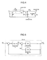
- FIG. 4 is a circuit block diagram in which the constant power load 80 of the circuit shown in FIG. 2 is replaced with a resistor 60. As shown in FIG. 4 , as a load viewed from the LC filter side, the resistor 60 having a resistance value R0 is connected in FIG. 4 .
- FIG. 5 is a block diagram of a transfer function of the circuit shown in FIG. 4 .
- the closed loop transfer function Gp(s) from the input voltage ES to the voltage EFC of the capacitor is represented by the following Formula (8):
- Gp s 1 C ⁇ L s 2 + 1 C ⁇ R ⁇ 0 + R L ⁇ s + 1 C ⁇ L ⁇ R R ⁇ 0 + 1
- the control circuit explained in this embodiment is devised with attention directed to this principle. Specifically, the control circuit controls the switching circuit 10 such that the constant power load 80 of the circuit shown in FIG. 2 has a characteristic equivalent to the positive resistance characteristic with respect to an oscillation component of the voltage EFC of the capacitor 6.
- electric power PR in the resistor 60 is represented by the following Formula (10):
- the electric power PRn in the resistor 60 is proportional to the square of a change rate of the voltage EFC of the capacitor 6. Therefore, the constant power load 80 is controlled such that the relation of Formula (11) holds. This makes it possible to cause the constant power load 80 to operate to have the positive resistance characteristic with respect to the fluctuation in the voltage EFC of the capacitor 6.
- the terminal voltage BFC of the power storage element 26 is a value that changes according to stored energy of the power storage element 26.
- the resonant frequency of the LC filter is usually 10 hertz to 20 hertz, which is equivalent to time of 50 milliseconds to 100 milliseconds in terms of a period.
- the terminal voltage BFC of the power storage element 26 can be regarded as fixed in time unit of several tens seconds. In other words, in considering electric oscillation at the resonant frequency of the LC filter, it can be assumed that the terminal voltage BFC of the power storage element 26 is fixed.
- the input power PDC of the switching circuit 10 can be changed in proportion to the square of the change rate of the voltage EFC of the capacitor 6.
- the constant power load 80 of the circuit shown in FIG. 2 has a characteristic equivalent to the positive resistance characteristic with respect to the electric oscillation of the voltage EFC of the capacitor 6 occurring at the resonant frequency of the LC filter.
- a value obtained by raising a fluctuation rate of the voltage EFC of the capacitor 6 to the second power is integrated with the smoothing reactor current command ISL*. This makes it possible to suppress the electric oscillation of the voltage EFC of the capacitor 6 occurring at the resonant frequency of the LC filter and stabilize the voltage EFC.
- FIG. 6 is a diagram of changes in state amounts on the inside of the damping control unit 40 and signal waveforms in the first embodiment.
- the damping control unit 40 includes a high-pass filter (hereinafter referred to as "HPF") 41, low-pass filters (hereinafter referred to as "LPFs”) 42 and 43, an adder 44, a divider 45, a subtracter 46, a switch 47, a square operator 48, and a limiter 49.
- HPF high-pass filter
- LPFs low-pass filters
- the voltage EFC of the capacitor 6 is input to the damping control unit 40 and is divided into two systems.
- the HPF 41 and the LPF 43 are connected to one system in series
- a resonant frequency component EFCa obtained by removing, with the HPF 41 and the LPF 43, an unnecessary low-frequency component and an unnecessary high-frequency component including a DC component of the voltage EFC of the capacitor 6 and extracting only a frequency component near the resonant frequency of the LC filter is output.
- EFCa is a signal that fluctuates in-phase with a resonant frequency component of EFC in a range of +150 volts to -150 volts.
- the LPF 42 is connected to the other system.
- a DC component EFCd obtained by extracting only a DC component of the voltage EFC of the capacitor 6 with the LPF 42 is output.
- the HPF 41, the LPF 42, and the LPF 43 are first order filters including first order lag elements. Explanation of the configuration of the HPF 41, the LPF 42, and the LPF 43 is omitted because the configuration is publicly known. It goes without saying that the HPF 41, the LPF 42, and the LPF 43 can include second or higher order filters. However, there is a disadvantage that the configuration of the filters becomes complicated.
- the LPF 43 is necessary to remove a high-frequency component, which is disturbance to the control system, included in the voltage EFC of the capacitor.
- a lower limit of the high-frequency component desired to be removed is several hundreds hertz and close to a resonant frequency band (usually, about 10 hertz to 20 hertz) of the LC filter, which is a target of damping control. Therefore, it is undesirable to remove the high-frequency component using only the LPF 43 because a phase delay of a resonant frequency component of the LC filter is caused.
- the HPF 41 is added in series and combined with the LPF 43 to compensate for a phase delay of a resonant frequency band of the LC filter while securing a high-frequency component removal characteristic same as that obtained when the LPF 43 is independently used.
- the adder 44 adds the DC component EFCd to the oscillation component EFCa of the resonant frequency band of the LC filter calculated as explained above and outputs EFCad.
- the divider 45 divides EFCad by the DC component EFCd to thereby calculate a fluctuation rate of the oscillation component of the resonant frequency band of the LC filter included in the voltage EFC of the capacitor 6 (hereinafter simply referred to as "fluctuation rate”) EFCfp.
- the fluctuation rate EFCfp is divided into two systems. One system is directly output to the switch 47 and the other system is output to the subtracter 46.
- the subtracter 46 subtracts the fluctuation rate EFCfp from a predetermined value (in the example of this embodiment, a value "2") and outputs EFCfn obtained by inverting a phase of an oscillation component of the fluctuation rate EFCfp to the switch 47.
- EFCfn When the power flow is in the direction from the power storage element 26 to the overhead wire 1 (the output side to the input side), EFCfn is used because the direction of the power flow is opposite to the direction from the overhead wire 1 to the power storage element 26 (the input side to the output side). In this case, operation in a direction for reducing the magnitude of electric power if the voltage EFC of the capacitor 6 increases and increasing the magnitude of electric power if the voltage EFC of the capacitor 6 decreases is necessary. Therefore, EFCfn obtained by inverting the phase of EFCfp is necessary.
- the square operator 48 raises EFCfp or EFCfn to the second power and outputs EFCfp or EFCfn to the limiter 49.
- the limiter 49 outputs, after limiting an upper limit and a lower limit of a signal output from the square operator 48 to arbitrary values according to necessity, the signal to the multiplier 34 as the damping operation amount DAMPCN.
- the limiter 49 has only to set an upper limit and a lower limit for amplitude limitation.
- the multiplier 34 integrates the damping operation amount DAMPCN with the smoothing reactor current command ISL* and generates a smoothing reactor current command ISL**.
- Smoothing reactor current control is carried out according to the smoothing reactor current command ISL** obtained as explained above. This makes it possible to suppress oscillation of the voltage EFC of the capacitor 6 and perform stable operation of the DCDC converter 100.
- the DCDC converter according to the first embodiment includes the damping control unit that automatically calculates, without gain adjustment and the like, an optimum damping operation amount for suppressing electric oscillation occurring in the input filter circuit.
- the DCDC converter controls the switching circuit based on the obtained damping operation amount. This makes it possible to suppress electric oscillation occurring in the LC input filter circuit and perform stable operation of the DCDC converter functioning as a control current source.
- the DCDC converter generates a smoothing reactor current command including the damping operation amount and controls the switching circuit based on the obtained smoothing reactor current command. Therefore, an electric current flowing to the smoothing reactor is optimally controlled to suppress electric oscillation of the input filter circuit and it is possible to perform stable operation.
- a fluctuation rate of the voltage of the input capacitor is calculated by dividing the voltage of the input capacitor by a DC component of the input capacitor. This makes it possible to perform control corresponding to the fluctuation rate of the voltage of the input capacitor.
- bands equal to or higher than a frequency near the resonant frequency of the LC filter are allowed to pass by the high-pass filter and bands equal to or lower than the frequency near the resonant frequency of the LC filter are allowed to pass by the low-pass filter. This makes it possible to cut an unnecessary high-frequency component, which is disturbance to the control system, without causing a phase delay near the resonant frequency of the LC filter.
- a fluctuation rate of the voltage of the input capacitor is raised to the second power to calculate a damping operation amount. This makes it possible to perform control of a smoothing reactor current matching the level of electric oscillation of the voltage of the input capacitor.
- an upper limit and a lower limit of a damping operation amount are limited at the final stage. This makes it possible to limit a transient fluctuation amount of a smoothing reactor current involved in, for example, the damping control.
- a constant of a circuit element of the DCDC converter is not used for calculation of the damping operation amount DAMPCN. Therefore, there is also an advantage that, even when the constant of the circuit element is changed, adjustment of the control system is unnecessary.
- the control system that suppresses electric oscillation occurring at the resonant frequency of the LC filter and enables stable operation is configured.
- a control system that suppresses electric oscillation occurring at the resonant frequency of the LC filter and enables stable operation is configured.
- FIG. 7 is a diagram of a configuration example of the DCDC converter in the second embodiment of the present invention.
- a DCDC converter 100a in the second embodiment includes a main circuit unit 200a and a control unit 300a that controls a power flow in the main circuit unit 200a.
- Components same as or equivalent to those in the first embodiment are denoted by the same reference numerals and signs and detailed explanation of the components is omitted.
- the power storage element 26 in the first embodiment is replaced with a load 24 and a smoothing capacitor 22 combined with the smoothing reactor 20 to configure a smoothing filter circuit 27a and a current detector 25 that detects an electric current flowing to the load 24 are provided at a post stage of the current detector 21 on the load 24 side of the switching circuit 10.
- the voltage of the load 24 is smoothed by a smoothing filter including the smoothing reactor 20 and the smoothing capacitor 22.
- a control-signal generating unit 50a includes, in addition to the components in the first embodiment, a subtracter 31, a voltage controller 32, and an adder 33 at a pre-stage of the multiplier 34.
- a smoothing capacitor voltage command BFC* as a command value of the voltage of the smoothing capacitor 22 is input to the control-signal generating unit 50a from a host control system (not shown).
- the DCDC converter 100a in the second embodiment operates as a control voltage source that controls the voltage of the load 24 to be a predetermined value according to the smoothing capacitor voltage command BFC* output from the host control system.
- the subtracter 31 subtracts a voltage BFC of the smoothing capacitor 22 from BFC* and outputs the BFC*.
- the voltage controller 32 is input with the output of the subtracter 31 and performs proportional integral control.
- the proportional integral control or proportional control is suitable. Because the voltage controller 32 can be configured by a publicly-known technology irrespective of which of the control systems is adopted, explanation of the control system is omitted here.
- the adder 33 adds up an output of the voltage controller 32 and a load current ILD and outputs the added-up output and the load current ILD to the multiplier 34 as the smoothing reactor current command ISL*.
- the multiplier 34 integrates the damping operation amount DAMPCN with the smoothing reactor current command ISL* output from the adder 33 and generates the smoothing reactor current command ISL**.
- Smoothing reactor current control is carried out according to the smoothing reactor current command ISL** obtained as explained above. Consequently, oscillation of the voltage EFC of the capacitor 6 is suppressed and it is possible to perform stable operation of the DCDC converter 100a.
- FIG. 8 is a diagram of another configuration example of the DCDC converter in the second embodiment of the present invention.
- the configuration of the main circuit unit 200a in a DCDC converter 100b is the same as that shown in FIG. 7 .
- a control-signal generating unit 50b of a control unit 300b is added with a multiplier 30 at a pre-stage of the subtracter 31 instead of the multiplier 34 at the post stage of the adder 33 shown in FIG. 7 and configured to multiply together a command value BFC* of the voltage of the smoothing capacitor 22 and the damping operation amount DAMPCN, generate a smoothing capacitor voltage command BFC**, and add the smoothing capacitor voltage command BFC** to the load current ILD with the adder 33 to thereby generate the smoothing reactor current command ISL**.
- Components other than those explained above are the same as the components shown in FIG. 7 .
- FIG. 7 there is an effect that oscillation of the voltage EFC of the capacitor 6 is suppressed and it is possible to perform stable operation of the DCDC converter 100b.
- the smoothing reactor current command ISL** is generated by using the load current ILD flowing to the load 24. This makes it possible to also suppress fluctuation in the voltage BFC of the smoothing capacitor 22.
- the DCDC converter according to the second embodiment includes the damping control unit that automatically calculates, without gain adjustment and the like, an optimum damping operation amount for suppressing electric oscillation occurring in the input filter circuit.
- the DCDC converter generates a smoothing reactor current command including the damping operation amount and controls the switching circuit based on the obtained smoothing reactor current command. This makes it possible to suppress electric oscillation occurring in the LC input filter circuit and perform stable operation of the DCDC converter functioning as the control voltage source.
- a constant of a circuit element of the DCDC converter is not used for calculation of the damping operation amount DAMPCN. Therefore, there is an advantage that, even when the constant of the circuit element is changed, adjustment of the control system is unnecessary.
- the configurations explained in the first and second embodiments are examples of the configuration of the present invention. It goes without saying that the configurations can be combined with another publicly-known technology or can be changed in such a manner, for example, that a part of the configurations is omitted without departing from the spirit of the present invention.
- the explanation of the invention content is carried out with the DCDC converter assumed to be applied to the electric railroad field set as a target.
- an application field is not limited to this. It goes without saying that the DCDC converter can be applied to various industrial application fields.
- the DCDC converter according to the present invention is used as an invention that suppresses electric oscillation occurring in an input filter circuit and enables stable operation.
Abstract
Description
- The present invention relates to a DCDC converter suitable for application to, for example, an electric motor car.
- In general, for the electric motor car, a configuration for collecting electric power from an overhead wire, a third rail, or the like with a current collector and driving a motor using the collected power is adopted.
- In recent years, because the performance of power storage elements such as a secondary battery and an electric double layer capacitor is improved, development of a system is underway in which the power storage elements are mounted on an electric motor car, collected electric power is stored in the power storage elements, and a motor is driven by using both the electric power stored in the power storage elements and electric power collected by a current collector.
- As such a system, for example, there is an electric motor car control apparatus disclosed in
Patent Document 1 described below. In this electric motor car control apparatus, to control power flow between an overhead wire and a power storage element, a DCDC converter is provided between the current collector and the power storage element. - Although not provided in the electric motor car control apparatus disclosed in
Patent Document 1, in the system of this type, a reactor is provided between the DCDC converter and the overhead wire and attenuation of a harmonic current output from the DCDC converter to the overhead wire side is performed by an LC filter circuit including this reactor and an input capacitor. - Patent Document: Japanese Patent Application Laid-open No.
2007-274756 - However, the inventor found that, when the DCDC converter is actuated, because, for example, electric oscillation occurs in the LC filter circuit and the input capacitor is subjected to overvoltage, in some case, normal operation of the DCDC converter cannot be performed.
- The present invention has been devised in view of the knowledge of the inventor and it is an object of the present invention to provide a DCDC converter that suppresses electric oscillation occurring in an LC filer circuit and enables stable operation.
- In order to solve the aforementioned problems and attain the aforementioned object, a DCDC converter according to one aspect of the present invention is constructed in such a manner as to have an input filter circuit including an input reactor connected to a DC power supply and an input capacitor and converts a DC voltage of the input capacitor into an arbitrary DC voltage to output the DC voltage, and further includes: a switching circuit, to an input end of which the input filer circuit is connected, the switching circuit including an upper arm side switching element and a lower arm side switching element; a smoothing filer circuit connected to an output end of the switching circuit; and a control unit that feeds back a state amount of the smoothing filter circuit and controls to turn on and off the switching circuit, wherein the control unit includes a damping control unit that calculates, based on a voltage of the input capacitor, a damping operation amount for adjusting a state amount of the smoothing filter circuit.
- According to the present invention, the switching circuit is controlled based on an optimum damping operation amount for controlling electric oscillation occurring in the input filter circuit. Therefore, there is an effect that it is possible to suppress the electric oscillation occurring in the LC input filter circuit and perform stable operation of the DCDC converter.
-
-
FIG. 1 is a diagram of a configuration example of a DCDC converter in a first embodiment. -
FIG. 2 is a circuit block diagram in which a main circuit unit shown inFIG. 1 is simplified. -
FIG. 3 is a block diagram of a transfer function of a circuit shown inFIG. 2 . -
FIG. 4 is a circuit block diagram in which a constant power load of the circuit shown inFIG. 2 is replaced with a resistor. -
FIG. 5 is a block diagram of a transfer function of a circuit shown inFIG. 4 . -
FIG. 6 is a diagram of changes in state amounts on the inside of a damping control unit and signal waveforms in the first embodiment. -
FIG. 7 is a diagram of a configuration example of a DCDC converter in a second embodiment. -
FIG. 8 is a diagram of another configuration example of the DCDC converter in the second embodiment. -
- 1
- Overhead wire
- 2
- Current collector
- 3
- Wheel
- 4
- Rail
- 5
- Reactor
- 6
- Capacitor
- 7
- Voltage detector
- 8
- Input filter circuit
- 10
- Switching circuit
- 11
- Upper arm side switching element
- 12
- Lower arm side switching element
- 20
- Smoothing reactor
- 21
- Current detector
- 22
- Smoothing capacitor
- 23
- Voltage detector
- 24
- Load
- 25
- Current detector
- 26
- Power storage element
- 27,
- 27a Smoothing filter circuits
- 30
- Multiplier
- 31
- Subtracter
- 32
- Voltage controller
- 33
- Adder
- 34
- Multiplier
- 35
- Subtracter
- 36
- Current controller
- 37
- Modulation circuit
- 40
- Damping control unit
- 41
- HPF (high-pass filter)
- 42, 43
- LPFs (low-pass filters)
- 44
- Adder
- 45
- Divider
- 46
- Subtracter
- 47
- Switch
- 48
- Square operator
- 49
- Limiter
- 50,
- 50a Control-signal generating units
- 60
- Resistor
- 70
- DC power supply
- 80
- Constant power load
- 100,
- 100a, 100b DCDC converters
- 200, 200a
- Main circuit units
- 300, 300a, 300b
- Control units
- Embodiments of a DCDC converter according to the present invention are explained in detail below based on the drawings. The present invention is not limited by the embodiments explained below.
-
FIG. 1 is a diagram of a configuration example of a DCDC converter in a first embodiment of the present invention. As shown inFIG. 1 , aDCDC converter 100 is electrically connected to anoverhead wire 1, which is connected to a substation (not shown) serving as a DC power supply, via acurrent collector 2. TheDCDC converter 100 is also electrically connected to arail 4, which is connected to the substation, via awheel 3 serving as a return circuit for a return current. - The
DCDC converter 100 includes amain circuit unit 200 and acontrol unit 300 that controls a power flow in themain circuit unit 200. - First, the configuration of the
main circuit unit 200 is explained. InFIG. 1 , themain circuit unit 200 includes, as main components, aninput filter circuit 8, a voltage detector 7, a switchingcircuit 10, a smoothingfilter circuit 27, avoltage detector 23, acurrent detector 21, and apower storage element 26. The switchingcircuit 10 includes an upper armside switching element 11 and a lower armside switching element 12. Theinput filter circuit 8 includes areactor 5 as an input reactor and acapacitor 6 as an input capacitor. The smoothingfilter circuit 27 includes a smoothingreactor 20. - Schematic functions of the units included in the
main circuit unit 200 are explained. The switchingcircuit 10 functions as a power converting circuit in two directions from theoverhead wire 1 to thepower storage element 26 and from thepower storage element 26 to theoverhead wire 1. Theinput filter circuit 8 suppresses a harmonic current generated from the switchingcircuit 10 from flowing out to the substation side via thecurrent collector 2. The voltage detector 7 detects a voltage EFC at both ends of thecapacitor 6. Thepower storage element 26 accumulates required electric power. Thevoltage detector 23 detects a terminal voltage BFC of thepower storage element 26. The smoothingfilter circuit 27 performs filtering of a current ripple generated from the switchingcircuit 10. Thecurrent detector 21 detects an electric current flowing to the smoothing reactor 20 (hereinafter referred to as "smoothing reactor current") ISL. - A connection configuration of the
main circuit unit 200 is explained. An output side of the switchingcircuit 10 is connected to thepower storage element 26 via the smoothingreactor 20 and thecurrent detector 21 with a connection end between the upper armside switching element 11 and the lower arm side switching element 12 (one end of the upper arm side switching element 11) used as an output end. An input side of the switchingcircuit 10 is connected to theoverhead wire 1 via theinput filter circuit 8 and thecurrent collector 2 with the other end of the upper armside switching element 11 used as an input end. - As the
power storage element 26, a nickel hydrogen secondary battery, a lithium ion secondary battery, an electric double layer capacitor, or the like is suitable. However, other power storage elements can be used. As the DC power supply that supplies electric power to theoverhead wire 1, the substation is explained as an example. However, the DC power supply can be other DC power supply. - The configuration and the function of the
control unit 300 are explained. Thecontrol unit 300 includes a control-signal generating unit 50 and a dampingcontrol unit 40. The control-signal generating unit 50 includes amultiplier 34, asubtracter 35, acurrent controller 36, amodulation circuit 37, and a dampingcontrol unit 40. - The
multiplier 34 performs multiplication of a smoothing reactor current command ISL* input from a host control system (not shown) and a damping operation amount DAMPCN explained later. The smoothing reactor current command ISL* is a command value of the smoothing reactor current ISL. - The
subtracter 35 subtracts the smoothing reactor current ISL from an output (ISL**) of themultiplier 34. - The
current controller 36 is input with an output of thesubtracter 35 and performs proportional integral control. As a control system of thecurrent controller 36, the proportional integral control is suitable. However, the control system can be proportional control. Thecurrent controller 36 can be configured by a publicly-known technology irrespective of which of the control systems is adopted. Therefore, explanation of the control system is omitted here. - The
modulation circuit 37 outputs, based on an output of thecurrent controller 36, the voltage EFC of thecapacitor 6, and the terminal voltage BFC of thepower storage element 26, a control signal to the switching circuit 10 (hereinafter referred to as "switching signal") GSG. - The damping
control unit 40 is input with the voltage EFC of thecapacitor 6 and outputs the damping operation amount DAMPCN. The configuration of the dampingcontrol unit 40 is explained later together with the operation thereof. - Power flow control of the
main circuit unit 200 by thecontrol unit 300 configured as above is explained. - The smoothing reactor current command ISL* is the command value of the smoothing reactor current ISL output from the host control system (not shown) as explained above. When charge and discharge of the
power storage element 26 are unnecessary, ISL* is set to 0 and thecontrol unit 300 controls the switchingcircuit 10 of themain circuit unit 200 such that the smoothing reactor current ISL does not flow. - When charge of the
power storage element 26 is necessary, ISL* is set to a positive value and thecontrol unit 300 controls the switchingcircuit 10 of themain circuit unit 200 to perform a charge operation such that the smoothing reactor current ISL changes to a power flow from theoverhead wire 1 side to thepower storage element 26 side. - When discharge of the
power storage element 26 is necessary, ISL* is set to a negative value and thecontrol unit 300 controls the switchingcircuit 10 of themain circuit unit 200 to perform a discharge operation such that the smoothing reactor current ISL changes to a power flow from thepower storage element 26 side to theoverhead wire 1 side. - In short, the
DCDC converter 100 functions as a control current source that controls, according to the smoothing reactor current command ISL* output from the host control system, the smoothing reactor current ISL to be a predetermined value and is capable of realizing an arbitrary power flow corresponding to necessity. - The damping
control unit 40 as a main part of this embodiment is explained. - Before specific explanation of the damping
control unit 40 shown inFIG. 1 , a cause of occurrence of electric oscillation in an LC filter including the input filter circuit 8 (thereactor 5 and the capacitor 6) of themain circuit unit 200 shown inFIG. 1 and a principle of suppression of electric oscillation as a ground for the configuration of the dampingcontrol unit 40 are briefly explained with reference to drawings ofFIGS. 1 to 5 . - First, the cause of occurrence of electric oscillation in the LC filter of the
main circuit unit 200 shown inFIG. 1 is explained.FIG. 2 is a circuit block diagram in which themain circuit unit 200 shown inFIG. 1 is simplified. InFIG. 2 , theoverhead wire 1, thecurrent collector 2, thewheel 3, and therail 4 inFIG. 1 are not shown and the substation is replaced with aDC power supply 70. Thereactor 5 includes an inductance component L and a resistance component R. The capacitance of thecapacitor 6 is represented as C. - The switching
circuit 10 is controlled such that the smoothing reactor current ISL is maintained constant even if the voltage EFC of thecapacitor 6 fluctuates. In other words, even if the voltage EFC of thecapacitor 6 fluctuates, because input power PDC of the switchingcircuit 10 is controlled not to change, the switchingcircuit 10 has a constant power characteristic with respect to the fluctuation in the voltage EFC of thecapacitor 6. Therefore, blocks including the switchingcircuit 10, the smoothingreactor 20, and thepower storage element 26 are collected as one load viewed from the LC filer side and set as aconstant power load 80. - In
FIG. 2 , theconstant power load 80 has a negative resistance characteristic that, if the voltage EFC of thecapacitor 6 rises, an input current IDC of the switchingcircuit 10 decreases and, if the voltage EFC of thecapacitor 6 falls, the input current IDC of the switchingcircuit 10 increases. A normal resistor (a positive resistor) has a positive resistance characteristic that, if a voltage rises, an electric current increases and, if the voltage falls, the electric current decreases. In other words, theconstant power load 80 has a characteristic opposite to that of the normal resistor in a change of an electric current with respect to a change in a voltage. - Therefore, if the voltage EFC of the
capacitor 6 rises and the input current IDC of the switchingcircuit 10 decreases, the circuit shown inFIG. 2 operates to facilitate the rise in the voltage EFC of thecapacitor 6. Conversely, if the voltage EFC of thecapacitor 6 falls and the input current IDC of the switchingcircuit 10 increases, the circuit operates to facilitate the fall in the voltage EFC of thecapacitor 6. Therefore, in the circuit shown inFIG. 2 , damping is not effective on the fluctuation in the voltage EFC of thecapacitor 6, electric oscillation of the voltage EFC of thecapacitor 6 occurs at a resonant frequency of the LC filter, the amplitude of the occurred electric oscillation expands, and the voltage EFC continues to oscillate. The above is qualitative explanation of the cause of occurrence of the electric oscillation in the LC filters of themain circuit unit 200 shown inFIG. 1 and the circuit shown inFIG. 2 . - A transfer function of the circuit shown in
FIG. 2 is calculated and evaluated and quantitative explanation of the phenomenon qualitatively explained above is made. - First, a relational expression of the input power PDC of the switching
circuit 10, the input current IDC of the switchingcircuit 10, and the voltage EFC of thecapacitor 6 is the following Formula (1): -

- Because Formula (1) is nonlinear, Formula (1) is linearized. When a voltage and an electric current at an operating point are respectively represented as EFC0 and IDC0, the following Formula (2) holds near the operating point:
-

- Therefore, the circuit shown in
FIG. 2 is represented by a block diagram shown inFIG. 3. FIG. 3 is a block diagram of a transfer function of the circuit shown inFIG. 2 . In the transfer function block diagram shown inFIG. 3 , a closed loop transfer function G(s) from an input voltage ES to the voltage EFC of thecapacitor 6 is represented by the following Formula (3): -

- A condition for stabilizing a closed loop system shown in the closed loop transfer function G(s) of Formula (3) is that all poles of G(s) are negative. In other words, all solutions of a characteristic equation indicated by the following Formula (4), which is the denominator of G(s), need to be negative.
-

- When solutions of Formula (4) are represented as α and β, conditional expressions for making both α and β negative are the following Formulas (5) and (6) from a relation between the solutions and coefficients:
-

-

- A conditional expression of the resistance component R of the
reactor 5 for stabilizing the closed loop system indicated by the transfer function G(s) of Formula (3) is calculated. Attention is directed to Formula (5) because Formula (6) does not include useful information. When Formula (5) is modified, the following Formula (7) as the conditional expression of the resistance component R of thereactor 5 is obtained. -

- According to Formula (7), R necessary for stabilizing the system can be smaller as L is smaller, C is larger, PDC is smaller, and EFC0 is larger. As an example, when conditions L=12 mH, C=6600 µF, PDC=1000 KW, and EFC0=1500 V, which are general numerical values, are substituted in Formula (7), a value of the resistance component R of the
reactor 5 that can stabilize the closed loop system indicated by the transfer function G(s) of Formula (3) is R>0.8 (Ω). - In general, a resistance component included in a reactor is very small at about several tens (mΩ) and it is impossible to satisfy Formula (7). Therefore, the closed loop system of the circuit shown in
FIG. 2 is unstable and electric oscillation occurs at a resonant frequency of the LC filter. In other words, it can be understood that, unless a resistor that satisfies Formula (7) is added to the circuit shown inFIG. 2 or stabilization of the closed loop system is realized in terms of control, the voltage EFC of thecapacitor 6 oscillates and diverges. Actually, the addition of the resistor increases the size of an apparatus and causes an increase in a loss. Therefore, another method of realizing the stabilization in terms of control is necessary. - The above is the quantitative explanation of the cause of occurrence of the electric oscillation at the resonant frequency of the LC filters of the
main circuit unit 200 shown inFIG. 1 and of the circuit shown inFIG. 2 . - The principle of suppression of electric oscillation as a technical ground for the configuration of the damping
control unit 40 according to this embodiment is explained. - As explained above, the
constant power load 80 of the circuit shown inFIG. 2 has the negative resistance characteristic. If this constant power load has a positive resistance characteristic, it is possible to stabilize the closed loop. Therefore, quantitative explanation same as above is made using a circuit diagram in which theconstant power load 80 of the circuit shown inFIG. 2 is replaced with a resistor. -
FIG. 4 is a circuit block diagram in which theconstant power load 80 of the circuit shown inFIG. 2 is replaced with aresistor 60. As shown inFIG. 4 , as a load viewed from the LC filter side, theresistor 60 having a resistance value R0 is connected inFIG. 4 . -
FIG. 5 is a block diagram of a transfer function of the circuit shown inFIG. 4 . According to the transfer function block diagram shown inFIG. 5 , the closed loop transfer function Gp(s) from the input voltage ES to the voltage EFC of the capacitor is represented by the following Formula (8): -

- A characteristic equation of the closed loop transfer function Gp(s) indicated by Expression (8) is the following Formula (9):
-

- When a condition for making all solutions of the characteristic equation indicated by Formula (9) negative is calculated, a value of the resistance component R of the
reactor 5 is R≥0 and this condition is always satisfied. In other words, it is seen that, as shown inFIG. 4 , when the load viewed from the LC filer side includes theresistor 60, the closed loop system is always stable. - As explained above, it is seen that the circuit in which the
resistor 60 is connected to the LC filter connected to theDC power supply 70 is always stable. The control circuit explained in this embodiment is devised with attention directed to this principle. Specifically, the control circuit controls the switchingcircuit 10 such that theconstant power load 80 of the circuit shown inFIG. 2 has a characteristic equivalent to the positive resistance characteristic with respect to an oscillation component of the voltage EFC of thecapacitor 6. - Subsequently, a control condition for the
constant power load 80 of the circuit shown inFIG. 2 to have the characteristic equivalent to the positive resistance characteristic with respect to electric oscillation of the voltage EFC of thecapacitor 6 occurring at the resonant frequency of the LC filter is derived. - In
FIG. 4 , when the voltage of thecapacitor 6 is EFC and the electric current flowing to theresistor 60 is IDC, electric power PR in theresistor 60 is represented by the following Formula (10): -

- When the voltage EFC of the
capacitor 6 fluctuates and increases to n times an initial voltage, the electric current IDC flowing to theresistor 60 also increases to n times an initial electric current. Therefore, electric power PRn in theresistor 60 at this point is represented by the following Formula (11): -

- In other words, the electric power PRn in the
resistor 60 is proportional to the square of a change rate of the voltage EFC of thecapacitor 6. Therefore, theconstant power load 80 is controlled such that the relation of Formula (11) holds. This makes it possible to cause theconstant power load 80 to operate to have the positive resistance characteristic with respect to the fluctuation in the voltage EFC of thecapacitor 6. - On the other hand, in
FIG. 2 , when a circuit loss of the switchingcircuit 10 is neglected, the output power of the switchingcircuit 10 is equal to the input power PDC of the switchingcircuit 10. Therefore, the following Formula (12) holds from the smoothing reactor current ISL flowing in thepower storage element 26 and the terminal voltage BFC of the power storage element 26: -

- The terminal voltage BFC of the
power storage element 26 is a value that changes according to stored energy of thepower storage element 26. - To cause the
constant power load 80 to operate to have the positive resistance characteristic with respect to the fluctuation in the voltage EFC of thecapacitor 6, electric power PDCn at the time when the voltage EFC of thecapacitor 6 increases to n times has only to satisfy a relation of the following Formula (13) in the same manner as Formula (11): -

- The resonant frequency of the LC filter is usually 10 hertz to 20 hertz, which is equivalent to time of 50 milliseconds to 100 milliseconds in terms of a period. On the other hand, the terminal voltage BFC of the
power storage element 26 can be regarded as fixed in time unit of several tens seconds. In other words, in considering electric oscillation at the resonant frequency of the LC filter, it can be assumed that the terminal voltage BFC of thepower storage element 26 is fixed. - Therefore, when the voltage EFC of the
capacitor 6 increases to n times, if the switchingcircuit 10 is controlled to multiply the smoothing reactor current ISL by n2, the input power PDC of the switchingcircuit 10 can be changed in proportion to the square of the change rate of the voltage EFC of thecapacitor 6. Theconstant power load 80 of the circuit shown inFIG. 2 has a characteristic equivalent to the positive resistance characteristic with respect to the electric oscillation of the voltage EFC of thecapacitor 6 occurring at the resonant frequency of the LC filter. - Therefore, in the
control unit 300 shown inFIG. 1 , a value obtained by raising a fluctuation rate of the voltage EFC of thecapacitor 6 to the second power is integrated with the smoothing reactor current command ISL*. This makes it possible to suppress the electric oscillation of the voltage EFC of thecapacitor 6 occurring at the resonant frequency of the LC filter and stabilize the voltage EFC. - A specific configuration for embodying the control method explained above is explained with reference to
FIGS. 1 and6. FIG. 6 is a diagram of changes in state amounts on the inside of the dampingcontrol unit 40 and signal waveforms in the first embodiment. - First, the configuration of the damping
control unit 40 is explained with reference toFIG. 1 . The dampingcontrol unit 40 includes a high-pass filter (hereinafter referred to as "HPF") 41, low-pass filters (hereinafter referred to as "LPFs") 42 and 43, anadder 44, adivider 45, asubtracter 46, aswitch 47, asquare operator 48, and alimiter 49. - The voltage EFC of the
capacitor 6 is input to the dampingcontrol unit 40 and is divided into two systems. - The
HPF 41 and theLPF 43 are connected to one system in series A resonant frequency component EFCa obtained by removing, with theHPF 41 and theLPF 43, an unnecessary low-frequency component and an unnecessary high-frequency component including a DC component of the voltage EFC of thecapacitor 6 and extracting only a frequency component near the resonant frequency of the LC filter is output. For example, as shown inFIG. 6 , when the voltage EFC of thecapacitor 6 oscillates up to 1650 volts to 1350 volts with 1500 volts in the center, EFCa is a signal that fluctuates in-phase with a resonant frequency component of EFC in a range of +150 volts to -150 volts. - The
LPF 42 is connected to the other system. A DC component EFCd obtained by extracting only a DC component of the voltage EFC of thecapacitor 6 with theLPF 42 is output. - The
HPF 41, theLPF 42, and theLPF 43 are first order filters including first order lag elements. Explanation of the configuration of theHPF 41, theLPF 42, and theLPF 43 is omitted because the configuration is publicly known. It goes without saying that theHPF 41, theLPF 42, and theLPF 43 can include second or higher order filters. However, there is a disadvantage that the configuration of the filters becomes complicated. - Actions of the
HPF 41 and theLPF 43 are explained more in detail. - The
LPF 43 is necessary to remove a high-frequency component, which is disturbance to the control system, included in the voltage EFC of the capacitor. However, a lower limit of the high-frequency component desired to be removed is several hundreds hertz and close to a resonant frequency band (usually, about 10 hertz to 20 hertz) of the LC filter, which is a target of damping control. Therefore, it is undesirable to remove the high-frequency component using only theLPF 43 because a phase delay of a resonant frequency component of the LC filter is caused. Therefore, theHPF 41 is added in series and combined with theLPF 43 to compensate for a phase delay of a resonant frequency band of the LC filter while securing a high-frequency component removal characteristic same as that obtained when theLPF 43 is independently used. Concerning characteristics of theHPF 41 and theLPF 43, it is desirable to adjust a frequency with a gain of 1 to the resonant frequency (10 hertz to 20 hertz) of the LC filter. - The
adder 44 adds the DC component EFCd to the oscillation component EFCa of the resonant frequency band of the LC filter calculated as explained above and outputs EFCad. - The
divider 45 divides EFCad by the DC component EFCd to thereby calculate a fluctuation rate of the oscillation component of the resonant frequency band of the LC filter included in the voltage EFC of the capacitor 6 (hereinafter simply referred to as "fluctuation rate") EFCfp. - The fluctuation rate EFCfp is divided into two systems. One system is directly output to the
switch 47 and the other system is output to thesubtracter 46. Thesubtracter 46 subtracts the fluctuation rate EFCfp from a predetermined value (in the example of this embodiment, a value "2") and outputs EFCfn obtained by inverting a phase of an oscillation component of the fluctuation rate EFCfp to theswitch 47. - When a power flow is in a direction from the
overhead wire 1 side to thepower storage element 26 side, a contact on an upper side (a charge side) of theswitch 47 is selected and the fluctuation rate EFCfp is input to thesquare operator 48. - On the other hand, when the power flow is in a direction from the
power storage element 26 side to theoverhead wire 1 side, a contact on a lower side (a discharge side) of theswitch 47 is selected and the fluctuation rate EFCfn is input to thesquare operator 48. - When the power flow is in the direction from the
power storage element 26 to the overhead wire 1 (the output side to the input side), EFCfn is used because the direction of the power flow is opposite to the direction from theoverhead wire 1 to the power storage element 26 (the input side to the output side). In this case, operation in a direction for reducing the magnitude of electric power if the voltage EFC of thecapacitor 6 increases and increasing the magnitude of electric power if the voltage EFC of thecapacitor 6 decreases is necessary. Therefore, EFCfn obtained by inverting the phase of EFCfp is necessary. - The
square operator 48 raises EFCfp or EFCfn to the second power and outputs EFCfp or EFCfn to thelimiter 49. Thelimiter 49 outputs, after limiting an upper limit and a lower limit of a signal output from thesquare operator 48 to arbitrary values according to necessity, the signal to themultiplier 34 as the damping operation amount DAMPCN. In other words, when it is desired to limit a transient fluctuation amount of the smoothing reactor current ISL involved in, for example, damping control, thelimiter 49 has only to set an upper limit and a lower limit for amplitude limitation. - Finally, the
multiplier 34 integrates the damping operation amount DAMPCN with the smoothing reactor current command ISL* and generates a smoothing reactor current command ISL**. - Smoothing reactor current control is carried out according to the smoothing reactor current command ISL** obtained as explained above. This makes it possible to suppress oscillation of the voltage EFC of the
capacitor 6 and perform stable operation of theDCDC converter 100. - As explained above, the DCDC converter according to the first embodiment includes the damping control unit that automatically calculates, without gain adjustment and the like, an optimum damping operation amount for suppressing electric oscillation occurring in the input filter circuit. The DCDC converter controls the switching circuit based on the obtained damping operation amount. This makes it possible to suppress electric oscillation occurring in the LC input filter circuit and perform stable operation of the DCDC converter functioning as a control current source.
- The DCDC converter generates a smoothing reactor current command including the damping operation amount and controls the switching circuit based on the obtained smoothing reactor current command. Therefore, an electric current flowing to the smoothing reactor is optimally controlled to suppress electric oscillation of the input filter circuit and it is possible to perform stable operation.
- In the configuration of the damping control unit, a fluctuation rate of the voltage of the input capacitor is calculated by dividing the voltage of the input capacitor by a DC component of the input capacitor. This makes it possible to perform control corresponding to the fluctuation rate of the voltage of the input capacitor.
- In the configuration of the damping control unit, bands equal to or higher than a frequency near the resonant frequency of the LC filter are allowed to pass by the high-pass filter and bands equal to or lower than the frequency near the resonant frequency of the LC filter are allowed to pass by the low-pass filter. This makes it possible to cut an unnecessary high-frequency component, which is disturbance to the control system, without causing a phase delay near the resonant frequency of the LC filter.
- In the configuration of the damping control unit, a fluctuation rate of the voltage of the input capacitor is raised to the second power to calculate a damping operation amount. This makes it possible to perform control of a smoothing reactor current matching the level of electric oscillation of the voltage of the input capacitor.
- In the configuration of the damping control unit, an upper limit and a lower limit of a damping operation amount are limited at the final stage. This makes it possible to limit a transient fluctuation amount of a smoothing reactor current involved in, for example, the damping control.
- Further, a constant of a circuit element of the DCDC converter is not used for calculation of the damping operation amount DAMPCN. Therefore, there is also an advantage that, even when the constant of the circuit element is changed, adjustment of the control system is unnecessary.
- In the first embodiment, in the DCDC converter configured to function as the control current source that controls the smoothing reactor current ISL flowing in the power storage element to be a predetermined value, the control system that suppresses electric oscillation occurring at the resonant frequency of the LC filter and enables stable operation is configured. However, in a second embodiment, in a DCDC converter configured to replace the power storage element with a load and operate as a control voltage source that controls the voltage of the load to be a predetermined value, a control system that suppresses electric oscillation occurring at the resonant frequency of the LC filter and enables stable operation is configured.
-
FIG. 7 is a diagram of a configuration example of the DCDC converter in the second embodiment of the present invention. As shown inFIG. 7 , aDCDC converter 100a in the second embodiment includes amain circuit unit 200a and acontrol unit 300a that controls a power flow in themain circuit unit 200a. Components same as or equivalent to those in the first embodiment are denoted by the same reference numerals and signs and detailed explanation of the components is omitted. - In the
main circuit unit 200a, thepower storage element 26 in the first embodiment is replaced with aload 24 and a smoothingcapacitor 22 combined with the smoothingreactor 20 to configure a smoothingfilter circuit 27a and acurrent detector 25 that detects an electric current flowing to theload 24 are provided at a post stage of thecurrent detector 21 on theload 24 side of the switchingcircuit 10. The voltage of theload 24 is smoothed by a smoothing filter including the smoothingreactor 20 and the smoothingcapacitor 22. - A control-
signal generating unit 50a includes, in addition to the components in the first embodiment, asubtracter 31, avoltage controller 32, and anadder 33 at a pre-stage of themultiplier 34. - A smoothing capacitor voltage command BFC* as a command value of the voltage of the smoothing
capacitor 22 is input to the control-signal generating unit 50a from a host control system (not shown). In other words, theDCDC converter 100a in the second embodiment operates as a control voltage source that controls the voltage of theload 24 to be a predetermined value according to the smoothing capacitor voltage command BFC* output from the host control system. - The
subtracter 31 subtracts a voltage BFC of the smoothingcapacitor 22 from BFC* and outputs the BFC*. Thevoltage controller 32 is input with the output of thesubtracter 31 and performs proportional integral control. As a control system of thevoltage controller 32, the proportional integral control or proportional control is suitable. Because thevoltage controller 32 can be configured by a publicly-known technology irrespective of which of the control systems is adopted, explanation of the control system is omitted here. - The
adder 33 adds up an output of thevoltage controller 32 and a load current ILD and outputs the added-up output and the load current ILD to themultiplier 34 as the smoothing reactor current command ISL*. - The
multiplier 34 integrates the damping operation amount DAMPCN with the smoothing reactor current command ISL* output from theadder 33 and generates the smoothing reactor current command ISL**. - Smoothing reactor current control is carried out according to the smoothing reactor current command ISL** obtained as explained above. Consequently, oscillation of the voltage EFC of the
capacitor 6 is suppressed and it is possible to perform stable operation of theDCDC converter 100a. - Even when the DCDC converter is configured as shown in
FIG. 8 , it is possible to perform control same as that performed by the configuration shown inFIG. 7 .FIG. 8 is a diagram of another configuration example of the DCDC converter in the second embodiment of the present invention. - As shown in
FIG. 8 , the configuration of themain circuit unit 200a in aDCDC converter 100b is the same as that shown inFIG. 7 . A control-signal generating unit 50b of acontrol unit 300b is added with amultiplier 30 at a pre-stage of thesubtracter 31 instead of themultiplier 34 at the post stage of theadder 33 shown inFIG. 7 and configured to multiply together a command value BFC* of the voltage of the smoothingcapacitor 22 and the damping operation amount DAMPCN, generate a smoothing capacitor voltage command BFC**, and add the smoothing capacitor voltage command BFC** to the load current ILD with theadder 33 to thereby generate the smoothing reactor current command ISL**. Components other than those explained above are the same as the components shown inFIG. 7 . As inFIG. 7 , there is an effect that oscillation of the voltage EFC of thecapacitor 6 is suppressed and it is possible to perform stable operation of theDCDC converter 100b. - In the configurations shown in
FIGS. 7 and8 , the smoothing reactor current command ISL** is generated by using the load current ILD flowing to theload 24. This makes it possible to also suppress fluctuation in the voltage BFC of the smoothingcapacitor 22. - As explained above, the DCDC converter according to the second embodiment includes the damping control unit that automatically calculates, without gain adjustment and the like, an optimum damping operation amount for suppressing electric oscillation occurring in the input filter circuit. The DCDC converter generates a smoothing reactor current command including the damping operation amount and controls the switching circuit based on the obtained smoothing reactor current command. This makes it possible to suppress electric oscillation occurring in the LC input filter circuit and perform stable operation of the DCDC converter functioning as the control voltage source.
- A constant of a circuit element of the DCDC converter is not used for calculation of the damping operation amount DAMPCN. Therefore, there is an advantage that, even when the constant of the circuit element is changed, adjustment of the control system is unnecessary.
- The configurations explained in the first and second embodiments are examples of the configuration of the present invention. It goes without saying that the configurations can be combined with another publicly-known technology or can be changed in such a manner, for example, that a part of the configurations is omitted without departing from the spirit of the present invention.
- Further, in the embodiments, the explanation of the invention content is carried out with the DCDC converter assumed to be applied to the electric railroad field set as a target. However, an application field is not limited to this. It goes without saying that the DCDC converter can be applied to various industrial application fields.
- As explained above, the DCDC converter according to the present invention is used as an invention that suppresses electric oscillation occurring in an input filter circuit and enables stable operation.
Claims (17)
- A DCDC converter that has an input filter circuit including an input reactor connected to a DC power supply and an input capacitor and converts a DC voltage of the input capacitor into an arbitrary DC voltage to output the DC voltage, the DCDC converter comprising:a switching circuit, to an input end of which the input filer circuit is connected, the switching circuit including an upper arm side switching element and a lower arm side switching element;a smoothing filer circuit connected to an output end of the switching circuit; anda control unit that feeds back a state amount of the smoothing filter circuit and controls to turn on and off the switching circuit, whereinthe control unit includes a damping control unit that calculates, based on a voltage of the input capacitor, a damping operation amount for adjusting a state amount of the smoothing filter circuit.
- The DCDC converter according to claim 1, wherein, when the DCDC converter has a smoothing reactor, one end of which is connected to the output end of the switching circuit, as the smoothing filter circuit, the state amount of the smoothing filter circuit is an electric current flowing to the smoothing reactor.
- The DCDC converter according to claim 2, wherein the control unit generates a smoothing reactor current command reflecting the damping operation amount and controls to turn on and off the switching circuit based on the smoothing reactor current command.
- The DCDC converter according to claim 2, wherein the damping control unit divides the voltage of the input capacitor by a DC component of the voltage of the input capacitor to thereby calculate a fluctuation rate of the voltage of the input capacitor and calculate a damping operation amount corresponding to the fluctuation rate.
- The DCDC converter according to claim 2, wherein the damping control unit divides an added-up signal of a signal obtained by removing an unnecessary high-frequency component included in the voltage of the input capacitor from the voltage of the input capacitor and a DC component of the voltage of the input capacitor by the DC component to thereby calculate a fluctuation rate of the voltage of the input capacitor and calculate a damping operation amount corresponding to the fluctuation rate.
- The DCDC converter according to claim 2, wherein the damping operation amount is calculated by raising a fluctuation rate of the voltage of the input capacitor to a second power.
- The DCDC converter according to claim 2, wherein
when a power flow is in a direction from an input side to an output side of the switching circuit, the damping control unit calculates, as the damping operation amount, a signal obtained by raising a fluctuation rate of the voltage of the input capacitor to a second power and,
when the power flow is in a direction from the output side to the input side of the switching circuit, the damping control unit calculates, as the damping operation amount, a signal obtained by inverting a phase of the signal obtained by raising the fluctuation rate of the voltage of the input capacitor to the second power. - The DCDC converter according to any one of claims 3 to 7, wherein the damping control unit limits upper and lower limits of the damping operation amount with a limiter and outputs the damping operation amount.
- The DCDC converter according to claim 1, wherein, when the DCDC converter has, as the smoothing filter circuit, a smoothing reactor, one end of which is connected to the output end of the switching circuit, and a smoothing capacitor connected to the other end of the smoothing reactor, the state amount of the smoothing filter circuit is an electric current of the smoothing reactor or a voltage of the smoothing capacitor.
- The DCDC converter according to claim 9, wherein the control unit generates a smoothing reactor current command reflecting the damping operation amount and controls to turn on and off the switching circuit based on the smoothing reactor current command.
- The DCDC converter according to claim 9, wherein the control unit generates a smoothing capacitor voltage command reflecting the damping operation amount, generates a smoothing reactor current command based on the smoothing capacitor voltage command, and controls to turn on and off the switching circuit based on the smoothing reactor current command.
- The DCDC converter according to claim 9, wherein the damping control unit divides the voltage of the input capacitor by a DC component of the voltage of the input capacitor to thereby calculate a fluctuation rate of the voltage of the input capacitor and calculate a damping operation amount corresponding to the fluctuation rate.
- The DCDC converter according to claim 9, wherein the damping control unit divides an added-up signal of a signal obtained by removing an unnecessary high-frequency component included in the voltage of the input capacitor from the voltage of the input capacitor and a DC component of the voltage of the input capacitor by the DC component to thereby calculate a fluctuation rate of the voltage of the input capacitor and calculate a damping operation amount corresponding to the fluctuation rate.
- The DCDC converter according to claim 9, wherein the damping operation amount is calculated by raising a fluctuation rate of the voltage of the input capacitor to a second power.
- The DCDC converter according to claim 7, wherein
when a power flow is in a direction from an input side to an output side of the switching circuit, the damping control unit calculates, as the damping operation amount, a signal obtained by raising a fluctuation rate of the voltage of the input capacitor to a second power and,
when the power flow is in a direction from the output side to the input side of the switching circuit, the damping control unit calculates, as the damping operation amount, a signal obtained by inverting a phase of the signal obtained by raising the fluctuation rate of the voltage of the input capacitor to the second power. - The DCDC converter according to any one of claims 10 to 15, wherein the damping control unit limits upper and lower limits of the damping operation amount with a limiter and outputs the damping operation amount.
- The DCDC converter according to any one of claims 9 to 16 further comprising an electric current detecting unit that detects a load current flowing to a load connected to the smoothing capacitor, and the smoothing reactor current command is calculated in view of the load current.
Applications Claiming Priority (1)
| Application Number | Priority Date | Filing Date | Title |
|---|---|---|---|
| PCT/JP2008/067025 WO2010032316A1 (en) | 2008-09-19 | 2008-09-19 | Dc-dc converter |
Publications (3)
| Publication Number | Publication Date |
|---|---|
| EP2348622A1 true EP2348622A1 (en) | 2011-07-27 |
| EP2348622A4 EP2348622A4 (en) | 2014-10-29 |
| EP2348622B1 EP2348622B1 (en) | 2017-10-25 |
Family
ID=41393477
Family Applications (1)
| Application Number | Title | Priority Date | Filing Date |
|---|---|---|---|
| EP08811042.4A Active EP2348622B1 (en) | 2008-09-19 | 2008-09-19 | Dc-dc converter |
Country Status (9)
| Country | Link |
|---|---|
| US (1) | US8531150B2 (en) |
| EP (1) | EP2348622B1 (en) |
| JP (1) | JP4357592B1 (en) |
| KR (1) | KR101179784B1 (en) |
| CN (1) | CN102160270B (en) |
| CA (1) | CA2737427A1 (en) |
| ES (1) | ES2649531T3 (en) |
| MX (1) | MX2011002541A (en) |
| WO (1) | WO2010032316A1 (en) |
Cited By (1)
| Publication number | Priority date | Publication date | Assignee | Title |
|---|---|---|---|---|
| CN102385325A (en) * | 2011-09-24 | 2012-03-21 | 核工业烟台同兴实业有限公司 | Subsection intelligent controller for underground electric locomotive string |
Families Citing this family (12)
| Publication number | Priority date | Publication date | Assignee | Title |
|---|---|---|---|---|
| JP5472912B2 (en) * | 2010-02-19 | 2014-04-16 | 株式会社東芝 | Overvoltage suppression device |
| CN102223094B (en) * | 2010-04-16 | 2014-04-09 | 通用电气公司 | Power conversion system and LC circuit damping method |
| JP2013183564A (en) * | 2012-03-02 | 2013-09-12 | Fuji Electric Co Ltd | Power unit |
| JP5673629B2 (en) * | 2012-08-29 | 2015-02-18 | 株式会社豊田自動織機 | LC filter protection device |
| JP5975864B2 (en) * | 2012-12-18 | 2016-08-23 | 株式会社日立製作所 | Power converter |
| JP2015116092A (en) * | 2013-12-13 | 2015-06-22 | トヨタ自動車株式会社 | Electric vehicle |
| JP5888710B2 (en) * | 2014-07-16 | 2016-03-22 | 三菱電機株式会社 | On-vehicle charger and control method of on-vehicle charger |
| WO2016051500A1 (en) * | 2014-09-30 | 2016-04-07 | 株式会社安川電機 | Power conversion device, power generation system, and current control method |
| US10177685B2 (en) * | 2015-09-10 | 2019-01-08 | Texas Instruments Incorporated | Switching converter with improved power density |
| KR101755897B1 (en) | 2015-11-25 | 2017-07-07 | 현대자동차주식회사 | Low voltage dc-dc converter of eco friendly vehicle |
| EP3522349A4 (en) * | 2016-09-29 | 2020-05-27 | Hitachi, Ltd. | Power conversion device for railroad vehicle and for retrofitting to railroad vehicle, and control method therefor |
| JP7250236B2 (en) * | 2019-04-23 | 2023-04-03 | 学校法人長崎総合科学大学 | Drive control device for power converter |
Citations (2)
| Publication number | Priority date | Publication date | Assignee | Title |
|---|---|---|---|---|
| GB2248981A (en) * | 1990-09-10 | 1992-04-22 | Sundstrand Corp | Electric power generating system with active damping |
| EP1469582A1 (en) * | 2003-04-17 | 2004-10-20 | Toyoda Koki Kabushiki Kaisha | Booster circuit and method for controlling the same |
Family Cites Families (11)
| Publication number | Priority date | Publication date | Assignee | Title |
|---|---|---|---|---|
| JP3423858B2 (en) | 1997-05-29 | 2003-07-07 | 東洋電機製造株式会社 | Passive filter damping circuit |
| RU2182743C1 (en) | 2000-09-27 | 2002-05-20 | Московский энергетический институт (Технический университет) | Method and device for controlling valve-inductor motor drive |
| JP3890924B2 (en) | 2001-07-02 | 2007-03-07 | 株式会社明電舎 | Electric car drive system |
| WO2005022737A1 (en) * | 2003-08-29 | 2005-03-10 | Koninklijke Philips Electronics, N.V. | Power delivery system having cascaded buck stages |
| US7071660B2 (en) * | 2004-02-20 | 2006-07-04 | Virginia Tech Intellectual Properties, Inc. | Two-stage voltage regulators with adjustable intermediate bus voltage, adjustable switching frequency, and adjustable number of active phases |
| US7230838B2 (en) * | 2004-12-28 | 2007-06-12 | Monolithic Power Systems, Inc. | Active damping control for a switch mode power supply |
| US7545130B2 (en) * | 2005-11-11 | 2009-06-09 | L&L Engineering, Llc | Non-linear controller for switching power supply |
| JP4686394B2 (en) | 2006-03-30 | 2011-05-25 | 株式会社東芝 | Electric vehicle control device |
| DE102006025110A1 (en) | 2006-05-30 | 2007-12-06 | Siemens Ag | Inverter with a damping control loop |
| US8106620B2 (en) * | 2006-08-29 | 2012-01-31 | Mitsubishi Electric Corporation | Vector control device for alternating-current electric motor |
| US7615887B2 (en) * | 2007-03-09 | 2009-11-10 | Gm Global Technology Operations, Inc. | Method and system for operating a power converter |
-
2008
- 2008-09-19 ES ES08811042.4T patent/ES2649531T3/en active Active
- 2008-09-19 JP JP2009516429A patent/JP4357592B1/en active Active
- 2008-09-19 US US13/055,161 patent/US8531150B2/en active Active
- 2008-09-19 MX MX2011002541A patent/MX2011002541A/en active IP Right Grant
- 2008-09-19 EP EP08811042.4A patent/EP2348622B1/en active Active
- 2008-09-19 CN CN200880131167.4A patent/CN102160270B/en active Active
- 2008-09-19 WO PCT/JP2008/067025 patent/WO2010032316A1/en active Application Filing
- 2008-09-19 CA CA2737427A patent/CA2737427A1/en not_active Abandoned
- 2008-09-19 KR KR1020117002683A patent/KR101179784B1/en active IP Right Grant
Patent Citations (2)
| Publication number | Priority date | Publication date | Assignee | Title |
|---|---|---|---|---|
| GB2248981A (en) * | 1990-09-10 | 1992-04-22 | Sundstrand Corp | Electric power generating system with active damping |
| EP1469582A1 (en) * | 2003-04-17 | 2004-10-20 | Toyoda Koki Kabushiki Kaisha | Booster circuit and method for controlling the same |
Non-Patent Citations (2)
| Title |
|---|
| KELKAR S S ET AL: "A Novel Feedforward Compensation Canceling Input Filter-Regulator I nteraction", IEEE TRANSACTIONS ON AEROSPACE AND ELECTRONIC SYSTEMS, IEEE SERVICE CENTER, PISCATAWAY, NJ, US, vol. AES-10, no. 2, 1 March 1983 (1983-03-01), pages 258-268, XP011167021, ISSN: 0018-9251 * |
| See also references of WO2010032316A1 * |
Cited By (1)
| Publication number | Priority date | Publication date | Assignee | Title |
|---|---|---|---|---|
| CN102385325A (en) * | 2011-09-24 | 2012-03-21 | 核工业烟台同兴实业有限公司 | Subsection intelligent controller for underground electric locomotive string |
Also Published As
| Publication number | Publication date |
|---|---|
| CA2737427A1 (en) | 2010-03-25 |
| CN102160270A (en) | 2011-08-17 |
| ES2649531T3 (en) | 2018-01-12 |
| KR20110025878A (en) | 2011-03-11 |
| JPWO2010032316A1 (en) | 2012-02-02 |
| WO2010032316A1 (en) | 2010-03-25 |
| MX2011002541A (en) | 2011-04-05 |
| KR101179784B1 (en) | 2012-09-04 |
| JP4357592B1 (en) | 2009-11-04 |
| US20110121798A1 (en) | 2011-05-26 |
| EP2348622B1 (en) | 2017-10-25 |
| CN102160270B (en) | 2014-06-25 |
| US8531150B2 (en) | 2013-09-10 |
| EP2348622A4 (en) | 2014-10-29 |
Similar Documents
| Publication | Publication Date | Title |
|---|---|---|
| EP2348622B1 (en) | Dc-dc converter | |
| EP1998428B1 (en) | Bidirectional buck boost dc/dc converter, railway coach drive control system, and railway feeder system | |
| EP2763306B1 (en) | Power converter | |
| US20060044850A1 (en) | Active type harmonic suppression apparatus | |
| CN109964537A (en) | High-frequency high power converter system | |
| KR20190001625A (en) | Control system and method for on board battery charger of vehicle | |
| EP2472710A1 (en) | Power conversion device | |
| CN108270348A (en) | The direct current output low-frequency ripple suppression circuit and its control method of digital charge machine | |
| US10468877B2 (en) | Continuous-power electrical system stabilized by integrated active filters | |
| JP5975864B2 (en) | Power converter | |
| EP2662921A1 (en) | Charging and discharging apparatus | |
| JP2004104976A (en) | Power converting device | |
| EP1367702A1 (en) | Power supply arrangement | |
| JP2021164399A (en) | Dc/dc converter | |
| TW201110523A (en) | Method for reducing energy loss in DC-DC converter and related control device and DC-DC converter | |
| JP3770110B2 (en) | DC system voltage stabilizer | |
| JP6156562B1 (en) | Electric power leveling device | |
| CN115051553A (en) | Current processing method, vehicle-mounted charger and related device | |
| KR20160002300A (en) | Power compensating apparatus including active dc-link circuit and method for compensating power using active dc-link circuit | |
| RU2455745C1 (en) | Dc converter | |
| JP2010161844A (en) | Uninterruptible power supply device | |
| CN110739693B (en) | Control method, device and equipment of single-phase half-bridge active filter | |
| CN114389287B (en) | Control method of battery energy storage device for low-frequency oscillation suppression of direct-current power distribution network | |
| JP5380138B2 (en) | Grid interconnection inverter | |
| WO2019073353A1 (en) | Plug-and-play realization of virtual infinite capacitors |
Legal Events
| Date | Code | Title | Description |
|---|---|---|---|
| PUAI | Public reference made under article 153(3) epc to a published international application that has entered the european phase |
Free format text: ORIGINAL CODE: 0009012 |
|
| 17P | Request for examination filed |
Effective date: 20110316 |
|
| AK | Designated contracting states |
Kind code of ref document: A1 Designated state(s): AT BE BG CH CY CZ DE DK EE ES FI FR GB GR HR HU IE IS IT LI LT LU LV MC MT NL NO PL PT RO SE SI SK TR |
|
| AX | Request for extension of the european patent |
Extension state: AL BA MK RS |
|
| DAX | Request for extension of the european patent (deleted) | ||
| A4 | Supplementary search report drawn up and despatched |
Effective date: 20141001 |
|
| RIC1 | Information provided on ipc code assigned before grant |
Ipc: H02M 3/156 20060101AFI20140926BHEP |
|
| 17Q | First examination report despatched |
Effective date: 20150421 |
|
| REG | Reference to a national code |
Ref country code: DE Ref legal event code: R079 Ref document number: 602008052680 Country of ref document: DE Free format text: PREVIOUS MAIN CLASS: H02M0003155000 Ipc: H02M0003156000 |
|
| RIC1 | Information provided on ipc code assigned before grant |
Ipc: H02M 3/156 20060101AFI20160915BHEP Ipc: H02M 1/14 20060101ALI20160915BHEP |
|
| GRAP | Despatch of communication of intention to grant a patent |
Free format text: ORIGINAL CODE: EPIDOSNIGR1 |
|
| INTG | Intention to grant announced |
Effective date: 20161125 |
|
| GRAJ | Information related to disapproval of communication of intention to grant by the applicant or resumption of examination proceedings by the epo deleted |
Free format text: ORIGINAL CODE: EPIDOSDIGR1 |
|
| GRAP | Despatch of communication of intention to grant a patent |
Free format text: ORIGINAL CODE: EPIDOSNIGR1 |
|
| INTC | Intention to grant announced (deleted) | ||
| INTG | Intention to grant announced |
Effective date: 20170426 |
|
| GRAS | Grant fee paid |
Free format text: ORIGINAL CODE: EPIDOSNIGR3 |
|
| GRAA | (expected) grant |
Free format text: ORIGINAL CODE: 0009210 |
|
| AK | Designated contracting states |
Kind code of ref document: B1 Designated state(s): AT BE BG CH CY CZ DE DK EE ES FI FR GB GR HR HU IE IS IT LI LT LU LV MC MT NL NO PL PT RO SE SI SK TR |
|
| REG | Reference to a national code |
Ref country code: GB Ref legal event code: FG4D |
|
| REG | Reference to a national code |
Ref country code: CH Ref legal event code: EP |
|
| REG | Reference to a national code |
Ref country code: AT Ref legal event code: REF Ref document number: 940774 Country of ref document: AT Kind code of ref document: T Effective date: 20171115 |
|
| REG | Reference to a national code |
Ref country code: IE Ref legal event code: FG4D |
|
| REG | Reference to a national code |
Ref country code: DE Ref legal event code: R096 Ref document number: 602008052680 Country of ref document: DE |
|
| REG | Reference to a national code |
Ref country code: ES Ref legal event code: FG2A Ref document number: 2649531 Country of ref document: ES Kind code of ref document: T3 Effective date: 20180112 |
|
| REG | Reference to a national code |
Ref country code: NL Ref legal event code: MP Effective date: 20171025 |
|
| REG | Reference to a national code |
Ref country code: LT Ref legal event code: MG4D |
|
| REG | Reference to a national code |
Ref country code: AT Ref legal event code: MK05 Ref document number: 940774 Country of ref document: AT Kind code of ref document: T Effective date: 20171025 |
|
| PG25 | Lapsed in a contracting state [announced via postgrant information from national office to epo] |
Ref country code: NL Free format text: LAPSE BECAUSE OF FAILURE TO SUBMIT A TRANSLATION OF THE DESCRIPTION OR TO PAY THE FEE WITHIN THE PRESCRIBED TIME-LIMIT Effective date: 20171025 |
|
| PG25 | Lapsed in a contracting state [announced via postgrant information from national office to epo] |
Ref country code: SE Free format text: LAPSE BECAUSE OF FAILURE TO SUBMIT A TRANSLATION OF THE DESCRIPTION OR TO PAY THE FEE WITHIN THE PRESCRIBED TIME-LIMIT Effective date: 20171025 Ref country code: FI Free format text: LAPSE BECAUSE OF FAILURE TO SUBMIT A TRANSLATION OF THE DESCRIPTION OR TO PAY THE FEE WITHIN THE PRESCRIBED TIME-LIMIT Effective date: 20171025 Ref country code: LT Free format text: LAPSE BECAUSE OF FAILURE TO SUBMIT A TRANSLATION OF THE DESCRIPTION OR TO PAY THE FEE WITHIN THE PRESCRIBED TIME-LIMIT Effective date: 20171025 Ref country code: NO Free format text: LAPSE BECAUSE OF FAILURE TO SUBMIT A TRANSLATION OF THE DESCRIPTION OR TO PAY THE FEE WITHIN THE PRESCRIBED TIME-LIMIT Effective date: 20180125 |
|
| PG25 | Lapsed in a contracting state [announced via postgrant information from national office to epo] |
Ref country code: LV Free format text: LAPSE BECAUSE OF FAILURE TO SUBMIT A TRANSLATION OF THE DESCRIPTION OR TO PAY THE FEE WITHIN THE PRESCRIBED TIME-LIMIT Effective date: 20171025 Ref country code: HR Free format text: LAPSE BECAUSE OF FAILURE TO SUBMIT A TRANSLATION OF THE DESCRIPTION OR TO PAY THE FEE WITHIN THE PRESCRIBED TIME-LIMIT Effective date: 20171025 Ref country code: GR Free format text: LAPSE BECAUSE OF FAILURE TO SUBMIT A TRANSLATION OF THE DESCRIPTION OR TO PAY THE FEE WITHIN THE PRESCRIBED TIME-LIMIT Effective date: 20180126 Ref country code: AT Free format text: LAPSE BECAUSE OF FAILURE TO SUBMIT A TRANSLATION OF THE DESCRIPTION OR TO PAY THE FEE WITHIN THE PRESCRIBED TIME-LIMIT Effective date: 20171025 Ref country code: IS Free format text: LAPSE BECAUSE OF FAILURE TO SUBMIT A TRANSLATION OF THE DESCRIPTION OR TO PAY THE FEE WITHIN THE PRESCRIBED TIME-LIMIT Effective date: 20180225 Ref country code: BG Free format text: LAPSE BECAUSE OF FAILURE TO SUBMIT A TRANSLATION OF THE DESCRIPTION OR TO PAY THE FEE WITHIN THE PRESCRIBED TIME-LIMIT Effective date: 20180125 |
|
| REG | Reference to a national code |
Ref country code: DE Ref legal event code: R097 Ref document number: 602008052680 Country of ref document: DE |
|
| PG25 | Lapsed in a contracting state [announced via postgrant information from national office to epo] |
Ref country code: SK Free format text: LAPSE BECAUSE OF FAILURE TO SUBMIT A TRANSLATION OF THE DESCRIPTION OR TO PAY THE FEE WITHIN THE PRESCRIBED TIME-LIMIT Effective date: 20171025 Ref country code: EE Free format text: LAPSE BECAUSE OF FAILURE TO SUBMIT A TRANSLATION OF THE DESCRIPTION OR TO PAY THE FEE WITHIN THE PRESCRIBED TIME-LIMIT Effective date: 20171025 Ref country code: DK Free format text: LAPSE BECAUSE OF FAILURE TO SUBMIT A TRANSLATION OF THE DESCRIPTION OR TO PAY THE FEE WITHIN THE PRESCRIBED TIME-LIMIT Effective date: 20171025 Ref country code: CY Free format text: LAPSE BECAUSE OF FAILURE TO SUBMIT A TRANSLATION OF THE DESCRIPTION OR TO PAY THE FEE WITHIN THE PRESCRIBED TIME-LIMIT Effective date: 20171025 Ref country code: CZ Free format text: LAPSE BECAUSE OF FAILURE TO SUBMIT A TRANSLATION OF THE DESCRIPTION OR TO PAY THE FEE WITHIN THE PRESCRIBED TIME-LIMIT Effective date: 20171025 |
|
| REG | Reference to a national code |
Ref country code: FR Ref legal event code: PLFP Year of fee payment: 11 |
|
| PG25 | Lapsed in a contracting state [announced via postgrant information from national office to epo] |
Ref country code: RO Free format text: LAPSE BECAUSE OF FAILURE TO SUBMIT A TRANSLATION OF THE DESCRIPTION OR TO PAY THE FEE WITHIN THE PRESCRIBED TIME-LIMIT Effective date: 20171025 Ref country code: IT Free format text: LAPSE BECAUSE OF FAILURE TO SUBMIT A TRANSLATION OF THE DESCRIPTION OR TO PAY THE FEE WITHIN THE PRESCRIBED TIME-LIMIT Effective date: 20171025 Ref country code: PL Free format text: LAPSE BECAUSE OF FAILURE TO SUBMIT A TRANSLATION OF THE DESCRIPTION OR TO PAY THE FEE WITHIN THE PRESCRIBED TIME-LIMIT Effective date: 20171025 |
|
| PLBE | No opposition filed within time limit |
Free format text: ORIGINAL CODE: 0009261 |
|
| STAA | Information on the status of an ep patent application or granted ep patent |
Free format text: STATUS: NO OPPOSITION FILED WITHIN TIME LIMIT |
|
| 26N | No opposition filed |
Effective date: 20180726 |
|
| PG25 | Lapsed in a contracting state [announced via postgrant information from national office to epo] |
Ref country code: SI Free format text: LAPSE BECAUSE OF FAILURE TO SUBMIT A TRANSLATION OF THE DESCRIPTION OR TO PAY THE FEE WITHIN THE PRESCRIBED TIME-LIMIT Effective date: 20171025 |
|
| PG25 | Lapsed in a contracting state [announced via postgrant information from national office to epo] |
Ref country code: MC Free format text: LAPSE BECAUSE OF FAILURE TO SUBMIT A TRANSLATION OF THE DESCRIPTION OR TO PAY THE FEE WITHIN THE PRESCRIBED TIME-LIMIT Effective date: 20171025 |
|
| REG | Reference to a national code |
Ref country code: CH Ref legal event code: PL |
|
| GBPC | Gb: european patent ceased through non-payment of renewal fee |
Effective date: 20180919 |
|
| REG | Reference to a national code |
Ref country code: BE Ref legal event code: MM Effective date: 20180930 |
|
| REG | Reference to a national code |
Ref country code: IE Ref legal event code: MM4A |
|
| PG25 | Lapsed in a contracting state [announced via postgrant information from national office to epo] |
Ref country code: LU Free format text: LAPSE BECAUSE OF NON-PAYMENT OF DUE FEES Effective date: 20180919 |
|
| PG25 | Lapsed in a contracting state [announced via postgrant information from national office to epo] |
Ref country code: IE Free format text: LAPSE BECAUSE OF NON-PAYMENT OF DUE FEES Effective date: 20180919 |
|
| PG25 | Lapsed in a contracting state [announced via postgrant information from national office to epo] |
Ref country code: LI Free format text: LAPSE BECAUSE OF NON-PAYMENT OF DUE FEES Effective date: 20180930 Ref country code: CH Free format text: LAPSE BECAUSE OF NON-PAYMENT OF DUE FEES Effective date: 20180930 Ref country code: BE Free format text: LAPSE BECAUSE OF NON-PAYMENT OF DUE FEES Effective date: 20180930 |
|
| PG25 | Lapsed in a contracting state [announced via postgrant information from national office to epo] |
Ref country code: GB Free format text: LAPSE BECAUSE OF NON-PAYMENT OF DUE FEES Effective date: 20180919 |
|
| PG25 | Lapsed in a contracting state [announced via postgrant information from national office to epo] |
Ref country code: MT Free format text: LAPSE BECAUSE OF NON-PAYMENT OF DUE FEES Effective date: 20180919 |
|
| PG25 | Lapsed in a contracting state [announced via postgrant information from national office to epo] |
Ref country code: TR Free format text: LAPSE BECAUSE OF FAILURE TO SUBMIT A TRANSLATION OF THE DESCRIPTION OR TO PAY THE FEE WITHIN THE PRESCRIBED TIME-LIMIT Effective date: 20171025 |
|
| PG25 | Lapsed in a contracting state [announced via postgrant information from national office to epo] |
Ref country code: HU Free format text: LAPSE BECAUSE OF FAILURE TO SUBMIT A TRANSLATION OF THE DESCRIPTION OR TO PAY THE FEE WITHIN THE PRESCRIBED TIME-LIMIT; INVALID AB INITIO Effective date: 20080919 Ref country code: PT Free format text: LAPSE BECAUSE OF FAILURE TO SUBMIT A TRANSLATION OF THE DESCRIPTION OR TO PAY THE FEE WITHIN THE PRESCRIBED TIME-LIMIT Effective date: 20171025 |
|
| PGFP | Annual fee paid to national office [announced via postgrant information from national office to epo] |
Ref country code: FR Payment date: 20200914 Year of fee payment: 13 |
|
| REG | Reference to a national code |
Ref country code: DE Ref legal event code: R084 Ref document number: 602008052680 Country of ref document: DE |
|
| PGFP | Annual fee paid to national office [announced via postgrant information from national office to epo] |
Ref country code: ES Payment date: 20201005 Year of fee payment: 13 |
|
| PG25 | Lapsed in a contracting state [announced via postgrant information from national office to epo] |
Ref country code: FR Free format text: LAPSE BECAUSE OF NON-PAYMENT OF DUE FEES Effective date: 20210930 |
|
| REG | Reference to a national code |
Ref country code: ES Ref legal event code: FD2A Effective date: 20221125 |
|
| PG25 | Lapsed in a contracting state [announced via postgrant information from national office to epo] |
Ref country code: ES Free format text: LAPSE BECAUSE OF NON-PAYMENT OF DUE FEES Effective date: 20210920 |
|
| P01 | Opt-out of the competence of the unified patent court (upc) registered |
Effective date: 20230512 |
|
| PGFP | Annual fee paid to national office [announced via postgrant information from national office to epo] |
Ref country code: DE Payment date: 20230802 Year of fee payment: 16 |