EP2347993B1 - Method for manufacturing a micromachined device and micromachined device made thereof - Google Patents
Method for manufacturing a micromachined device and micromachined device made thereof Download PDFInfo
- Publication number
- EP2347993B1 EP2347993B1 EP11151337.0A EP11151337A EP2347993B1 EP 2347993 B1 EP2347993 B1 EP 2347993B1 EP 11151337 A EP11151337 A EP 11151337A EP 2347993 B1 EP2347993 B1 EP 2347993B1
- Authority
- EP
- European Patent Office
- Prior art keywords
- region
- fluence
- layer
- semiconductor material
- structural layer
- Prior art date
- Legal status (The legal status is an assumption and is not a legal conclusion. Google has not performed a legal analysis and makes no representation as to the accuracy of the status listed.)
- Not-in-force
Links
- 238000000034 method Methods 0.000 title claims description 40
- 238000004519 manufacturing process Methods 0.000 title claims description 21
- 239000000463 material Substances 0.000 claims description 60
- 239000004065 semiconductor Substances 0.000 claims description 58
- 238000005224 laser annealing Methods 0.000 claims description 35
- 230000007423 decrease Effects 0.000 claims description 11
- 238000000623 plasma-assisted chemical vapour deposition Methods 0.000 claims description 9
- 230000008569 process Effects 0.000 claims description 7
- 238000006243 chemical reaction Methods 0.000 claims description 2
- 239000010410 layer Substances 0.000 description 165
- 238000000137 annealing Methods 0.000 description 39
- 238000002425 crystallisation Methods 0.000 description 17
- 230000008025 crystallization Effects 0.000 description 17
- 238000007669 thermal treatment Methods 0.000 description 15
- 229910000577 Silicon-germanium Inorganic materials 0.000 description 12
- 230000008901 benefit Effects 0.000 description 12
- 239000000758 substrate Substances 0.000 description 11
- 230000003746 surface roughness Effects 0.000 description 11
- 238000011282 treatment Methods 0.000 description 11
- LEVVHYCKPQWKOP-UHFFFAOYSA-N [Si].[Ge] Chemical compound [Si].[Ge] LEVVHYCKPQWKOP-UHFFFAOYSA-N 0.000 description 10
- 229910052782 aluminium Inorganic materials 0.000 description 9
- XAGFODPZIPBFFR-UHFFFAOYSA-N aluminium Chemical compound [Al] XAGFODPZIPBFFR-UHFFFAOYSA-N 0.000 description 9
- 238000013532 laser treatment Methods 0.000 description 9
- 229910021417 amorphous silicon Inorganic materials 0.000 description 8
- 238000001493 electron microscopy Methods 0.000 description 8
- 238000012545 processing Methods 0.000 description 7
- 239000000523 sample Substances 0.000 description 7
- VYPSYNLAJGMNEJ-UHFFFAOYSA-N Silicium dioxide Chemical compound O=[Si]=O VYPSYNLAJGMNEJ-UHFFFAOYSA-N 0.000 description 6
- 238000003917 TEM image Methods 0.000 description 5
- 229910052681 coesite Inorganic materials 0.000 description 3
- 229910052906 cristobalite Inorganic materials 0.000 description 3
- 229910021420 polycrystalline silicon Inorganic materials 0.000 description 3
- 230000009467 reduction Effects 0.000 description 3
- 239000000377 silicon dioxide Substances 0.000 description 3
- 229910052682 stishovite Inorganic materials 0.000 description 3
- 229910052905 tridymite Inorganic materials 0.000 description 3
- 238000004458 analytical method Methods 0.000 description 2
- 238000005452 bending Methods 0.000 description 2
- UMIVXZPTRXBADB-UHFFFAOYSA-N benzocyclobutene Chemical compound C1=CC=C2CCC2=C1 UMIVXZPTRXBADB-UHFFFAOYSA-N 0.000 description 2
- 230000015572 biosynthetic process Effects 0.000 description 2
- 230000008859 change Effects 0.000 description 2
- 230000003247 decreasing effect Effects 0.000 description 2
- 238000010586 diagram Methods 0.000 description 2
- 229920000139 polyethylene terephthalate Polymers 0.000 description 2
- 239000005020 polyethylene terephthalate Substances 0.000 description 2
- 238000012805 post-processing Methods 0.000 description 2
- 238000004627 transmission electron microscopy Methods 0.000 description 2
- 229910052581 Si3N4 Inorganic materials 0.000 description 1
- 238000004364 calculation method Methods 0.000 description 1
- 238000003486 chemical etching Methods 0.000 description 1
- 230000000295 complement effect Effects 0.000 description 1
- 238000010276 construction Methods 0.000 description 1
- 239000002178 crystalline material Substances 0.000 description 1
- 229910021419 crystalline silicon Inorganic materials 0.000 description 1
- 230000001419 dependent effect Effects 0.000 description 1
- 238000000151 deposition Methods 0.000 description 1
- 230000008021 deposition Effects 0.000 description 1
- 230000006866 deterioration Effects 0.000 description 1
- 230000000694 effects Effects 0.000 description 1
- 238000002474 experimental method Methods 0.000 description 1
- 229910052732 germanium Inorganic materials 0.000 description 1
- GNPVGFCGXDBREM-UHFFFAOYSA-N germanium atom Chemical compound [Ge] GNPVGFCGXDBREM-UHFFFAOYSA-N 0.000 description 1
- 230000010354 integration Effects 0.000 description 1
- 238000005499 laser crystallization Methods 0.000 description 1
- 238000002844 melting Methods 0.000 description 1
- 230000008018 melting Effects 0.000 description 1
- 229910044991 metal oxide Inorganic materials 0.000 description 1
- 150000004706 metal oxides Chemical class 0.000 description 1
- 238000012986 modification Methods 0.000 description 1
- 230000004048 modification Effects 0.000 description 1
- 238000005457 optimization Methods 0.000 description 1
- 230000035515 penetration Effects 0.000 description 1
- 229920002120 photoresistant polymer Polymers 0.000 description 1
- -1 polyethylene terephthalate Polymers 0.000 description 1
- 229920001296 polysiloxane Polymers 0.000 description 1
- 238000002360 preparation method Methods 0.000 description 1
- 238000002203 pretreatment Methods 0.000 description 1
- 239000011241 protective layer Substances 0.000 description 1
- 230000005855 radiation Effects 0.000 description 1
- 238000002310 reflectometry Methods 0.000 description 1
- 238000001878 scanning electron micrograph Methods 0.000 description 1
- 238000004544 sputter deposition Methods 0.000 description 1
- 238000012360 testing method Methods 0.000 description 1
- 235000012431 wafers Nutrition 0.000 description 1
Images


Classifications
-
- B—PERFORMING OPERATIONS; TRANSPORTING
- B81—MICROSTRUCTURAL TECHNOLOGY
- B81C—PROCESSES OR APPARATUS SPECIALLY ADAPTED FOR THE MANUFACTURE OR TREATMENT OF MICROSTRUCTURAL DEVICES OR SYSTEMS
- B81C1/00—Manufacture or treatment of devices or systems in or on a substrate
- B81C1/00642—Manufacture or treatment of devices or systems in or on a substrate for improving the physical properties of a device
- B81C1/0065—Mechanical properties
- B81C1/00666—Treatments for controlling internal stress or strain in MEMS structures
-
- B—PERFORMING OPERATIONS; TRANSPORTING
- B81—MICROSTRUCTURAL TECHNOLOGY
- B81C—PROCESSES OR APPARATUS SPECIALLY ADAPTED FOR THE MANUFACTURE OR TREATMENT OF MICROSTRUCTURAL DEVICES OR SYSTEMS
- B81C1/00—Manufacture or treatment of devices or systems in or on a substrate
- B81C1/00642—Manufacture or treatment of devices or systems in or on a substrate for improving the physical properties of a device
- B81C1/00698—Electrical characteristics, e.g. by doping materials
Definitions
- the present invention relates to methods for manufacturing micromachined devices and in particular methods for manufacturing structural silicon germanium layers having contact regions with low electrical resistivity, e.g. having an electrical resistivity value of 3.4 m ⁇ .cm or below, and low strain gradient suspended regions, e.g. having a strain gradient value or 6.8x10 -6 ⁇ m -1 or below, suitable for the formation of micromachined devices.
- low electrical resistivity e.g. having an electrical resistivity value of 3.4 m ⁇ .cm or below
- low strain gradient suspended regions e.g. having a strain gradient value or 6.8x10 -6 ⁇ m -1 or below
- MEMS Micro Electro Mechanical Systems
- CMOS Complementary Metal Oxide Semiconductor
- Polycrystalline silicon germanium is an attractive material for MEMS post-processing, allowing good electrical, mechanical and thermal properties at temperatures that are lower than the temperatures required for polycrystalline silicon processing.
- MEMS temperature sensitive substrates
- substrate materials such as benzocyclobutene (BCB), silicone, polymide (PI) or polyethylene terephthalate (PET) limits the maximum processing temperature to 300°C or lower.
- a method for manufacturing structural silicon germanium layers for surface machined MEMS devices at temperatures substantially below 400 degrees Celsius comprises deposition of amorphous silicon germanium (a-SiGe) at a temperature below 400 degrees Celsius using plasma enhanced chemical vapor deposition (PECVD).
- PECVD plasma enhanced chemical vapor deposition
- Such as-deposited a-SiGe has degraded electrical and mechanical properties, more specifically high stress, strain gradient and electrical resistivity, all of which are not acceptable for functional and reliable MEMS structural layers.
- the method further comprises a laser annealing step with restricted laser fluences for improving the mechanical properties (stress and/or strain) of as-deposited a-SiGe. By using the restricted laser fluences, a low strain gradient can be achieved.
- the structural layers thus obtained have high sheet resistance. It is suggested that by further tuning of the parameters of the as-deposited a-SiGe (for example increasing the germanium (Ge) content) and by using a higher number of laser pulses a lower resistitivity may be achieved.
- a high Ge content is not fully compatible with standard CMOS processing. Moreover a high Ge content may affect device reliability.
- Embodiments of the present invention provide a method for manufacturing a micromachined device (MEMS device) at temperatures below 400 degrees Celsius, independent of the driving electronics fabrication process and the substrate type used. More specifically embodiments of the present invention provide a method for forming an optimized structural layer with optimized electrical properties (low resistivity, e.g. below 3.4 m ⁇ .cm) for one part of the structural layer and optimized mechanical properties (low strain gradient, e.g. below 6.8x10 -6 ⁇ m -1 ) for another part of the structural layer. Embodiments of the present invention provide a method for forming an optimized structural layer with a predetermined strain gradient for one part of the structural layer and a predetermined resistivity for another part of the structural layer.
- MEMS device micromachined device
- a method for manufacturing a micromachined device comprising:
- a method for manufacturing a micromachined device is disclosed.
- converting at least part of the amorphous semiconductor material in the second region may comprise converting completely the amorphous semiconductor material in the second region.
- annealing the first and the second region of the structural layer with a second fluence comprises annealing thereby converting at least part of the amorphous semiconductor material in the first region.
- At least part of the amorphous semiconductor material in the first region may comprise at least the upper part of the amorphous semiconductor material in the first region.
- converting the amorphous semiconductor material comprises converting the amorphous semiconductor material into crystalline semiconductor material.
- the amorphous semiconductor material may for example be amorphous silicon germanium.
- At least part of the amorphous semiconductor layer or the complete amorphous semiconductor layer is converted into crystalline semiconductor material.
- the step of providing a structural layer of amorphous semiconductor material may be performed by means of a plasma enhanced chemical vapor deposition (PECVD) process.
- PECVD plasma enhanced chemical vapor deposition
- Providing the structural layer of amorphous semiconductor material may be performed at a temperature below 400 degrees Celsius.
- defining a first region and a second region in the structural layer may comprise defining a contact region and a suspended region in the structural layer.
- the shielding layer comprises a reflective material.
- the reflective material may for example be aluminum.
- the -first number of laser pulses may be in the range between 1 and 1000, for example between 1 and 500. In embodiments of the present invention, the number of laser pulses may be selected so as to decrease the crystallization depth to tune the strain gradient.
- the first pulse repetition rate may be in the range between 1 Hz and 50 Hz. In embodiments of the present invention, the pulse repetition rate may be selected so as to decrease the crystallization depth to tune the strain gradient.
- the first annealing step comprises one pulse (and not pulse repetition rate) with a fluence between 600-1000 mJ/cm 2 .
- the second fluence may be smaller than 250mJ/cm 2 .
- a semiconductor device comprising a SiGe-layer, the SiGe-layer comprising a first region with a predetermined strain gradient and a second region with a predetermined resistivity.
- the semiconductor device may be a MEMS device.
- a method for manufacturing a micromachined device comprising:
- the step of providing a structural layer of amorphous semiconductor material may be performed by means of a plasma enhanced chemical vapor deposition (PECVD) process.
- PECVD plasma enhanced chemical vapor deposition
- Providing the structural layer of amorphous semiconductor material may be performed at a temperature below 400 degrees Celsius.
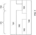
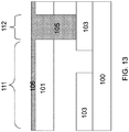
- Defining a first region 111 and a second 112 region in the structural layer 101 may comprise defining a contact region and a suspended region respectively in the structural layer.
- the suspended region defines the region where there is no contact with an underlying layer 103.
- the contact region defines the region of the structural layer 101 where the suspended region is anchored or connected to the underlying layer 103.
- a flexible beam is an example of a structural layer.
- a MEMS beam is typically formed in a structural layer comprising a freestanding part of the beam and an anchor of the beam, where the flexible beam is connected to the underlying layer 103.
- a structural layer for a MEMS device typically comprises at least one area with at least one suspended part and at least one contact area.
- the structural layer of the MEMS device may for example comprise a freestanding beam.
- the freestanding beam is attached at an anchor point to its underlying layer 103.
- the structural layer comprises thus an area with suspended parts (the freestanding beam) and a contact area (the anchor point of the freestanding beam).
- the at least one area with suspended parts has a low strain gradient (strain gradient being defined as the positive difference in the strain between top and bottom of the suspended part divided by its thickness), e.g. a strain gradient below 6.8x10 -6 ⁇ m -1
- the at least one contact area has low electrical resistivity, e.g.
- FIG. 1 shows a schematic overview of a stack of layers comprising a substrate layer 100, an underlying layer 103 on the substrate layer 100, a sacrificial layer 102 on the underlying layer 103 and a structural layer 101 on the sacrificial layer 102. After formation of the structure in the structural layer 101, the sacrificial layer 102 is typically removed, thereby forming a cavity in between a free-standing part of the structural layer 101 and the underlying layer 103.
- the calculation of the strain gradient takes into account the deflection and dimension of the structure and is defined by equation (1): 2 ⁇ deflection lengt h 2 with deflection being the deflection from the tip of the cantilever compared to 0 horizontal and with length being the length of the cantilever.
- FIG. 6 shows the different parts of a structural layer for a MEMS device.
- a substrate layer 601 is used as support layer on which multiple alternating layers of structural and sacrificial material are deposited and patterned to realize micromechanical structures.
- a sacrificial layer 602 is formed on a substrate layer 601. The sacrificial layer 602 is patterned to create openings 606 to the underlying substrate layer 601.
- a structural layer 607 is deposited on the sacrificial layer 602 and patterned into the desired geometry, for example a freestanding beam. The sacrificial material 602 is removed and as such part 605 of the structural layer is released at a suspended region, whereas another part 604 of the structural layer remains connected to the underlying substrate layer 601 at the anchor or contact region.
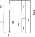
- a shielding layer 104 is provided on the first region 111, as illustrated in FIG. 2 .
- the shielding layer 104 is not present on the second region 112. As long as the shielding layer 104 is present on the first region 111, any thermal treatment performed on the structural layer 101 will only affect the second region 112 and will substantially not affect the first region 111.
- the shielding layer 104 on the first region 111 is shielding the first region 111 during a first annealing step.
- the first region 111 is substantially not influenced by the first annealing step when the shielding layer 104 is present on the first region 111. More specifically the electrical properties and/or mechanical properties of the first region 111 are substantially not influenced by the first annealing step as long as the shielding layer 104 is present on the first region 111.
- the shielding layer 104 may comprise a material which can withstand high thermal fluences, such as e.g. fluences higher than 600mJ/cm 2 , for example 6000 pulses at a laser fluence of 960 mJ/cm 2 , without experiencing any drastic changes or deterioration.
- high thermal fluences such as e.g. fluences higher than 600mJ/cm 2 , for example 6000 pulses at a laser fluence of 960 mJ/cm 2 , without experiencing any drastic changes or deterioration.
- the shielding layer 104 may, alternatively or on top thereof, comprise a reflective material, for example aluminum.
- Aluminum can provide a 90% reflectance.
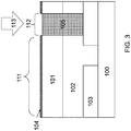
- a first thermal treatment 113 is performed to the structural layer 101. As the first region 111 is protected by the shielding layer 104, only the second region 112 is affected by the first thermal treatment 113 ( FIG. 3 ).
- annealing the second region 112 of the structural layer 101 with a first fluence may comprise thereby converting at least part of the amorphous semiconductor material in the second region 112 into crystalline material.
- the amorphous semiconductor material in the second region 112 may be converted partially or completely.
- the first thermal treatment 113 comprises a first laser annealing step.
- the process parameters of the first annealing step may include a first laser pulse fluence, a first number of laser pulses and a first pulse repetition rate.
- the first annealing step may be characterized by a first fluence which is higher than 600 mJ/cm 2 .
- the first fluence may be between 600-1000 mJ/cm 2 .
- the first number of laser pulses is between 1 and 1000, for example between 1 and 500.
- the number of laser pulses may be selected so as to decrease the crystallization depth to tune the strain gradient.
- the first pulse repetition rate is between 1 Hz and 50 Hz.
- the pulse repetition rate may be selected so as to decrease the crystallization depth to tune the strain gradient.
- the first annealing step comprises one pulse (and not pulse repetition rate) with a fluence between 600-1000 mJ/cm 2 .
- the amorphous semiconductor material of the second region 112 of the structural layer 101 may be converted, partially or completely, into crystalline semiconductor material 105.
- a-SiGe may be converted to poly-SiGe after applying a first annealing step.
- the amorphous semiconductor material of the second region 112 may advantageously be completely converted into crystalline semiconductor material.
- Such complete conversion of the amorphous semiconductor material of the second region 112 is advantageous as the electrical resistivity is lower with larger crystallization depth.
- the crystallization depth in the second region 112 may be equal or smaller than the thickness of the structural layer 101.
- the crystallization depth in the second region 112 may advantageously be equal to the thickness of the structural layer 101, as this results in the lowest resistivity.
- the thermal penetration depth is thus advantageously limited to the amorphous semiconductor layer of the second region 112.
- the initial resistivity of the second region 112 is reduced without substantially affecting the initial resistivity in the first region 111.
- substantially meant that the resistivity of the first region 111 after applying the first annealing step (and before applying a second annealing step) is less than 15 percent lower than the initial resistivity in the first region 111.
- the resistivity of the second region 112 after the first annealing step may be at least 99 percent lower than the initial resistivity thereof.
- the shielding layer 104 is removed ( FIG. 4 ). Removing the shielding layer 104 may be done in any suitable way, for example by a chemical etching step.
- the second thermal treatment 114 may be a second annealing step, more specifically a second laser annealing step.
- the process parameters of the second annealing step may include a second laser pulse fluence, a second number of laser pulses and a second pulse repetition rate.
- the second fluence is smaller than the first fluence.
- the second fluence is advantageously at least 1.5 times smaller, for example at least 2 times smaller, such as for example at least 2.4 times smaller than the first fluence.
- the second fluence may be at least 3 times, for example at least 4 times, such as at least 4.6 times smaller than the first fluence.
- the second fluence may advantageously be smaller than 250mJ/cm 2 , as this ensures a shallow crystallization depth enough to produce flat cantilevers.
- the second number of laser pulses may be between 1 and 1000, or between 1 and 500.
- the first pulse repetition rate may be between 1 Hz and 50 Hz.
- the second laser pulse fluence may be lower than 250 mJ/cm 2 for single pulse and advantageously lower than 130 mJ/cm 2 for multiple pulse.
- the second laser pulse fluence may be between 230-250 mJ/cm 2 for single pulse and may be between 80-130 mJ/cm 2 for multiple pulse, for example for a number of pulses in the range from 100 to 1000 pulses.
- the second number of laser pulses may be between 1 and 1000, or between 1 and 500. If multiple pulses are applied, the second pulse repetition rate may be between 1 Hz and 50 Hz.
- the second laser annealing step may be applied to both the first region 111 and the second region 112.
- the second fluence is lower than the first fluence, for example at least 1.5 times smaller, for example at least 2 times smaller, such as for example at least 2.4 times smaller
- the second region 112 is substantially not influenced by the second fluence.
- the resistivity of the second region 112 is substantially not changed after the second thermal treatment step 114.
- the initial strain gradient is decreased in the first region 111.
- the second annealing step may be applied to only the first region 111. This would require a second shielding step (not illustrated in the drawings).
- the initial strain gradient in the first region 111 may thus be decreased to a predetermined strain gradient.
- the parameters of the second annealing step (such as pulse fluence, pulse rate, number of pulses) may be chosen such that compressive stress from the deposited amorphous semiconductor layer 101 is reduced by the second annealing step. More particularly the initial strain, for example the initial compressive stress of the amorphous semiconductor layer 101, may be converted to a low tensile stress by the second annealing step.
- the first thermal treatment 113 may be a harsh laser annealing step, whereas the second thermal treatment 114 may be a soft laser annealing step.
- both electrical (low resistivity) and mechanical properties (low strain gradient) are optimized for a structural layer for micromachined applications.
- the fact whether electrical properties (resistivity) or mechanical properties (strain gradient) are changed depend on the parameters of the fluencies.
- Laser annealing influences both electrical and mechanical parameters at the same time.
- the first treatment is tuned to optimize electrical properties but if one would check mechanical properties, excessive tensile stress and strain gradient would be found. That is why a shielding layer, such as for example an aluminum shielding layer, may be used to protect suspended structures during the first laser annealing treatment.
- the first laser treatment is applied only on locations where good electrical properties are desired, for example on anchored contacts. It is advantageous that such locations can withstand the excessive stress because they are not suspended.
- the second treatment is tuned to optimize mechanical properties because of its importance in suspended structures. If one would check the electrical properties, a resistivity would be found that is lower than that of amorphous semiconductor material, e.g. a-SiGe, but not as low as that in the second region 112. Laser fluence is proportional to the electrical resistivity.
- annealing 114 the first 111 and the second region 112 of the structural layer 101 with a second fluence comprises annealing thereby converting at least part of the amorphous semiconductor material in the first region 111.
- At least part of the amorphous semiconductor material in the first region 111 may comprise at least the upper part of the amorphous semiconductor material in the first region 111 ( FIG. 5 ).
- the upper part of the first region 111 of the structural layer 101 may be converted into crystalline semiconductor material 106.
- the a-SiGe may be converted into poly-SiGe in the second region 112 during the first thermal treatment and the a-SiGe from an upper part of the first region 111 may be converted into poly-SiGe in the first region 111.
- the crystallization depth in the first region may be about 200 nm or lower.
- the first and the second annealing step may be performed using a pulsed excimer laser.
- the sacrificial layer 102 may be removed as such forming a free standing structural layer with first region 111 not in connection with the underlying layer 103 and an anchor point as such connecting the second region 112 of the structural layer 101 with the underlying layer 103 ( FIG. 13 ).
- Converting the amorphous semiconductor material may comprise converting the amorphous semiconductor material into crystalline semiconductor material.
- the amorphous semiconductor material may for example be amorphous silicon germanium.
- annealing for example by laser annealing, the amorphous silicon germanium (a-SiGe), the amorphous silicon germanium is converted into crystalline silicon germanium (poly-SiGe).
- a-SiGe amorphous silicon germanium
- poly-SiGe crystalline silicon germanium
- at least part of the amorphous semiconductor layer or the complete amorphous semiconductor layer 101 may be converted into crystalline semiconductor material.
- a structural layer for micromachined applications may be formed which is optimized in terms of electrical and/or mechanical properties, e.g. resistivity and/or strain gradient.
- the structural layer 101 may comprise one part 105 with a predetermined strain gradient and another part 106 with a predetermined resistivity.
- the predetermined strain gradient is lower than the initial strain gradient.
- the predetermined resistivity is lower than the initial resistivity.
- a first and a second annealing step may be applied to the second (contact) region and a second annealing step may be applied to the first (suspended) region of the structural layer 101.
- the electrical properties for the second region 112 are optimized, whereas after applying the second annealing step the mechanical properties of the first region 111 are optimized.
- the second region 112 is characterized by a predetermined resistivity being different from the initial resistivity.
- the predetermined resistivity may be smaller than the initial resistivity.
- the first region 111 is characterized by a predetermined strain gradient being different from the initial strain gradient.
- the predetermined strain gradient may be smaller than the initial strain gradient.
- FIG. 9 shows experimental results for PECVD SiGe layers which were prepared at 210°C on Si wafers 905 covered with 2 ⁇ m SiO 2 903.
- a 200 nm a-Si layer 904 was used in between the B-doped Si 72 Ge 28 901 and the 2 ⁇ m thick sacrificial oxide 903 for improved adhesion.
- the SiGe layers were 1.0, 1.6 and 1.8 ⁇ m thick.
- the electrical and mechanical properties of the as grown amorphous and laser annealed layers were determined as follows. The sheet resistance and surface roughness was measured on blanket samples using a four-point probe and Dektak surface profiler, respectively. The strain gradient was determined from the cantilever out of plane deflection.
- Laser crystallization on blanket and patterned samples was performed using a KrF Excimer laser (248 nm) with a 23 mm 2 spot size and a 24 ns pulse duration.
- Blanket samples underwent a harsh laser treatment to increase the crystallization depth and reduce the resistivity of the layers, while the laser fluence was restricted to a maximum of 120 mJ/cm 2 for the strain gradient optimization in patterned samples.
- harsh laser treatment is meant a laser treatment with a fluence higher than 600 mJ/cm 2 up to 1000 mJ/cm 2 )
- Al Aluminum
- LA harsh laser annealing
- Al layers were deposited, by sputtering at room temperature, directly on a-SiGe. They were either patterned or left blanket and exposed to the laser beam. After treatment, surface roughness changes were monitored on the blanket Al layers to examine the layer's endurance to the harsh laser annealing conditions.
- the Al was removed after the laser treatment by a wet etch in diluted HF.
- the underlying SiGe layer was then examined by SEM to detect visible changes between the exposed and unexposed SiGe. Additionally the sheet resistance and surface roughness were measured in both treated and untreated locations and compared to that of the as-grown a-SiGe and previously laser annealed poly-SiGe samples.
- As-grown deposited layers were tuned to be highly compressive.
- the laser pulse shifted the stress to more tensile values, and layers with an initial high compressive stress had a higher limit for the maximum laser fluence.
- a low Ge concentration of 28% turned out to be more efficient in enduring harsh laser annealing conditions. Higher Ge concentrations lowered the material's melting point and therefore were more sensitive to slight variations in the laser pulse.
- FIG. 7 shows a secondary electron microscopy (SEM) image of released cantilevers 701 before the laser annealing treatment.
- Figure 8 shows a secondary electron microscopy (SEM) image of released cantilevers 801 after a laser annealing treatment with 500 pulses at 10 Hz and 120 mJ/cm 2 resulting in a reduced strain gradient.
- Either a single or multiple pulse technique can be used to minimize the strain gradient.
- 500 pulses at 10 Hz and 120 mJ/cm2 are sufficient to reduce the strain gradient to -1.6 ⁇ 10 -7 ⁇ m -1 .
- a treatment at this laser fluence results in a moderate resistivity of 35.8 m ⁇ cm.
- a limitation to ensure reduced strain gradient values is to keep the total supplied energy for a single pulse treatment below 240 mJ/cm 2 . This will affect the maximum crystallization depth.
- FIG. 9 shows a TEM image for a multiple pulse treatment of 500 pulses at 10 Hz and 120 mJ/cm 2 applied to a 1.8 ⁇ m thick Si 72 Ge 28 layer 901. After the laser treatment only upper part of the Si 72 Ge 28 layer 901 is converted into polycrystalline SiGe (poly-SiGe) 902. A crystallization depth of only 0.2 ⁇ m is achieved.
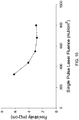
- FIG. 10 outlines the effect of a single pulse fluence on the resistivity of a Si 72 Ge 28 sample.
- the resistivity is plotted in function of the single pulse fluence.
- a laser fluence of 680 mJ/cm 2 is sufficient to reduce the resistivity to a low value of 2.83 ⁇ m ⁇ cm with a surface roughness of 125.5 nm.
- the crystallization depth produced by such a treatment is 1 ⁇ m as seen in FIG. 11.
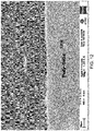
- FIG. 11 shows a TEM image of a poly-SiGe layer 1102 achieved after performing a laser treatment to a 1.6 ⁇ m thick Si 72 Ge 28 layer with a single fluence pulse of 680 mJ/cm 2 .
- a crystallization depth of approximately 0.6-1 ⁇ m is achieved.
- a variation in grain size is visible across the depth of the layer due to a temperature gradient during the laser annealing step.
- a layer of larger grains 1102, about 0.57 ⁇ m deep, is measured, as well as a layer of finer grains 1101, about 0.25 ⁇ m deep.
- the poly-SiGe layer is formed on a 200 nm a-Si layer (not clearly visible in FIG. 11 , but as layer 904 in FIG. 9 ).
- FIG. 11 furthermore shows a CVD oxide layer 1103, which is added during TEM analysis to protect the sample during sample preparation.
- FIG. 12 displays a SEM image of an a-SiGe layer partly shielded and exposed to a high laser fluence.
- the apparent change between the exposed 1202 and unexposed 1201 SiGe surface roughness is clearly visible.
- the surface roughness of the exposed poly-SiGe areas 1202 is increased to 174 nm, similar to the value obtained previously for the 1.8 ⁇ m thick sample treated with the same fluence.
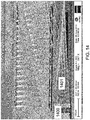
- FIG. 14 shows a secondary electron microscopy (SEM) image of a series of cantilevers manufactured according to embodiments of the present invention.
- the suspended area 1401 was shielded with an aluminum layer when applying a first laser anneal to contact area 1400 of the series of cantilevers.
- a laser energy of 100mJ was applied and it can be seen that the released cantilevers suffer from strain (bending cantilevers).
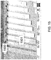
- FIG. 15 shows a secondary electron microscopy (SEM) image of a series of cantilevers manufactured according to embodiments of the present invention.
- the suspended area 1501 was shielded with an aluminum layer when applying a first laser anneal to contact area 1500 of the series of cantilevers. A laser energy of 100mJ was applied. Thereafter the aluminum layer was removed and a second laser anneal was applied to both the contact area 1500 and the suspended area 1501 of the series of cantilevers.
- the first anneal was a single pulse anneal of 100mJ
- the second anneal was a pulsed anneal of 20mJ and 1000 pulses at 20Hz. It can be seen that the released cantilevers do not suffer from strain and are nicely released without any bending.
- Embodiments of the present invention demonstrated the possibility to realize semiconductor films, in particular SiGe films, deposited at 210 °C with a low resistivity in the contact areas (down to 3.47 m ⁇ cm) and a low strain gradient of -1.6 ⁇ 10 -7 ⁇ m -1 for the freestanding structures using a 2-step laser annealing process of which 1 step uses a patterned shielding layer, e.g. a patterned Al shielding layer.
- the A1 shield is highly reflective to the UV radiation and no drastic changes are detected in the shield after laser anneal.
Landscapes
- Engineering & Computer Science (AREA)
- Manufacturing & Machinery (AREA)
- Microelectronics & Electronic Packaging (AREA)
- Mechanical Engineering (AREA)
- Micromachines (AREA)
- Thin Film Transistor (AREA)
Applications Claiming Priority (1)
| Application Number | Priority Date | Filing Date | Title |
|---|---|---|---|
| US29739210P | 2010-01-22 | 2010-01-22 |
Publications (3)
| Publication Number | Publication Date |
|---|---|
| EP2347993A2 EP2347993A2 (en) | 2011-07-27 |
| EP2347993A3 EP2347993A3 (en) | 2012-03-07 |
| EP2347993B1 true EP2347993B1 (en) | 2018-11-14 |
Family
ID=43807129
Family Applications (1)
| Application Number | Title | Priority Date | Filing Date |
|---|---|---|---|
| EP11151337.0A Not-in-force EP2347993B1 (en) | 2010-01-22 | 2011-01-19 | Method for manufacturing a micromachined device and micromachined device made thereof |
Country Status (3)
| Country | Link |
|---|---|
| US (1) | US8383441B2 (enExample) |
| EP (1) | EP2347993B1 (enExample) |
| JP (1) | JP5529053B2 (enExample) |
Families Citing this family (5)
| Publication number | Priority date | Publication date | Assignee | Title |
|---|---|---|---|---|
| WO2014003843A1 (en) * | 2012-06-29 | 2014-01-03 | Regents Of The University Of Minnesota | Method of forming individual metallic microstructures |
| US9039753B2 (en) | 2012-09-05 | 2015-05-26 | Jeff Thramann | System and method to electrically charge implantable devices |
| US9484199B2 (en) | 2013-09-06 | 2016-11-01 | Applied Materials, Inc. | PECVD microcrystalline silicon germanium (SiGe) |
| JP2019054143A (ja) * | 2017-09-15 | 2019-04-04 | 株式会社東芝 | 接続構造およびその製造方法ならびにセンサ |
| EP3916122A1 (en) | 2020-05-28 | 2021-12-01 | Solmates B.V. | Method for controlling stress in a substrate during laser deposition |
Family Cites Families (11)
| Publication number | Priority date | Publication date | Assignee | Title |
|---|---|---|---|---|
| JPS6054277B2 (ja) | 1981-08-08 | 1985-11-29 | 富士通株式会社 | 非単結晶半導体層の単結晶化方法 |
| US4475955A (en) * | 1982-12-06 | 1984-10-09 | Harris Corporation | Method for forming integrated circuits bearing polysilicon of reduced resistance |
| US20020192914A1 (en) * | 2001-06-15 | 2002-12-19 | Kizilyalli Isik C. | CMOS device fabrication utilizing selective laser anneal to form raised source/drain areas |
| US7763947B2 (en) * | 2002-04-23 | 2010-07-27 | Sharp Laboratories Of America, Inc. | Piezo-diode cantilever MEMS |
| US6922272B1 (en) * | 2003-02-14 | 2005-07-26 | Silicon Light Machines Corporation | Method and apparatus for leveling thermal stress variations in multi-layer MEMS devices |
| KR100954332B1 (ko) * | 2003-06-30 | 2010-04-21 | 엘지디스플레이 주식회사 | 액정표시소자와 그 제조방법 |
| US20050048706A1 (en) * | 2003-08-27 | 2005-03-03 | Semiconductor Energy Laboratory Co., Ltd. | Method of manufacturing semiconductor device |
| US7696031B2 (en) * | 2004-06-14 | 2010-04-13 | Semiconductor Energy Laboratory Co., Ltd | Method for manufacturing semiconductor device |
| EP1801067A3 (en) | 2005-12-21 | 2012-05-09 | Imec | Method for forming silicon germanium layers at low temperatures for controlling stress gradient |
| US7651896B2 (en) * | 2006-08-30 | 2010-01-26 | Semiconductor Energy Laboratory Co., Ltd. | Method for manufacturing semiconductor device |
| US20110068342A1 (en) * | 2009-09-18 | 2011-03-24 | Themistokles Afentakis | Laser Process for Minimizing Variations in Transistor Threshold Voltages |
-
2011
- 2011-01-19 EP EP11151337.0A patent/EP2347993B1/en not_active Not-in-force
- 2011-01-21 US US13/010,923 patent/US8383441B2/en not_active Expired - Fee Related
- 2011-01-21 JP JP2011011011A patent/JP5529053B2/ja not_active Expired - Fee Related
Non-Patent Citations (1)
| Title |
|---|
| None * |
Also Published As
| Publication number | Publication date |
|---|---|
| JP2011148087A (ja) | 2011-08-04 |
| EP2347993A3 (en) | 2012-03-07 |
| JP5529053B2 (ja) | 2014-06-25 |
| US20110180886A1 (en) | 2011-07-28 |
| US8383441B2 (en) | 2013-02-26 |
| EP2347993A2 (en) | 2011-07-27 |
Similar Documents
| Publication | Publication Date | Title |
|---|---|---|
| US8367451B2 (en) | Method and structures for fabricating MEMS devices on compliant layers | |
| EP2347993B1 (en) | Method for manufacturing a micromachined device and micromachined device made thereof | |
| Smith et al. | Excimer laser crystallization and doping of silicon films on plastic substrates | |
| EP0841167B1 (en) | Method of producing a through-hole and the use of said method to produce a silicon substrate having a through-hole or a device using such a substrate, method of producing an ink jet print head and use of said method for producing an ink jet print head | |
| US8466042B2 (en) | Method for manufacturing separated micromechanical components situated on a silicon substrate and components manufactured therefrom | |
| US20090142872A1 (en) | Fabrication of capacitive micromachined ultrasonic transducers by local oxidation | |
| EP2075826A3 (fr) | Procédé de fabrication d'un substrat semiconducteur-sur-isolant comprenant une étape d'enrichissement en Ge localisé | |
| JP4686544B2 (ja) | 基板上で層をエッチングする方法 | |
| Wang et al. | Avoiding blister defects in low-stress hydrogenated amorphous silicon films for MEMS sensors | |
| EP1801067A2 (en) | Method for forming silicon germanium layers at low temperatures for controlling stress gradient | |
| DE102011006332A1 (de) | Verfahren zum Erzeugen von monokristallinen Piezowiderständen | |
| CN1872657B (zh) | 微结构及其制造方法 | |
| US8709957B2 (en) | Spalling utilizing stressor layer portions | |
| US8093088B2 (en) | Manufacturing method of micro-electro-mechanical device | |
| US8247319B1 (en) | Method to enable the process and enlarge the process window for silicide, germanide or germanosilicide formation in structures with extremely small dimensions | |
| US20130316538A1 (en) | Surface morphology generation and transfer by spalling | |
| TW200906708A (en) | Polysilicon deposition and anneal process enabling thick polysilicon films for MEMS applications | |
| Monk et al. | Stress-corrosion cracking and blistering of thin polycrystalline silicon films in hydrofluoric acid | |
| El-Rifai et al. | Selective laser annealing for improved SiGe MEMS structural layers at 210° C | |
| EP2099064A1 (en) | Method for manufacturing a semiconductor device | |
| WO2011019282A1 (en) | Method for manufacturing a single crystal nano-wire. | |
| EP1627422B1 (fr) | Procede de delimitation d'un element conducteur dispose sur une couche isolante | |
| US7470462B2 (en) | Method to control residual stress in a film structure and a system thereof | |
| Kline et al. | Suppression of Dewetting in Pulsed Laser Melting of Thin Metallic Films on SiO2 | |
| US8853797B2 (en) | MEMS devices and fabrication thereof |
Legal Events
| Date | Code | Title | Description |
|---|---|---|---|
| PUAI | Public reference made under article 153(3) epc to a published international application that has entered the european phase |
Free format text: ORIGINAL CODE: 0009012 |
|
| AK | Designated contracting states |
Kind code of ref document: A2 Designated state(s): AL AT BE BG CH CY CZ DE DK EE ES FI FR GB GR HR HU IE IS IT LI LT LU LV MC MK MT NL NO PL PT RO RS SE SI SK SM TR |
|
| AX | Request for extension of the european patent |
Extension state: BA ME |
|
| PUAL | Search report despatched |
Free format text: ORIGINAL CODE: 0009013 |
|
| AK | Designated contracting states |
Kind code of ref document: A3 Designated state(s): AL AT BE BG CH CY CZ DE DK EE ES FI FR GB GR HR HU IE IS IT LI LT LU LV MC MK MT NL NO PL PT RO RS SE SI SK SM TR |
|
| AX | Request for extension of the european patent |
Extension state: BA ME |
|
| RIC1 | Information provided on ipc code assigned before grant |
Ipc: B81C 1/00 20060101AFI20120203BHEP |
|
| 17P | Request for examination filed |
Effective date: 20120906 |
|
| RAP1 | Party data changed (applicant data changed or rights of an application transferred) |
Owner name: AMERICAN UNIVERSITY CAIRO Owner name: KATHOLIEKE UNIVERSITEIT LEUVEN, K.U. LEUVEN R&D Owner name: IMEC VZW |
|
| GRAP | Despatch of communication of intention to grant a patent |
Free format text: ORIGINAL CODE: EPIDOSNIGR1 |
|
| RIN1 | Information on inventor provided before grant (corrected) |
Inventor name: ABDEL AZIZ, AHMED KAMAL SAID Inventor name: SEDKY, SHERIF Inventor name: EL RIFAI, JOUMANA Inventor name: WITVROUW, ANN |
|
| STAA | Information on the status of an ep patent application or granted ep patent |
Free format text: STATUS: GRANT OF PATENT IS INTENDED |
|
| INTG | Intention to grant announced |
Effective date: 20180329 |
|
| RIN1 | Information on inventor provided before grant (corrected) |
Inventor name: SEDKY, SHERIF Inventor name: ABDEL AZIZ, AHMED KAMAL SAID Inventor name: EL RIFAI, JOUMANA Inventor name: WITVROUW, ANN |
|
| GRAS | Grant fee paid |
Free format text: ORIGINAL CODE: EPIDOSNIGR3 |
|
| GRAJ | Information related to disapproval of communication of intention to grant by the applicant or resumption of examination proceedings by the epo deleted |
Free format text: ORIGINAL CODE: EPIDOSDIGR1 |
|
| GRAL | Information related to payment of fee for publishing/printing deleted |
Free format text: ORIGINAL CODE: EPIDOSDIGR3 |
|
| STAA | Information on the status of an ep patent application or granted ep patent |
Free format text: STATUS: REQUEST FOR EXAMINATION WAS MADE |
|
| INTC | Intention to grant announced (deleted) | ||
| GRAR | Information related to intention to grant a patent recorded |
Free format text: ORIGINAL CODE: EPIDOSNIGR71 |
|
| STAA | Information on the status of an ep patent application or granted ep patent |
Free format text: STATUS: GRANT OF PATENT IS INTENDED |
|
| GRAA | (expected) grant |
Free format text: ORIGINAL CODE: 0009210 |
|
| STAA | Information on the status of an ep patent application or granted ep patent |
Free format text: STATUS: THE PATENT HAS BEEN GRANTED |
|
| INTG | Intention to grant announced |
Effective date: 20181004 |
|
| AK | Designated contracting states |
Kind code of ref document: B1 Designated state(s): AL AT BE BG CH CY CZ DE DK EE ES FI FR GB GR HR HU IE IS IT LI LT LU LV MC MK MT NL NO PL PT RO RS SE SI SK SM TR |
|
| REG | Reference to a national code |
Ref country code: GB Ref legal event code: FG4D |
|
| REG | Reference to a national code |
Ref country code: CH Ref legal event code: EP Ref country code: AT Ref legal event code: REF Ref document number: 1064546 Country of ref document: AT Kind code of ref document: T Effective date: 20181115 |
|
| REG | Reference to a national code |
Ref country code: DE Ref legal event code: R096 Ref document number: 602011053790 Country of ref document: DE |
|
| REG | Reference to a national code |
Ref country code: IE Ref legal event code: FG4D |
|
| REG | Reference to a national code |
Ref country code: NL Ref legal event code: MP Effective date: 20181114 |
|
| REG | Reference to a national code |
Ref country code: LT Ref legal event code: MG4D |
|
| REG | Reference to a national code |
Ref country code: AT Ref legal event code: MK05 Ref document number: 1064546 Country of ref document: AT Kind code of ref document: T Effective date: 20181114 |
|
| PG25 | Lapsed in a contracting state [announced via postgrant information from national office to epo] |
Ref country code: LV Free format text: LAPSE BECAUSE OF FAILURE TO SUBMIT A TRANSLATION OF THE DESCRIPTION OR TO PAY THE FEE WITHIN THE PRESCRIBED TIME-LIMIT Effective date: 20181114 Ref country code: HR Free format text: LAPSE BECAUSE OF FAILURE TO SUBMIT A TRANSLATION OF THE DESCRIPTION OR TO PAY THE FEE WITHIN THE PRESCRIBED TIME-LIMIT Effective date: 20181114 Ref country code: AT Free format text: LAPSE BECAUSE OF FAILURE TO SUBMIT A TRANSLATION OF THE DESCRIPTION OR TO PAY THE FEE WITHIN THE PRESCRIBED TIME-LIMIT Effective date: 20181114 Ref country code: FI Free format text: LAPSE BECAUSE OF FAILURE TO SUBMIT A TRANSLATION OF THE DESCRIPTION OR TO PAY THE FEE WITHIN THE PRESCRIBED TIME-LIMIT Effective date: 20181114 Ref country code: ES Free format text: LAPSE BECAUSE OF FAILURE TO SUBMIT A TRANSLATION OF THE DESCRIPTION OR TO PAY THE FEE WITHIN THE PRESCRIBED TIME-LIMIT Effective date: 20181114 Ref country code: BG Free format text: LAPSE BECAUSE OF FAILURE TO SUBMIT A TRANSLATION OF THE DESCRIPTION OR TO PAY THE FEE WITHIN THE PRESCRIBED TIME-LIMIT Effective date: 20190214 Ref country code: NO Free format text: LAPSE BECAUSE OF FAILURE TO SUBMIT A TRANSLATION OF THE DESCRIPTION OR TO PAY THE FEE WITHIN THE PRESCRIBED TIME-LIMIT Effective date: 20190214 Ref country code: LT Free format text: LAPSE BECAUSE OF FAILURE TO SUBMIT A TRANSLATION OF THE DESCRIPTION OR TO PAY THE FEE WITHIN THE PRESCRIBED TIME-LIMIT Effective date: 20181114 Ref country code: IS Free format text: LAPSE BECAUSE OF FAILURE TO SUBMIT A TRANSLATION OF THE DESCRIPTION OR TO PAY THE FEE WITHIN THE PRESCRIBED TIME-LIMIT Effective date: 20190314 |
|
| PG25 | Lapsed in a contracting state [announced via postgrant information from national office to epo] |
Ref country code: GR Free format text: LAPSE BECAUSE OF FAILURE TO SUBMIT A TRANSLATION OF THE DESCRIPTION OR TO PAY THE FEE WITHIN THE PRESCRIBED TIME-LIMIT Effective date: 20190215 Ref country code: PT Free format text: LAPSE BECAUSE OF FAILURE TO SUBMIT A TRANSLATION OF THE DESCRIPTION OR TO PAY THE FEE WITHIN THE PRESCRIBED TIME-LIMIT Effective date: 20190314 Ref country code: NL Free format text: LAPSE BECAUSE OF FAILURE TO SUBMIT A TRANSLATION OF THE DESCRIPTION OR TO PAY THE FEE WITHIN THE PRESCRIBED TIME-LIMIT Effective date: 20181114 Ref country code: AL Free format text: LAPSE BECAUSE OF FAILURE TO SUBMIT A TRANSLATION OF THE DESCRIPTION OR TO PAY THE FEE WITHIN THE PRESCRIBED TIME-LIMIT Effective date: 20181114 Ref country code: RS Free format text: LAPSE BECAUSE OF FAILURE TO SUBMIT A TRANSLATION OF THE DESCRIPTION OR TO PAY THE FEE WITHIN THE PRESCRIBED TIME-LIMIT Effective date: 20181114 Ref country code: SE Free format text: LAPSE BECAUSE OF FAILURE TO SUBMIT A TRANSLATION OF THE DESCRIPTION OR TO PAY THE FEE WITHIN THE PRESCRIBED TIME-LIMIT Effective date: 20181114 |
|
| PG25 | Lapsed in a contracting state [announced via postgrant information from national office to epo] |
Ref country code: DK Free format text: LAPSE BECAUSE OF FAILURE TO SUBMIT A TRANSLATION OF THE DESCRIPTION OR TO PAY THE FEE WITHIN THE PRESCRIBED TIME-LIMIT Effective date: 20181114 Ref country code: PL Free format text: LAPSE BECAUSE OF FAILURE TO SUBMIT A TRANSLATION OF THE DESCRIPTION OR TO PAY THE FEE WITHIN THE PRESCRIBED TIME-LIMIT Effective date: 20181114 Ref country code: CZ Free format text: LAPSE BECAUSE OF FAILURE TO SUBMIT A TRANSLATION OF THE DESCRIPTION OR TO PAY THE FEE WITHIN THE PRESCRIBED TIME-LIMIT Effective date: 20181114 Ref country code: IT Free format text: LAPSE BECAUSE OF FAILURE TO SUBMIT A TRANSLATION OF THE DESCRIPTION OR TO PAY THE FEE WITHIN THE PRESCRIBED TIME-LIMIT Effective date: 20181114 |
|
| REG | Reference to a national code |
Ref country code: DE Ref legal event code: R097 Ref document number: 602011053790 Country of ref document: DE |
|
| PG25 | Lapsed in a contracting state [announced via postgrant information from national office to epo] |
Ref country code: MC Free format text: LAPSE BECAUSE OF FAILURE TO SUBMIT A TRANSLATION OF THE DESCRIPTION OR TO PAY THE FEE WITHIN THE PRESCRIBED TIME-LIMIT Effective date: 20181114 Ref country code: SK Free format text: LAPSE BECAUSE OF FAILURE TO SUBMIT A TRANSLATION OF THE DESCRIPTION OR TO PAY THE FEE WITHIN THE PRESCRIBED TIME-LIMIT Effective date: 20181114 Ref country code: EE Free format text: LAPSE BECAUSE OF FAILURE TO SUBMIT A TRANSLATION OF THE DESCRIPTION OR TO PAY THE FEE WITHIN THE PRESCRIBED TIME-LIMIT Effective date: 20181114 Ref country code: SM Free format text: LAPSE BECAUSE OF FAILURE TO SUBMIT A TRANSLATION OF THE DESCRIPTION OR TO PAY THE FEE WITHIN THE PRESCRIBED TIME-LIMIT Effective date: 20181114 Ref country code: RO Free format text: LAPSE BECAUSE OF FAILURE TO SUBMIT A TRANSLATION OF THE DESCRIPTION OR TO PAY THE FEE WITHIN THE PRESCRIBED TIME-LIMIT Effective date: 20181114 |
|
| REG | Reference to a national code |
Ref country code: CH Ref legal event code: PL |
|
| PLBE | No opposition filed within time limit |
Free format text: ORIGINAL CODE: 0009261 |
|
| STAA | Information on the status of an ep patent application or granted ep patent |
Free format text: STATUS: NO OPPOSITION FILED WITHIN TIME LIMIT |
|
| PG25 | Lapsed in a contracting state [announced via postgrant information from national office to epo] |
Ref country code: LU Free format text: LAPSE BECAUSE OF NON-PAYMENT OF DUE FEES Effective date: 20190119 |
|
| REG | Reference to a national code |
Ref country code: BE Ref legal event code: MM Effective date: 20190131 |
|
| 26N | No opposition filed |
Effective date: 20190815 |
|
| GBPC | Gb: european patent ceased through non-payment of renewal fee |
Effective date: 20190214 |
|
| REG | Reference to a national code |
Ref country code: IE Ref legal event code: MM4A |
|
| PG25 | Lapsed in a contracting state [announced via postgrant information from national office to epo] |
Ref country code: SI Free format text: LAPSE BECAUSE OF FAILURE TO SUBMIT A TRANSLATION OF THE DESCRIPTION OR TO PAY THE FEE WITHIN THE PRESCRIBED TIME-LIMIT Effective date: 20181114 |
|
| PG25 | Lapsed in a contracting state [announced via postgrant information from national office to epo] |
Ref country code: BE Free format text: LAPSE BECAUSE OF NON-PAYMENT OF DUE FEES Effective date: 20190131 |
|
| PG25 | Lapsed in a contracting state [announced via postgrant information from national office to epo] |
Ref country code: LI Free format text: LAPSE BECAUSE OF NON-PAYMENT OF DUE FEES Effective date: 20190131 Ref country code: CH Free format text: LAPSE BECAUSE OF NON-PAYMENT OF DUE FEES Effective date: 20190131 |
|
| PG25 | Lapsed in a contracting state [announced via postgrant information from national office to epo] |
Ref country code: GB Free format text: LAPSE BECAUSE OF NON-PAYMENT OF DUE FEES Effective date: 20190214 Ref country code: IE Free format text: LAPSE BECAUSE OF NON-PAYMENT OF DUE FEES Effective date: 20190119 |
|
| PG25 | Lapsed in a contracting state [announced via postgrant information from national office to epo] |
Ref country code: TR Free format text: LAPSE BECAUSE OF FAILURE TO SUBMIT A TRANSLATION OF THE DESCRIPTION OR TO PAY THE FEE WITHIN THE PRESCRIBED TIME-LIMIT Effective date: 20181114 |
|
| PG25 | Lapsed in a contracting state [announced via postgrant information from national office to epo] |
Ref country code: MT Free format text: LAPSE BECAUSE OF NON-PAYMENT OF DUE FEES Effective date: 20190119 |
|
| PGFP | Annual fee paid to national office [announced via postgrant information from national office to epo] |
Ref country code: FR Payment date: 20201217 Year of fee payment: 11 |
|
| PG25 | Lapsed in a contracting state [announced via postgrant information from national office to epo] |
Ref country code: CY Free format text: LAPSE BECAUSE OF FAILURE TO SUBMIT A TRANSLATION OF THE DESCRIPTION OR TO PAY THE FEE WITHIN THE PRESCRIBED TIME-LIMIT Effective date: 20181114 |
|
| PGFP | Annual fee paid to national office [announced via postgrant information from national office to epo] |
Ref country code: DE Payment date: 20201217 Year of fee payment: 11 |
|
| PG25 | Lapsed in a contracting state [announced via postgrant information from national office to epo] |
Ref country code: HU Free format text: LAPSE BECAUSE OF FAILURE TO SUBMIT A TRANSLATION OF THE DESCRIPTION OR TO PAY THE FEE WITHIN THE PRESCRIBED TIME-LIMIT; INVALID AB INITIO Effective date: 20110119 |
|
| PG25 | Lapsed in a contracting state [announced via postgrant information from national office to epo] |
Ref country code: MK Free format text: LAPSE BECAUSE OF FAILURE TO SUBMIT A TRANSLATION OF THE DESCRIPTION OR TO PAY THE FEE WITHIN THE PRESCRIBED TIME-LIMIT Effective date: 20181114 |
|
| REG | Reference to a national code |
Ref country code: DE Ref legal event code: R119 Ref document number: 602011053790 Country of ref document: DE |
|
| PG25 | Lapsed in a contracting state [announced via postgrant information from national office to epo] |
Ref country code: DE Free format text: LAPSE BECAUSE OF NON-PAYMENT OF DUE FEES Effective date: 20220802 |
|
| PG25 | Lapsed in a contracting state [announced via postgrant information from national office to epo] |
Ref country code: FR Free format text: LAPSE BECAUSE OF NON-PAYMENT OF DUE FEES Effective date: 20220131 |