EP2346072A1 - Substrate detection device and method - Google Patents
Substrate detection device and method Download PDFInfo
- Publication number
- EP2346072A1 EP2346072A1 EP09817767A EP09817767A EP2346072A1 EP 2346072 A1 EP2346072 A1 EP 2346072A1 EP 09817767 A EP09817767 A EP 09817767A EP 09817767 A EP09817767 A EP 09817767A EP 2346072 A1 EP2346072 A1 EP 2346072A1
- Authority
- EP
- European Patent Office
- Prior art keywords
- substrates
- light
- collimating reflector
- image
- light source
- Prior art date
- Legal status (The legal status is an assumption and is not a legal conclusion. Google has not performed a legal analysis and makes no representation as to the accuracy of the status listed.)
- Granted
Links
Images


Classifications
-
- H—ELECTRICITY
- H10—SEMICONDUCTOR DEVICES; ELECTRIC SOLID-STATE DEVICES NOT OTHERWISE PROVIDED FOR
- H10P—GENERIC PROCESSES OR APPARATUS FOR THE MANUFACTURE OR TREATMENT OF DEVICES COVERED BY CLASS H10
- H10P72/00—Handling or holding of wafers, substrates or devices during manufacture or treatment thereof
-
- H—ELECTRICITY
- H10—SEMICONDUCTOR DEVICES; ELECTRIC SOLID-STATE DEVICES NOT OTHERWISE PROVIDED FOR
- H10P—GENERIC PROCESSES OR APPARATUS FOR THE MANUFACTURE OR TREATMENT OF DEVICES COVERED BY CLASS H10
- H10P72/00—Handling or holding of wafers, substrates or devices during manufacture or treatment thereof
- H10P72/06—Apparatus for monitoring, sorting, marking, testing or measuring
- H10P72/0606—Position monitoring, e.g. misposition detection or presence detection
- H10P72/0608—Position monitoring, e.g. misposition detection or presence detection of substrates stored in a container, a magazine, a carrier, a boat or the like
-
- H—ELECTRICITY
- H10—SEMICONDUCTOR DEVICES; ELECTRIC SOLID-STATE DEVICES NOT OTHERWISE PROVIDED FOR
- H10P—GENERIC PROCESSES OR APPARATUS FOR THE MANUFACTURE OR TREATMENT OF DEVICES COVERED BY CLASS H10
- H10P72/00—Handling or holding of wafers, substrates or devices during manufacture or treatment thereof
- H10P72/50—Handling or holding of wafers, substrates or devices during manufacture or treatment thereof for positioning, orientation or alignment
-
- Y—GENERAL TAGGING OF NEW TECHNOLOGICAL DEVELOPMENTS; GENERAL TAGGING OF CROSS-SECTIONAL TECHNOLOGIES SPANNING OVER SEVERAL SECTIONS OF THE IPC; TECHNICAL SUBJECTS COVERED BY FORMER USPC CROSS-REFERENCE ART COLLECTIONS [XRACs] AND DIGESTS
- Y10—TECHNICAL SUBJECTS COVERED BY FORMER USPC
- Y10S—TECHNICAL SUBJECTS COVERED BY FORMER USPC CROSS-REFERENCE ART COLLECTIONS [XRACs] AND DIGESTS
- Y10S414/00—Material or article handling
- Y10S414/135—Associated with semiconductor wafer handling
- Y10S414/137—Associated with semiconductor wafer handling including means for charging or discharging wafer cassette
- Y10S414/138—Wafers positioned vertically within cassette
Definitions
- the present invention relates to an apparatus and a method for detecting conditions of a plurality of substrates stored in a cassette.
- this invention is suitable for detecting conditions of a plurality of semiconductor wafers stored in a wafer cassette (or FOUP).
- a method of mapping based on shade detection i.e., a shade sensor scanning method
- this method is intended for mechanically scanning each edge portion of the wafers by using a transmission light switch.
- detecting (unwanted) projections is detecting the conditions of some wafers that are stored in the wafer cassette while projecting forward relative to a preset position.
- the reflectance should be lowered if each wafer is coated with a certain coating agent or the like. Therefore, in some cases, the reflected image cannot be adequately detected, thus relatively degrading the reliability, as compared with the wafer detection method utilizing the transmission light switch.
- the present invention was made in light of the above problems of the related art. Therefore, it is an object of this invention to provide a new substrate detection apparatus and a method of using this apparatus, which can detect more accurately and rapidly the conditions of the plurality of substrates stored in the cassette.
- One feature of the present invention is a substrate detection apparatus adapted for detecting conditions of a plurality of substrates stored in a cassette, comprising: a collimating reflector located on one side of the plurality of substrates; illumination means configured to radiate light in a planar state toward the collimating reflector such that edge portions of the substrates are located in an optical path of the light; image acquiring means configured to acquire a passing light image including the edge portions of the substrates, the passing light image being formed on the collimating reflector with the light radiated in the planar state from the illumination means; and image processing means configured to process the passing light image obtained by the image acquiring means, thereby detecting the conditions of the substrates stored in the cassette.
- the illumination means includes a surface light source.
- the illumination means includes a point light source configured to radiate the light toward the collimating reflector, and a retroreflector configured to reflect the light, which has been reflected and collimated by the collimating reflector, toward the collimating reflector.
- the point light source and image acquiring means are arranged substantially coaxially relative to each other.
- the surface light source or point light source includes a light emitting diode.
- the collimating reflector includes a parabolic mirror.
- the collimating reflector includes a curved mirror formed of a plurality of flat mirrors combined together into a substantially curved surface as a whole.
- Another feature of the present invention is a method of detecting the conditions of the plurality of substrates stored in the cassette, comprising: an illumination step of radiating light in a planar state from an illumination means toward a collimating reflector located on one side of the substrates such that edge portions of the substrates are located in an optical path of the light; an image acquiring step of taking a passing light image including the edge portions of the substrates by using an image acquiring means, the passing light image being formed on the collimating reflector with the light radiated in the planar state from the illumination means; and a detection step of processing the passing light image obtained by the image acquiring means by using an image processing means, thereby detecting the conditions of the substrates.
- the illumination means includes the surface light source.
- the light is radiated toward the collimating reflector from a point light source, and the light, which has been reflected and collimated by the collimating reflector, is then reflected toward the collimating reflector by a retroreflector with the edge portions of substrates located in the optical path of the light.
- the point light source and image acquiring means are arranged substantially coaxially relative to each other.
- the surface light source or point light source includes the light emitting diode.
- the collimating reflector includes the parabolic mirror.
- the collimating reflector includes the curved mirror formed of the plurality of flat mirrors combined together into the substantially curved surface as a whole.
- the substrate detection apparatus 1 is configured for detecting conditions of a plurality of semiconductor wafers 11 respectively stored in a FOUP (or wafer cassette) 10.
- Each semiconductor wafer 11 has a flat disk-like shape and is carried in and carried out relative to the FOUP 10 by a hand attached to a distal arm end of a wafer carrier robot.
- a bright point light source 2 including a light emitting diode (LED) is provided in a substantially coaxial position relative to an image acquiring means 3 including a CCD camera (or single-lens camera).
- the light emitted from the point light source 2 is radiated toward a collimating reflector 4 including a radiation mirror, and is then collimated by the collimating reflector 4.
- the collimating reflector 4 may include a curved mirror formed of a plurality of small flat mirrors combined together into a substantially curved surface as a whole.
- a retroreflector 5 is arranged to be opposed to the collimating reflector 4.
- This retroreflector 5 includes a ⁇ -CCR plate (CCR: Corner Cube Reflector).
- the image acquiring means 3 is connected with an image processing means 6 via a transmission cable. Namely, each image obtained by the image acquiring means 3 will be transmitted to the image processing means 6 via the transmission cable.
- the light is first radiated from the point light source 2, and is then reflected and collimated by the collimating reflector 4.
- the light reflected by the collimating reflector 4 is reflected again, toward the collimating reflector 4, by the retroreflector 5 arranged to be opposed to the collimating reflector 4 (Illumination step).
- a passing light image including each edge portion of the plurality of wafers 11 is formed on the collimating reflector 4 with the light reflected by the retroreflector 4. Namely, in an optical path of the reflected light reflected toward the collimating reflector 4 by the retroreflector 5, the edge portions of the plurality of wafers 11 are located, respectively.
- the passing light image that is formed on the collimating reflector 4 and includes the respective edge portions of the plurality of wafers 11 is acquired by the image acquiring means 3 which includes the CCD camera (Image acquiring step).
- a mirror normal line with respect to the collimating reflector 4 is arranged, in a plan view, to be parallel with a camera optical axis of the image acquiring means (or CCD camera) 3.
- each image of the wafers can be formed to be parallel, relative to one another, in the passing light image.
- Fig. 2 schematically shows the passing light image 20 formed on the collimating reflector 4 and obtained by the image acquiring means 3.
- judgment on whether or not the wafer 11 is present in each slot of the cassette 10 judgment on presence of any double wafer, judgment on presence of any crossing wafer, and/or judgment on presence of any projecting wafer (or amount of projection thereof) can be performed.
- double wafer refers to the case in which two wafers are stored in the same slot while being overlapped relative to each other.
- crossing wafer refers to the case in which the wafer is stored between left and right slots of different levels.
- projecting wafer refers to the case in which the wafer is stored in the wafer cassette while projecting forward relative to a preset position.
- the shade portion corresponding to this case is lacked.
- the shade portion corresponding to this case has a greater length in a Y-axial direction, as compared with the other shade portions.
- the shade portion corresponding to this case has a greater width in an X-axial direction, as compared with the other shade portions. Besides, this shade portion is seen over two slots of different levels. Additionally or alternatively, if the double wafer is present, the shade portion corresponding to this case is double the width in the X-axial direction, as compared with the other shade portions.
- this embodiment employs one kind of the image processing method utilizing the camera.
- this method is somewhat close to a scanning method using a transmission shade sensor. Therefore, this image processing method is less susceptible to the reflectance of each wafer 11 to be detected, thus providing more reliable detection on the conditions of each wafer 11 stored in the cassette.
- the senor can serve to securely detect the projection of some wafers 11, while serving as the mapping sensor. This effect cannot be obtained by performing the scanning operation only once with the transmission shade sensor of the related art.
- each wafer 11 projecting out from the preset position can be detected from a change in the length in the Y-axial direction of each corresponding shade portion, the amount of projection of the wafer 11 can be readily quantified.
- This embodiment can eliminate necessity for the mechanical scanning operation as performed with the conventional transmission shade sensor, thus significantly simplifying the entire system as well as reducing the time required for the detection.
- the detection on the double wafer can be judged from a value of the area of each shade portion, wherein each detected value is markedly changed between the case of the double wafer and the normal case. Therefore, as compared with the related art utilizing each profile of an object, the detection on the double wafer can be performed more securely.
- the passing light image 20 for all of the wafers 11 can be obtained at a time by using the single camera, a significantly small and compact substrate detection apparatus 1 can be achieved.
- the light emitted from the point light source 2 is first reflected and collimated by the collimating reflector 4. Then, the collimated light is further reflected by the retroreflector 5.
- a transmission surface light source 12 is provided in place of the retroreflector 5 shown in Figs. 1A and 1B , such that the collimated light can be radiated from the surface light source 12 toward the collimating reflector 4.
- the transmission surface light source 12 includes an LED light source 13 having LED elements longitudinally arranged in a line therein, and a diffusion transmission plate 14 configured to transmit therethrough the light radiated from the LED light source 13.
- the diffusion transmission plate 14 includes an obscure or frosted glass plate.
- the light just after radiated from the LED light source 13 is in a relatively uneven state.
- this light can be changed into a surface light source having a substantially even and homogeneous brightness.
- the same effect as obtained by the substrate detection apparatus 1 shown in Figs. 1A and 1B can be obtained.
- the passing light image that is formed on the collimating reflector 4 and includes the respective edge portions of the plurality of wafers 11 can be similarly acquired by using the image acquiring means 3 including the CCD camera. Then, the so-obtained passing light image can be analyzed in the same manner by using the image processing means 6.
- Fig. 4 shows another substrate detection apparatus 1B according to one modification of the embodiment shown in Fig. 3 .
- a reflection surface light source 15 is used.
- this reflection surface light source 15 the light is first radiated from the LED light source 13 and then reflected by a diffusion reflector 16.
- the light can also be radiated toward the collimating reflector 4, while being in an adequately even and homogeneous state.
- the substrates 11 are transferred by a substrate carrier robot (hereinafter simply called “robot") from one cassette to the other cassette after the conditions of containing the substrates 11 in the cassette 10 are detected.
- robot substrate carrier robot
- the substrate detection apparatus when the conditions of containing the substrates 11 are detected by the substrate detection apparatus according to the present invention, even if a substrate 11 is dislocated from a preset position, it can be judged whether the substrate 11 can be transferred by correcting some operational parameters, such as operational positions, of the robot. Accordingly, when a transfer of the substrate 11 has been judged to be doable, the substrate 11 can be transferred by correcting the operational parameters, such as operational positions of the robot, based on the detected values of the containing conditions of the substrates 11.
- the substrates 11 can be transferred by the robot even in a case that the robot must have been stopped under the conventional art. Thereby, the throughput of the entire substrate processing apparatus including the robot can be improved.
- inclination of substrate is used to mean the state where a substrate within the cassette 10 has inclined downward with respect to a preset position (refer to Figs. 5 and 6 ).
- the criteria for judging whether the robot is able to grasp the substrate 11 can be appropriately determined according to, for example, the structure of the substrate grasping mechanism of the robot.
- the substrate detection apparatus according to the present invention may be applied to each of the cassettes.
- an image acquiring means 31 and a light source (illumination means) 32 may be disposed on a robot 30 so that the containing conditions of the substrates 11 are detected by moving the robot 30 to the cassette 10 to be detected.
- one set of the image acquiring means and the light source can be used for more then one cassette 10.
- the light from the light source 32 mounted on the robot 30 is reflected by a diffusion plate 33 toward the edge portions of the substrates 11, and further reflected by a reflection plate 34 toward the image acquiring means 31.
- the substrates 11 are processed by an automated system, and operators do not always watch the processes performed by the automated system. Therefore, when a failure of substrate transfer by the robot 30 or a collision has occurred, it is usually difficult to determine the cause thereof.
- images of the cassette 10, etc., obtained by the image acquiring means 31 of the substrate detection apparatus according to the present invention are stored in the storage means 35 so as to make it possible to refer to images in the past, if necessary.
- the image acquiring means 31 may be mounted on the robot 30 similar to the second example (refer to Fig. 8 ), or at a position other than the robot (refer to Fig. 9 ).
- images of the containing conditions of the wafers 11 shown in Fig. 5 , etc. can be recorded, and images of any positions can be acquired from any angles by moving the robot 30.
- angles and positions for taking images can be suitably chosen in order to examine the cause of the abnormal event and measures for preventing recurrences.
- the image acquiring means 31 When the image acquiring means 31 is mounted at a position other than the robot, a fixed point observation can be made, regardless of movements of the robot.
- a moving means and/or a rotating means for the image acquiring means may be disposed.
- the robot 30 when the robot 30 is operated to transfer substrates in a state that some slippages have occurred at frictional fastening portions of the robot 30 and/or some deformations of robot members have occurred due to a collision between the robot 30 and an apparatus, etc., the robot 30 may fail to transfer a substrate and/or collide with an apparatus. Moreover, some dedicated detecting means need to be provided in order to detect the above-mentioned slippages and deformations so that the size of apparatus will be enlarged and the costs thereof will be increased.
- the substrate detection apparatus makes it possible to acquire an image of a specific posture of the robot 30 in the normal state and store the image in the storage means 35. Then, the stored image of the robot 30 in the normal state can be compared with an image of the robot 30 which is acquired in a state that the robot 30 is controlled to take the specific posture. Thereby, the above-mentioned slippages and deformations can be detected based on the comparison between the image of the robot 30 in the normal state and the image of the robot 30 after use. Moreover, a dedicated detecting means does not need to be provided so that an enlargement of the apparatus and an increase of the costs can be avoided.
- the causes of abnormal events may be automatically inferred by a computer so as to display the inferred results.
- Some thresholds about the differences between comparative images and reference images may be preliminary set, and some slippages and/or deformations are judged to have occurred in the robot 30 when the differences of comparative/reference images have exceeded the preliminary set thresholds.
- the above-mentioned judgments can be made about some kinds of differences between comparative images and reference images. For example, the judgments can be made about vertical/horizontal displacements, or each element such as a width of the hand image, or combinations thereof.
- operational parameters of the robot 30 may be corrected based on the results of judgments/comparisons.
- the robot 30 can continue the transferring operations even when some displacements and/or deformations have occurred, as long as the transferring operations can be made doable by correcting the operational parameters of the robot 30.
- the time period in which the robot 30 is out of service can be decreased.
- more information can be obtained if more than one kinds of postures are used as the above-mentioned specific posture.
Landscapes
- Container, Conveyance, Adherence, Positioning, Of Wafer (AREA)
Abstract

Description
- The present invention relates to an apparatus and a method for detecting conditions of a plurality of substrates stored in a cassette. In particular, this invention is suitable for detecting conditions of a plurality of semiconductor wafers stored in a wafer cassette (or FOUP).
- In the past, a method of mapping based on shade detection (i.e., a shade sensor scanning method) has been known as the method of detecting the conditions of the plurality of wafers stored in the wafer cassette (or FOUP). Namely, this method is intended for mechanically scanning each edge portion of the wafers by using a transmission light switch.
- In addition, another method of detecting the conditions of the wafers by taking an image of the wafers stored in the wafer cassette by using a camera and then processing the image has been known. As one technique utilizing the image acquired by such a mapping sensor, there is a method of obtaining and analyzing multiple brightness profile lines, each observed between two points perpendicular to each wafer surface.
-
- Patent Document 1:
JP2005-5347A - Patent Document 2:
JP2005-520350T - While the aforementioned method of mapping based on scanning each shade portion by using the sensor is simple and thus convenient, there is a need for attaching the sensor to a certain structural portion. Further, this method requires a relatively long time for mechanically scanning each object (or edge portion). Besides, there is a need for providing another sensor to be exclusively used for detecting unwanted projection or projections.
- Herein, what is meant by "detecting (unwanted) projections" is detecting the conditions of some wafers that are stored in the wafer cassette while projecting forward relative to a preset position.
- On the other hand, in the method of analyzing the brightness profile lines obtained from the image, presence or absence of each wafer and/or crossing wafer is judged from a position of each peak of the profile lines (this peak corresponds to reflection from each wafer edge portion) and each space between two adjacent profile lines. Therefore, this analysis is quite susceptible to local disturbance.
- To solve this problem, one method of reducing or eliminating negative impact of such local disturbance by increasing the number of the brightness profile lines to be added has been proposed.
- However, in the above image processing method utilizing the reflection of each wafer edge portion, the reflectance should be lowered if each wafer is coated with a certain coating agent or the like. Therefore, in some cases, the reflected image cannot be adequately detected, thus relatively degrading the reliability, as compared with the wafer detection method utilizing the transmission light switch.
- The present invention was made in light of the above problems of the related art. Therefore, it is an object of this invention to provide a new substrate detection apparatus and a method of using this apparatus, which can detect more accurately and rapidly the conditions of the plurality of substrates stored in the cassette.
- One feature of the present invention is a substrate detection apparatus adapted for detecting conditions of a plurality of substrates stored in a cassette, comprising: a collimating reflector located on one side of the plurality of substrates; illumination means configured to radiate light in a planar state toward the collimating reflector such that edge portions of the substrates are located in an optical path of the light; image acquiring means configured to acquire a passing light image including the edge portions of the substrates, the passing light image being formed on the collimating reflector with the light radiated in the planar state from the illumination means; and image processing means configured to process the passing light image obtained by the image acquiring means, thereby detecting the conditions of the substrates stored in the cassette.
- Preferably, the illumination means includes a surface light source.
- Preferably, the illumination means includes a point light source configured to radiate the light toward the collimating reflector, and a retroreflector configured to reflect the light, which has been reflected and collimated by the collimating reflector, toward the collimating reflector.
- Preferably, the point light source and image acquiring means are arranged substantially coaxially relative to each other.
- Preferably, the surface light source or point light source includes a light emitting diode.
- Preferably, the collimating reflector includes a parabolic mirror.
- Preferably, the collimating reflector includes a curved mirror formed of a plurality of flat mirrors combined together into a substantially curved surface as a whole.
- Another feature of the present invention is a method of detecting the conditions of the plurality of substrates stored in the cassette, comprising: an illumination step of radiating light in a planar state from an illumination means toward a collimating reflector located on one side of the substrates such that edge portions of the substrates are located in an optical path of the light; an image acquiring step of taking a passing light image including the edge portions of the substrates by using an image acquiring means, the passing light image being formed on the collimating reflector with the light radiated in the planar state from the illumination means; and a detection step of processing the passing light image obtained by the image acquiring means by using an image processing means, thereby detecting the conditions of the substrates.
- Preferably, the illumination means includes the surface light source.
- Preferably, in the illumination step, the light is radiated toward the collimating reflector from a point light source, and the light, which has been reflected and collimated by the collimating reflector, is then reflected toward the collimating reflector by a retroreflector with the edge portions of substrates located in the optical path of the light.
- Preferably, the point light source and image acquiring means are arranged substantially coaxially relative to each other.
- Preferably, the surface light source or point light source includes the light emitting diode.
- Preferably, the collimating reflector includes the parabolic mirror.
- Preferably, the collimating reflector includes the curved mirror formed of the plurality of flat mirrors combined together into the substantially curved surface as a whole.
-
-
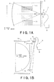
Fig. 1A is a side view showing general construction of a substrate detection apparatus according to one embodiment of this invention together with a FOUP in which a plurality of wafers are stored. -
Fig. 1B is a plane view showing general construction of a substrate detection apparatus according to one embodiment of this invention together with a FOUP in which a plurality of wafers are stored. -
Fig. 2 is a view showing an image obtained by the substrate detection apparatus shown inFigs. 1A and 1B . -
Fig. 3 is a plan view of the substrate detection apparatus according to another embodiment of this invention. -
Fig. 4 is a plan view of the substrate detection apparatus according to one modification of the embodiment shown inFig. 3 . -
Fig. 5 is a side view, for explaining a first example of the present invention, of a cassette storing a plurality of substrates, part of which are in states of inclination and projection. -
Fig. 6 is a view for explaining the first example of the present invention so as to explain a method of judging whether the substrate in the projection state can be processed, or not. -
Fig. 7 is a view for explaining the first example of the present invention so as to explain a method of judging whether the substrate in the inclination state can be processed, or not. -
Fig. 8 is a plane view, for explaining a second example of the present invention, of main components of a substrate detection apparatus. -
Fig. 9 is a plane view, for explaining a third example of the present invention, of main components of a substrate detection apparatus. -
Fig. 10 is a plane view, for explaining a fourth example of the present invention, of main components of a substrate detection apparatus. - Hereinafter, one exemplary substrate detection apparatus according to one embodiment of the present invention and a method using this apparatus will be described with reference to the drawings.
- As shown in
Figs. 1A and 1B , the substrate detection apparatus 1 according to this embodiment is configured for detecting conditions of a plurality ofsemiconductor wafers 11 respectively stored in a FOUP (or wafer cassette) 10. - Each
semiconductor wafer 11 has a flat disk-like shape and is carried in and carried out relative to the FOUP 10 by a hand attached to a distal arm end of a wafer carrier robot. - In the substrate detection apparatus 1, a bright
point light source 2 including a light emitting diode (LED) is provided in a substantially coaxial position relative to animage acquiring means 3 including a CCD camera (or single-lens camera). - The light emitted from the
point light source 2 is radiated toward acollimating reflector 4 including a radiation mirror, and is then collimated by the collimatingreflector 4. - In place of using a proper parabolic mirror, the
collimating reflector 4 may include a curved mirror formed of a plurality of small flat mirrors combined together into a substantially curved surface as a whole. - A
retroreflector 5 is arranged to be opposed to thecollimating reflector 4. Thisretroreflector 5 includes a µ-CCR plate (CCR: Corner Cube Reflector). - The image acquiring means 3 is connected with an image processing means 6 via a transmission cable. Namely, each image obtained by the
image acquiring means 3 will be transmitted to the image processing means 6 via the transmission cable. - In the case of detecting the conditions of the wafers (or substrates) 11 by using the substrate detection apparatus 1 constructed as described above, the light is first radiated from the
point light source 2, and is then reflected and collimated by thecollimating reflector 4. - Thereafter, the light reflected by the
collimating reflector 4 is reflected again, toward thecollimating reflector 4, by theretroreflector 5 arranged to be opposed to the collimating reflector 4 (Illumination step). - As a result, a passing light image including each edge portion of the plurality of
wafers 11 is formed on thecollimating reflector 4 with the light reflected by theretroreflector 4. Namely, in an optical path of the reflected light reflected toward thecollimating reflector 4 by theretroreflector 5, the edge portions of the plurality ofwafers 11 are located, respectively. - Then, the passing light image that is formed on the
collimating reflector 4 and includes the respective edge portions of the plurality ofwafers 11 is acquired by the image acquiring means 3 which includes the CCD camera (Image acquiring step). - As shown in
Fig. 1B , a mirror normal line with respect to thecollimating reflector 4 is arranged, in a plan view, to be parallel with a camera optical axis of the image acquiring means (or CCD camera) 3. Thus, each image of the wafers can be formed to be parallel, relative to one another, in the passing light image. -
Fig. 2 schematically shows the passinglight image 20 formed on thecollimating reflector 4 and obtained by theimage acquiring means 3. - In the passing
light image 20, shades of the respective edge portions of the plurality ofwafers 11 can be seen as a plurality of local shade portions (or low brightness portions). Therefore, with analysis of such a passinglight image 20 by using the image processing means 6, the conditions of the plurality ofwafers 11 stored in thecassette 10 can be detected (Detection step). - More specifically, with analysis of the number of pixels of each shade portion and/or each space between the shade portions, judgment on whether or not the
wafer 11 is present in each slot of thecassette 10, judgment on presence of any double wafer, judgment on presence of any crossing wafer, and/or judgment on presence of any projecting wafer (or amount of projection thereof) can be performed. - Herein, the "double wafer" refers to the case in which two wafers are stored in the same slot while being overlapped relative to each other. The "crossing wafer" refers to the case in which the wafer is stored between left and right slots of different levels. The "projecting wafer" refers to the case in which the wafer is stored in the wafer cassette while projecting forward relative to a preset position.
- In the passing
light image 20 shown inFig. 2 , if the wafer is not present in a certain slot, the shade portion corresponding to this case is lacked. In addition, if the projecting wafer is present, the shade portion corresponding to this case has a greater length in a Y-axial direction, as compared with the other shade portions. Furthermore, if the crossing wafer is present, the shade portion corresponding to this case has a greater width in an X-axial direction, as compared with the other shade portions. Besides, this shade portion is seen over two slots of different levels. Additionally or alternatively, if the double wafer is present, the shade portion corresponding to this case is double the width in the X-axial direction, as compared with the other shade portions. - According to the embodiment having such a feature as described above, various desired effects as described below can be obtained.
- First, this embodiment employs one kind of the image processing method utilizing the camera. In principle, however, this method is somewhat close to a scanning method using a transmission shade sensor. Therefore, this image processing method is less susceptible to the reflectance of each
wafer 11 to be detected, thus providing more reliable detection on the conditions of eachwafer 11 stored in the cassette. - Second, since the passing
light image 20 can be obtained over a certain wide range (in the Y-axial direction) with respect to each edge portion of thewafers 11, the sensor can serve to securely detect the projection of somewafers 11, while serving as the mapping sensor. This effect cannot be obtained by performing the scanning operation only once with the transmission shade sensor of the related art. - Additionally, since each
wafer 11 projecting out from the preset position can be detected from a change in the length in the Y-axial direction of each corresponding shade portion, the amount of projection of thewafer 11 can be readily quantified. - This embodiment can eliminate necessity for the mechanical scanning operation as performed with the conventional transmission shade sensor, thus significantly simplifying the entire system as well as reducing the time required for the detection.
- Furthermore, the detection on the double wafer can be judged from a value of the area of each shade portion, wherein each detected value is markedly changed between the case of the double wafer and the normal case. Therefore, as compared with the related art utilizing each profile of an object, the detection on the double wafer can be performed more securely.
- In addition, since the passing
light image 20 for all of thewafers 11 can be obtained at a time by using the single camera, a significantly small and compact substrate detection apparatus 1 can be achieved. - Next, the
substrate detection apparatus 1A according to another embodiment of this invention will be described, with reference toFig. 3 . - As described above, in the substrate detection apparatus 1 shown in
Figs. 1A and 1B , the light emitted from the pointlight source 2 is first reflected and collimated by thecollimating reflector 4. Then, the collimated light is further reflected by theretroreflector 5. - On the other hand, in the
substrate detection apparatus 1A shown inFig. 3 , a transmissionsurface light source 12 is provided in place of theretroreflector 5 shown inFigs. 1A and 1B , such that the collimated light can be radiated from thesurface light source 12 toward thecollimating reflector 4. - The transmission
surface light source 12 includes anLED light source 13 having LED elements longitudinally arranged in a line therein, and adiffusion transmission plate 14 configured to transmit therethrough the light radiated from the LEDlight source 13. For example, thediffusion transmission plate 14 includes an obscure or frosted glass plate. - Initially, the light just after radiated from the LED
light source 13 is in a relatively uneven state. However, once transmitted through thediffusion transmission plate 14, this light can be changed into a surface light source having a substantially even and homogeneous brightness. - Therefore, also in the case of using the
substrate detection apparatus 1A shown inFig. 3 , the same effect as obtained by the substrate detection apparatus 1 shown inFigs. 1A and 1B can be obtained. Namely, the passing light image that is formed on thecollimating reflector 4 and includes the respective edge portions of the plurality ofwafers 11 can be similarly acquired by using theimage acquiring means 3 including the CCD camera. Then, the so-obtained passing light image can be analyzed in the same manner by using the image processing means 6. -
Fig. 4 shows anothersubstrate detection apparatus 1B according to one modification of the embodiment shown inFig. 3 . In thisapparatus 1B, a reflectionsurface light source 15 is used. - In this reflection surface
light source 15, the light is first radiated from the LEDlight source 13 and then reflected by adiffusion reflector 16. Thus, with this reflection surfacelight source 15, the light can also be radiated toward thecollimating reflector 4, while being in an adequately even and homogeneous state. - Namely, also in the case of using the
substrate detection apparatus 1B shown inFig. 4 , the same effect as presented by the substrate detection apparatus 1 shown inFigs. 1A and 1B can be obtained. - While the present invention has been shown and described with reference to several embodiments thereof, it will be understood that there is no intent to limit the invention by such disclosure, and that various alterations and/or modifications can be made thereto. Namely, from the scope defined by the appended claims, it will be obvious that such alterations and/or modifications should also fall within the technical scope of this invention.
- Some kinds of examples according to the present invention will be described hereunder.
- A First example according to the present invention will be described with reference to
Figs. 5 to 7 . - Generally, the
substrates 11 are transferred by a substrate carrier robot (hereinafter simply called "robot") from one cassette to the other cassette after the conditions of containing thesubstrates 11 in thecassette 10 are detected. - In the past, if the conditions of containing the
substrates 11 are not normal, an operation of robot is stopped in order to prevent a collision between the robot and thesubstrates 11 and/or an abnormal grasping of thesubstrate 11 by the robot. In this case, however, the robot will be stopped even when the containing conditions are slightly deviated from the normal containing conditions. Thereby, there is a problem that the throughput of an entire substrate processing apparatus including the robot will be lowered. - On the other hand, when the conditions of containing the
substrates 11 are detected by the substrate detection apparatus according to the present invention, even if asubstrate 11 is dislocated from a preset position, it can be judged whether thesubstrate 11 can be transferred by correcting some operational parameters, such as operational positions, of the robot. Accordingly, when a transfer of thesubstrate 11 has been judged to be doable, thesubstrate 11 can be transferred by correcting the operational parameters, such as operational positions of the robot, based on the detected values of the containing conditions of thesubstrates 11. - As explained above, the
substrates 11 can be transferred by the robot even in a case that the robot must have been stopped under the conventional art. Thereby, the throughput of the entire substrate processing apparatus including the robot can be improved. - An example of specific process will be mentioned hereunder.
- (1) The conditions of containing the
substrates 11 in thecassette 10 are detected by the substrate detection apparatus according to the present invention. - (2) When a projection of the
substrate 11 has been detected (refer toFig. 5 ), it is judged whether thesubstrate 11 can be grasped by the robot, based on the detected amount of the projection (refer toFig. 6 ). If the grasp of thesubstrate 11 has been judged to be doable, the projectedsubstrate 11 is grasped by the robot by correcting the operational positions of the robot based on the detected amount of the projection. On the other hand, if the grasp of the projectedsubstrate 11 has been judged to be undoable, necessary steps, such as stopping operations, are taken. - (3) When an inclination of the
substrate 11 has been detected (refer toFig. 5 ), it is judged whether the substrate can be grasped by the robot, based on the detected distance between theinclined substrate 11 and asubstrate 11 below the same (refer toFig. 7 ). If the grasp of thesubstrate 11 has been judged to be doable, theinclined substrate 11 is grasped by the robot by correcting the operational parameters, such as operational positions of the robot, based on the detected amount of inclination. On the other hand, if the grasp of theinclined substrate 11 has been judged to be undoable, necessary steps, such as stopping operations, are taken. - (4) When both a projection and an inclination of the
substrate 11 have been detected, a combination of the above-mentioned processes (2) and (3) is performed. - The term "inclination of substrate" is used to mean the state where a substrate within the
cassette 10 has inclined downward with respect to a preset position (refer toFigs. 5 and 6 ). - The criteria for judging whether the robot is able to grasp the
substrate 11 can be appropriately determined according to, for example, the structure of the substrate grasping mechanism of the robot. - A second example according to the present invention will be described with reference to
Fig. 8 . - When there are more than one cassette, the substrate detection apparatus according to the present invention may be applied to each of the cassettes.
- On the other hand, as shown in
Fig. 8 , animage acquiring means 31 and a light source (illumination means) 32 may be disposed on arobot 30 so that the containing conditions of thesubstrates 11 are detected by moving therobot 30 to thecassette 10 to be detected. In this case, one set of the image acquiring means and the light source can be used for more then onecassette 10. Thereby, the apparatus can be made compact and the manufacturing cost thereof can be decreased. - In this example, the light from the
light source 32 mounted on therobot 30 is reflected by adiffusion plate 33 toward the edge portions of thesubstrates 11, and further reflected by areflection plate 34 toward theimage acquiring means 31. - A third example according to the present invention will be described hereunder with reference to
Fig. 9 . - Generally, the
substrates 11 are processed by an automated system, and operators do not always watch the processes performed by the automated system. Therefore, when a failure of substrate transfer by therobot 30 or a collision has occurred, it is usually difficult to determine the cause thereof. - In this regard, by storing the images of the
cassette 10, etc., obtained by the image acquiring means 31 in a storage means 35 (refer toFig. 9 ), it will become possible to analyze the images acquired when an abnormal event, such as a failure of substrate transfer by therobot 30 or a collision, occurred. Thereby, the cause of the abnormal event can be detected, and measures for preventing recurrences of the abnormal event can be examined. - Specifically, images of the
cassette 10, etc., obtained by the image acquiring means 31 of the substrate detection apparatus according to the present invention are stored in the storage means 35 so as to make it possible to refer to images in the past, if necessary. - Only the newest images may be kept remained as long as the storage capacity of the storage means 35 makes it possible, and old images may be deleted (e.g., overwritten). In this regard, deletions (e.g., overwriting) of old images may be stopped when an abnormal event has been detected. Thereby, images acquired within a specific time period before the abnormal event can be kept from being deleted.
- Moreover, the image acquiring means 31 may be mounted on the
robot 30 similar to the second example (refer toFig. 8 ), or at a position other than the robot (refer toFig. 9 ). When theimage acquiring means 31 is mounted on therobot 31, images of the containing conditions of thewafers 11 shown inFig. 5 , etc., can be recorded, and images of any positions can be acquired from any angles by moving therobot 30. In the latter case, angles and positions for taking images can be suitably chosen in order to examine the cause of the abnormal event and measures for preventing recurrences. - When the
image acquiring means 31 is mounted at a position other than the robot, a fixed point observation can be made, regardless of movements of the robot. A moving means and/or a rotating means for the image acquiring means may be disposed. - A fourth example according to the present invention will be described with reference to
Fig. 10 (andFig. 4 ). - In the past, when the
robot 30 is operated to transfer substrates in a state that some slippages have occurred at frictional fastening portions of therobot 30 and/or some deformations of robot members have occurred due to a collision between therobot 30 and an apparatus, etc., therobot 30 may fail to transfer a substrate and/or collide with an apparatus. Moreover, some dedicated detecting means need to be provided in order to detect the above-mentioned slippages and deformations so that the size of apparatus will be enlarged and the costs thereof will be increased. - In this regard, the substrate detection apparatus according to the present invention makes it possible to acquire an image of a specific posture of the
robot 30 in the normal state and store the image in the storage means 35. Then, the stored image of therobot 30 in the normal state can be compared with an image of therobot 30 which is acquired in a state that therobot 30 is controlled to take the specific posture. Thereby, the above-mentioned slippages and deformations can be detected based on the comparison between the image of therobot 30 in the normal state and the image of therobot 30 after use. Moreover, a dedicated detecting means does not need to be provided so that an enlargement of the apparatus and an increase of the costs can be avoided. - An example of a specific process will be described hereunder.
- (1) An image (reference image) of the
robot 30 is acquired by the image acquiring means 3 (refer toFigs. 4 and10 ) in a state that therobot 30 is controlled to take a specific posture in a normal state (refer toFig. 10 ). - (2) The obtained image is stored in the storage means 35.
- (3) When the above-mentioned slippages and deformations of the
robot 30 are to be detected, an image (comparative image) of therobot 30 which is acquired in a state that therobot 30 is controlled to take the specific posture. - (4) The comparative image is compared with the reference image, and it can be determined that some slippages and/or deformations have occurred if there is a difference between the reference image and the comparative image.
- When the comparative image and the reference image are displaced with each other in the vertical directions, it is highly probable that the
hand 36 has been bent and/or some bolts have become loose. On the other hand, when the comparative image and the reference image are displaced with each other in the longitudinal direction of thehand 36, it is highly probable that the driving means of therobot 30 has been deteriorated to produce some positional errors. As explained above, the causes of abnormal events of therobot 30 can be inferred. - The causes of abnormal events may be automatically inferred by a computer so as to display the inferred results. Some thresholds about the differences between comparative images and reference images may be preliminary set, and some slippages and/or deformations are judged to have occurred in the
robot 30 when the differences of comparative/reference images have exceeded the preliminary set thresholds. The above-mentioned judgments can be made about some kinds of differences between comparative images and reference images. For example, the judgments can be made about vertical/horizontal displacements, or each element such as a width of the hand image, or combinations thereof. - Furthermore, operational parameters of the
robot 30 may be corrected based on the results of judgments/comparisons. Thus, therobot 30 can continue the transferring operations even when some displacements and/or deformations have occurred, as long as the transferring operations can be made doable by correcting the operational parameters of therobot 30. As a result, the time period in which therobot 30 is out of service can be decreased. Moreover, more information can be obtained if more than one kinds of postures are used as the above-mentioned specific posture.
Claims (14)
- A substrate detection apparatus adapted for detecting conditions of a plurality of substrates stored in a cassette, comprising:a collimating reflector located on one side of the plurality of substrates;illumination means configured to radiate light in a planar state toward the collimating reflector such that edge portions of the substrates are located in an optical path of the light;image acquiring means configured to acquire a passing light image including the edge portions of the substrates, the passing light image being formed on the collimating reflector with the light radiated in the planar state from the illumination means; andimage processing means configured to process the passing light image obtained by the image acquiring means, thereby detecting the conditions of the substrates stored in the cassette.
- The substrate detection apparatus according to claim 1, wherein the illumination means includes a surface light source.
- The substrate detection apparatus according to claim 1, wherein the illumination means includes a point light source configured to radiate the light toward the collimating reflector, and a retroreflector configured to reflect the light, which has been reflected and collimated by the collimating reflector, toward the collimating reflector.
- The substrate detection apparatus according to claim 3, wherein the point light source and the image acquiring means are arranged substantially coaxially relative to each other.
- The substrate detection apparatus according to any one of claims 2 to 4, wherein the surface light source or the point light source includes a light emitting diode.
- The substrate detection apparatus according to any one of claims 1 to 5, wherein the collimating reflector includes a parabolic mirror.
- The substrate detection apparatus according to any one of claims 1 to 5, wherein the collimating reflector includes a curved mirror formed of a plurality of flat mirrors combined together into a substantially curved surface as a whole.
- A method of detecting conditions of a plurality of substrates stored in a cassette, comprising:an illumination step of radiating light in a planar state from an illumination means toward a collimating reflector located on one side of the substrates such that edge portions of the substrates are located in an optical path of the light;an image acquiring step of taking a passing light image including the edge portions of the substrates by using an image acquiring means, the passing light image being formed on the collimating reflector with the light radiated in the planar state from the illumination means; anda detection step of processing the passing light image obtained by the image acquiring means by using an image processing means, thereby detecting the conditions of the substrates.
- The method of detecting the substrates according to claim 8, wherein the illumination means includes a surface light source.
- The method of detecting the substrates according to claim 8, wherein, in the illumination step, the light is radiated toward the collimating reflector from a point light source, and the light, which has been reflected and collimated by the collimating reflector, is then reflected toward the collimating reflector by a retroreflector with the edge portions of substrates located in the optical path of the light.
- The method of detecting the substrates according to claim 10, wherein the point light source and the image acquiring means are arranged substantially coaxially relative to each other.
- The method of detecting the substrates according to any one of claims 9 to 11, wherein the surface light source or point light source includes a light emitting diode.
- The method of detecting the substrates according to any one of claims 8 to 12, wherein the collimating reflector includes a parabolic mirror.
- The method of detecting the substrates according to any one of claims 8 to 12, wherein the collimating reflector includes a curved mirror formed of a plurality of flat mirrors combined together into a substantially curved surface as a whole.
Applications Claiming Priority (2)
| Application Number | Priority Date | Filing Date | Title |
|---|---|---|---|
| JP2008256268A JP5185756B2 (en) | 2008-10-01 | 2008-10-01 | Substrate detection apparatus and method |
| PCT/JP2009/066938 WO2010038735A1 (en) | 2008-10-01 | 2009-09-29 | Substrate detection device and method |
Publications (3)
| Publication Number | Publication Date |
|---|---|
| EP2346072A1 true EP2346072A1 (en) | 2011-07-20 |
| EP2346072A4 EP2346072A4 (en) | 2012-11-28 |
| EP2346072B1 EP2346072B1 (en) | 2016-05-25 |
Family
ID=42073496
Family Applications (1)
| Application Number | Title | Priority Date | Filing Date |
|---|---|---|---|
| EP09817767.8A Not-in-force EP2346072B1 (en) | 2008-10-01 | 2009-09-29 | Substrate detection device and method |
Country Status (7)
| Country | Link |
|---|---|
| US (1) | US9202732B2 (en) |
| EP (1) | EP2346072B1 (en) |
| JP (1) | JP5185756B2 (en) |
| KR (1) | KR101298791B1 (en) |
| CN (1) | CN102171806B (en) |
| TW (1) | TWI414778B (en) |
| WO (1) | WO2010038735A1 (en) |
Families Citing this family (21)
| Publication number | Priority date | Publication date | Assignee | Title |
|---|---|---|---|---|
| JP5512350B2 (en) * | 2010-03-30 | 2014-06-04 | 川崎重工業株式会社 | Board transfer robot status monitoring device |
| JP5614326B2 (en) * | 2010-08-20 | 2014-10-29 | 東京エレクトロン株式会社 | Substrate transport apparatus, substrate transport method, and recording medium on which program for executing the substrate transport method is recorded |
| JP5333408B2 (en) * | 2010-10-22 | 2013-11-06 | 東京エレクトロン株式会社 | Holding member posture determination apparatus, method thereof, substrate processing apparatus, and storage medium |
| US11880178B1 (en) | 2010-11-16 | 2024-01-23 | Ectoscan Systems, Llc | Surface data, acquisition, storage, and assessment system |
| US9599461B2 (en) * | 2010-11-16 | 2017-03-21 | Ectoscan Systems, Llc | Surface data acquisition, storage, and assessment system |
| TWI484160B (en) * | 2013-04-23 | 2015-05-11 | Au Optronics Corp | A substrate detection device and method |
| JP5750472B2 (en) * | 2013-05-22 | 2015-07-22 | 株式会社安川電機 | Substrate transport robot, substrate transport system, and method for detecting substrate arrangement state |
| CN105206550B (en) * | 2014-06-20 | 2018-08-24 | 北京北方华创微电子装备有限公司 | Reaction chamber and semiconductor equipment |
| CN104916573B (en) * | 2015-06-17 | 2018-07-06 | 北京北方华创微电子装备有限公司 | The silicon chip distribution combined detection method and device of semiconductor equipment bearing area |
| KR101701419B1 (en) * | 2016-08-17 | 2017-02-02 | 주식회사 오토닉스 | Reflective type image detecting sensor |
| US10784134B2 (en) * | 2017-05-03 | 2020-09-22 | Applied Materials, Inc. | Image based substrate mapper |
| EP3706874A4 (en) | 2017-12-06 | 2021-12-29 | Ectoscan Systems, LLC | Performance scanning system and method for improving athletic performance |
| TWI641073B (en) * | 2018-03-09 | 2018-11-11 | 創意電子股份有限公司 | Wafer shipper device |
| JP7346839B2 (en) * | 2019-02-15 | 2023-09-20 | Tdk株式会社 | loading port |
| JP7324667B2 (en) | 2019-09-20 | 2023-08-10 | 株式会社Screenホールディングス | Substrate processing equipment |
| JP7447661B2 (en) * | 2020-04-23 | 2024-03-12 | Tdk株式会社 | Arrangement detection device and load port for plate-shaped objects |
| US12002696B2 (en) * | 2020-06-30 | 2024-06-04 | Brooks Automation Us, Llc | Substrate mapping apparatus and method therefor |
| US11996308B2 (en) * | 2021-03-03 | 2024-05-28 | Taiwan Semiconductor Manufacturing Company, Ltd. | Method for mapping wafers in a wafer carrier |
| JP2023132455A (en) * | 2022-03-11 | 2023-09-22 | シンフォニアテクノロジー株式会社 | Board detection method and load port |
| US12394647B2 (en) * | 2022-09-23 | 2025-08-19 | Taiwan Semiconductor Manufacturing Company, Ltd. | Wafer shift detection |
| TWI900052B (en) * | 2024-06-07 | 2025-10-01 | 鏵友益科技股份有限公司 | Wafer identification device |
Family Cites Families (24)
| Publication number | Priority date | Publication date | Assignee | Title |
|---|---|---|---|---|
| JPS60157230A (en) * | 1984-01-11 | 1985-08-17 | Telmec Co Ltd | Carrying method for semiconductor wafer |
| US4691999A (en) * | 1986-04-04 | 1987-09-08 | Hughes Aircraft Company | Afocal beam expansion apparatus and method |
| JPS63131533A (en) * | 1986-11-21 | 1988-06-03 | Canon Inc | Device and method for detecting oblique substrate |
| JPH03239344A (en) * | 1990-02-17 | 1991-10-24 | Kokusai Electric Co Ltd | Wafer detection apparatus |
| US5225691A (en) * | 1992-05-18 | 1993-07-06 | Avalon Engineering, Inc. | Semiconductor wafer cassette mapper with emitter and detector arrays for slot interrogation |
| JPH06244268A (en) * | 1993-02-16 | 1994-09-02 | Tokyo Electron Tohoku Ltd | Transfer device |
| DE19535871C2 (en) * | 1995-09-27 | 2000-02-10 | Jenoptik Jena Gmbh | Indexer for magazine compartments of a magazine and disc-shaped objects contained therein |
| JPH09283603A (en) * | 1996-04-10 | 1997-10-31 | Metsukusu:Kk | Semiconductor wafer detector |
| JP3977485B2 (en) * | 1997-04-24 | 2007-09-19 | 東京エレクトロン株式会社 | Arm access position detection method and vacuum processing apparatus |
| DE19814046C1 (en) * | 1998-03-30 | 1999-11-18 | Jenoptik Jena Gmbh | Arrangement for the detection of disk-shaped objects in a cassette |
| JP3058615B2 (en) * | 1998-04-10 | 2000-07-04 | 株式会社山武 | Wafer detector |
| JP2001093964A (en) * | 1999-09-21 | 2001-04-06 | Nikon Corp | Wafer detector |
| KR100728414B1 (en) | 2000-12-01 | 2007-06-13 | 웨이퍼마스터스, 인코퍼레이티드 | Wafer Mapping Apparatus and Method |
| JP2003017548A (en) * | 2001-06-28 | 2003-01-17 | Sunx Ltd | Wafer detector |
| US6914233B2 (en) * | 2001-12-12 | 2005-07-05 | Shinko Electric Co., Ltd. | Wafer mapping system |
| JP2003273197A (en) * | 2002-03-14 | 2003-09-26 | Sunx Ltd | Wafer pop-out detection device |
| JP4163435B2 (en) * | 2002-03-29 | 2008-10-08 | 株式会社日本マイクロニクス | Substrate inspection equipment |
| US20040207836A1 (en) * | 2002-09-27 | 2004-10-21 | Rajeshwar Chhibber | High dynamic range optical inspection system and method |
| JP4276440B2 (en) * | 2003-01-06 | 2009-06-10 | 東京エレクトロン株式会社 | Substrate detection method and apparatus, and substrate processing apparatus |
| JP4028814B2 (en) * | 2003-04-21 | 2007-12-26 | 川崎重工業株式会社 | Mapping device |
| JP4196335B2 (en) | 2003-06-10 | 2008-12-17 | 株式会社安川電機 | Thin substrate detection method |
| JP2006170622A (en) * | 2004-12-10 | 2006-06-29 | Olympus Corp | Visual inspection apparatus |
| US8128257B2 (en) * | 2007-02-09 | 2012-03-06 | Bright View Technologies Corporation | Curved compact collimating reflectors |
| CN109255924A (en) * | 2007-11-15 | 2019-01-22 | 爱克斯崔里斯科技有限公司 | particle detection |
-
2008
- 2008-10-01 JP JP2008256268A patent/JP5185756B2/en active Active
-
2009
- 2009-09-29 WO PCT/JP2009/066938 patent/WO2010038735A1/en not_active Ceased
- 2009-09-29 EP EP09817767.8A patent/EP2346072B1/en not_active Not-in-force
- 2009-09-29 US US13/121,498 patent/US9202732B2/en active Active
- 2009-09-29 KR KR1020117007656A patent/KR101298791B1/en not_active Expired - Fee Related
- 2009-09-29 CN CN200980138891.4A patent/CN102171806B/en active Active
- 2009-10-01 TW TW098133411A patent/TWI414778B/en active
Also Published As
| Publication number | Publication date |
|---|---|
| JP2010087340A (en) | 2010-04-15 |
| EP2346072B1 (en) | 2016-05-25 |
| US20110205354A1 (en) | 2011-08-25 |
| EP2346072A4 (en) | 2012-11-28 |
| TWI414778B (en) | 2013-11-11 |
| TW201028679A (en) | 2010-08-01 |
| KR101298791B1 (en) | 2013-08-22 |
| US9202732B2 (en) | 2015-12-01 |
| KR20110049916A (en) | 2011-05-12 |
| WO2010038735A1 (en) | 2010-04-08 |
| CN102171806A (en) | 2011-08-31 |
| CN102171806B (en) | 2014-07-16 |
| JP5185756B2 (en) | 2013-04-17 |
Similar Documents
| Publication | Publication Date | Title |
|---|---|---|
| EP2346072B1 (en) | Substrate detection device and method | |
| JP5512350B2 (en) | Board transfer robot status monitoring device | |
| JP5529522B2 (en) | Substrate storage state detection device and substrate storage state detection method | |
| JP7389695B2 (en) | Wafer transfer device | |
| WO1995019552A1 (en) | A method and apparatus for automatic focusing of a confocal laser microscope | |
| KR20030036897A (en) | Method and apparatus for enhanced embedded substrate inspection through process data collection and substrate imaging techniques | |
| KR100605051B1 (en) | Apparatus, tool and method for visually inspecting an object | |
| KR20010030320A (en) | Apparatus and method for inspecting substrate | |
| CN103033143B (en) | Optical detector | |
| CN110914966A (en) | Method for inspecting containers and inspection system | |
| KR100871495B1 (en) | Method and apparatus for automated process verification and hierarchical board inspection | |
| US8379082B2 (en) | System, methods and apparatus for substrate carrier content verification using a material handling system | |
| JP2009302392A (en) | Substrate detecting device and method | |
| US6356091B1 (en) | Automatic wafer mapping in a wet environment on a wafer cleaner | |
| US6011586A (en) | Low-profile image formation apparatus | |
| WO2002044651A1 (en) | Three dimensional lead inspection system | |
| CN120015660A (en) | Wafer placement status detection method in wafer box and wafer status detection system | |
| JP2010256217A (en) | Shape inspection device and shape inspection method | |
| CN100336166C (en) | Angled sensors for detecting substrates | |
| US20040233322A1 (en) | Camera with improved illuminator | |
| KR100611129B1 (en) | Photoelectric sensor | |
| US20110317003A1 (en) | Method and system for edge inspection using a tilted illumination | |
| US20100012855A1 (en) | Wafer Scanning | |
| JP2009244175A (en) | Light receiving unit of measuring device, light receiving unit of attitude detection sensor, and method for manufacturing the same | |
| CN221926158U (en) | Data transmission port detection device and electronic product detection equipment |
Legal Events
| Date | Code | Title | Description |
|---|---|---|---|
| PUAI | Public reference made under article 153(3) epc to a published international application that has entered the european phase |
Free format text: ORIGINAL CODE: 0009012 |
|
| 17P | Request for examination filed |
Effective date: 20110420 |
|
| AK | Designated contracting states |
Kind code of ref document: A1 Designated state(s): AT BE BG CH CY CZ DE DK EE ES FI FR GB GR HR HU IE IS IT LI LT LU LV MC MK MT NL NO PL PT RO SE SI SK SM TR |
|
| AX | Request for extension of the european patent |
Extension state: AL BA RS |
|
| DAX | Request for extension of the european patent (deleted) | ||
| A4 | Supplementary search report drawn up and despatched |
Effective date: 20121026 |
|
| RIC1 | Information provided on ipc code assigned before grant |
Ipc: H01L 21/67 20060101AFI20121022BHEP |
|
| 17Q | First examination report despatched |
Effective date: 20131129 |
|
| GRAP | Despatch of communication of intention to grant a patent |
Free format text: ORIGINAL CODE: EPIDOSNIGR1 |
|
| INTG | Intention to grant announced |
Effective date: 20151216 |
|
| GRAS | Grant fee paid |
Free format text: ORIGINAL CODE: EPIDOSNIGR3 |
|
| GRAA | (expected) grant |
Free format text: ORIGINAL CODE: 0009210 |
|
| AK | Designated contracting states |
Kind code of ref document: B1 Designated state(s): AT BE BG CH CY CZ DE DK EE ES FI FR GB GR HR HU IE IS IT LI LT LU LV MC MK MT NL NO PL PT RO SE SI SK SM TR |
|
| REG | Reference to a national code |
Ref country code: GB Ref legal event code: FG4D |
|
| REG | Reference to a national code |
Ref country code: CH Ref legal event code: EP |
|
| REG | Reference to a national code |
Ref country code: IE Ref legal event code: FG4D Ref country code: AT Ref legal event code: REF Ref document number: 802957 Country of ref document: AT Kind code of ref document: T Effective date: 20160615 |
|
| REG | Reference to a national code |
Ref country code: DE Ref legal event code: R096 Ref document number: 602009038918 Country of ref document: DE |
|
| REG | Reference to a national code |
Ref country code: FR Ref legal event code: PLFP Year of fee payment: 8 |
|
| REG | Reference to a national code |
Ref country code: LT Ref legal event code: MG4D |
|
| REG | Reference to a national code |
Ref country code: NL Ref legal event code: MP Effective date: 20160525 |
|
| PG25 | Lapsed in a contracting state [announced via postgrant information from national office to epo] |
Ref country code: NO Free format text: LAPSE BECAUSE OF FAILURE TO SUBMIT A TRANSLATION OF THE DESCRIPTION OR TO PAY THE FEE WITHIN THE PRESCRIBED TIME-LIMIT Effective date: 20160825 Ref country code: FI Free format text: LAPSE BECAUSE OF FAILURE TO SUBMIT A TRANSLATION OF THE DESCRIPTION OR TO PAY THE FEE WITHIN THE PRESCRIBED TIME-LIMIT Effective date: 20160525 Ref country code: LT Free format text: LAPSE BECAUSE OF FAILURE TO SUBMIT A TRANSLATION OF THE DESCRIPTION OR TO PAY THE FEE WITHIN THE PRESCRIBED TIME-LIMIT Effective date: 20160525 Ref country code: NL Free format text: LAPSE BECAUSE OF FAILURE TO SUBMIT A TRANSLATION OF THE DESCRIPTION OR TO PAY THE FEE WITHIN THE PRESCRIBED TIME-LIMIT Effective date: 20160525 |
|
| REG | Reference to a national code |
Ref country code: AT Ref legal event code: MK05 Ref document number: 802957 Country of ref document: AT Kind code of ref document: T Effective date: 20160525 |
|
| PG25 | Lapsed in a contracting state [announced via postgrant information from national office to epo] |
Ref country code: LV Free format text: LAPSE BECAUSE OF FAILURE TO SUBMIT A TRANSLATION OF THE DESCRIPTION OR TO PAY THE FEE WITHIN THE PRESCRIBED TIME-LIMIT Effective date: 20160525 Ref country code: GR Free format text: LAPSE BECAUSE OF FAILURE TO SUBMIT A TRANSLATION OF THE DESCRIPTION OR TO PAY THE FEE WITHIN THE PRESCRIBED TIME-LIMIT Effective date: 20160826 Ref country code: HR Free format text: LAPSE BECAUSE OF FAILURE TO SUBMIT A TRANSLATION OF THE DESCRIPTION OR TO PAY THE FEE WITHIN THE PRESCRIBED TIME-LIMIT Effective date: 20160525 Ref country code: SE Free format text: LAPSE BECAUSE OF FAILURE TO SUBMIT A TRANSLATION OF THE DESCRIPTION OR TO PAY THE FEE WITHIN THE PRESCRIBED TIME-LIMIT Effective date: 20160525 Ref country code: ES Free format text: LAPSE BECAUSE OF FAILURE TO SUBMIT A TRANSLATION OF THE DESCRIPTION OR TO PAY THE FEE WITHIN THE PRESCRIBED TIME-LIMIT Effective date: 20160525 Ref country code: PT Free format text: LAPSE BECAUSE OF FAILURE TO SUBMIT A TRANSLATION OF THE DESCRIPTION OR TO PAY THE FEE WITHIN THE PRESCRIBED TIME-LIMIT Effective date: 20160926 |
|
| PG25 | Lapsed in a contracting state [announced via postgrant information from national office to epo] |
Ref country code: RO Free format text: LAPSE BECAUSE OF FAILURE TO SUBMIT A TRANSLATION OF THE DESCRIPTION OR TO PAY THE FEE WITHIN THE PRESCRIBED TIME-LIMIT Effective date: 20160525 Ref country code: SK Free format text: LAPSE BECAUSE OF FAILURE TO SUBMIT A TRANSLATION OF THE DESCRIPTION OR TO PAY THE FEE WITHIN THE PRESCRIBED TIME-LIMIT Effective date: 20160525 Ref country code: DK Free format text: LAPSE BECAUSE OF FAILURE TO SUBMIT A TRANSLATION OF THE DESCRIPTION OR TO PAY THE FEE WITHIN THE PRESCRIBED TIME-LIMIT Effective date: 20160525 Ref country code: CZ Free format text: LAPSE BECAUSE OF FAILURE TO SUBMIT A TRANSLATION OF THE DESCRIPTION OR TO PAY THE FEE WITHIN THE PRESCRIBED TIME-LIMIT Effective date: 20160525 Ref country code: EE Free format text: LAPSE BECAUSE OF FAILURE TO SUBMIT A TRANSLATION OF THE DESCRIPTION OR TO PAY THE FEE WITHIN THE PRESCRIBED TIME-LIMIT Effective date: 20160525 |
|
| PG25 | Lapsed in a contracting state [announced via postgrant information from national office to epo] |
Ref country code: BE Free format text: LAPSE BECAUSE OF NON-PAYMENT OF DUE FEES Effective date: 20160525 Ref country code: SM Free format text: LAPSE BECAUSE OF FAILURE TO SUBMIT A TRANSLATION OF THE DESCRIPTION OR TO PAY THE FEE WITHIN THE PRESCRIBED TIME-LIMIT Effective date: 20160525 Ref country code: PL Free format text: LAPSE BECAUSE OF FAILURE TO SUBMIT A TRANSLATION OF THE DESCRIPTION OR TO PAY THE FEE WITHIN THE PRESCRIBED TIME-LIMIT Effective date: 20160525 Ref country code: AT Free format text: LAPSE BECAUSE OF FAILURE TO SUBMIT A TRANSLATION OF THE DESCRIPTION OR TO PAY THE FEE WITHIN THE PRESCRIBED TIME-LIMIT Effective date: 20160525 |
|
| REG | Reference to a national code |
Ref country code: DE Ref legal event code: R097 Ref document number: 602009038918 Country of ref document: DE |
|
| PLBE | No opposition filed within time limit |
Free format text: ORIGINAL CODE: 0009261 |
|
| STAA | Information on the status of an ep patent application or granted ep patent |
Free format text: STATUS: NO OPPOSITION FILED WITHIN TIME LIMIT |
|
| PG25 | Lapsed in a contracting state [announced via postgrant information from national office to epo] |
Ref country code: MC Free format text: LAPSE BECAUSE OF FAILURE TO SUBMIT A TRANSLATION OF THE DESCRIPTION OR TO PAY THE FEE WITHIN THE PRESCRIBED TIME-LIMIT Effective date: 20160525 |
|
| REG | Reference to a national code |
Ref country code: CH Ref legal event code: PL |
|
| 26N | No opposition filed |
Effective date: 20170228 |
|
| PG25 | Lapsed in a contracting state [announced via postgrant information from national office to epo] |
Ref country code: SI Free format text: LAPSE BECAUSE OF FAILURE TO SUBMIT A TRANSLATION OF THE DESCRIPTION OR TO PAY THE FEE WITHIN THE PRESCRIBED TIME-LIMIT Effective date: 20160525 |
|
| REG | Reference to a national code |
Ref country code: IE Ref legal event code: MM4A |
|
| PG25 | Lapsed in a contracting state [announced via postgrant information from national office to epo] |
Ref country code: IE Free format text: LAPSE BECAUSE OF NON-PAYMENT OF DUE FEES Effective date: 20160929 Ref country code: LI Free format text: LAPSE BECAUSE OF NON-PAYMENT OF DUE FEES Effective date: 20160930 Ref country code: CH Free format text: LAPSE BECAUSE OF NON-PAYMENT OF DUE FEES Effective date: 20160930 |
|
| REG | Reference to a national code |
Ref country code: FR Ref legal event code: PLFP Year of fee payment: 9 |
|
| PG25 | Lapsed in a contracting state [announced via postgrant information from national office to epo] |
Ref country code: LU Free format text: LAPSE BECAUSE OF NON-PAYMENT OF DUE FEES Effective date: 20160929 |
|
| PG25 | Lapsed in a contracting state [announced via postgrant information from national office to epo] |
Ref country code: CY Free format text: LAPSE BECAUSE OF FAILURE TO SUBMIT A TRANSLATION OF THE DESCRIPTION OR TO PAY THE FEE WITHIN THE PRESCRIBED TIME-LIMIT Effective date: 20160525 Ref country code: HU Free format text: LAPSE BECAUSE OF FAILURE TO SUBMIT A TRANSLATION OF THE DESCRIPTION OR TO PAY THE FEE WITHIN THE PRESCRIBED TIME-LIMIT; INVALID AB INITIO Effective date: 20090929 |
|
| PG25 | Lapsed in a contracting state [announced via postgrant information from national office to epo] |
Ref country code: IS Free format text: LAPSE BECAUSE OF FAILURE TO SUBMIT A TRANSLATION OF THE DESCRIPTION OR TO PAY THE FEE WITHIN THE PRESCRIBED TIME-LIMIT Effective date: 20160525 Ref country code: MK Free format text: LAPSE BECAUSE OF FAILURE TO SUBMIT A TRANSLATION OF THE DESCRIPTION OR TO PAY THE FEE WITHIN THE PRESCRIBED TIME-LIMIT Effective date: 20160525 Ref country code: TR Free format text: LAPSE BECAUSE OF FAILURE TO SUBMIT A TRANSLATION OF THE DESCRIPTION OR TO PAY THE FEE WITHIN THE PRESCRIBED TIME-LIMIT Effective date: 20160525 Ref country code: MT Free format text: LAPSE BECAUSE OF NON-PAYMENT OF DUE FEES Effective date: 20160930 |
|
| PG25 | Lapsed in a contracting state [announced via postgrant information from national office to epo] |
Ref country code: BG Free format text: LAPSE BECAUSE OF FAILURE TO SUBMIT A TRANSLATION OF THE DESCRIPTION OR TO PAY THE FEE WITHIN THE PRESCRIBED TIME-LIMIT Effective date: 20160525 |
|
| REG | Reference to a national code |
Ref country code: FR Ref legal event code: PLFP Year of fee payment: 10 |
|
| PGFP | Annual fee paid to national office [announced via postgrant information from national office to epo] |
Ref country code: DE Payment date: 20240806 Year of fee payment: 16 |
|
| PGFP | Annual fee paid to national office [announced via postgrant information from national office to epo] |
Ref country code: GB Payment date: 20240808 Year of fee payment: 16 |
|
| PGFP | Annual fee paid to national office [announced via postgrant information from national office to epo] |
Ref country code: FR Payment date: 20240808 Year of fee payment: 16 |
|
| PGFP | Annual fee paid to national office [announced via postgrant information from national office to epo] |
Ref country code: IT Payment date: 20240812 Year of fee payment: 16 |
|
| REG | Reference to a national code |
Ref country code: DE Ref legal event code: R079 Ref document number: 602009038918 Country of ref document: DE Free format text: PREVIOUS MAIN CLASS: H01L0021670000 Ipc: H10P0072000000 |
|
| REG | Reference to a national code |
Ref country code: DE Ref legal event code: R119 Ref document number: 602009038918 Country of ref document: DE |
|
| GBPC | Gb: european patent ceased through non-payment of renewal fee |
Effective date: 20250929 |
|
| PG25 | Lapsed in a contracting state [announced via postgrant information from national office to epo] |
Ref country code: GB Free format text: LAPSE BECAUSE OF NON-PAYMENT OF DUE FEES Effective date: 20250929 |
|
| PG25 | Lapsed in a contracting state [announced via postgrant information from national office to epo] |
Ref country code: IT Free format text: LAPSE BECAUSE OF NON-PAYMENT OF DUE FEES Effective date: 20250929 |
|
| PG25 | Lapsed in a contracting state [announced via postgrant information from national office to epo] |
Ref country code: DE Free format text: LAPSE BECAUSE OF NON-PAYMENT OF DUE FEES Effective date: 20260401 |
|
| PG25 | Lapsed in a contracting state [announced via postgrant information from national office to epo] |
Ref country code: FR Free format text: LAPSE BECAUSE OF NON-PAYMENT OF DUE FEES Effective date: 20250930 |