EP2343188A1 - Liquid ejecting head and liquid ejecting apparatus - Google Patents
Liquid ejecting head and liquid ejecting apparatus Download PDFInfo
- Publication number
- EP2343188A1 EP2343188A1 EP11150067A EP11150067A EP2343188A1 EP 2343188 A1 EP2343188 A1 EP 2343188A1 EP 11150067 A EP11150067 A EP 11150067A EP 11150067 A EP11150067 A EP 11150067A EP 2343188 A1 EP2343188 A1 EP 2343188A1
- Authority
- EP
- European Patent Office
- Prior art keywords
- piezoelectric
- piezoelectric layer
- electrode
- liquid ejecting
- film
- Prior art date
- Legal status (The legal status is an assumption and is not a legal conclusion. Google has not performed a legal analysis and makes no representation as to the accuracy of the status listed.)
- Granted
Links
Images







Classifications
-
- B—PERFORMING OPERATIONS; TRANSPORTING
- B41—PRINTING; LINING MACHINES; TYPEWRITERS; STAMPS
- B41J—TYPEWRITERS; SELECTIVE PRINTING MECHANISMS, i.e. MECHANISMS PRINTING OTHERWISE THAN FROM A FORME; CORRECTION OF TYPOGRAPHICAL ERRORS
- B41J2/00—Typewriters or selective printing mechanisms characterised by the printing or marking process for which they are designed
- B41J2/005—Typewriters or selective printing mechanisms characterised by the printing or marking process for which they are designed characterised by bringing liquid or particles selectively into contact with a printing material
- B41J2/01—Ink jet
- B41J2/135—Nozzles
- B41J2/14—Structure thereof only for on-demand ink jet heads
- B41J2/14201—Structure of print heads with piezoelectric elements
- B41J2/14233—Structure of print heads with piezoelectric elements of film type, deformed by bending and disposed on a diaphragm
-
- H—ELECTRICITY
- H10—SEMICONDUCTOR DEVICES; ELECTRIC SOLID-STATE DEVICES NOT OTHERWISE PROVIDED FOR
- H10N—ELECTRIC SOLID-STATE DEVICES NOT OTHERWISE PROVIDED FOR
- H10N30/00—Piezoelectric or electrostrictive devices
- H10N30/20—Piezoelectric or electrostrictive devices with electrical input and mechanical output, e.g. functioning as actuators or vibrators
- H10N30/204—Piezoelectric or electrostrictive devices with electrical input and mechanical output, e.g. functioning as actuators or vibrators using bending displacement, e.g. unimorph, bimorph or multimorph cantilever or membrane benders
- H10N30/2047—Membrane type
-
- H—ELECTRICITY
- H10—SEMICONDUCTOR DEVICES; ELECTRIC SOLID-STATE DEVICES NOT OTHERWISE PROVIDED FOR
- H10N—ELECTRIC SOLID-STATE DEVICES NOT OTHERWISE PROVIDED FOR
- H10N30/00—Piezoelectric or electrostrictive devices
- H10N30/704—Piezoelectric or electrostrictive devices based on piezoelectric or electrostrictive films or coatings
-
- H—ELECTRICITY
- H10—SEMICONDUCTOR DEVICES; ELECTRIC SOLID-STATE DEVICES NOT OTHERWISE PROVIDED FOR
- H10N—ELECTRIC SOLID-STATE DEVICES NOT OTHERWISE PROVIDED FOR
- H10N30/00—Piezoelectric or electrostrictive devices
- H10N30/80—Constructional details
- H10N30/85—Piezoelectric or electrostrictive active materials
- H10N30/853—Ceramic compositions
- H10N30/8548—Lead-based oxides
- H10N30/8554—Lead-zirconium titanate [PZT] based
-
- B—PERFORMING OPERATIONS; TRANSPORTING
- B41—PRINTING; LINING MACHINES; TYPEWRITERS; STAMPS
- B41J—TYPEWRITERS; SELECTIVE PRINTING MECHANISMS, i.e. MECHANISMS PRINTING OTHERWISE THAN FROM A FORME; CORRECTION OF TYPOGRAPHICAL ERRORS
- B41J2/00—Typewriters or selective printing mechanisms characterised by the printing or marking process for which they are designed
- B41J2/005—Typewriters or selective printing mechanisms characterised by the printing or marking process for which they are designed characterised by bringing liquid or particles selectively into contact with a printing material
- B41J2/01—Ink jet
- B41J2/135—Nozzles
- B41J2/14—Structure thereof only for on-demand ink jet heads
- B41J2/14201—Structure of print heads with piezoelectric elements
- B41J2/14233—Structure of print heads with piezoelectric elements of film type, deformed by bending and disposed on a diaphragm
- B41J2002/14241—Structure of print heads with piezoelectric elements of film type, deformed by bending and disposed on a diaphragm having a cover around the piezoelectric thin film element
-
- B—PERFORMING OPERATIONS; TRANSPORTING
- B41—PRINTING; LINING MACHINES; TYPEWRITERS; STAMPS
- B41J—TYPEWRITERS; SELECTIVE PRINTING MECHANISMS, i.e. MECHANISMS PRINTING OTHERWISE THAN FROM A FORME; CORRECTION OF TYPOGRAPHICAL ERRORS
- B41J2/00—Typewriters or selective printing mechanisms characterised by the printing or marking process for which they are designed
- B41J2/005—Typewriters or selective printing mechanisms characterised by the printing or marking process for which they are designed characterised by bringing liquid or particles selectively into contact with a printing material
- B41J2/01—Ink jet
- B41J2/135—Nozzles
- B41J2/14—Structure thereof only for on-demand ink jet heads
- B41J2002/14419—Manifold
-
- H—ELECTRICITY
- H10—SEMICONDUCTOR DEVICES; ELECTRIC SOLID-STATE DEVICES NOT OTHERWISE PROVIDED FOR
- H10N—ELECTRIC SOLID-STATE DEVICES NOT OTHERWISE PROVIDED FOR
- H10N30/00—Piezoelectric or electrostrictive devices
- H10N30/01—Manufacture or treatment
- H10N30/07—Forming of piezoelectric or electrostrictive parts or bodies on an electrical element or another base
- H10N30/074—Forming of piezoelectric or electrostrictive parts or bodies on an electrical element or another base by depositing piezoelectric or electrostrictive layers, e.g. aerosol or screen printing
- H10N30/077—Forming of piezoelectric or electrostrictive parts or bodies on an electrical element or another base by depositing piezoelectric or electrostrictive layers, e.g. aerosol or screen printing by liquid phase deposition
- H10N30/078—Forming of piezoelectric or electrostrictive parts or bodies on an electrical element or another base by depositing piezoelectric or electrostrictive layers, e.g. aerosol or screen printing by liquid phase deposition by sol-gel deposition
-
- H—ELECTRICITY
- H10—SEMICONDUCTOR DEVICES; ELECTRIC SOLID-STATE DEVICES NOT OTHERWISE PROVIDED FOR
- H10N—ELECTRIC SOLID-STATE DEVICES NOT OTHERWISE PROVIDED FOR
- H10N30/00—Piezoelectric or electrostrictive devices
- H10N30/01—Manufacture or treatment
- H10N30/08—Shaping or machining of piezoelectric or electrostrictive bodies
- H10N30/082—Shaping or machining of piezoelectric or electrostrictive bodies by etching, e.g. lithography
Definitions
- the present invention relates to a liquid ejecting head which ejects liquid from nozzle openings and a liquid ejecting apparatus.
- a piezoelectric element used in a liquid ejecting head there is a piezoelectric element which is configured by interposing between two electrodes a piezoelectric layer formed of a piezoelectric material having an electromechanical conversion function, for example, a crystallized dielectric material.
- a piezoelectric element is mounted in a liquid ejecting head as, for example, an actuator device of a flexural vibration mode.
- a liquid ejecting head for example, there is an ink jet recording head wherein a part of a pressure generating chamber, which communicates with nozzle openings which discharge ink, is configured by a vibrating plate, and the vibrating plate is deformed by a piezoelectric element to pressurize ink in the pressure generating chamber, thus discharging ink droplets from the nozzle openings.
- the piezoelectric element mounted in such an ink jet recording head for example, there is the piezoelectric element formed so as to be independent for each pressure generating chamber by forming a uniform piezoelectric material layer using film deposition technology over the entire surface of the vibrating plate, and cutting the piezoelectric material layer into shapes corresponding to the pressure generating chambers using a lithographic method (refer to JP-A-2003-127366 ).
- the piezoelectric layer In the piezoelectric element, stress acts on the piezoelectric layer when a voltage is applied, and when this happens, there is a problem in that cracks may be generated in the piezoelectric layer.
- a thin film deposition method such as a solution deposition technique or a CVD method, which is different to a so-called bulk piezoelectric layer formed by sintering grains of metal oxide
- the problem of the generation of cracks becomes pronounced due to stress acting on the piezoelectric element becoming large.
- a problem such as this is not limited to ink jet recording heads and also occurs in liquid ejecting heads which eject other liquids.
- An advantage of some aspects of the invention is that there is provided a liquid ejecting head, which suppresses the generation of cracks in a piezoelectric layer, and a liquid ejecting apparatus.
- a liquid ejecting head including pressure generating chambers which communicate with nozzle openings, and a piezoelectric element which generates changes in pressure in the pressure generating chambers and which is provided with a first electrode, a piezoelectric layer which contains lead, zirconium, and titanium, and is formed on the first electrode, a second electrode formed on the opposite side of the piezoelectric layer to the first electrode, wherein a groove portion, which exists between grains in the second electrode side surface of the piezoelectric layer, satisfies 0 ⁇ d/ ⁇ 0.900 (where d: depth of groove, w: width of groove, p: radius of curvature (d 2 +w 2 /4)/2d).
- the generation of cracks in the piezoelectric layer when a voltage is applied can be suppressed, and a liquid ejecting head has superior durability.
- the thickness of the piezoelectric layer may be 6 ⁇ m or less. It is easier for cracks to be generated as the thickness of the piezoelectric layer becomes thinner due to larger stress acting on the piezoelectric layer. However, according to this configuration, even with a thin piezoelectric layer of 6 ⁇ m or less, the generation of cracks can be suppressed.
- a liquid ejecting apparatus including the liquid ejecting head of the aspect described above. According to the present aspect, it is possible to realize a liquid ejecting apparatus which includes a liquid ejecting head with a piezoelectric element which suppresses the generation of cracks in the piezoelectric layer.
- Fig. 1 is an exploded perspective diagram illustrating a schematic configuration of a recording head according to a first embodiment of the invention.
- Figs. 2A and 2B are respectively a planar diagram and a cross sectional diagram of the recording head according to the first embodiment of the invention.
- Fig. 3 is an enlarged cross sectional diagram of main sections of the recording head according to the first embodiment of the invention.
- Fig. 4 is an enlarged cross sectional diagram of main sections of a piezoelectric layer.
- Figs. 5A and 5B are cross sectional diagrams illustrating manufacturing processes of the recording head according to the first embodiment of the invention.
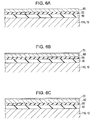
- Figs. 6A to 6C are cross sectional diagrams illustrating manufacturing processes of the recording head according to the first embodiment of the invention.
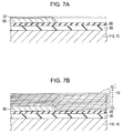
- Figs. 7A and 7B are cross sectional diagrams illustrating manufacturing processes of the recording head according to the first embodiment of the invention.
- Figs. 8A to 8C are cross sectional diagrams illustrating manufacturing processes of the recording head according to the first embodiment of the invention.
- Figs. 9A and 9B are cross sectional diagrams illustrating manufacturing processes of the recording head according to the first embodiment of the invention.
- Fig. 10 is an AFM image of a piezoelectric layer of a piezoelectric element A.
- Fig. 11 is an AFM image of a piezoelectric layer of a piezoelectric element B.
- Fig. 12 is an AFM image of a piezoelectric layer of a piezoelectric element C.
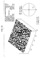
- Fig. 13 is an AFM image of a piezoelectric layer of a piezoelectric element D.
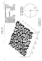
- Fig. 14 is an AFM image of a piezoelectric layer of a piezoelectric element E.
- Fig. 15 is a graph illustrating an example of a measurement result of a groove portion of the piezoelectric layer of the piezoelectric element A.
- Fig. 16 is a graph illustrating results of generation rates of cracks.
- Fig. 17 is a graph illustrating a relationship between a period of voltage application and breakage generating stress in a piezoelectric layer.
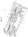
- Fig. 18 is a diagram illustrating a schematic configuration of a recording apparatus according to an embodiment of the invention.
- Fig. 1 is an exploded perspective diagram illustrating a schematic configuration of an ink jet recording head which is an example of a liquid ejecting head according to a first embodiment of the invention.
- Fig. 2A is a planar diagram of Fig. 1 and Fig. 2B is a cross sectional diagram taken along line IIB-IIB of Fig. 1 .
- Fig. 3 is a cross sectional diagram which enlarges main sections of the ink jet recording head.
- a flow path forming substrate 10 of the embodiment is formed from a single crystal silicon substrate, and on one surface thereof, an elastic film 50 is formed from silicon dioxide.
- a plurality of pressure generating chambers 12 is arranged in a line in the width direction thereof. Also, in a region on the outside in the longitudinal direction of the pressure generating chamber 12 of the flow path forming substrate 10, a communication section 13 is formed.
- the communication section 13 and each of the pressure generating chambers 12 communicate via ink supply paths 14 and communication paths 15 provided for each of the pressure generating chambers 12.
- the communication section 13 communicates with a reservoir section 31 of a protective substrate which will be described later, and configures a part of a reservoir which is an ink chamber shared by each of the pressure generating chambers 12.
- the ink supply paths 14 are formed with a width narrower than that of the pressure generating chambers 12 and maintain a constant flow path resistance with regard to ink flowing into the pressure generating chambers 12 from the communication section 13.
- the ink supply paths 14 are formed by narrowing the width of the flow path from one side.
- the ink supply paths may be formed by narrowing the width of the flow path from both sides.
- the ink supply paths may be formed, not by narrowing the width of the flow path, but by narrowing in the thickness direction.
- a liquid flow path is provided which is formed of the pressure generating chambers 12, the communication section 13, the ink supply paths 14 and the communication paths 15.
- a nozzle plate 20 which is provided with nozzle openings 21 which communicate with the vicinity of the edge portion of each of the pressure generating chambers 12 on the side opposite to the ink supply paths 14, is attached by an adhesive, a heat adhesion film or the like.
- the nozzle plate 20 is formed of, for example, glass ceramics, a silicon single crystal substrate, stainless steel or the like.
- the elastic film 50 described above is formed, and on the elastic film 50, an insulating film 55 is formed. Furthermore, on the insulating film 55, a laminated layer is formed of a first electrode 60 formed of platinum, iridium or the like, a piezoelectric layer 70 formed in a thin film with a thickness of 6 ⁇ m or less, or more preferably, a thickness of 0.3 ⁇ m to 1.5 ⁇ m, and a second electrode 80 formed of iridium or the like, and this configures a piezoelectric element 300.
- the piezoelectric element 300 is a portion including the first electrode 60, the piezoelectric layer 70 and the second electrode 80.
- any one of the electrodes of the piezoelectric element 300 is configured as a common electrode, and the other electrode and the piezoelectric layer 70 are configured by being patterned for each of the pressure generating chambers 12.
- the first electrode 60 is the common electrode of the piezoelectric element 300
- the second electrode 80 is the individual electrode of the piezoelectric element 300.
- the combination of the piezoelectric element 300 and a vibrating plate displaced by the driving of the piezoelectric element 300 is referred to as an actuator device.
- the elastic film 50, the insulating film 55 and the first electrode 60 function as the vibrating plate, but the vibrating plate is of course not limited to this, and for example, the elastic film 50 and the insulating film 55 may be not provided, and just the first electrode 60 may function as the vibrating plate. Also, the piezoelectric element 300 itself may function as the vibrating plate in practice.
- the piezoelectric layer 70 is formed on the first electrode 60 from a piezoelectric material showing an electromechanical conversion function, in particular, from among piezoelectric materials, a ferroelectric material which has a perovskite structure and contains Pb, Zr and Ti as metals.
- a ferroelectric material such as lead zirconate titanate (PZT) or a material, where metal oxide such as niobium oxide, nickel oxide, magnesium oxide, or the like is added, is preferable as the piezoelectric layer 70.
- lead zirconate titanate (Pb(Zr, Ti)O 3 ), lead lanthanum zirconate titanate ((Pb, La)(Zr, Ti)O 3 ), lead magnesium niobate - lead zirconate titanate (Pb(Zr, Ti) (Mg, Nb)O 3 ) and the like can be used.
- a plurality of grains 501 are formed with column shapes continuous in the thickness direction of the piezoelectric layer 70.
- a grain refers to a crystal region with the same crystalline orientation.
- Fig. 4 which is an enlarged cross sectional diagram of the piezoelectric layer 70
- the plurality of grains 501 exist in the surface on the second electrode 80 side of the piezoelectric layer 70, and as the grain 501 is typically not formed to have no gap with the adjacent grain 501 up to the surface, a groove portion 502 is formed which is indented from the surface of the piezoelectric layer 70 due to the adjacent grains 501.
- the groove portion 502 satisfies 0 ⁇ d/ ⁇ 0.900.
- d is the depth of the groove portion 502
- w is the width of the groove portion 502
- p is the radius of curvature, that is, (d 2 +w 2 /4)/2d.
- the method of measuring the depth d and the width w of the groove portion 502 is not particularly limited and an atom force microscope (AFM) or a scanning probe microscope (SPM) can be used, for example, for the measuring by the conditions described below.
- AFM atom force microscope
- SPM scanning probe microscope
- the depth d and the width w are measured by setting the average value of the height in the thickness direction to zero in the measurement range, and the zero of the flat surface is used as a reference.
- Nanoscope III manufactured by Digital Instruments Inc.
- AFM tip NCH (tip shape: PointProbe with length of 125 ⁇ m, spring constant of 42 N/m, resonance frequency of 320 kHz)
- Measurement mode AC mode (tapping mode) Measurement range: 5 ⁇ m ⁇ 5 ⁇ m Measurement resolution: 1064 ⁇ 1064
- the plurality of the groove portions 502 are formed in the second electrode 80 side surface of the piezoelectric layer 70, it is sufficient if the averaged value of d/ ⁇ of each of the groove portions 502 satisfies 0 ⁇ d/ ⁇ 0.900.
- the region in the piezoelectric layer 70, where there is significant stress when a voltage is applied is not limited to the groove portions 502 formed between the grains 501 in the second electrode 80 side surface, but several such regions exist, such as at grooves formed between the adjacent grains 501 and the like on the first electrode 60 side surface of the piezoelectric layer 70, low density portions which are caused by unevenness in ceramics, typical points which appear in a burning interface in the liquid layer process, and the like.
- the generation of cracks in the piezoelectric layer 70 is hardly influenced by the grooves formed between the adjacent grains 501 and the like on the first electrode 60 side surface of the piezoelectric layer 70, the low density portions which are caused by unevenness in ceramics, the typical points which appear in a burning interface in the liquid layer process, and the like. It has been found that the generation of cracks depends on the groove portions 502 formed between the grains 501 in the second electrode 80 side surface of the piezoelectric layer 70.
- the piezoelectric layer is formed as a thin film using a thin film forming method such as a solution technique or a CVD method, which is different to a so-called bulk (thick film) piezoelectric layer formed by sintering grains of metal oxide, it becomes easy for cracks to be generated as considerable stress acts on the piezoelectric layer 70 compared to a thick film when a voltage is applied.
- a thin film forming method such as a solution technique or a CVD method
- the groove portions 502 which exist between the grains 501 in the second electrode 80 side surface of the piezoelectric layer 70 satisfy 0 ⁇ d/ ⁇ 0.900, even with the thin piezoelectric layer 70 with a thickness of 6 ⁇ m, the generation of cracks can be suppressed and the ink jet recording head has superior durability.
- a lead electrode 90 is connected which is formed of, for example, gold (Au) or the like, and is drawn out from the vicinity of the edge portion of the ink supply path 14 side to extend to above the insulating film 55.
- a protective substrate 30 which has the reservoir section 31 which configures at least a part of a reservoir 100, is bonded via an adhesive 35.
- the reservoir section 31 penetrates through the protective substrate 30 in the thickness direction and is formed to span over the width direction of the pressure generating chambers 12.
- the reservoir section 31 communicates with the communication section 13 of the flow path forming substrate 10, and configures the reservoir 100 which is an ink chamber shared by each of the pressure generating chambers 12.
- the communication section 13 of the flow path forming substrate 10 may be divided into a plurality for each of the pressure generating chambers 12 and only the reservoir section 31 may function as the reservoir. Furthermore, for example, only the pressure generating chambers 12 may be provided in the flow path forming substrate 10, and ink supply paths 14 may be provided in a member (such as the elastic film 50, the insulating film 55 and the like) interposed between the flow path forming substrate 10 and the protective substrate 30 so as to communicate with each of the pressure generating chambers 12 and the reservoir.
- a member such as the elastic film 50, the insulating film 55 and the like
- a piezoelectric element holding section 32 which has a gap so that movement of the piezoelectric element 300 is not hindered. It is sufficient if the piezoelectric element holding section 32 has a gap so that movement of the piezoelectric element 300 is not hindered, and the gap may or may not be tightly sealed.
- the protective substrate 30 it is preferable to use a material with substantially the same rate of thermal expansion as the flow path forming substrate 10, for example, glass, a ceramic material or the like, and in the embodiment, to form the protective substrate 30, a single crystal silicon substrate is used which is the same material as for the flow path forming substrate 10.
- a through hole 33 is provided which passes through the protective substrate 30 in the thickness direction.
- the vicinity of the edge portion of the lead electrodes 90, which are drawn out from each of the piezoelectric elements 300, is arranged so as to be exposed in the through hole 33.
- a driving circuit 120 is fixed in order to drive the piezoelectric elements 300 which are arranged in a line.
- the driving circuit 120 for example, a circuit substrate, a semiconductor integrated circuit (IC) or the like can be used.
- the driving circuit 120 and the lead electrode 90 are electrically connected via connection wiring formed of conductive wire such as a bonding wire 121.
- a compliance substrate 40 is bonded which is formed from a sealing film 41 and a fixing substrate 42.
- the sealing film 41 is formed from a material with low rigidity and flexibility, and one surface of the reservoir portion 31 is sealed by the sealing film 41.
- the fixing substrate 42 is formed from a comparatively hard material. Since a region of the fixing substrate 42 opposing the reservoir 100 becomes an opening section 43 which has been completely removed in the thickness direction, one surface of the reservoir 100 is sealed only by the sealing film 41 having flexibility.
- ink jet recording head I of the embodiment after ink is input from an ink introduction port connected to an external ink supply means (not shown) and the inside is filled up by ink from the reservoir 100 until it reaches the nozzle openings 21, a voltage is applied between each of the first electrodes 60 and the second electrodes 80 which correspond to the pressure generating chambers 12, according to recording signals from the driving circuit 120, and due to the elastic film 50, the insulating film 55, the first electrode 60 and the piezoelectric layer 70 bending and deforming, the pressure inside each of the pressure generating chambers 12 is increased, thereby ink droplets are discharged from the nozzle openings 21.
- a voltage of 35 V which is the voltage typically used for ink jet recording heads, effective driving can be performed at 35 V or less and the liquid ejecting head is reliable.
- FIGS. 5A to 9B are cross sectional diagrams of the pressure generating chamber in the longitudinal direction.
- a silicon dioxide film is formed from silicon dioxide (SiO 2 ) or the like which configures the elastic film 50 on the surface of the flow path forming substrate wafer 110 which is a silicon wafer.
- the insulating film 55 is formed from zirconium oxide or the like by reactive sputtering, thermal oxidation or the like.
- the first electrode 60 is formed over the entire surface of the insulating film 55 from platinum, iridium or the like using DC sputtering or the like.
- the piezoelectric layer 70 is laminated over the entire upper surface of the first electrode 60.
- the manufacturing method of the piezoelectric layer 70 is not particularly limited as long as it is a so-called thin film forming method where a thin film of the piezoelectric layer 70 can be formed.
- the piezoelectric layer 70 can be formed using an MOD (metal-organic decomposition) method where a solution formed by dissolving and dispersing a metal-organic compound in a solvent is applied and dried and is then burned at a high temperature to obtain the piezoelectric layer 70 formed of a metal oxide.
- MOD metal-organic decomposition
- the manufacturing method of the piezoelectric layer 70 is not limited to an MOD method, and for example, a sol-gel method, a laser ablation method, a sputtering method, a pulsed laser deposition (PLD) method, a CVD method, an aerosol deposition method and the like may be used, and a liquid phase deposition method or a solid phase deposition method may be used.
- a sol-gel method for example, a laser ablation method, a sputtering method, a pulsed laser deposition (PLD) method, a CVD method, an aerosol deposition method and the like may be used, and a liquid phase deposition method or a solid phase deposition method may be used.
- a piezoelectric precursor film 71 is formed (coating process) by coating an MOD solution or a Sol (precursor solution), which contains a metal-organic compound, specifically, a metal-organic compound containing lead, zirconium, and titanium in a predetermined ratio, using a spin coating method or the like.
- the precursor solution for coating mixes a metal-organic compound containing each of lead, zirconium, and titanium, and this mixture is made into a solution or a dispersion using an organic solvent such as alcohol.
- an organic solvent such as alcohol.
- the metal-organic compound containing each of lead, zirconium, and titanium for example, metal alkoxide, an organic acid salt, a ⁇ -diketone complex or the like can be used.
- the piezoelectric precursor film 71 is heated to a predetermined temperature and dried for a specific period (drying process).
- the dried piezoelectric precursor film 71 is degreased by being heated to and held at a predetermined temperature for a specific period of time (degreasing process).
- the degreasing used here is a discharging of organic components contained in the piezoelectric precursor film 71 as, for example, NO 2 , CO 2 , H 2 O and the like.
- the atmosphere during the drying process and the degreasing process is not limited, and performing the process may be carried out in air or inert gas.
- the piezoelectric precursor film 71 is crystallized by being heated to and held at a predetermined temperature, such as approximately 600 to 800°C, for a specific period in an inert gas atmosphere, to form a piezoelectric film 72 (burning process).
- a predetermined temperature such as approximately 600 to 800°C
- the heating device used in the drying process for example, an RTA (Rapid Thermal Annealing) device which heats using irradiation of an infrared lamp, a hot plate or the like can be used.
- RTA Rapid Thermal Annealing
- the first electrode 60 and the first layer of the piezoelectric film 72 are simultaneously patterned so that their side surfaces are inclined with a resist (not shown) with a predetermined shape on the piezoelectric film 72 as a mask.
- the piezoelectric layer 70 is formed from a plurality of the piezoelectric films 72 using the above described coating process, drying process, and degreasing process or the coating process, drying process, degreasing process and burning process being repeated plural times according to a predetermined thickness and the like.
- the piezoelectric layer 70 with a predetermined thickness is formed from a plurality of layers of the piezoelectric film 72.
- the film thickness is approximately 0.1 ⁇ m for each coating solution, for example, the film thickness of the whole of the piezoelectric layer 70 which is formed from 10 layers of the piezoelectric film 72 is approximately 1.1 ⁇ m.
- the piezoelectric film 72 is provided as a laminate but may be provided as a single layer only.
- the shape and size of the groove portions 502 which exist in the surface of the second electrode 80 side of the piezoelectric layer 70 can be adjusted, by adjusting the temperature of the burning process, the degreasing process, or the drying process, adjusting the amount of lead, adjusting the density of the grains 501 by providing a layer containing titanium on the insulating film 55 or the like, and on that layer, providing the piezoelectric precursor film 71, also by breaking up the uppermost surface of the piezoelectric layer 70 by strong reverse sputtering, or by grinding, CMP (chemical-mechanical polishing) or the like.
- CMP chemical-mechanical polishing
- d/ ⁇ can be reduced although this depends on the balance with other manufacturing conditions. Also, depending on the balance with other manufacturing conditions, the amount of lead can be reduced, and if the uppermost surface of the piezoelectric layer 70 is broken up by strong reverse sputtering or grinding is performed, the depth d of the groove portions 502 can be made shallower.
- the second electrode 80 is formed from platinum or the like on the piezoelectric layer 70 by sputtering or the like, and in a region opposing each of the pressure generating chambers 12, each of the piezoelectric layer 70 and the second electrode 80 is patterned to form the piezoelectric element 300 formed by the first electrode 60, the piezoelectric layer 70 and the second electrode 80.
- the patterning of the piezoelectric layer 70 and the second electrode 80 can be performed together by dry etching through a resist (not shown) formed in a predetermined shape.
- post annealing may be performed at a temperature in the region of 600 to 800°C. Due to this, an excellent interface can be formed between the piezoelectric layer 70 and the first electrode 60 or the second electrode 80, and the crystalline properties of the piezoelectric layer 70 can be improved.
- a mask pattern (not shown) formed of, for example, a resist or the like.
- a protective substrate wafer 130 which is a silicon wafer and becomes a plurality of the protective substrates 30, is bonded to the piezoelectric element 300 side of the flow path forming substrate wafer 110 by the adhesive 35, the flow path forming substrate wafer 110 is thinned to a predetermined thickness.
- a mask film 52 is newly formed and patterned in a predetermined shape.
- the pressure generating chambers 12, the communication section 13, the ink supply paths 14, the communication paths 15 and the like corresponding to the piezoelectric element 300 are formed, by performing anisotropic etching (wet etching) using an alkaline solution such as KOH or the like on the flow path forming substrate wafer 110 through the mask film 52.
- the insulating film 55 formed from zirconium oxide was provided on the elastic film 50 provided by thermal oxidation of a silicon substrate (the flow path forming substrate 10).
- the first electrode 60 was formed from platinum with a film thickness of 130 nm and iridium with a film thickness of 5 nm by sputtering.
- the piezoelectric layer 70 with a thickness of 1.3200 ⁇ m was formed from 12 layers of the piezoelectric film 72 through the coating process, drying process, degreasing process, and burning process using a precursor solution with a metal-organic compound containing each of lead, zirconium, and titanium.
- the piezoelectric layers 70 were formed by the plurality of grains 501 with column shapes continuous in the thickness direction, and there were groove portions 502 between the adjacent grains 501 in the surface of the piezoelectric layers 70.
- the depth d and the width w of the groove portions 502 formed due to the adjacent grains 501 were measured by the conditions described below, and d/ ⁇ was determined. The results are shown in Table 1. Also, an AFM image of the surface of the side of the piezoelectric layer 70 of each of the piezoelectric elements where the second electrode is to be formed shown in Fig. 10 is with regard to the piezoelectric element A, in Fig.
- Fig. 11 is with regard to the piezoelectric element B
- Fig. 12 is with regard to the piezoelectric element C
- Fig. 13 is with regard to the piezoelectric element D
- Fig. 14 is with regard to the piezoelectric element E.
- 100 locations were measured under the conditions below, d/ ⁇ was determined for each of the groove portions 502, and the average values of these values are described in the Table 1 below.
- Fig. 15 which is an example of a measurement result of the groove portion 502, it is understood that the elliptical approximation (shown by the thick line in Fig. 15 ) of the groove portion 502, which is carried out in the invention, is appropriate.
- Nanoscope III manufactured by Digital Instruments Inc.
- AFM tip NCH (tip shape: PointProbe with length of 125 ⁇ m, spring constant of 42 N/m, resonance frequency of 320 kHz)
- Measurement mode AC mode (tapping mode) Measurement range: 5 ⁇ m ⁇ 5 ⁇ m Measurement resolution: 1064 ⁇ 1064
- the second electrode 80 was formed from iridium with a thickness of 50 nm by sputtering, and by patterning, the piezoelectric element 300 was formed.
- the groove portions formed in the surface on the second electrode side of the piezoelectric layer at this stage have not changed in terms of shape or size from the groove portions before the forming of the second electrode which were measured as described above.
- the ink jet recording head was formed and mounted in the ink jet recording apparatus.
- a plurality of the ink jet recording apparatuses were formed under the same conditions, and each was driven to discharge 10 11 times at an applied voltage of 35 V to determine the rate at which cracks were generated (crack generation rate) over that period.
- the results are shown in Table 1 and Fig. 16 .
- the piezoelectric elements A to E when comparing the piezoelectric elements A to E, there are differences in the depth and width of the groove portions 502 formed between the grains in the second electrode 80 side surface of the piezoelectric layers 70.
- the characteristics other than the depth and width of the groove portions 502 such as the crystalline properties of the piezoelectric layer 70 are substantially the same.
- the generation rate of cracks was significantly lower compared to the piezoelectric elements C, D and E which were outside of the range where 0 ⁇ d/ ⁇ 0.900.
- Table 1 Groove portions formed between grains Generation rate of cracks [%] Depth d [nm] Width w [nm] d/ ⁇ Piezoelectric 30 80 0.720 2 element A Piezoelectric 27 60 0.895 4 element B Piezoelectric 22 45 0.978 11.6 element C Piezoelectric 20 30 1.28 10 element D Piezoelectric 28 42 1.28 10 element E
- the film thickness of the piezoelectric layer changes from 1.3200 ⁇ m to 1.3238 ⁇ m.
- the measurement of the film thickness of the piezoelectric layer is performed with a double beam laser interferometer (device name of DBLI-SE01, aixACCT Systems GmbH).
- the Young's modulus of the piezoelectric layer was 98 [Gpa] when measured by surface acoustic wave measurement (LAwave V5.2, ALOtec Dresden GmbH).
- the density of PZT which forms the piezoelectric layer measured by XRD was 8.19 [g/cm 3 ].
- the maximum stress (described as "maximum stress when driving at 35 V" in Table 2), which acts on the piezoelectric layer when 35 V is applied, is determined as the stress acting on the groove portions between the grains.
- the determined stress is shown in Table 2.
- Fig. 17 which is a graph illustrating a relationship between a period of voltage application and breakage generating stress of the piezoelectric layer
- the stress until breakage of the piezoelectric layer due to the generation of cracks varies due to the period of voltage application, that is, the number of discharges.
- the logarithm of the application period and the logarithm of the breakage generating stress have a proportional relationship.
- Fig. 17 is a graph illustrating a relationship between a period of voltage application and breakage generating stress of the piezoelectric layer
- the ink jet recording head 17 in order to provide an ink jet recording head which can endure discharging 10 11 times which is a sufficient number of times as the number of times of discharge in the typical use of the ink jet recording head, it is necessary for the ink jet recording head to be used at a stress of 953 [MPa] (2.98 in logarithm form) or less. Comparing this value to the values in Table 2, it is aligned such that the maximum stress when driving at 35 V is 953 or less for the piezoelectric elements A and B, and also 980 and 1074 for the piezoelectric elements C and D, respectively.
- the piezoelectric layer 70 is formed with crystals in a column shape, but may be formed not using crystals with a column shape.
- the flow path forming substrate 10 is exemplified as a single crystal silicon substrate, but is not particularly limited to this, and for example, an SOI substrate, or a material such as glass or the like may be used.
- the ink jet recording head I configures a part of a recording head unit provided with an ink flow path which communicates with an ink cartridge and the like, and is mounted in the ink jet recording apparatus.
- Fig. 18 is a schematic diagram illustrating an example of the ink jet recording apparatus.
- recording head units 1A and 1B with the ink jet recording head I are provided with cartridges 2A and 2B configured as an ink supply means so as to be able to be attached and detached, and a carriage 3 with the recording head units 1A and 1B mounted thereon is provided so as to be able to freely move in an axial direction of a carriage axis 5 attached to an apparatus main body 4.
- the recording head units 1A and 1B are each set to discharge, for example, a black ink composition and a color ink composition.
- a platen 8 is provided along the carriage axis 5, and a recording sheet S, which is a recording medium such as paper or the like fed by a paper feeding roller or the like (not shown), is wound on the platen 8 and transported.
- liquid ejecting head an ink jet recording head was described, but according to the invention, it is possible for the invention to be applied to a broad range of liquid ejecting heads and is, of course, also appropriate for liquid ejecting heads ejecting liquids other than ink.
- liquid ejecting heads for example, there are various types of recording heads used in image recording apparatuses such as printers and the like, coloring material ejecting heads used in the manufacturing of color filters for liquid crystal displays and the like, electrode material ejecting heads used in forming electrodes for organic EL displays, FEDs (field emission displays) and the like, bioorganic material ejecting heads used in manufacturing biochips, and the like.
Landscapes
- Chemical & Material Sciences (AREA)
- Engineering & Computer Science (AREA)
- Ceramic Engineering (AREA)
- Particle Formation And Scattering Control In Inkjet Printers (AREA)
Abstract
Description
- The present invention relates to a liquid ejecting head which ejects liquid from nozzle openings and a liquid ejecting apparatus.
- As a piezoelectric element used in a liquid ejecting head, there is a piezoelectric element which is configured by interposing between two electrodes a piezoelectric layer formed of a piezoelectric material having an electromechanical conversion function, for example, a crystallized dielectric material. Such a piezoelectric element is mounted in a liquid ejecting head as, for example, an actuator device of a flexural vibration mode. As a representative example of a liquid ejecting head, for example, there is an ink jet recording head wherein a part of a pressure generating chamber, which communicates with nozzle openings which discharge ink, is configured by a vibrating plate, and the vibrating plate is deformed by a piezoelectric element to pressurize ink in the pressure generating chamber, thus discharging ink droplets from the nozzle openings.
- As the piezoelectric element mounted in such an ink jet recording head, for example, there is the piezoelectric element formed so as to be independent for each pressure generating chamber by forming a uniform piezoelectric material layer using film deposition technology over the entire surface of the vibrating plate, and cutting the piezoelectric material layer into shapes corresponding to the pressure generating chambers using a lithographic method (refer to
JP-A-2003-127366 - In the piezoelectric element, stress acts on the piezoelectric layer when a voltage is applied, and when this happens, there is a problem in that cracks may be generated in the piezoelectric layer. In particular, in the case when the piezoelectric layer is formed as a thin film using a thin film deposition method such as a solution deposition technique or a CVD method, which is different to a so-called bulk piezoelectric layer formed by sintering grains of metal oxide, the problem of the generation of cracks becomes pronounced due to stress acting on the piezoelectric element becoming large. Here, a problem such as this is not limited to ink jet recording heads and also occurs in liquid ejecting heads which eject other liquids.
- An advantage of some aspects of the invention is that there is provided a liquid ejecting head, which suppresses the generation of cracks in a piezoelectric layer, and a liquid ejecting apparatus.
- According to an aspect of the invention, there is provided a liquid ejecting head including pressure generating chambers which communicate with nozzle openings, and a piezoelectric element which generates changes in pressure in the pressure generating chambers and which is provided with a first electrode, a piezoelectric layer which contains lead, zirconium, and titanium, and is formed on the first electrode, a second electrode formed on the opposite side of the piezoelectric layer to the first electrode, wherein a groove portion, which exists between grains in the second electrode side surface of the piezoelectric layer, satisfies 0≤d/ρ≤0.900 (where d: depth of groove, w: width of groove, p: radius of curvature (d2+w2/4)/2d).
- According to the present aspect, the generation of cracks in the piezoelectric layer when a voltage is applied can be suppressed, and a liquid ejecting head has superior durability.
- In addition, the thickness of the piezoelectric layer may be 6 µm or less. It is easier for cracks to be generated as the thickness of the piezoelectric layer becomes thinner due to larger stress acting on the piezoelectric layer. However, according to this configuration, even with a thin piezoelectric layer of 6 µm or less, the generation of cracks can be suppressed.
- Also, according to another aspect of the invention, there is provided a liquid ejecting apparatus including the liquid ejecting head of the aspect described above. According to the present aspect, it is possible to realize a liquid ejecting apparatus which includes a liquid ejecting head with a piezoelectric element which suppresses the generation of cracks in the piezoelectric layer.
- The invention will be described with reference to the accompanying drawings, wherein like numbers reference like elements.
-
Fig. 1 is an exploded perspective diagram illustrating a schematic configuration of a recording head according to a first embodiment of the invention. -
Figs. 2A and 2B are respectively a planar diagram and a cross sectional diagram of the recording head according to the first embodiment of the invention. -
Fig. 3 is an enlarged cross sectional diagram of main sections of the recording head according to the first embodiment of the invention. -
Fig. 4 is an enlarged cross sectional diagram of main sections of a piezoelectric layer. -
Figs. 5A and 5B are cross sectional diagrams illustrating manufacturing processes of the recording head according to the first embodiment of the invention. -
Figs. 6A to 6C are cross sectional diagrams illustrating manufacturing processes of the recording head according to the first embodiment of the invention. -
Figs. 7A and 7B are cross sectional diagrams illustrating manufacturing processes of the recording head according to the first embodiment of the invention. -
Figs. 8A to 8C are cross sectional diagrams illustrating manufacturing processes of the recording head according to the first embodiment of the invention. -
Figs. 9A and 9B are cross sectional diagrams illustrating manufacturing processes of the recording head according to the first embodiment of the invention. -
Fig. 10 is an AFM image of a piezoelectric layer of a piezoelectric element A. -
Fig. 11 is an AFM image of a piezoelectric layer of a piezoelectric element B. -
Fig. 12 is an AFM image of a piezoelectric layer of a piezoelectric element C. -
Fig. 13 is an AFM image of a piezoelectric layer of a piezoelectric element D. -
Fig. 14 is an AFM image of a piezoelectric layer of a piezoelectric element E. -
Fig. 15 is a graph illustrating an example of a measurement result of a groove portion of the piezoelectric layer of the piezoelectric element A. -
Fig. 16 is a graph illustrating results of generation rates of cracks. -
Fig. 17 is a graph illustrating a relationship between a period of voltage application and breakage generating stress in a piezoelectric layer. -
Fig. 18 is a diagram illustrating a schematic configuration of a recording apparatus according to an embodiment of the invention. - Hereinafter, an embodiment of the invention will be described in detail.
-
Fig. 1 is an exploded perspective diagram illustrating a schematic configuration of an ink jet recording head which is an example of a liquid ejecting head according to a first embodiment of the invention.Fig. 2A is a planar diagram ofFig. 1 andFig. 2B is a cross sectional diagram taken along line IIB-IIB ofFig. 1 .Fig. 3 is a cross sectional diagram which enlarges main sections of the ink jet recording head. - As shown in
Figs. 1 ,2A and 2B , a flowpath forming substrate 10 of the embodiment is formed from a single crystal silicon substrate, and on one surface thereof, anelastic film 50 is formed from silicon dioxide. - In the flow
path forming substrate 10, a plurality ofpressure generating chambers 12 is arranged in a line in the width direction thereof. Also, in a region on the outside in the longitudinal direction of thepressure generating chamber 12 of the flowpath forming substrate 10, acommunication section 13 is formed. Thecommunication section 13 and each of thepressure generating chambers 12 communicate viaink supply paths 14 andcommunication paths 15 provided for each of thepressure generating chambers 12. Thecommunication section 13 communicates with areservoir section 31 of a protective substrate which will be described later, and configures a part of a reservoir which is an ink chamber shared by each of thepressure generating chambers 12. Theink supply paths 14 are formed with a width narrower than that of thepressure generating chambers 12 and maintain a constant flow path resistance with regard to ink flowing into thepressure generating chambers 12 from thecommunication section 13. Here, in the embodiment, theink supply paths 14 are formed by narrowing the width of the flow path from one side. However, the ink supply paths may be formed by narrowing the width of the flow path from both sides. Also, the ink supply paths may be formed, not by narrowing the width of the flow path, but by narrowing in the thickness direction. Here, in the embodiment, in the flowpath flowing substrate 10, a liquid flow path is provided which is formed of thepressure generating chambers 12, thecommunication section 13, theink supply paths 14 and thecommunication paths 15. - Also, in the opening surface side of the flow
path forming substrate 10, anozzle plate 20, which is provided withnozzle openings 21 which communicate with the vicinity of the edge portion of each of thepressure generating chambers 12 on the side opposite to theink supply paths 14, is attached by an adhesive, a heat adhesion film or the like. Here, thenozzle plate 20 is formed of, for example, glass ceramics, a silicon single crystal substrate, stainless steel or the like. - On the other hand, on the side opposite to the opening surface of the flow
path forming substrate 10, theelastic film 50 described above is formed, and on theelastic film 50, an insulatingfilm 55 is formed. Furthermore, on the insulatingfilm 55, a laminated layer is formed of afirst electrode 60 formed of platinum, iridium or the like, apiezoelectric layer 70 formed in a thin film with a thickness of 6 µm or less, or more preferably, a thickness of 0.3 µm to 1.5 µm, and asecond electrode 80 formed of iridium or the like, and this configures apiezoelectric element 300. Here, thepiezoelectric element 300 is a portion including thefirst electrode 60, thepiezoelectric layer 70 and thesecond electrode 80. Generally, any one of the electrodes of thepiezoelectric element 300 is configured as a common electrode, and the other electrode and thepiezoelectric layer 70 are configured by being patterned for each of thepressure generating chambers 12. In the embodiment, thefirst electrode 60 is the common electrode of thepiezoelectric element 300, and thesecond electrode 80 is the individual electrode of thepiezoelectric element 300. However, there are no obstacles to reversing this due to the circumstances of the driving circuit or the wirings. Also, here, the combination of thepiezoelectric element 300 and a vibrating plate displaced by the driving of thepiezoelectric element 300 is referred to as an actuator device. Here, in the example described above, theelastic film 50, the insulatingfilm 55 and thefirst electrode 60 function as the vibrating plate, but the vibrating plate is of course not limited to this, and for example, theelastic film 50 and the insulatingfilm 55 may be not provided, and just thefirst electrode 60 may function as the vibrating plate. Also, thepiezoelectric element 300 itself may function as the vibrating plate in practice. - The
piezoelectric layer 70 is formed on thefirst electrode 60 from a piezoelectric material showing an electromechanical conversion function, in particular, from among piezoelectric materials, a ferroelectric material which has a perovskite structure and contains Pb, Zr and Ti as metals. For example, a ferroelectric material such as lead zirconate titanate (PZT) or a material, where metal oxide such as niobium oxide, nickel oxide, magnesium oxide, or the like is added, is preferable as thepiezoelectric layer 70. Specifically, lead zirconate titanate (Pb(Zr, Ti)O3), lead lanthanum zirconate titanate ((Pb, La)(Zr, Ti)O3), lead magnesium niobate - lead zirconate titanate (Pb(Zr, Ti) (Mg, Nb)O3) and the like can be used. - Also, as shown in
Fig. 3 which is a cross sectional diagram in the thickness direction of thepiezoelectric element 300, in thepiezoelectric layer 70, a plurality ofgrains 501 are formed with column shapes continuous in the thickness direction of thepiezoelectric layer 70. Here, a grain refers to a crystal region with the same crystalline orientation. - In addition, as shown in
Fig. 4 which is an enlarged cross sectional diagram of thepiezoelectric layer 70, the plurality ofgrains 501 exist in the surface on thesecond electrode 80 side of thepiezoelectric layer 70, and as thegrain 501 is typically not formed to have no gap with theadjacent grain 501 up to the surface, agroove portion 502 is formed which is indented from the surface of thepiezoelectric layer 70 due to theadjacent grains 501. In addition, in the embodiment, thegroove portion 502 satisfies 0≤d/ρ≤0.900. In the formula, d is the depth of thegroove portion 502, w is the width of thegroove portion 502, and p is the radius of curvature, that is, (d2+w2/4)/2d. The method of measuring the depth d and the width w of thegroove portion 502 is not particularly limited and an atom force microscope (AFM) or a scanning probe microscope (SPM) can be used, for example, for the measuring by the conditions described below. Here, in regard to the measurement conditions described below, the depth d and the width w are measured by setting the average value of the height in the thickness direction to zero in the measurement range, and the zero of the flat surface is used as a reference. - Device name: Nanoscope III (manufactured by Digital Instruments Inc.)
AFM tip: NCH (tip shape: PointProbe with length of 125 µm, spring constant of 42 N/m, resonance frequency of 320 kHz) Measurement mode: AC mode (tapping mode)
Measurement range: 5 µm × 5 µm
Measurement resolution: 1064×1064 - Also, in the case where the plurality of the
groove portions 502 are formed in thesecond electrode 80 side surface of thepiezoelectric layer 70, it is sufficient if the averaged value of d/ρ of each of thegroove portions 502 satisfies 0≤d/ρ≤0.900. - In this manner, in the embodiment, as the
groove portions 502 which exist between thegrains 501 in thesecond electrode 80 side surface of thepiezoelectric layer 70 satisfy 0≤d/ρ≤0.900, the generation of cracks in thepiezoelectric layer 70 is significantly suppressed as shown in the Applied Example described later. Here, when a voltage is applied to thepiezoelectric element 300 and thepiezoelectric element 300 is driven, stress acts on thepiezoelectric layer 70, and due to this, it becomes easy for cracks to be generated in thepiezoelectric layer 70. In addition, the region in thepiezoelectric layer 70, where there is significant stress when a voltage is applied, is not limited to thegroove portions 502 formed between thegrains 501 in thesecond electrode 80 side surface, but several such regions exist, such as at grooves formed between theadjacent grains 501 and the like on thefirst electrode 60 side surface of thepiezoelectric layer 70, low density portions which are caused by unevenness in ceramics, typical points which appear in a burning interface in the liquid layer process, and the like. However, the generation of cracks in thepiezoelectric layer 70 is hardly influenced by the grooves formed between theadjacent grains 501 and the like on thefirst electrode 60 side surface of thepiezoelectric layer 70, the low density portions which are caused by unevenness in ceramics, the typical points which appear in a burning interface in the liquid layer process, and the like. It has been found that the generation of cracks depends on thegroove portions 502 formed between thegrains 501 in thesecond electrode 80 side surface of thepiezoelectric layer 70. For example, when a voltage is applied, there is considerably greater stress acting in gaps formed by the existence of foreign matter compared to thegroove portions 502 which exist between thegrains 501 in thesecond electrode 80 side surface of thepiezoelectric layer 70, but it is difficult for cracks to be generated in the gaps formed by the existence of foreign matter. - In addition, in the case when the piezoelectric layer is formed as a thin film using a thin film forming method such as a solution technique or a CVD method, which is different to a so-called bulk (thick film) piezoelectric layer formed by sintering grains of metal oxide, it becomes easy for cracks to be generated as considerable stress acts on the
piezoelectric layer 70 compared to a thick film when a voltage is applied. However, in the embodiment, as thegroove portions 502 which exist between thegrains 501 in thesecond electrode 80 side surface of thepiezoelectric layer 70 satisfy 0≤d/ρ≤0.900, even with the thinpiezoelectric layer 70 with a thickness of 6 µm, the generation of cracks can be suppressed and the ink jet recording head has superior durability. - In each of the
second electrodes 80 which are the individual electrodes of thepiezoelectric element 300, alead electrode 90 is connected which is formed of, for example, gold (Au) or the like, and is drawn out from the vicinity of the edge portion of theink supply path 14 side to extend to above the insulatingfilm 55. - On the flow
path forming substrate 10 where thepiezoelectric element 300 is formed, that is, on thefirst electrode 60, the insulatingfilm 55 and thelead electrode 90, aprotective substrate 30, which has thereservoir section 31 which configures at least a part of areservoir 100, is bonded via an adhesive 35. In the embodiment, thereservoir section 31 penetrates through theprotective substrate 30 in the thickness direction and is formed to span over the width direction of thepressure generating chambers 12. As described above, thereservoir section 31 communicates with thecommunication section 13 of the flowpath forming substrate 10, and configures thereservoir 100 which is an ink chamber shared by each of thepressure generating chambers 12. Also, thecommunication section 13 of the flowpath forming substrate 10 may be divided into a plurality for each of thepressure generating chambers 12 and only thereservoir section 31 may function as the reservoir. Furthermore, for example, only thepressure generating chambers 12 may be provided in the flowpath forming substrate 10, andink supply paths 14 may be provided in a member (such as theelastic film 50, the insulatingfilm 55 and the like) interposed between the flowpath forming substrate 10 and theprotective substrate 30 so as to communicate with each of thepressure generating chambers 12 and the reservoir. - Also, in a region opposing the
piezoelectric element 300 of theprotective substrate 30, a piezoelectricelement holding section 32 is provided which has a gap so that movement of thepiezoelectric element 300 is not hindered. It is sufficient if the piezoelectricelement holding section 32 has a gap so that movement of thepiezoelectric element 300 is not hindered, and the gap may or may not be tightly sealed. - As the
protective substrate 30, it is preferable to use a material with substantially the same rate of thermal expansion as the flowpath forming substrate 10, for example, glass, a ceramic material or the like, and in the embodiment, to form theprotective substrate 30, a single crystal silicon substrate is used which is the same material as for the flowpath forming substrate 10. - Also, in the
protective substrate 30, a throughhole 33 is provided which passes through theprotective substrate 30 in the thickness direction. In addition, the vicinity of the edge portion of thelead electrodes 90, which are drawn out from each of thepiezoelectric elements 300, is arranged so as to be exposed in the throughhole 33. - Also, on the
protective substrate 30, a drivingcircuit 120 is fixed in order to drive thepiezoelectric elements 300 which are arranged in a line. As the drivingcircuit 120, for example, a circuit substrate, a semiconductor integrated circuit (IC) or the like can be used. In addition, the drivingcircuit 120 and thelead electrode 90 are electrically connected via connection wiring formed of conductive wire such as abonding wire 121. - Also, on the
protective substrate 30, acompliance substrate 40 is bonded which is formed from a sealingfilm 41 and a fixingsubstrate 42. Here, the sealingfilm 41 is formed from a material with low rigidity and flexibility, and one surface of thereservoir portion 31 is sealed by the sealingfilm 41. Also, the fixingsubstrate 42 is formed from a comparatively hard material. Since a region of the fixingsubstrate 42 opposing thereservoir 100 becomes anopening section 43 which has been completely removed in the thickness direction, one surface of thereservoir 100 is sealed only by the sealingfilm 41 having flexibility. - In the ink jet recording head I of the embodiment, after ink is input from an ink introduction port connected to an external ink supply means (not shown) and the inside is filled up by ink from the
reservoir 100 until it reaches thenozzle openings 21, a voltage is applied between each of thefirst electrodes 60 and thesecond electrodes 80 which correspond to thepressure generating chambers 12, according to recording signals from the drivingcircuit 120, and due to theelastic film 50, the insulatingfilm 55, thefirst electrode 60 and thepiezoelectric layer 70 bending and deforming, the pressure inside each of thepressure generating chambers 12 is increased, thereby ink droplets are discharged from thenozzle openings 21. In addition, in the embodiment, as the generation of cracks can be suppressed even using a voltage of 35 V which is the voltage typically used for ink jet recording heads, effective driving can be performed at 35 V or less and the liquid ejecting head is reliable. - Next, an example of a manufacturing method of an ink jet recording head of the embodiment will be described with reference to
Figs. 5A to 9B . Here,Figs. 5A to 9B are cross sectional diagrams of the pressure generating chamber in the longitudinal direction. - Firstly, as shown in
Fig. 5A , using thermal oxidation or the like, a silicon dioxide film is formed from silicon dioxide (SiO2) or the like which configures theelastic film 50 on the surface of the flow path forming substrate wafer 110 which is a silicon wafer. Next, as shown inFig. 5B , on the elastic film 50 (silicon dioxide film) the insulatingfilm 55 is formed from zirconium oxide or the like by reactive sputtering, thermal oxidation or the like. Next, as shown inFig. 6A , thefirst electrode 60 is formed over the entire surface of the insulatingfilm 55 from platinum, iridium or the like using DC sputtering or the like. - Next, the
piezoelectric layer 70 is laminated over the entire upper surface of thefirst electrode 60. The manufacturing method of thepiezoelectric layer 70 is not particularly limited as long as it is a so-called thin film forming method where a thin film of thepiezoelectric layer 70 can be formed. However, for example, thepiezoelectric layer 70 can be formed using an MOD (metal-organic decomposition) method where a solution formed by dissolving and dispersing a metal-organic compound in a solvent is applied and dried and is then burned at a high temperature to obtain thepiezoelectric layer 70 formed of a metal oxide. Here, the manufacturing method of thepiezoelectric layer 70 is not limited to an MOD method, and for example, a sol-gel method, a laser ablation method, a sputtering method, a pulsed laser deposition (PLD) method, a CVD method, an aerosol deposition method and the like may be used, and a liquid phase deposition method or a solid phase deposition method may be used. - As an example of a specific formation sequence of the
piezoelectric layer 70, firstly, as shown inFig. 6B , on thefirst electrode 60, apiezoelectric precursor film 71 is formed (coating process) by coating an MOD solution or a Sol (precursor solution), which contains a metal-organic compound, specifically, a metal-organic compound containing lead, zirconium, and titanium in a predetermined ratio, using a spin coating method or the like. - The precursor solution for coating mixes a metal-organic compound containing each of lead, zirconium, and titanium, and this mixture is made into a solution or a dispersion using an organic solvent such as alcohol. As the metal-organic compound containing each of lead, zirconium, and titanium, for example, metal alkoxide, an organic acid salt, a β-diketone complex or the like can be used.
- Next, the
piezoelectric precursor film 71 is heated to a predetermined temperature and dried for a specific period (drying process). Next, the driedpiezoelectric precursor film 71 is degreased by being heated to and held at a predetermined temperature for a specific period of time (degreasing process). The degreasing used here is a discharging of organic components contained in thepiezoelectric precursor film 71 as, for example, NO2, CO2, H2O and the like. The atmosphere during the drying process and the degreasing process is not limited, and performing the process may be carried out in air or inert gas. - Next, as shown in
Fig. 6C , thepiezoelectric precursor film 71 is crystallized by being heated to and held at a predetermined temperature, such as approximately 600 to 800°C, for a specific period in an inert gas atmosphere, to form a piezoelectric film 72 (burning process). - Here, as the heating device used in the drying process, the degreasing process and the burning process, for example, an RTA (Rapid Thermal Annealing) device which heats using irradiation of an infrared lamp, a hot plate or the like can be used.
- Next, as shown in
Fig. 7A , thefirst electrode 60 and the first layer of thepiezoelectric film 72 are simultaneously patterned so that their side surfaces are inclined with a resist (not shown) with a predetermined shape on thepiezoelectric film 72 as a mask. - Next, after the resist is peeled off, the
piezoelectric layer 70 is formed from a plurality of thepiezoelectric films 72 using the above described coating process, drying process, and degreasing process or the coating process, drying process, degreasing process and burning process being repeated plural times according to a predetermined thickness and the like. Thus, as shown inFig. 7B , thepiezoelectric layer 70 with a predetermined thickness is formed from a plurality of layers of thepiezoelectric film 72. For example, in the case where the film thickness is approximately 0.1 µm for each coating solution, for example, the film thickness of the whole of thepiezoelectric layer 70 which is formed from 10 layers of thepiezoelectric film 72 is approximately 1.1 µm. Here, in the embodiment, thepiezoelectric film 72 is provided as a laminate but may be provided as a single layer only. - In the embodiment, at this stage, that is, at the stage where the
piezoelectric precursor film 71 is crystallized and thepiezoelectric film 72 is formed, there are the plurality ofgrains 501 with column shapes continuous in the thickness direction in the surface on the side where thesecond electrode 80 is formed, and the groove portions are formed due to theadjacent grains 501. Here, the shape and size of thegroove portions 502 which exist in the surface of thesecond electrode 80 side of thepiezoelectric layer 70, that is, the depth d, the width w and the radius of curvature (d2+w2/4)/2d of thegroove portions 502, can be adjusted, by adjusting the temperature of the burning process, the degreasing process, or the drying process, adjusting the amount of lead, adjusting the density of thegrains 501 by providing a layer containing titanium on the insulatingfilm 55 or the like, and on that layer, providing thepiezoelectric precursor film 71, also by breaking up the uppermost surface of thepiezoelectric layer 70 by strong reverse sputtering, or by grinding, CMP (chemical-mechanical polishing) or the like. For example, if the burning temperature is increased, d/ρ can be reduced although this depends on the balance with other manufacturing conditions. Also, depending on the balance with other manufacturing conditions, the amount of lead can be reduced, and if the uppermost surface of thepiezoelectric layer 70 is broken up by strong reverse sputtering or grinding is performed, the depth d of thegroove portions 502 can be made shallower. - After the
piezoelectric layer 70 is formed in this way, as shown inFig. 8A , thesecond electrode 80 is formed from platinum or the like on thepiezoelectric layer 70 by sputtering or the like, and in a region opposing each of thepressure generating chambers 12, each of thepiezoelectric layer 70 and thesecond electrode 80 is patterned to form thepiezoelectric element 300 formed by thefirst electrode 60, thepiezoelectric layer 70 and thesecond electrode 80. Here, the patterning of thepiezoelectric layer 70 and thesecond electrode 80 can be performed together by dry etching through a resist (not shown) formed in a predetermined shape. - Next, if required, post annealing may be performed at a temperature in the region of 600 to 800°C. Due to this, an excellent interface can be formed between the
piezoelectric layer 70 and thefirst electrode 60 or thesecond electrode 80, and the crystalline properties of thepiezoelectric layer 70 can be improved. - Next, as shown in
Fig. 8B , after forming thelead electrode 90 from, for example, gold (Au) or the like, patterning for each of thepiezoelectric elements 300 is performed through a mask pattern (not shown) formed of, for example, a resist or the like. - Next, as shown in
Fig. 8C , after a protective substrate wafer 130, which is a silicon wafer and becomes a plurality of theprotective substrates 30, is bonded to thepiezoelectric element 300 side of the flow path forming substrate wafer 110 by the adhesive 35, the flow path forming substrate wafer 110 is thinned to a predetermined thickness. - Next, as shown in
Fig. 9A , on the flow path forming substrate wafer 110, amask film 52 is newly formed and patterned in a predetermined shape. Then, as shown inFig. 9B , thepressure generating chambers 12, thecommunication section 13, theink supply paths 14, thecommunication paths 15 and the like corresponding to thepiezoelectric element 300 are formed, by performing anisotropic etching (wet etching) using an alkaline solution such as KOH or the like on the flow path forming substrate wafer 110 through themask film 52. - Next, unnecessary sections of the edge portion of the outer circumference of the flow path forming substrate wafer 110 and the protective substrate wafer 130 are removed by cutting by, for example, dicing or the like. Then, after the
mask film 52 is removed from the surface on the side opposite to the flow path forming substrate wafer 110 and the protective substrate wafer 130, thenozzle plate 20 provided with thenozzle openings 21 is bonded and thecompliance substrate 40 is bonded to the protective substrate wafer 130, and the ink jet recording head I of the embodiment is made by dividing up the flow path forming substrate wafer 110 and the like into single chip sizes of the flowpath forming substrate 10 and the like as shown inFig. 1 . - Hereinafter, an applied example is shown and the invention is described in further detail. Here, the invention is not limited by the applied example below.
- According to the embodiment described above, five types of piezoelectric elements A to E were formed by changing the burning temperature or amount of lead of the
piezoelectric layer 70 on the substrate. Specifically, on theelastic film 50 provided by thermal oxidation of a silicon substrate (the flow path forming substrate 10), the insulatingfilm 55 formed from zirconium oxide was provided. Next, on the insulatingfilm 55, thefirst electrode 60 was formed from platinum with a film thickness of 130 nm and iridium with a film thickness of 5 nm by sputtering. Then, on thefirst electrode 60, a titanium layer (type of titanium) was formed of titanium, and on the titanium layer, thepiezoelectric layer 70 with a thickness of 1.3200 µm was formed from 12 layers of thepiezoelectric film 72 through the coating process, drying process, degreasing process, and burning process using a precursor solution with a metal-organic compound containing each of lead, zirconium, and titanium. When the cross sections of the thickness direction of thepiezoelectric layer 70 of each of the piezoelectric elements A to E were studied, thepiezoelectric layers 70 were formed by the plurality ofgrains 501 with column shapes continuous in the thickness direction, and there weregroove portions 502 between theadjacent grains 501 in the surface of the piezoelectric layers 70. - At the stage where the
piezoelectric layer 70 is formed, in regard to the surface of the side opposite to thefirst electrode 60 side of thepiezoelectric layer 70 of each of the piezoelectric elements A to E, that is, the surface on the side where the second electrode is to be formed in a later process, the depth d and the width w of thegroove portions 502 formed due to theadjacent grains 501 were measured by the conditions described below, and d/ρ was determined. The results are shown in Table 1. Also, an AFM image of the surface of the side of thepiezoelectric layer 70 of each of the piezoelectric elements where the second electrode is to be formed shown inFig. 10 is with regard to the piezoelectric element A, inFig. 11 is with regard to the piezoelectric element B, inFig. 12 is with regard to the piezoelectric element C, inFig. 13 is with regard to the piezoelectric element D, and inFig. 14 is with regard to the piezoelectric element E. Here, 100 locations were measured under the conditions below, d/ρ was determined for each of thegroove portions 502, and the average values of these values are described in the Table 1 below. Here, as shown inFig. 15 which is an example of a measurement result of thegroove portion 502, it is understood that the elliptical approximation (shown by the thick line inFig. 15 ) of thegroove portion 502, which is carried out in the invention, is appropriate. - Device name: Nanoscope III (manufactured by Digital Instruments Inc.)
AFM tip: NCH (tip shape: PointProbe with length of 125 µm, spring constant of 42 N/m, resonance frequency of 320 kHz) Measurement mode: AC mode (tapping mode)
Measurement range: 5 µm × 5 µm
Measurement resolution: 1064×1064 - Next, on a section of the
piezoelectric layer 70, thesecond electrode 80 was formed from iridium with a thickness of 50 nm by sputtering, and by patterning, thepiezoelectric element 300 was formed. Here, the groove portions formed in the surface on the second electrode side of the piezoelectric layer at this stage have not changed in terms of shape or size from the groove portions before the forming of the second electrode which were measured as described above. - Next, according to the embodiment described above, the ink jet recording head was formed and mounted in the ink jet recording apparatus. A plurality of the ink jet recording apparatuses were formed under the same conditions, and each was driven to discharge 1011 times at an applied voltage of 35 V to determine the rate at which cracks were generated (crack generation rate) over that period. The results are shown in Table 1 and
Fig. 16 . - As shown in Table 1, when comparing the piezoelectric elements A to E, there are differences in the depth and width of the
groove portions 502 formed between the grains in thesecond electrode 80 side surface of the piezoelectric layers 70. Here, the characteristics other than the depth and width of thegroove portions 502 such as the crystalline properties of thepiezoelectric layer 70 are substantially the same. In addition, in the piezoelectric elements A and B where thegroove portions 502 satisfy 0≤d/ρ≤0.900, the generation rate of cracks was significantly lower compared to the piezoelectric elements C, D and E which were outside of the range where 0≤d/ρ≤0.900. -
Table 1 Groove portions formed between grains Generation rate of cracks [%] Depth d [nm] Width w [nm] d/ ρ Piezoelectric 30 80 0.720 2 element A Piezoelectric 27 60 0.895 4 element B Piezoelectric 22 45 0.978 11.6 element C Piezoelectric 20 30 1.28 10 element D Piezoelectric 28 42 1.28 10 element E - Here, from the results described above, if the
groove portions 502 which exist between thegrains 501 in thesecond electrode 80 side surface of thepiezoelectric layer 70 satisfy 0≤d/ρ≤0.900, it can be shown that the generation rate of cracks is significantly suppressed. However, the results are presumed to be as follows. - For example, if a voltage of 30 V is applied to the ink jet recording apparatus of the first embodiment described above, the film thickness of the piezoelectric layer changes from 1.3200 µm to 1.3238 µm. Here, the measurement of the film thickness of the piezoelectric layer is performed with a double beam laser interferometer (device name of DBLI-SE01, aixACCT Systems GmbH).
- Also, the Young's modulus of the piezoelectric layer was 98 [Gpa] when measured by surface acoustic wave measurement (LAwave V5.2, ALOtec Dresden GmbH). Here, the density of PZT which forms the piezoelectric layer measured by XRD was 8.19 [g/cm3].
- Next, determining the stress of the piezoelectric layer from the percentage change in the film thickness and the Young's modulus of the piezoelectric layer gives a value of (1.3238-1.3200)/1.3200×98=282 [MPa].
- From this value, determining the case when a voltage of 35 V is applied which is the driving voltage typically used for the liquid ejecting head gives a value of 282×35/30=329 [GPa]. In other words, if a voltage of 35 V is applied, an average stress of 329 [GPa] acts on the piezoelectric layer, that is, stress of 329 [GPa] acts on a flat portion of the piezoelectric layer.
- Then, if the value of stress acting on a flat portion of the piezoelectric layer is multiplied by Inglis's elliptical defect stress concentration factor (1+2√d/ρ) calculated from the depth d and the width w of the groove portions between the grains, the maximum stress (described as "maximum stress when driving at 35 V" in Table 2), which acts on the piezoelectric layer when 35 V is applied, is determined as the stress acting on the groove portions between the grains. The determined stress is shown in Table 2.
-
Table 2 Groove depth d/ radius of curvature p Maximum stress Log when driving at 35 V [MPa] Log of maximum stress when driving at 35 V Piezoelectric 0.720 888 2.95 element A Piezoelectric 0.895 952 2.98 element B Piezoelectric 0.978 980 2.99 element C Piezoelectric 1.28 1074 3.03 element D Piezoelectric 1.28 1074 3.03 element E - Here, as shown in
Fig. 17 which is a graph illustrating a relationship between a period of voltage application and breakage generating stress of the piezoelectric layer, the stress until breakage of the piezoelectric layer due to the generation of cracks varies due to the period of voltage application, that is, the number of discharges. Specifically, the logarithm of the application period and the logarithm of the breakage generating stress have a proportional relationship. In addition, as shown inFig. 17 , in order to provide an ink jet recording head which can endure discharging 1011 times which is a sufficient number of times as the number of times of discharge in the typical use of the ink jet recording head, it is necessary for the ink jet recording head to be used at a stress of 953 [MPa] (2.98 in logarithm form) or less. Comparing this value to the values in Table 2, it is aligned such that the maximum stress when driving at 35 V is 953 or less for the piezoelectric elements A and B, and also 980 and 1074 for the piezoelectric elements C and D, respectively. - Due to this, since d/ρ of the groove portions satisfies 0≤d/ρ<0.900, it is understood that the generation of cracks can be reliably suppressed at least at a number of discharges of 1011 times or less which is sufficient as the number of times of discharge of the liquid ejecting apparatus.
- The first embodiment of the invention has been described above, but the basic configuration of the invention is not limited to that described above. For example, in the first embodiment described above, the
piezoelectric layer 70 is formed with crystals in a column shape, but may be formed not using crystals with a column shape. Also, for example, in the embodiment described above, the flowpath forming substrate 10 is exemplified as a single crystal silicon substrate, but is not particularly limited to this, and for example, an SOI substrate, or a material such as glass or the like may be used. - Furthermore, the ink jet recording head I configures a part of a recording head unit provided with an ink flow path which communicates with an ink cartridge and the like, and is mounted in the ink jet recording apparatus.
Fig. 18 is a schematic diagram illustrating an example of the ink jet recording apparatus. - In regard to an ink jet recording apparatus II shown in
Fig. 18 ,recording head units cartridges carriage 3 with therecording head units carriage axis 5 attached to an apparatusmain body 4. Therecording head units - In addition, by transferring the driving force of a driving
motor 6 to thecarriage 3 via a plurality of gears (not shown) and atiming belt 7, thecarriage 3 with therecording head units carriage axis 5. On the other hand, in the apparatusmain body 4, aplaten 8 is provided along thecarriage axis 5, and a recording sheet S, which is a recording medium such as paper or the like fed by a paper feeding roller or the like (not shown), is wound on theplaten 8 and transported. - Also, in the first embodiment described above, as an example of the liquid ejecting head, an ink jet recording head was described, but according to the invention, it is possible for the invention to be applied to a broad range of liquid ejecting heads and is, of course, also appropriate for liquid ejecting heads ejecting liquids other than ink. As other liquid ejecting heads, for example, there are various types of recording heads used in image recording apparatuses such as printers and the like, coloring material ejecting heads used in the manufacturing of color filters for liquid crystal displays and the like, electrode material ejecting heads used in forming electrodes for organic EL displays, FEDs (field emission displays) and the like, bioorganic material ejecting heads used in manufacturing biochips, and the like.
Claims (4)
- A piezoelectric element comprising:a first electrode,a piezoelectric layer which contains lead, zirconium, and titanium, and is formed above the first electrode, anda second electrode formed above the piezoelectric layer,wherein a groove which exists between grains in the second electrode side surface of the piezoelectric layer, satisfies 0≤d/ρ≤0.900 (where d: depth of groove, w: width of groove, p: radius of curvature (d2+w2/4)/2d).
- The piezoelectric element according to Claim 1, wherein the thickness of the piezoelectric layer is 6 µm or less.
- A liquid ejecting head comprising the piezoelectric element according to Claim 1 or 2.
- A liquid ejecting apparatus comprising the liquid ejecting head according to Claim 3.
Applications Claiming Priority (1)
| Application Number | Priority Date | Filing Date | Title |
|---|---|---|---|
| JP2010001593A JP5429482B2 (en) | 2010-01-06 | 2010-01-06 | Liquid ejecting head and liquid ejecting apparatus |
Publications (2)
| Publication Number | Publication Date |
|---|---|
| EP2343188A1 true EP2343188A1 (en) | 2011-07-13 |
| EP2343188B1 EP2343188B1 (en) | 2015-02-25 |
Family
ID=43776631
Family Applications (1)
| Application Number | Title | Priority Date | Filing Date |
|---|---|---|---|
| EP11150067.4A Active EP2343188B1 (en) | 2010-01-06 | 2011-01-04 | Liquid ejecting head and liquid ejecting apparatus |
Country Status (4)
| Country | Link |
|---|---|
| US (1) | US8491101B2 (en) |
| EP (1) | EP2343188B1 (en) |
| JP (1) | JP5429482B2 (en) |
| CN (1) | CN102133814B (en) |
Families Citing this family (2)
| Publication number | Priority date | Publication date | Assignee | Title |
|---|---|---|---|---|
| JP5803528B2 (en) * | 2011-09-30 | 2015-11-04 | ブラザー工業株式会社 | Piezoelectric actuator, liquid transfer device, and method of manufacturing piezoelectric actuator |
| JP2019162734A (en) * | 2018-03-19 | 2019-09-26 | セイコーエプソン株式会社 | Liquid discharge head, liquid discharge device, piezoelectric device |
Citations (5)
| Publication number | Priority date | Publication date | Assignee | Title |
|---|---|---|---|---|
| JP2003127366A (en) | 2001-10-26 | 2003-05-08 | Seiko Epson Corp | Ink jet recording head, method of manufacturing the same, and ink jet recording apparatus |
| US20060012279A1 (en) * | 2004-07-15 | 2006-01-19 | Ngk Insulators, Ltd. | Electron emitter |
| US20080043069A1 (en) * | 2006-08-08 | 2008-02-21 | Seiko Epson Corporation | Piezoelectric element, actuator device, liquid ejecting head and liquid ejecting apparatus |
| JP2009076819A (en) * | 2007-09-25 | 2009-04-09 | Seiko Epson Corp | Actuator device, liquid jet head, and liquid jet device |
| EP2104153A2 (en) * | 2008-03-21 | 2009-09-23 | NGK Insulators, Ltd. | Piezoelectric/electrostrictive film element |
Family Cites Families (13)
| Publication number | Priority date | Publication date | Assignee | Title |
|---|---|---|---|---|
| JP3381473B2 (en) * | 1994-08-25 | 2003-02-24 | セイコーエプソン株式会社 | Liquid jet head |
| JP3636301B2 (en) * | 2000-12-13 | 2005-04-06 | セイコーエプソン株式会社 | Inkjet recording head |
| JP2002316417A (en) * | 2001-02-19 | 2002-10-29 | Seiko Epson Corp | Ink jet recording head and ink jet recording apparatus |
| JP2004363489A (en) * | 2003-06-06 | 2004-12-24 | Ngk Insulators Ltd | Piezoelectric/electrostrictive element, manufacturing method thereof, piezoelectric/electrostrictive device, and manufacturing method thereof |
| JP2005088441A (en) * | 2003-09-18 | 2005-04-07 | Seiko Epson Corp | Liquid ejecting head and liquid ejecting apparatus |
| JP4058018B2 (en) * | 2003-12-16 | 2008-03-05 | 松下電器産業株式会社 | Piezoelectric element and method for manufacturing the same, ink jet head including the piezoelectric element, ink jet recording apparatus, and angular velocity sensor |
| CN100527615C (en) * | 2004-04-20 | 2009-08-12 | 株式会社东芝 | Film bulk acoustic-wave resonator and method for manufacturing the same |
| JP4296441B2 (en) * | 2006-10-11 | 2009-07-15 | セイコーエプソン株式会社 | Method for manufacturing actuator device |
| JP2008284781A (en) * | 2007-05-17 | 2008-11-27 | Seiko Epson Corp | Liquid ejecting head, manufacturing method thereof, and liquid ejecting apparatus |
| JP2008311290A (en) | 2007-06-12 | 2008-12-25 | Seiko Epson Corp | Piezoelectric element, method for manufacturing piezoelectric element, fluid ejecting head, and fluid ejecting apparatus |
| JP2010021375A (en) | 2008-07-10 | 2010-01-28 | Seiko Epson Corp | Liquid injection head, liquid injection device, and piezoelectric element |
| JP5320886B2 (en) | 2008-07-28 | 2013-10-23 | セイコーエプソン株式会社 | Liquid ejecting head, liquid ejecting apparatus, and piezoelectric element |
| JP5024564B2 (en) * | 2009-02-20 | 2012-09-12 | セイコーエプソン株式会社 | Actuator device and liquid jet head |
-
2010
- 2010-01-06 JP JP2010001593A patent/JP5429482B2/en active Active
-
2011
- 2011-01-03 US US12/983,441 patent/US8491101B2/en active Active
- 2011-01-04 EP EP11150067.4A patent/EP2343188B1/en active Active
- 2011-01-06 CN CN201110005276.5A patent/CN102133814B/en active Active
Patent Citations (5)
| Publication number | Priority date | Publication date | Assignee | Title |
|---|---|---|---|---|
| JP2003127366A (en) | 2001-10-26 | 2003-05-08 | Seiko Epson Corp | Ink jet recording head, method of manufacturing the same, and ink jet recording apparatus |
| US20060012279A1 (en) * | 2004-07-15 | 2006-01-19 | Ngk Insulators, Ltd. | Electron emitter |
| US20080043069A1 (en) * | 2006-08-08 | 2008-02-21 | Seiko Epson Corporation | Piezoelectric element, actuator device, liquid ejecting head and liquid ejecting apparatus |
| JP2009076819A (en) * | 2007-09-25 | 2009-04-09 | Seiko Epson Corp | Actuator device, liquid jet head, and liquid jet device |
| EP2104153A2 (en) * | 2008-03-21 | 2009-09-23 | NGK Insulators, Ltd. | Piezoelectric/electrostrictive film element |
Also Published As
| Publication number | Publication date |
|---|---|
| US20110164093A1 (en) | 2011-07-07 |
| EP2343188B1 (en) | 2015-02-25 |
| JP5429482B2 (en) | 2014-02-26 |
| JP2011140153A (en) | 2011-07-21 |
| CN102133814A (en) | 2011-07-27 |
| CN102133814B (en) | 2014-07-02 |
| US8491101B2 (en) | 2013-07-23 |
Similar Documents
| Publication | Publication Date | Title |
|---|---|---|
| JP5251031B2 (en) | Piezoelectric element, liquid ejecting head, liquid ejecting apparatus, sensor | |
| EP1911590B1 (en) | Actuator device, liquid-jet head, and method of manufacturing actuator device | |
| US20080034563A1 (en) | Manufacturing method of actuator device and liquid jet apparatus provided wirth actuator device formed by manufacturing method of the same | |
| JP5320886B2 (en) | Liquid ejecting head, liquid ejecting apparatus, and piezoelectric element | |
| US8919933B2 (en) | Liquid ejecting head and liquid ejecting apparatus using the same | |
| US8672458B2 (en) | Liquid ejecting head and liquid ejecting apparatus | |
| JP4535246B2 (en) | Actuator device, liquid jet head, manufacturing method thereof, and liquid jet device | |
| EP3424719B1 (en) | Piezoelectric device, liquid ejecting head, and liquid ejecting apparatus | |
| EP2343188B1 (en) | Liquid ejecting head and liquid ejecting apparatus | |
| CN1841803B (en) | Piezoelectric element, actuator device, liquid ejection head and liquid ejection device | |
| JP2011091234A (en) | Liquid ejection head, liquid ejection device and actuator device | |
| JP5376107B2 (en) | Piezoelectric element and manufacturing method thereof, actuator device, liquid jet head, and liquid jet device | |
| JP2007073931A (en) | Manufacturing method of actuator device, actuator device, liquid jet head, and liquid jet device | |
| JP5549798B2 (en) | Liquid ejecting head, liquid ejecting apparatus, and piezoelectric element | |
| CN100478179C (en) | Actuator device, method for producing same, liquid-jet head and liquid-jet apparatus | |
| JP2006310746A (en) | Piezoelectric element, liquid ejecting head using the piezoelectric element, and liquid ejecting apparatus | |
| JP5670017B2 (en) | Liquid ejecting head, liquid ejecting apparatus, and actuator device | |
| JP2006019513A (en) | Method for manufacturing piezoelectric element and method for manufacturing liquid jet head | |
| JP2010214801A (en) | Liquid jetting head, liquid jetting apparatus and piezoelectric element | |
| JP2006245248A (en) | Piezoelectric element and manufacturing method thereof, liquid ejecting head and manufacturing method thereof, and liquid ejecting apparatus | |
| JP4802836B2 (en) | Method for manufacturing liquid jet head | |
| JP2007035883A (en) | Actuator device, manufacturing method thereof, liquid jet head, and liquid jet device | |
| JP2006021392A (en) | Actuator apparatus and its manufacturing method, and liquid jet apparatus | |
| JP2009255526A (en) | Manufacturing method of liquid jetting head, manufacturing method of piezoelectric element, and liquid jetting device | |
| JP2007059817A (en) | Manufacturing method of actuator device, actuator device, liquid jet head, and liquid jet device |
Legal Events
| Date | Code | Title | Description |
|---|---|---|---|
| PUAI | Public reference made under article 153(3) epc to a published international application that has entered the european phase |
Free format text: ORIGINAL CODE: 0009012 |
|
| AK | Designated contracting states |
Kind code of ref document: A1 Designated state(s): AL AT BE BG CH CY CZ DE DK EE ES FI FR GB GR HR HU IE IS IT LI LT LU LV MC MK MT NL NO PL PT RO RS SE SI SK SM TR |
|
| AX | Request for extension of the european patent |
Extension state: BA ME |
|
| 17P | Request for examination filed |
Effective date: 20120112 |
|
| 17Q | First examination report despatched |
Effective date: 20120726 |
|
| GRAP | Despatch of communication of intention to grant a patent |
Free format text: ORIGINAL CODE: EPIDOSNIGR1 |
|
| INTG | Intention to grant announced |
Effective date: 20140925 |
|
| GRAS | Grant fee paid |
Free format text: ORIGINAL CODE: EPIDOSNIGR3 |
|
| GRAA | (expected) grant |
Free format text: ORIGINAL CODE: 0009210 |
|
| AK | Designated contracting states |
Kind code of ref document: B1 Designated state(s): AL AT BE BG CH CY CZ DE DK EE ES FI FR GB GR HR HU IE IS IT LI LT LU LV MC MK MT NL NO PL PT RO RS SE SI SK SM TR |
|
| REG | Reference to a national code |
Ref country code: GB Ref legal event code: FG4D |
|
| REG | Reference to a national code |
Ref country code: CH Ref legal event code: EP |
|
| REG | Reference to a national code |
Ref country code: IE Ref legal event code: FG4D |
|
| REG | Reference to a national code |
Ref country code: DE Ref legal event code: R096 Ref document number: 602011013867 Country of ref document: DE Effective date: 20150409 |
|
| REG | Reference to a national code |
Ref country code: AT Ref legal event code: REF Ref document number: 711588 Country of ref document: AT Kind code of ref document: T Effective date: 20150415 |
|
| REG | Reference to a national code |
Ref country code: AT Ref legal event code: MK05 Ref document number: 711588 Country of ref document: AT Kind code of ref document: T Effective date: 20150225 |
|
| REG | Reference to a national code |
Ref country code: LT Ref legal event code: MG4D |
|
| PG25 | Lapsed in a contracting state [announced via postgrant information from national office to epo] |
Ref country code: NO Free format text: LAPSE BECAUSE OF FAILURE TO SUBMIT A TRANSLATION OF THE DESCRIPTION OR TO PAY THE FEE WITHIN THE PRESCRIBED TIME-LIMIT Effective date: 20150525 Ref country code: LT Free format text: LAPSE BECAUSE OF FAILURE TO SUBMIT A TRANSLATION OF THE DESCRIPTION OR TO PAY THE FEE WITHIN THE PRESCRIBED TIME-LIMIT Effective date: 20150225 Ref country code: HR Free format text: LAPSE BECAUSE OF FAILURE TO SUBMIT A TRANSLATION OF THE DESCRIPTION OR TO PAY THE FEE WITHIN THE PRESCRIBED TIME-LIMIT Effective date: 20150225 Ref country code: FI Free format text: LAPSE BECAUSE OF FAILURE TO SUBMIT A TRANSLATION OF THE DESCRIPTION OR TO PAY THE FEE WITHIN THE PRESCRIBED TIME-LIMIT Effective date: 20150225 Ref country code: ES Free format text: LAPSE BECAUSE OF FAILURE TO SUBMIT A TRANSLATION OF THE DESCRIPTION OR TO PAY THE FEE WITHIN THE PRESCRIBED TIME-LIMIT Effective date: 20150225 Ref country code: SE Free format text: LAPSE BECAUSE OF FAILURE TO SUBMIT A TRANSLATION OF THE DESCRIPTION OR TO PAY THE FEE WITHIN THE PRESCRIBED TIME-LIMIT Effective date: 20150225 |
|
| PG25 | Lapsed in a contracting state [announced via postgrant information from national office to epo] |
Ref country code: RS Free format text: LAPSE BECAUSE OF FAILURE TO SUBMIT A TRANSLATION OF THE DESCRIPTION OR TO PAY THE FEE WITHIN THE PRESCRIBED TIME-LIMIT Effective date: 20150225 Ref country code: IS Free format text: LAPSE BECAUSE OF FAILURE TO SUBMIT A TRANSLATION OF THE DESCRIPTION OR TO PAY THE FEE WITHIN THE PRESCRIBED TIME-LIMIT Effective date: 20150625 Ref country code: LV Free format text: LAPSE BECAUSE OF FAILURE TO SUBMIT A TRANSLATION OF THE DESCRIPTION OR TO PAY THE FEE WITHIN THE PRESCRIBED TIME-LIMIT Effective date: 20150225 Ref country code: AT Free format text: LAPSE BECAUSE OF FAILURE TO SUBMIT A TRANSLATION OF THE DESCRIPTION OR TO PAY THE FEE WITHIN THE PRESCRIBED TIME-LIMIT Effective date: 20150225 Ref country code: GR Free format text: LAPSE BECAUSE OF FAILURE TO SUBMIT A TRANSLATION OF THE DESCRIPTION OR TO PAY THE FEE WITHIN THE PRESCRIBED TIME-LIMIT Effective date: 20150526 |
|
| PG25 | Lapsed in a contracting state [announced via postgrant information from national office to epo] |
Ref country code: CZ Free format text: LAPSE BECAUSE OF FAILURE TO SUBMIT A TRANSLATION OF THE DESCRIPTION OR TO PAY THE FEE WITHIN THE PRESCRIBED TIME-LIMIT Effective date: 20150225 Ref country code: RO Free format text: LAPSE BECAUSE OF FAILURE TO SUBMIT A TRANSLATION OF THE DESCRIPTION OR TO PAY THE FEE WITHIN THE PRESCRIBED TIME-LIMIT Effective date: 20150225 Ref country code: EE Free format text: LAPSE BECAUSE OF FAILURE TO SUBMIT A TRANSLATION OF THE DESCRIPTION OR TO PAY THE FEE WITHIN THE PRESCRIBED TIME-LIMIT Effective date: 20150225 Ref country code: SK Free format text: LAPSE BECAUSE OF FAILURE TO SUBMIT A TRANSLATION OF THE DESCRIPTION OR TO PAY THE FEE WITHIN THE PRESCRIBED TIME-LIMIT Effective date: 20150225 Ref country code: DK Free format text: LAPSE BECAUSE OF FAILURE TO SUBMIT A TRANSLATION OF THE DESCRIPTION OR TO PAY THE FEE WITHIN THE PRESCRIBED TIME-LIMIT Effective date: 20150225 |
|
| REG | Reference to a national code |
Ref country code: DE Ref legal event code: R097 Ref document number: 602011013867 Country of ref document: DE |
|
| PG25 | Lapsed in a contracting state [announced via postgrant information from national office to epo] |
Ref country code: PL Free format text: LAPSE BECAUSE OF FAILURE TO SUBMIT A TRANSLATION OF THE DESCRIPTION OR TO PAY THE FEE WITHIN THE PRESCRIBED TIME-LIMIT Effective date: 20150225 |
|
| REG | Reference to a national code |
Ref country code: FR Ref legal event code: PLFP Year of fee payment: 6 |
|
| PLBE | No opposition filed within time limit |
Free format text: ORIGINAL CODE: 0009261 |
|
| STAA | Information on the status of an ep patent application or granted ep patent |
Free format text: STATUS: NO OPPOSITION FILED WITHIN TIME LIMIT |
|
| 26N | No opposition filed |
Effective date: 20151126 |
|
| PG25 | Lapsed in a contracting state [announced via postgrant information from national office to epo] |
Ref country code: SI Free format text: LAPSE BECAUSE OF FAILURE TO SUBMIT A TRANSLATION OF THE DESCRIPTION OR TO PAY THE FEE WITHIN THE PRESCRIBED TIME-LIMIT Effective date: 20150225 |
|
| PG25 | Lapsed in a contracting state [announced via postgrant information from national office to epo] |
Ref country code: BE Free format text: LAPSE BECAUSE OF FAILURE TO SUBMIT A TRANSLATION OF THE DESCRIPTION OR TO PAY THE FEE WITHIN THE PRESCRIBED TIME-LIMIT Effective date: 20150225 |
|
| PG25 | Lapsed in a contracting state [announced via postgrant information from national office to epo] |
Ref country code: LU Free format text: LAPSE BECAUSE OF FAILURE TO SUBMIT A TRANSLATION OF THE DESCRIPTION OR TO PAY THE FEE WITHIN THE PRESCRIBED TIME-LIMIT Effective date: 20160104 |
|
| REG | Reference to a national code |
Ref country code: CH Ref legal event code: PL |
|
| PG25 | Lapsed in a contracting state [announced via postgrant information from national office to epo] |
Ref country code: MC Free format text: LAPSE BECAUSE OF FAILURE TO SUBMIT A TRANSLATION OF THE DESCRIPTION OR TO PAY THE FEE WITHIN THE PRESCRIBED TIME-LIMIT Effective date: 20150225 |
|
| PG25 | Lapsed in a contracting state [announced via postgrant information from national office to epo] |
Ref country code: CH Free format text: LAPSE BECAUSE OF NON-PAYMENT OF DUE FEES Effective date: 20160131 Ref country code: LI Free format text: LAPSE BECAUSE OF NON-PAYMENT OF DUE FEES Effective date: 20160131 |
|
| REG | Reference to a national code |
Ref country code: IE Ref legal event code: MM4A |
|
| REG | Reference to a national code |
Ref country code: FR Ref legal event code: PLFP Year of fee payment: 7 |
|
| PG25 | Lapsed in a contracting state [announced via postgrant information from national office to epo] |
Ref country code: IE Free format text: LAPSE BECAUSE OF NON-PAYMENT OF DUE FEES Effective date: 20160104 |
|
| PG25 | Lapsed in a contracting state [announced via postgrant information from national office to epo] |
Ref country code: MT Free format text: LAPSE BECAUSE OF FAILURE TO SUBMIT A TRANSLATION OF THE DESCRIPTION OR TO PAY THE FEE WITHIN THE PRESCRIBED TIME-LIMIT Effective date: 20150225 |
|
| REG | Reference to a national code |
Ref country code: FR Ref legal event code: PLFP Year of fee payment: 8 |
|
| PG25 | Lapsed in a contracting state [announced via postgrant information from national office to epo] |
Ref country code: SM Free format text: LAPSE BECAUSE OF FAILURE TO SUBMIT A TRANSLATION OF THE DESCRIPTION OR TO PAY THE FEE WITHIN THE PRESCRIBED TIME-LIMIT Effective date: 20150225 Ref country code: HU Free format text: LAPSE BECAUSE OF FAILURE TO SUBMIT A TRANSLATION OF THE DESCRIPTION OR TO PAY THE FEE WITHIN THE PRESCRIBED TIME-LIMIT; INVALID AB INITIO Effective date: 20110104 Ref country code: CY Free format text: LAPSE BECAUSE OF FAILURE TO SUBMIT A TRANSLATION OF THE DESCRIPTION OR TO PAY THE FEE WITHIN THE PRESCRIBED TIME-LIMIT Effective date: 20150225 |
|
| PG25 | Lapsed in a contracting state [announced via postgrant information from national office to epo] |
Ref country code: MT Free format text: LAPSE BECAUSE OF FAILURE TO SUBMIT A TRANSLATION OF THE DESCRIPTION OR TO PAY THE FEE WITHIN THE PRESCRIBED TIME-LIMIT Effective date: 20160131 Ref country code: TR Free format text: LAPSE BECAUSE OF FAILURE TO SUBMIT A TRANSLATION OF THE DESCRIPTION OR TO PAY THE FEE WITHIN THE PRESCRIBED TIME-LIMIT Effective date: 20150225 Ref country code: PT Free format text: LAPSE BECAUSE OF FAILURE TO SUBMIT A TRANSLATION OF THE DESCRIPTION OR TO PAY THE FEE WITHIN THE PRESCRIBED TIME-LIMIT Effective date: 20150225 Ref country code: MK Free format text: LAPSE BECAUSE OF FAILURE TO SUBMIT A TRANSLATION OF THE DESCRIPTION OR TO PAY THE FEE WITHIN THE PRESCRIBED TIME-LIMIT Effective date: 20150225 |
|
| PG25 | Lapsed in a contracting state [announced via postgrant information from national office to epo] |
Ref country code: BG Free format text: LAPSE BECAUSE OF FAILURE TO SUBMIT A TRANSLATION OF THE DESCRIPTION OR TO PAY THE FEE WITHIN THE PRESCRIBED TIME-LIMIT Effective date: 20150225 |
|
| PG25 | Lapsed in a contracting state [announced via postgrant information from national office to epo] |
Ref country code: AL Free format text: LAPSE BECAUSE OF FAILURE TO SUBMIT A TRANSLATION OF THE DESCRIPTION OR TO PAY THE FEE WITHIN THE PRESCRIBED TIME-LIMIT Effective date: 20150225 |
|
| PGFP | Annual fee paid to national office [announced via postgrant information from national office to epo] |
Ref country code: GB Payment date: 20251127 Year of fee payment: 16 |
|
| PGFP | Annual fee paid to national office [announced via postgrant information from national office to epo] |
Ref country code: NL Payment date: 20251215 Year of fee payment: 16 Ref country code: FR Payment date: 20251128 Year of fee payment: 16 |
|
| PGFP | Annual fee paid to national office [announced via postgrant information from national office to epo] |
Ref country code: DE Payment date: 20251203 Year of fee payment: 16 |
|
| PGFP | Annual fee paid to national office [announced via postgrant information from national office to epo] |
Ref country code: IT Payment date: 20251219 Year of fee payment: 16 |