EP2341557A2 - Light emitting device, light emitting device package and lighting system - Google Patents
Light emitting device, light emitting device package and lighting system Download PDFInfo
- Publication number
- EP2341557A2 EP2341557A2 EP20100196010 EP10196010A EP2341557A2 EP 2341557 A2 EP2341557 A2 EP 2341557A2 EP 20100196010 EP20100196010 EP 20100196010 EP 10196010 A EP10196010 A EP 10196010A EP 2341557 A2 EP2341557 A2 EP 2341557A2
- Authority
- EP
- European Patent Office
- Prior art keywords
- light emitting
- region
- concentration
- emitting device
- conductive type
- Prior art date
- Legal status (The legal status is an assumption and is not a legal conclusion. Google has not performed a legal analysis and makes no representation as to the accuracy of the status listed.)
- Granted
Links
- 239000004065 semiconductor Substances 0.000 claims abstract description 87
- 239000000758 substrate Substances 0.000 claims abstract description 36
- 238000005468 ion implantation Methods 0.000 claims description 8
- XLOMVQKBTHCTTD-UHFFFAOYSA-N Zinc monoxide Chemical compound [Zn]=O XLOMVQKBTHCTTD-UHFFFAOYSA-N 0.000 description 12
- 239000007789 gas Substances 0.000 description 11
- QGZKDVFQNNGYKY-UHFFFAOYSA-N Ammonia Chemical compound N QGZKDVFQNNGYKY-UHFFFAOYSA-N 0.000 description 10
- 239000000463 material Substances 0.000 description 10
- 230000005684 electric field Effects 0.000 description 9
- 238000000034 method Methods 0.000 description 9
- 230000007480 spreading Effects 0.000 description 9
- 238000003892 spreading Methods 0.000 description 9
- 230000015556 catabolic process Effects 0.000 description 8
- 230000003247 decreasing effect Effects 0.000 description 6
- 239000002019 doping agent Substances 0.000 description 6
- 150000002500 ions Chemical class 0.000 description 6
- 230000031700 light absorption Effects 0.000 description 6
- PXHVJJICTQNCMI-UHFFFAOYSA-N nickel Substances [Ni] PXHVJJICTQNCMI-UHFFFAOYSA-N 0.000 description 6
- XCZXGTMEAKBVPV-UHFFFAOYSA-N trimethylgallium Chemical compound C[Ga](C)C XCZXGTMEAKBVPV-UHFFFAOYSA-N 0.000 description 6
- 239000011787 zinc oxide Substances 0.000 description 6
- 229910002704 AlGaN Inorganic materials 0.000 description 5
- -1 AlInGaAs Inorganic materials 0.000 description 5
- 238000005229 chemical vapour deposition Methods 0.000 description 5
- 150000001875 compounds Chemical class 0.000 description 5
- 238000009792 diffusion process Methods 0.000 description 5
- 239000010931 gold Substances 0.000 description 5
- 239000012535 impurity Substances 0.000 description 5
- 229910052751 metal Inorganic materials 0.000 description 5
- 239000002184 metal Substances 0.000 description 5
- 239000011347 resin Substances 0.000 description 5
- 229920005989 resin Polymers 0.000 description 5
- 238000002248 hydride vapour-phase epitaxy Methods 0.000 description 4
- 230000001965 increasing effect Effects 0.000 description 4
- 239000011777 magnesium Substances 0.000 description 4
- 238000000465 moulding Methods 0.000 description 4
- BASFCYQUMIYNBI-UHFFFAOYSA-N platinum Substances [Pt] BASFCYQUMIYNBI-UHFFFAOYSA-N 0.000 description 4
- 229910000980 Aluminium gallium arsenide Inorganic materials 0.000 description 3
- IJGRMHOSHXDMSA-UHFFFAOYSA-N Atomic nitrogen Chemical compound N#N IJGRMHOSHXDMSA-UHFFFAOYSA-N 0.000 description 3
- 229910001218 Gallium arsenide Inorganic materials 0.000 description 3
- 229910000530 Gallium indium arsenide Inorganic materials 0.000 description 3
- 229910021529 ammonia Inorganic materials 0.000 description 3
- 239000000969 carrier Substances 0.000 description 3
- 239000011651 chromium Substances 0.000 description 3
- 229910052737 gold Inorganic materials 0.000 description 3
- VRIVJOXICYMTAG-IYEMJOQQSA-L iron(ii) gluconate Chemical compound [Fe+2].OC[C@@H](O)[C@@H](O)[C@H](O)[C@@H](O)C([O-])=O.OC[C@@H](O)[C@@H](O)[C@H](O)[C@@H](O)C([O-])=O VRIVJOXICYMTAG-IYEMJOQQSA-L 0.000 description 3
- 238000004519 manufacturing process Methods 0.000 description 3
- 239000007769 metal material Substances 0.000 description 3
- 230000004048 modification Effects 0.000 description 3
- 238000012986 modification Methods 0.000 description 3
- 229910052759 nickel Inorganic materials 0.000 description 3
- 229910000069 nitrogen hydride Inorganic materials 0.000 description 3
- 230000008569 process Effects 0.000 description 3
- 239000010936 titanium Substances 0.000 description 3
- GYHNNYVSQQEPJS-UHFFFAOYSA-N Gallium Chemical compound [Ga] GYHNNYVSQQEPJS-UHFFFAOYSA-N 0.000 description 2
- 229910019897 RuOx Inorganic materials 0.000 description 2
- BLRPTPMANUNPDV-UHFFFAOYSA-N Silane Chemical compound [SiH4] BLRPTPMANUNPDV-UHFFFAOYSA-N 0.000 description 2
- 229910052782 aluminium Inorganic materials 0.000 description 2
- 230000004888 barrier function Effects 0.000 description 2
- 229910052804 chromium Inorganic materials 0.000 description 2
- JAONJTDQXUSBGG-UHFFFAOYSA-N dialuminum;dizinc;oxygen(2-) Chemical compound [O-2].[O-2].[O-2].[O-2].[O-2].[Al+3].[Al+3].[Zn+2].[Zn+2] JAONJTDQXUSBGG-UHFFFAOYSA-N 0.000 description 2
- 238000000605 extraction Methods 0.000 description 2
- 229910052733 gallium Inorganic materials 0.000 description 2
- 229910052738 indium Inorganic materials 0.000 description 2
- APFVFJFRJDLVQX-UHFFFAOYSA-N indium atom Chemical compound [In] APFVFJFRJDLVQX-UHFFFAOYSA-N 0.000 description 2
- 230000006698 induction Effects 0.000 description 2
- 238000001451 molecular beam epitaxy Methods 0.000 description 2
- 230000003287 optical effect Effects 0.000 description 2
- 239000002245 particle Substances 0.000 description 2
- 238000000623 plasma-assisted chemical vapour deposition Methods 0.000 description 2
- 229910052697 platinum Inorganic materials 0.000 description 2
- 229920000515 polycarbonate Polymers 0.000 description 2
- 239000004417 polycarbonate Substances 0.000 description 2
- 229910052710 silicon Inorganic materials 0.000 description 2
- 229910052709 silver Inorganic materials 0.000 description 2
- SKRWFPLZQAAQSU-UHFFFAOYSA-N stibanylidynetin;hydrate Chemical compound O.[Sn].[Sb] SKRWFPLZQAAQSU-UHFFFAOYSA-N 0.000 description 2
- 229910052719 titanium Inorganic materials 0.000 description 2
- IBEFSUTVZWZJEL-UHFFFAOYSA-N trimethylindium Chemical compound C[In](C)C IBEFSUTVZWZJEL-UHFFFAOYSA-N 0.000 description 2
- 229910052725 zinc Inorganic materials 0.000 description 2
- 239000011701 zinc Substances 0.000 description 2
- 229910018229 Al—Ga Inorganic materials 0.000 description 1
- MHYQBXJRURFKIN-UHFFFAOYSA-N C1(C=CC=C1)[Mg] Chemical compound C1(C=CC=C1)[Mg] MHYQBXJRURFKIN-UHFFFAOYSA-N 0.000 description 1
- VYZAMTAEIAYCRO-UHFFFAOYSA-N Chromium Chemical compound [Cr] VYZAMTAEIAYCRO-UHFFFAOYSA-N 0.000 description 1
- 229920000089 Cyclic olefin copolymer Polymers 0.000 description 1
- 239000004713 Cyclic olefin copolymer Substances 0.000 description 1
- 229910002601 GaN Inorganic materials 0.000 description 1
- 239000004698 Polyethylene Substances 0.000 description 1
- XUIMIQQOPSSXEZ-UHFFFAOYSA-N Silicon Chemical compound [Si] XUIMIQQOPSSXEZ-UHFFFAOYSA-N 0.000 description 1
- BQCADISMDOOEFD-UHFFFAOYSA-N Silver Chemical compound [Ag] BQCADISMDOOEFD-UHFFFAOYSA-N 0.000 description 1
- RTAQQCXQSZGOHL-UHFFFAOYSA-N Titanium Chemical compound [Ti] RTAQQCXQSZGOHL-UHFFFAOYSA-N 0.000 description 1
- DZLPZFLXRVRDAE-UHFFFAOYSA-N [O--].[O--].[O--].[O--].[Al+3].[Zn++].[In+3] Chemical compound [O--].[O--].[O--].[O--].[Al+3].[Zn++].[In+3] DZLPZFLXRVRDAE-UHFFFAOYSA-N 0.000 description 1
- XAGFODPZIPBFFR-UHFFFAOYSA-N aluminium Chemical compound [Al] XAGFODPZIPBFFR-UHFFFAOYSA-N 0.000 description 1
- 229910052788 barium Inorganic materials 0.000 description 1
- 230000000903 blocking effect Effects 0.000 description 1
- 229910052791 calcium Inorganic materials 0.000 description 1
- 239000011575 calcium Substances 0.000 description 1
- 239000000919 ceramic Substances 0.000 description 1
- 230000008859 change Effects 0.000 description 1
- 239000003086 colorant Substances 0.000 description 1
- 230000000694 effects Effects 0.000 description 1
- 230000005611 electricity Effects 0.000 description 1
- 230000002708 enhancing effect Effects 0.000 description 1
- 238000005530 etching Methods 0.000 description 1
- YZZNJYQZJKSEER-UHFFFAOYSA-N gallium tin Chemical compound [Ga].[Sn] YZZNJYQZJKSEER-UHFFFAOYSA-N 0.000 description 1
- 229910052732 germanium Inorganic materials 0.000 description 1
- PCHJSUWPFVWCPO-UHFFFAOYSA-N gold Chemical compound [Au] PCHJSUWPFVWCPO-UHFFFAOYSA-N 0.000 description 1
- 229910021478 group 5 element Inorganic materials 0.000 description 1
- 229910052735 hafnium Inorganic materials 0.000 description 1
- AMGQUBHHOARCQH-UHFFFAOYSA-N indium;oxotin Chemical compound [In].[Sn]=O AMGQUBHHOARCQH-UHFFFAOYSA-N 0.000 description 1
- HRHKULZDDYWVBE-UHFFFAOYSA-N indium;oxozinc;tin Chemical compound [In].[Sn].[Zn]=O HRHKULZDDYWVBE-UHFFFAOYSA-N 0.000 description 1
- 238000001746 injection moulding Methods 0.000 description 1
- 239000012212 insulator Substances 0.000 description 1
- 229910052741 iridium Inorganic materials 0.000 description 1
- 230000001788 irregular Effects 0.000 description 1
- 229910052749 magnesium Inorganic materials 0.000 description 1
- 230000007246 mechanism Effects 0.000 description 1
- 229910001092 metal group alloy Inorganic materials 0.000 description 1
- 229910044991 metal oxide Inorganic materials 0.000 description 1
- 150000004706 metal oxides Chemical class 0.000 description 1
- 239000000203 mixture Substances 0.000 description 1
- GNRSAWUEBMWBQH-UHFFFAOYSA-N nickel(II) oxide Inorganic materials [Ni]=O GNRSAWUEBMWBQH-UHFFFAOYSA-N 0.000 description 1
- 150000004767 nitrides Chemical class 0.000 description 1
- TWNQGVIAIRXVLR-UHFFFAOYSA-N oxo(oxoalumanyloxy)alumane Chemical compound O=[Al]O[Al]=O TWNQGVIAIRXVLR-UHFFFAOYSA-N 0.000 description 1
- 229910052763 palladium Inorganic materials 0.000 description 1
- 230000000737 periodic effect Effects 0.000 description 1
- 229920003207 poly(ethylene-2,6-naphthalate) Polymers 0.000 description 1
- 229920000573 polyethylene Polymers 0.000 description 1
- 239000011112 polyethylene naphthalate Substances 0.000 description 1
- 239000002096 quantum dot Substances 0.000 description 1
- 238000009877 rendering Methods 0.000 description 1
- 229910052703 rhodium Inorganic materials 0.000 description 1
- 229910052711 selenium Inorganic materials 0.000 description 1
- 229910000077 silane Inorganic materials 0.000 description 1
- 239000010703 silicon Substances 0.000 description 1
- 239000002210 silicon-based material Substances 0.000 description 1
- 239000004332 silver Substances 0.000 description 1
- 239000010944 silver (metal) Substances 0.000 description 1
- 238000004544 sputter deposition Methods 0.000 description 1
- 230000003068 static effect Effects 0.000 description 1
- 229910052712 strontium Inorganic materials 0.000 description 1
- 229920003002 synthetic resin Polymers 0.000 description 1
- 239000000057 synthetic resin Substances 0.000 description 1
- 229910052718 tin Inorganic materials 0.000 description 1
- 229910001887 tin oxide Inorganic materials 0.000 description 1
- WFKWXMTUELFFGS-UHFFFAOYSA-N tungsten Chemical compound [W] WFKWXMTUELFFGS-UHFFFAOYSA-N 0.000 description 1
- 229910052721 tungsten Inorganic materials 0.000 description 1
- 239000010937 tungsten Substances 0.000 description 1
- 230000005641 tunneling Effects 0.000 description 1
- 238000001039 wet etching Methods 0.000 description 1
- YVTHLONGBIQYBO-UHFFFAOYSA-N zinc indium(3+) oxygen(2-) Chemical compound [O--].[Zn++].[In+3] YVTHLONGBIQYBO-UHFFFAOYSA-N 0.000 description 1
Images


Classifications
-
- H—ELECTRICITY
- H01—ELECTRIC ELEMENTS
- H01L—SEMICONDUCTOR DEVICES NOT COVERED BY CLASS H10
- H01L33/00—Semiconductor devices having potential barriers specially adapted for light emission; Processes or apparatus specially adapted for the manufacture or treatment thereof or of parts thereof; Details thereof
- H01L33/02—Semiconductor devices having potential barriers specially adapted for light emission; Processes or apparatus specially adapted for the manufacture or treatment thereof or of parts thereof; Details thereof characterised by the semiconductor bodies
- H01L33/14—Semiconductor devices having potential barriers specially adapted for light emission; Processes or apparatus specially adapted for the manufacture or treatment thereof or of parts thereof; Details thereof characterised by the semiconductor bodies with a carrier transport control structure, e.g. highly-doped semiconductor layer or current-blocking structure
-
- H—ELECTRICITY
- H01—ELECTRIC ELEMENTS
- H01L—SEMICONDUCTOR DEVICES NOT COVERED BY CLASS H10
- H01L27/00—Devices consisting of a plurality of semiconductor or other solid-state components formed in or on a common substrate
- H01L27/15—Devices consisting of a plurality of semiconductor or other solid-state components formed in or on a common substrate including semiconductor components having potential barriers, specially adapted for light emission
-
- H—ELECTRICITY
- H01—ELECTRIC ELEMENTS
- H01L—SEMICONDUCTOR DEVICES NOT COVERED BY CLASS H10
- H01L2224/00—Indexing scheme for arrangements for connecting or disconnecting semiconductor or solid-state bodies and methods related thereto as covered by H01L24/00
- H01L2224/01—Means for bonding being attached to, or being formed on, the surface to be connected, e.g. chip-to-package, die-attach, "first-level" interconnects; Manufacturing methods related thereto
- H01L2224/42—Wire connectors; Manufacturing methods related thereto
- H01L2224/47—Structure, shape, material or disposition of the wire connectors after the connecting process
- H01L2224/48—Structure, shape, material or disposition of the wire connectors after the connecting process of an individual wire connector
- H01L2224/4805—Shape
- H01L2224/4809—Loop shape
- H01L2224/48091—Arched
-
- H—ELECTRICITY
- H01—ELECTRIC ELEMENTS
- H01L—SEMICONDUCTOR DEVICES NOT COVERED BY CLASS H10
- H01L2224/00—Indexing scheme for arrangements for connecting or disconnecting semiconductor or solid-state bodies and methods related thereto as covered by H01L24/00
- H01L2224/01—Means for bonding being attached to, or being formed on, the surface to be connected, e.g. chip-to-package, die-attach, "first-level" interconnects; Manufacturing methods related thereto
- H01L2224/42—Wire connectors; Manufacturing methods related thereto
- H01L2224/47—Structure, shape, material or disposition of the wire connectors after the connecting process
- H01L2224/48—Structure, shape, material or disposition of the wire connectors after the connecting process of an individual wire connector
- H01L2224/481—Disposition
- H01L2224/48151—Connecting between a semiconductor or solid-state body and an item not being a semiconductor or solid-state body, e.g. chip-to-substrate, chip-to-passive
- H01L2224/48221—Connecting between a semiconductor or solid-state body and an item not being a semiconductor or solid-state body, e.g. chip-to-substrate, chip-to-passive the body and the item being stacked
- H01L2224/48245—Connecting between a semiconductor or solid-state body and an item not being a semiconductor or solid-state body, e.g. chip-to-substrate, chip-to-passive the body and the item being stacked the item being metallic
- H01L2224/48247—Connecting between a semiconductor or solid-state body and an item not being a semiconductor or solid-state body, e.g. chip-to-substrate, chip-to-passive the body and the item being stacked the item being metallic connecting the wire to a bond pad of the item
-
- H—ELECTRICITY
- H01—ELECTRIC ELEMENTS
- H01L—SEMICONDUCTOR DEVICES NOT COVERED BY CLASS H10
- H01L2924/00—Indexing scheme for arrangements or methods for connecting or disconnecting semiconductor or solid-state bodies as covered by H01L24/00
- H01L2924/10—Details of semiconductor or other solid state devices to be connected
- H01L2924/11—Device type
- H01L2924/12—Passive devices, e.g. 2 terminal devices
- H01L2924/1203—Rectifying Diode
- H01L2924/12032—Schottky diode
-
- H—ELECTRICITY
- H01—ELECTRIC ELEMENTS
- H01L—SEMICONDUCTOR DEVICES NOT COVERED BY CLASS H10
- H01L33/00—Semiconductor devices having potential barriers specially adapted for light emission; Processes or apparatus specially adapted for the manufacture or treatment thereof or of parts thereof; Details thereof
- H01L33/0004—Devices characterised by their operation
- H01L33/0033—Devices characterised by their operation having Schottky barriers
-
- H—ELECTRICITY
- H01—ELECTRIC ELEMENTS
- H01L—SEMICONDUCTOR DEVICES NOT COVERED BY CLASS H10
- H01L33/00—Semiconductor devices having potential barriers specially adapted for light emission; Processes or apparatus specially adapted for the manufacture or treatment thereof or of parts thereof; Details thereof
- H01L33/02—Semiconductor devices having potential barriers specially adapted for light emission; Processes or apparatus specially adapted for the manufacture or treatment thereof or of parts thereof; Details thereof characterised by the semiconductor bodies
- H01L33/025—Physical imperfections, e.g. particular concentration or distribution of impurities
-
- H—ELECTRICITY
- H01—ELECTRIC ELEMENTS
- H01L—SEMICONDUCTOR DEVICES NOT COVERED BY CLASS H10
- H01L33/00—Semiconductor devices having potential barriers specially adapted for light emission; Processes or apparatus specially adapted for the manufacture or treatment thereof or of parts thereof; Details thereof
- H01L33/02—Semiconductor devices having potential barriers specially adapted for light emission; Processes or apparatus specially adapted for the manufacture or treatment thereof or of parts thereof; Details thereof characterised by the semiconductor bodies
- H01L33/26—Materials of the light emitting region
- H01L33/30—Materials of the light emitting region containing only elements of Group III and Group V of the Periodic Table
- H01L33/32—Materials of the light emitting region containing only elements of Group III and Group V of the Periodic Table containing nitrogen
-
- H—ELECTRICITY
- H01—ELECTRIC ELEMENTS
- H01L—SEMICONDUCTOR DEVICES NOT COVERED BY CLASS H10
- H01L33/00—Semiconductor devices having potential barriers specially adapted for light emission; Processes or apparatus specially adapted for the manufacture or treatment thereof or of parts thereof; Details thereof
- H01L33/36—Semiconductor devices having potential barriers specially adapted for light emission; Processes or apparatus specially adapted for the manufacture or treatment thereof or of parts thereof; Details thereof characterised by the electrodes
- H01L33/40—Materials therefor
Definitions
- Embodiments relate to a light emitting device, a light emitting device package, and a lighting system.
- a light emitting device may be implemented by a p-n junction diode, which has the characteristic converting an electrical energy to a light energy, and may be formed by combining a Group III element and a Group V element of the periodic table.
- the LED may implement various colors by adjusting the composition ratio of a compound semiconductor.
- the lifetime and reliability may be lowered due to current spreading.
- a Zener diode may be equipped in an LED package, which may cause absorption of light.
- Embodiments provide a light emitting device, a light emitting device package, and a lighting system that can enhance light extraction efficiency as well as current spreading efficiency.
- Embodiments also provide a light emitting device, a light emitting device package, and a lighting system that can prevent damage due to the electrostatic discharge without loss according to absorption of light and can enhance light extraction efficiency as well as current spreading efficiency.
- a light emitting device comprises: a substrate; a light emitting structure over the substrate, the light emitting structure including a first conductive type semiconductor layer, a second conductive type semiconductor layer, and an active layer between the first conductive type semiconductor layer and the second conductive type semiconductor layer, wherein the first conductive type semiconductor layer is partially exposed; a first region having a first concentration and provided at a region of the second conductive type semiconductor layer; a second region having a second concentration and provided at another region of the second conductive type semiconductor layer; and a second electrode over the second conductive type semiconductor layer.
- a light emitting device package comprises: a package body; an electrode layer provided in the package body; and the above light emitting device electrically connected to the electrode layer.
- a lighting system comprises a light emitting module including a substrate, and a light emitting device package mounted over the substrate, wherein the light emitting device package comprises: a package body; an electrode layer provided in the package body; and the above light emitting device electrically connected to the electrode layer.
- FIG. 1 is a cross-sectional view of a light emitting device according to an embodiment.
- FIGs. 2 and 3 are schematic views for describing shottkey contact and ohmic contact according to an embodiment.
- FIGs. 4 and 5 are schematic views for describing induction of an electric field according to an embodiment.
- FIGs. 6 through 8 are cross-sectional views illustrating a method for manufacturing a light emitting device according to a second embodiment.
- FIG. 9 is a cross-sectional view of a light emitting device package according to an embodiment.
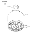
- FIG. 10 is a perspective view of a lighting unit according to an embodiment.
- FIG. 11 is a disassembled perspective view of a backlight unit according to an embodiment.
- a layer or film
- it can be directly on another layer or substrate, or intervening layers may also be present.
- intervening layers may also be present.
- a layer when a layer is referred to as being 'under' another layer, it can be directly under the other layer, and one or more intervening layers may also be present.
- a layer when referred to as being 'between' two layers, it can be the only layer between the two layers, or one or more intervening layers may also be present.
- FIG. 1 is a cross-sectional view of a light emitting device 100 according to an embodiment.
- the light emitting device (LED) 100 may include: a substrate 105, a first conductive type semiconductor layer 112 over the substrate 105, an active layer 114, and a second conductive type semiconductor layer 116.
- the first conductive type semiconductor layer 112, the active layer 114, and the second conductive type semiconductor layer 116 constitute a light emitting structure 110.
- a portion of the first conductive type semiconductor layer 112 is exposed.
- the LED 100 may also include a first region 121 having a first concentration and formed at a region of the second conductive type semiconductor layer 116, a second region 122 having a second concentration and formed at another region of the second conductive type semiconductor layer 116, a second electrode 146 over the second conductive semiconductor layer 116, and a first electrode 142 over an exposed region of the first conductive type semiconductor layer 112.
- the first region 121 having the first concentration and the second region 122 having the second concentration may be called ion implantation regions.
- the first concentration of the first region 121 may be lower than the second concentration of the second region 122.
- the first region 121 having the first concentration may be doped at an ion concentration of about 10 17 atom/cm 3 or less, but the present disclosure is not limited thereto.
- the first region 121 having the first concentration may be a shottkey contact region.
- the second concentration of the second region 122 may be higher than an ion concentration of the second conductive type semiconductor layer 116.
- the second region 122 having the second concentration may be doped at an ion concentration of 10 18 -10 19 atom/cm 3 or more, but the present disclosure is not limited thereto.
- the second region 122 having the second concentration may be an ohmic contact region.
- the second region 122 having the second concentration may be formed between the second electrode 146 and the mesa edge region, but the present disclosure is not limited thereto.
- the mesa edge region may include an opening region exposing at least a part of the etched first conductive semiconductor, but the present disclosure is not limited thereto.
- the first region 121 having the first concentration may be formed below the second electrode 146. At least one part of the first region 121 having the first concentration may be vertically overlapped with the second electrode 146.
- the LED 100 may include a transparent electrode 130 over the second conductive type semiconductor layer 116.
- FIGs. 2 and 3 are schematic views for describing shottkey contact and ohmic contact in an LED according to an embodiment.
- FIG. 2 shows that a shottkey contact is formed due to a low concentration doping of a p-type impurity
- FIG. 3 shows that as a doping concentration of a p-type impurity increases, a depletion width is decreased, and thus an ohmic contact is formed by a tunneling current mechanism.
- the second conductive type region 122 having the second concentration (high concentration) may be formed at a portion of the second conductive type semiconductor layer 116 doped at a low concentration through a diffusion or ion implantation.
- a region of the second conductive type semiconductor layer 116 below the second electrode 146 is doped at a low concentration, and a remaining region of the second conductive type semiconductor layer 116 other than the region of the second conductive type semiconductor layer 116 below the second electrode 146 is doped at a high concentration.
- the first region 121 having the second conductive type and lightly doped at the first concentration becomes a region for a shottkey contact
- the second region 122 having the second conductive region and heavily doped at the second concentration becomes a region for an ohmic contact.
- the first region of the for the shottkey contact acts as a current blocking layer (CBL)
- absorption of light in the second electrode 146 for example, p-metal can be decreased and light amount can be increased due to current spreading.
- absorption of light in the second electrode 146 can be decreased and light extracting efficiency can be enhanced through current spreading.
- An LED may be broken due to ESD under backward bias. Under the backward bias, a strong electric field is induced in an active region of the LED by charged particles.
- the second region 122 having the second concentration may be formed in the second conductive type semiconductor layer 116 around the mesa edge to induce an electric field.
- the second region 122 having the second concentration is a region having a higher concentration than the doping concentration of the second conductive type semiconductor layer 116, and may be formed by ion implantation or diffusion.
- the strong electric field generated in the mesa edge region may be induced into the second region 122 having the second concentration or may be suppressed to decrease the avalanche breakdown, so that the breakdown voltage may be increased and the leakage current may be decreased.
- the current spreading of the LED can be enhanced to induce an increase of light amount.
- the LED may be formed of a III-V compound semiconductor such as GaN, GaAs, GaAsP, GaP, or the like, but the present disclosure is not limited thereto.
- III-V compound semiconductor such as GaN, GaAs, GaAsP, GaP, or the like, but the present disclosure is not limited thereto.
- the sequence of processes to be described below is not limited to the following description, but may be modified.
- a substrate 105 is prepared.
- the substrate 105 may be at least one of sapphire (Al 2 O 3 ), SiC, Si, GaAs, GaN, ZnO, Si, GaP, InP, Ge and Ga 2 0 3 substrates. While an irregular structure may be formed at an upper surface of the substrate 105, the present disclosure is not limited thereto.
- a wet etching may be performed with respect to the substrate 105 to remove an impurity of a surface of the substrate 105.
- a light emitting structure 110 including a first conductive type semiconductor layer 112, an active layer 114 and a second conductive type semiconductor layer 116 may be formed over the substrate 105.
- the light emitting structure 110 may be formed by using, for example, a metal organic chemical vapor deposition (MOCVD), a chemical vapor deposition (CVD), a plasma-enhanced chemical vapor deposition (PECVD), a molecular beam epitaxy (MBE), a hydride vapor phase epitaxy (HVPE), or the like, but the present disclosure is not limited thereto.
- MOCVD metal organic chemical vapor deposition
- CVD chemical vapor deposition
- PECVD plasma-enhanced chemical vapor deposition
- MBE molecular beam epitaxy
- HVPE hydride vapor phase epitaxy
- a buffer layer (not shown) may be formed over the substrate 105.
- the buffer layer may buffer a lattice mismatch between the materials constituting the light emitting structure 110 and the substrate 105, and the buffer layer may be formed of a III-V compound semiconductor, for example, at least one of GaN, InN, A1N, InGaN, AlGaN, lnAlGaN, and AlInN.
- An undoped semiconductor layer (not shown) may be formed over the buffer layer, but the present disclosure is not limited thereto.
- the first conductive type semiconductor layer 112 may be implemented by a III-V compound semiconductor doped with a first conductive type dopant.
- the first conductive type dopant is an N-type dopant and may include Si, Ge, Sn, Se, and/or Te as the N-type dopant, but the present disclosure is not limited thereto.
- the first conductive type semiconductor layer 112 may include a semiconductor material having a compositional formula of In x Al y Ga 1 - x - y N (0 ⁇ x ⁇ 1, 0 ⁇ y ⁇ 1, 0 ⁇ x+y ⁇ 1).
- the first conductive type semiconductor layer 112 may be formed of at least one of GaN, InN, A1N, InGaN, AlGaN, InAlGaN, AlInN, AlGaAs, InGaAs, AlInGaAs, GaP, AlGaP, InGaP, AlInGaP, and InP.
- the first conductive type semiconductor layer 112 may be an N-type GaN layer, which is formed by using a chemical vapor deposition (CVD), a molecular beam epitaxy (MBE), a sputtering, a hydride vapor phase epitaxy (HVPE), or the like. Also, the first conductive type semiconductor layer 112 may be formed by injecting trimethyl gallium (TMGa) gas, ammonia (NH3) gas, nitrogen (N2) gas, and silane (SiH 4 ) gas including an n-type impurity such as silicon (Si).
- TMGa trimethyl gallium
- NH3 ammonia
- N2 nitrogen
- SiH 4 silane
- the active layer 114 may be formed in at least one of a single quantum well structure, a multi quantum well (MQW) structure, a quantum-wire structure, and a quantum dot structure.
- the active layer 114 may be formed in the MQW structure by injecting trimethyl gallium (TMGa) gas, ammonia (NH 3 ) gas, nitrogen (N 2 ) gas, and trimethyl indium (TMIn) gas, but the present disclosure is not limited thereto.
- TMGa trimethyl gallium
- NH 3 ammonia
- N 2 nitrogen
- TMIn trimethyl indium
- Well layer/barrier layer of the active layer 114 may be formed in at least one pair structure of InGaN/GaN, InGaN/InGaN, AlGaN/GaN, InAlGaN/GaN, GaAs/AlGaAs(InGaAs), GaP/AlGaP(InGaP), but the present disclosure is not limited thereto.
- the well layer may be formed of a material having a band gap lower than a band gap of the barrier layer.
- a conductive clad layer may be formed over or/and below the active layer 114.
- the conductive clad layer may be formed of an AlGaN-based semiconductor, and may have a band gap higher than the active layer 114.
- the second conductive type semiconductor layer 116 may include a III-V compound semiconductor, for example, semiconductor material having a compositional formula of In x Al y Ga 1 - x - y N (0 ⁇ x ⁇ 1, 0 ⁇ y ⁇ 1, 0 ⁇ x+y ⁇ 1).
- the second conductive type semiconductor layer 116 may be formed of at least one of GaN, InN, AlN, InGaN, AlGaN, lnAlGaN, AlInN, AlGaAs, InGaAs, AlInGaAs, GaP, AlGaP, InGaP, AlInGaP, and InP.
- the second conductive type dopant may include Mg, Zn, Ca, Sr, Ba, or the like as a P-type dopant.
- the second conductive type semiconductor layer 116 may be formed in a single- or multi-layer structure, but the present disclosure is not limited thereto.
- the second conductive type semiconductor layer 116 may be a P-type GaN layer, which is formed by injecting trimethyl gallium (TMGa) gas, ammonia (NH 3 ) gas, nitrogen (N 2 ) gas, and biscetyl cyclo pentadienyl magnesium ((EtCp 2 Mg) ⁇ Mg(C 2 H 5 C 5 H 4 ) 2 ⁇ ) including a P-type impurity such as Mg into a chamber, but the present disclosure is not limited thereto.
- TMGa trimethyl gallium
- NH 3 ammonia
- N 2 nitrogen
- EtCp 2 Mg biscetyl cyclo pentadienyl magnesium
- the first conductive type semiconductor layer 112 may be implemented by an N-type semiconductor layer and the second conductive type semiconductor layer 116 may be implemented by a P-type semiconductor layer, but the present disclosure is not limited thereto.
- a semiconductor layer having an opposite conductive type to the second conductive type for example, an N-type semiconductor layer (not shown) may be formed over the second semiconductor layer 116.
- the light emitting structure 110 may be implemented in at least one of an N-P junction structure, a P-N junction structure, an N-P-N junction structure, and a P-N-P junction structure.
- the light emitting structure 110 may be mesa-etched to expose a portion of the first conductive type semiconductor layer 112. For example, by sequentially etching the second conductive type semiconductor layer 116, the active layer 114, and an upper portion of the first conductive type semiconductor layer 112 at a region where the first electrode 142 is being formed, using a mask having a pattern (not shown), an upper surface of the first conductive type semiconductor layer 112 may be exposed.
- a first region 121 having a first concentration and a second region 122 having a second concentration may be formed in the second conductive type semiconductor layer 116.
- the first region 121 having the first concentration and the second region 122 having the second concentration may be formed by separate processes.
- the first concentration of the first region 121 may be lower than the second concentration of the second region 122.
- the first region 121 having the first concentration may be doped at an ion concentration of about 10 17 atom/cm 3 or less, but the present disclosure is not limited thereto.
- the first region 121 having the first concentration may be formed by an ion implantation or diffusion.
- the first region 121 may be a shottkey contact region.
- the first region 121 having the first concentration may be formed below the second electrode 146 to be formed later.
- the second concentration of the second region 122 may be higher than an ion concentration of the second conductive type semiconductor layer 116.
- the second region 122 having the second concentration may be doped at an ion concentration of 10 18 -10 19 atom/cm 3 or more, but the present disclosure is not limited thereto.
- the second region 122 having the second concentration may be an ohmic contact region.
- the second region 122 having the second concentration may be formed so as not to contact the mesa edge region, but the present disclosure is not limited thereto.
- the second region 122 having the second concentration may be formed between the second electrode and the mesa edge region, but the present disclosure is not limited thereto.
- the second region 122 having the second concentration is a region having a higher concentration than a doping concentration of the second conductive type semiconductor layer 116, and may be formed by an ion implantation or diffusion.
- the first region 121 having the second conductive type and lightly doped at the first concentration becomes a region for a shottkey contact
- the second region 122 having the second conductive region and heavily doped at the second concentration becomes a region for an ohmic contact
- absorption of light in the second electrode 146 can be decreased and light extracting efficiency can be enhanced through current spreading.
- the second region 122 having the second concentration has a structure for increasing the breakdown voltage, and may be formed in the second conductive type semiconductor layer 116 around the mesa edge to induce an electric field.
- the strong electric field generated in the mesa edge region may be induced into the second region 122 having the second concentration or may be suppressed to decrease the avalanche breakdown, so that the breakdown voltage may be increased and the leakage current may be decreased.
- a transparent electrode 130 may be formed over the second conductive type semiconductor layer 116 in which the second conductive ion implantation region 120 is formed.
- the transparent electrode 130 may be formed by multi-stacking a single metal layer, a metal alloy layer, and/or a metal oxide layer.
- the ohmic layer may be formed including at least one of indium tin oxide (ITO), indium zinc oxide (IZO), indium zinc tin oxide (IZTO), indium aluminum zinc oxide (IAZO), indium gallium zinc oxide (IGZO), indium gallium tin oxide (IGTO), aluminum zinc oxide (AZO), antimony tin oxide (ATO), gallium zinc oxide (GZO), IZO Nitride (IZON), Al-Ga ZnO (AGZO), In-Ga ZnO (IGZO), ZnO, IrOx, RuOx, NiO, RuOx/ITO, Ni/IrOx/Au, Ni/IrOx/Au/ITO, Ag, Ni, Cr, Ti, Al, Rh, Pd, Ir, Ru, Mg, Zn, Pt, Au, and Hf, but the present disclosure is not limited thereto.
- ITO indium tin oxide
- IZO indium zinc oxide
- IZTO indium aluminum
- a first electrode 142 may be formed over the exposed first conductive type semiconductor layer 112, and the second electrode 146 may be formed over the transparent electrode 130.
- the first and second electrodes 142 and 146 may be formed of at least one of titanium (Ti), chromium (Cr), nickel (Ni), aluminum (Al), platinum (Pt), gold (Au), and tungsten (W), but the present disclosure is not limited thereto.
- efficient current flow can be controlled to thus increase light extracting efficiency.
- the reliability of the LED can be enhanced by current spreading.
- an ESD damage of the LED can be prevented without loss followed by absorption of light.
- FIG. 9 is a cross-sectional view of a light emitting device package 200 according to an embodiment.
- the light emitting device package 200 includes a package body 205, third and fourth electrode layers 213 and 214 mounted over the package body 205, an LED 100 mounted over the package body 205 and electrically connected to the third and fourth electrode layers 213 and 214, and a molding member 240 enclosing the LED 100.
- the package body 205 may be formed including a silicon material, a synthetic resin material, or a metal material, and may have an inclination surface around the LED 100.
- the third electrode layer 213 and the fourth electrode layer 214 are electrically separated, and function to supply power to the LED 100. Also, the third and fourth electrode layers 213 and 214 may reflect light generated from the LED 100 to thus increase light efficiency, and may emit heat generated from the LED 100.
- the LED 100 may be a vertical type LED shown in FIG. 1 , but the present disclosure is not limited thereof.
- the LED 100 may be mounted over the package body 205 or over the third electrode layer 213 or the fourth electrode layer 214.
- the LED 100 may be electrically connected to the third electrode layer 213 and/or the fourth electrode layer 214 by using any one of a wire bonding method, a flip chip method, and a die bonding method. While the current embodiment exemplarily shows that the LED 100 is electrically connected to the third electrode layer 213 and the fourth electrode layer 214 through a wire 230, the present disclosure is not limited thereto.
- the molding member 240 may enclose and protect the LED 100. Also, a fluorescent material may be included in the molding member 240 to change the wavelength of light emitted from the LED 100.
- the light emitting device package may include a plurality of optical members, such as a light guide panel, a prism sheet, a diffusion sheet, a fluorescent sheet, and the like, which are arranged on a path of light emitted from the light emitting device package.
- the light emitting device package, substrate and optical members may function as a backlight unit or lighting unit, and a lighting system may include, for example, a backlight unit, a lighting unit, an indicator unit, a lamp, a streetlamp, etc.
- FIG. 10 is a perspective view of a lighting unit 1100 according to an embodiment.
- the lighting unit 110 shown in FIG. 10 is an example of lighting systems, and the present disclosure is not limited thereto.
- the lighting unit 1100 may include a case body 1110, a light emitting module part 1130 equipped in the case body 1110, and a connection terminal 1120 equipped in the case body 1110 and supplied with an electric power from an external power supply.
- the case body 110 may be preferably formed of a material having good heat shielding characteristics, for example, a metal material or a resin material.
- the light emitting module part 1130 may include a substrate 1132, and at least one light emitting device package 200 mounted on the substrate 1132.
- the substrate 1132 may be an insulator substrate on which a circuit pattern is printed, and may include, for example, a general printed circuit board (PCB), a metal core PCB, a flexible PCB, a ceramic PCB, etc.
- PCB general printed circuit board
- metal core PCB metal core PCB
- flexible PCB flexible PCB
- ceramic PCB ceramic PCB
- the substrate 1132 may be formed of a material to efficiently reflect light, and a surface thereof may be formed in a color capable of efficiently reflecting light, for example, white color, or silver color.
- the at least one light emitting device packages 200 may be mounted on the substrate 1132.
- Each of the light emitting device packages 200 may include at least one light emitting diode (LED) 100.
- the light emitting diode 100 may include a color LED emitting red, green, blue or white light, and a UV LED emitting ultraviolet (UV).
- the light emitting module part 1130 may have a combination of several LEDs so as to obtain desired color and luminance.
- the light emitting module part 1130 may have a combination of a white LED, a red LED, and a green LED so as to obtain a high color rendering index (CRI).
- CRI color rendering index
- connection terminal 1120 may be electrically connected to the light emitting module part 1130 to supply power. As shown in FIG. 10 , the connection terminal 1120 may be screwed and coupled to an external power in a socket type, but the present disclosure is not limited thereto. For example, the connection terminal 1120 may be made in a pin type and inserted into an external power, or may be connected to the external power through a power line.
- FIG. 11 is a disassembled perspective view of a backlight unit 1200 according to an embodiment.
- the backlight unit 1200 shown in FIG. 11 is an example of lighting systems, and the present disclosure is not limited thereto.
- the backlight unit 1200 may include a light guide panel 1210, a light emitting module part 1240 supplying light to the light guide panel 1210, a reflective member 1220 below the light guide panel 1210, and a bottom cover 1230 receiving the light guide panel 1210, the light emitting module part 1240, and the reflective member 1220, but the present disclosure is not limited thereto.
- the light guide panel 1210 functions to transform linear light to planar light by diffusing the linear light.
- the light guide panel may include one of acryl-series resin such as polymethyl metaacrylate (PMMA), polyethylene terephthlate (PET), poly carbonate (PC), COC, and polyethylene naphthalate resin.
- the light emitting module part 1240 provides light to at least a side surface of the light guide panel 1210, and finally acts as a light source of a display device in which the backlight unit is equipped.
- the light emitting module part 1240 may contact the light guide panel 1210, but the present disclosure is not limited thereto.
- the light emitting module part 1240 includes a substrate 1242, and a plurality of light emitting device packages 200 mounted on the substrate 1242.
- the substrate 1242 may contact the light guide panel 1210, but the present disclosure is not limited thereto.
- the substrate 1242 may be a PCB including a circuit pattern (not shown).
- the substrate 1242 may include a metal core PCB (MCPCB), a flexible PCB (FPCB), etc. as well as the general PCB, but the present disclosure is not limited thereto.
- MCPCB metal core PCB
- FPCB flexible PCB
- the plurality of light emitting device packages 200 may be mounted over the substrate 1242 such that light emitting surfaces of the plurality of light emitting device packages 200 are spaced apart by a predetermined distance from the light guide panel 1210.
- the reflective member 1220 may be provided below the light guide panel 1210.
- the reflective member 1220 reflects light incident from a bottom surface of the light guide panel to allow the reflected light to be directed toward an upper direction, thereby capable of enhancing brightness of the backlight unit.
- the reflective member 1220 may be formed of, for example, PET, PC, PVC resin, or the like, but the present disclosure is not limited thereto.
- the bottom cover 1230 may receive the light guide panel 1210, the light emitting module part 1240, the reflective member 1220, and the like.
- the bottom cover 1230 may be formed in a box shape a top surface of which is opened, but the present disclosure is not limited thereto.
- the bottom cover 1230 may be formed of a metal material or resin material, and may be manufactured by using a process such as a press molding or an injection molding.
- the lighting system according to the embodiment includes the light emitting device package according to the embodiment, so that the reliability can be enhanced.
- any reference in this specification to 'one embodiment,' 'an embodiment,' , example embodiment,' etc. means that a particular feature, structure, or characteristic described in connection with the embodiment is included in at least one embodiment of the invention.
- the appearances of such phrases in various places in the specification are not necessarily all referring to the same embodiment.
Landscapes
- Engineering & Computer Science (AREA)
- Power Engineering (AREA)
- Computer Hardware Design (AREA)
- Microelectronics & Electronic Packaging (AREA)
- Manufacturing & Machinery (AREA)
- Physics & Mathematics (AREA)
- Condensed Matter Physics & Semiconductors (AREA)
- General Physics & Mathematics (AREA)
- Led Devices (AREA)
- Non-Portable Lighting Devices Or Systems Thereof (AREA)
- Led Device Packages (AREA)
Abstract
Description
- Embodiments relate to a light emitting device, a light emitting device package, and a lighting system.
- A light emitting device (LED) may be implemented by a p-n junction diode, which has the characteristic converting an electrical energy to a light energy, and may be formed by combining a Group III element and a Group V element of the periodic table. The LED may implement various colors by adjusting the composition ratio of a compound semiconductor.
- Meanwhile, according to a related art, the lifetime and reliability may be lowered due to current spreading.
- Also, according to a related art, in an electrostatic discharge, current flows in a reverse direction, so that an active layer that is a light emitting region may be damaged. To solve the foregoing damage problem, a Zener diode may be equipped in an LED package, which may cause absorption of light.
- Embodiments provide a light emitting device, a light emitting device package, and a lighting system that can enhance light extraction efficiency as well as current spreading efficiency.
- Embodiments also provide a light emitting device, a light emitting device package, and a lighting system that can prevent damage due to the electrostatic discharge without loss according to absorption of light and can enhance light extraction efficiency as well as current spreading efficiency.
- In one embodiment, a light emitting device comprises: a substrate; a light emitting structure over the substrate, the light emitting structure including a first conductive type semiconductor layer, a second conductive type semiconductor layer, and an active layer between the first conductive type semiconductor layer and the second conductive type semiconductor layer, wherein the first conductive type semiconductor layer is partially exposed; a first region having a first concentration and provided at a region of the second conductive type semiconductor layer; a second region having a second concentration and provided at another region of the second conductive type semiconductor layer; and a second electrode over the second conductive type semiconductor layer.
- In another embodiment, a light emitting device package comprises: a package body; an electrode layer provided in the package body; and the above light emitting device electrically connected to the electrode layer.
- In a further embodiment, a lighting system comprises a light emitting module including a substrate, and a light emitting device package mounted over the substrate, wherein the light emitting device package comprises: a package body; an electrode layer provided in the package body; and the above light emitting device electrically connected to the electrode layer.
-
FIG. 1 is a cross-sectional view of a light emitting device according to an embodiment. -
FIGs. 2 and3 are schematic views for describing shottkey contact and ohmic contact according to an embodiment. -
FIGs. 4 and5 are schematic views for describing induction of an electric field according to an embodiment. -
FIGs. 6 through 8 are cross-sectional views illustrating a method for manufacturing a light emitting device according to a second embodiment. -
FIG. 9 is a cross-sectional view of a light emitting device package according to an embodiment. -
FIG. 10 is a perspective view of a lighting unit according to an embodiment. -
FIG. 11 is a disassembled perspective view of a backlight unit according to an embodiment. - Hereinafter, a light emitting device, a light emitting device package, and a lighting system according to the embodiments of the present disclosure will be described with reference to the accompanying drawings.
- In the description of embodiments, it will be understood that when a layer (or film) is referred to as being 'on' another layer or substrate, it can be directly on another layer or substrate, or intervening layers may also be present. Further, it will be understood that when a layer is referred to as being 'under' another layer, it can be directly under the other layer, and one or more intervening layers may also be present. In addition, it will also be understood that when a layer is referred to as being 'between' two layers, it can be the only layer between the two layers, or one or more intervening layers may also be present.
- (Embodiment)
-
FIG. 1 is a cross-sectional view of alight emitting device 100 according to an embodiment. - The light emitting device (LED) 100 according to an embodiment may include: a
substrate 105, a first conductivetype semiconductor layer 112 over thesubstrate 105, anactive layer 114, and a second conductivetype semiconductor layer 116. The first conductivetype semiconductor layer 112, theactive layer 114, and the second conductivetype semiconductor layer 116 constitute alight emitting structure 110. In thelight emitting structure 110, a portion of the first conductivetype semiconductor layer 112 is exposed. TheLED 100 may also include afirst region 121 having a first concentration and formed at a region of the second conductivetype semiconductor layer 116, asecond region 122 having a second concentration and formed at another region of the second conductivetype semiconductor layer 116, asecond electrode 146 over the secondconductive semiconductor layer 116, and afirst electrode 142 over an exposed region of the first conductivetype semiconductor layer 112. - The
first region 121 having the first concentration and thesecond region 122 having the second concentration may be called ion implantation regions. - The first concentration of the
first region 121 may be lower than the second concentration of thesecond region 122. For example, thefirst region 121 having the first concentration may be doped at an ion concentration of about 1017 atom/cm3 or less, but the present disclosure is not limited thereto. - Thus, the
first region 121 having the first concentration may be a shottkey contact region. - The second concentration of the
second region 122 may be higher than an ion concentration of the second conductivetype semiconductor layer 116. For example, thesecond region 122 having the second concentration may be doped at an ion concentration of 1018-1019 atom/cm3 or more, but the present disclosure is not limited thereto. - Thus, the
second region 122 having the second concentration may be an ohmic contact region. - The
second region 122 having the second concentration may be formed between thesecond electrode 146 and the mesa edge region, but the present disclosure is not limited thereto. The mesa edge region may include an opening region exposing at least a part of the etched first conductive semiconductor, but the present disclosure is not limited thereto.Thefirst region 121 having the first concentration may be formed below thesecond electrode 146. At least one part of thefirst region 121 having the first concentration may be vertically overlapped with thesecond electrode 146. - In the embodiment, The
LED 100 may include atransparent electrode 130 over the second conductivetype semiconductor layer 116. -
FIGs. 2 and3 are schematic views for describing shottkey contact and ohmic contact in an LED according to an embodiment. - Concretely,
FIG. 2 shows that a shottkey contact is formed due to a low concentration doping of a p-type impurity, andFIG. 3 shows that as a doping concentration of a p-type impurity increases, a depletion width is decreased, and thus an ohmic contact is formed by a tunneling current mechanism. - In the embodiment, as a structure to enhance the current spreading, the second
conductive type region 122 having the second concentration (high concentration) may be formed at a portion of the second conductivetype semiconductor layer 116 doped at a low concentration through a diffusion or ion implantation. - For example, a region of the second conductive
type semiconductor layer 116 below thesecond electrode 146 is doped at a low concentration, and a remaining region of the second conductivetype semiconductor layer 116 other than the region of the second conductivetype semiconductor layer 116 below thesecond electrode 146 is doped at a high concentration. - By doing so, the
first region 121 having the second conductive type and lightly doped at the first concentration becomes a region for a shottkey contact, and thesecond region 122 having the second conductive region and heavily doped at the second concentration becomes a region for an ohmic contact. - According to the embodiment, since the first region of the for the shottkey contact acts as a current blocking layer (CBL), absorption of light in the
second electrode 146, for example, p-metal can be decreased and light amount can be increased due to current spreading. - Therefore, according to the embodiment, absorption of light in the
second electrode 146 can be decreased and light extracting efficiency can be enhanced through current spreading. - Hereinafter, a concept for an electric field induction will be described with reference to
FIGs. 4 and5 . - An LED may be broken due to ESD under backward bias. Under the backward bias, a strong electric field is induced in an active region of the LED by charged particles.
- During ESD, carriers (electron & hole) are accelerated and collided with atoms to generate another carrier, and the generated carriers generate a lot of carriers. This phenomenon is called avalanche breakdown. If a strong electric field is induced by charged particles and thus a static electricity in excess of a limit that the semiconductor can endure is applied, the LED may be broken due to avalanche breakdown.
- In the embodiment, as a structure to increase a breakdown voltage, the
second region 122 having the second concentration may be formed in the second conductivetype semiconductor layer 116 around the mesa edge to induce an electric field. - The
second region 122 having the second concentration is a region having a higher concentration than the doping concentration of the second conductivetype semiconductor layer 116, and may be formed by ion implantation or diffusion. - According to the embodiment, as shown in
FIGs. 4 and5 and the following equation, the higher the doping concentration NA, ND is, the stronger the electric field induced in the depletion region by ionized charges is. -

-

- According to the embodiment, through the foregoing structure, the strong electric field generated in the mesa edge region may be induced into the
second region 122 having the second concentration or may be suppressed to decrease the avalanche breakdown, so that the breakdown voltage may be increased and the leakage current may be decreased. - Also, since the
second region 122 heavily doped at the second concentration is formed between thesecond electrode 146 and the mesa edge region, the current spreading of the LED can be enhanced to induce an increase of light amount. - Hereinafter, a method for manufacturing an LED according to an embodiment will be described with reference to
FIGs. 6 through 8 . In the embodiment, the LED may be formed of a III-V compound semiconductor such as GaN, GaAs, GaAsP, GaP, or the like, but the present disclosure is not limited thereto. The sequence of processes to be described below is not limited to the following description, but may be modified. - First, as shown in
FIG. 6 , asubstrate 105 is prepared. Thesubstrate 105 may be at least one of sapphire (Al2O3), SiC, Si, GaAs, GaN, ZnO, Si, GaP, InP, Ge and Ga203 substrates. While an irregular structure may be formed at an upper surface of thesubstrate 105, the present disclosure is not limited thereto. A wet etching may be performed with respect to thesubstrate 105 to remove an impurity of a surface of thesubstrate 105. - Thereafter, a
light emitting structure 110 including a first conductivetype semiconductor layer 112, anactive layer 114 and a second conductivetype semiconductor layer 116 may be formed over thesubstrate 105. - The
light emitting structure 110 may be formed by using, for example, a metal organic chemical vapor deposition (MOCVD), a chemical vapor deposition (CVD), a plasma-enhanced chemical vapor deposition (PECVD), a molecular beam epitaxy (MBE), a hydride vapor phase epitaxy (HVPE), or the like, but the present disclosure is not limited thereto. - A buffer layer (not shown) may be formed over the
substrate 105. The buffer layer may buffer a lattice mismatch between the materials constituting thelight emitting structure 110 and thesubstrate 105, and the buffer layer may be formed of a III-V compound semiconductor, for example, at least one of GaN, InN, A1N, InGaN, AlGaN, lnAlGaN, and AlInN. An undoped semiconductor layer (not shown) may be formed over the buffer layer, but the present disclosure is not limited thereto. - The first conductive
type semiconductor layer 112 may be implemented by a III-V compound semiconductor doped with a first conductive type dopant. In the case where the first conductivetype semiconductor layer 112 is an N-type semiconductor layer, the first conductive type dopant is an N-type dopant and may include Si, Ge, Sn, Se, and/or Te as the N-type dopant, but the present disclosure is not limited thereto. - The first conductive
type semiconductor layer 112 may include a semiconductor material having a compositional formula of InxAlyGa1-x-yN (0≤x≤1, 0≤y≤1, 0≤x+y≤1). - The first conductive
type semiconductor layer 112 may be formed of at least one of GaN, InN, A1N, InGaN, AlGaN, InAlGaN, AlInN, AlGaAs, InGaAs, AlInGaAs, GaP, AlGaP, InGaP, AlInGaP, and InP. - The first conductive
type semiconductor layer 112 may be an N-type GaN layer, which is formed by using a chemical vapor deposition (CVD), a molecular beam epitaxy (MBE), a sputtering, a hydride vapor phase epitaxy (HVPE), or the like. Also, the first conductivetype semiconductor layer 112 may be formed by injecting trimethyl gallium (TMGa) gas, ammonia (NH3) gas, nitrogen (N2) gas, and silane (SiH4) gas including an n-type impurity such as silicon (Si). - The
active layer 114 may be formed in at least one of a single quantum well structure, a multi quantum well (MQW) structure, a quantum-wire structure, and a quantum dot structure. For example, theactive layer 114 may be formed in the MQW structure by injecting trimethyl gallium (TMGa) gas, ammonia (NH3) gas, nitrogen (N2) gas, and trimethyl indium (TMIn) gas, but the present disclosure is not limited thereto. - Well layer/barrier layer of the
active layer 114 may be formed in at least one pair structure of InGaN/GaN, InGaN/InGaN, AlGaN/GaN, InAlGaN/GaN, GaAs/AlGaAs(InGaAs), GaP/AlGaP(InGaP), but the present disclosure is not limited thereto. The well layer may be formed of a material having a band gap lower than a band gap of the barrier layer. - A conductive clad layer may be formed over or/and below the
active layer 114. The conductive clad layer may be formed of an AlGaN-based semiconductor, and may have a band gap higher than theactive layer 114. - The second conductive
type semiconductor layer 116 may include a III-V compound semiconductor, for example, semiconductor material having a compositional formula of InxAlyGa1-x-yN (0≤x≤1, 0≤y≤1, 0≤x+y≤1). The second conductivetype semiconductor layer 116 may be formed of at least one of GaN, InN, AlN, InGaN, AlGaN, lnAlGaN, AlInN, AlGaAs, InGaAs, AlInGaAs, GaP, AlGaP, InGaP, AlInGaP, and InP. In the case where the second conductivetype semiconductor layer 116 is a P-type semiconductor layer, the second conductive type dopant may include Mg, Zn, Ca, Sr, Ba, or the like as a P-type dopant. The second conductivetype semiconductor layer 116 may be formed in a single- or multi-layer structure, but the present disclosure is not limited thereto. - The second conductive
type semiconductor layer 116 may be a P-type GaN layer, which is formed by injecting trimethyl gallium (TMGa) gas, ammonia (NH3) gas, nitrogen (N2) gas, and biscetyl cyclo pentadienyl magnesium ((EtCp2Mg){Mg(C2H5C5H4)2}) including a P-type impurity such as Mg into a chamber, but the present disclosure is not limited thereto. - In the embodiment, the first conductive
type semiconductor layer 112 may be implemented by an N-type semiconductor layer and the second conductivetype semiconductor layer 116 may be implemented by a P-type semiconductor layer, but the present disclosure is not limited thereto. Alternatively, a semiconductor layer having an opposite conductive type to the second conductive type, for example, an N-type semiconductor layer (not shown) may be formed over thesecond semiconductor layer 116. Accordingly, thelight emitting structure 110 may be implemented in at least one of an N-P junction structure, a P-N junction structure, an N-P-N junction structure, and a P-N-P junction structure. - Next, the
light emitting structure 110 may be mesa-etched to expose a portion of the first conductivetype semiconductor layer 112. For example, by sequentially etching the second conductivetype semiconductor layer 116, theactive layer 114, and an upper portion of the first conductivetype semiconductor layer 112 at a region where thefirst electrode 142 is being formed, using a mask having a pattern (not shown), an upper surface of the first conductivetype semiconductor layer 112 may be exposed. - Next, as shown in
FIG. 7 , afirst region 121 having a first concentration and asecond region 122 having a second concentration may be formed in the second conductivetype semiconductor layer 116. - The
first region 121 having the first concentration and thesecond region 122 having the second concentration may be formed by separate processes. - The first concentration of the
first region 121 may be lower than the second concentration of thesecond region 122. For example, thefirst region 121 having the first concentration may be doped at an ion concentration of about 1017 atom/cm3 or less, but the present disclosure is not limited thereto. - The
first region 121 having the first concentration may be formed by an ion implantation or diffusion. - Thus, the
first region 121 may be a shottkey contact region. - The
first region 121 having the first concentration may be formed below thesecond electrode 146 to be formed later. - The second concentration of the
second region 122 may be higher than an ion concentration of the second conductivetype semiconductor layer 116. For example, thesecond region 122 having the second concentration may be doped at an ion concentration of 1018 -1019 atom/cm3 or more, but the present disclosure is not limited thereto. - Thus, the
second region 122 having the second concentration may be an ohmic contact region. - The
second region 122 having the second concentration may be formed so as not to contact the mesa edge region, but the present disclosure is not limited thereto. - The
second region 122 having the second concentration may be formed between the second electrode and the mesa edge region, but the present disclosure is not limited thereto. - The
second region 122 having the second concentration is a region having a higher concentration than a doping concentration of the second conductivetype semiconductor layer 116, and may be formed by an ion implantation or diffusion. - In the embodiment, the
first region 121 having the second conductive type and lightly doped at the first concentration becomes a region for a shottkey contact, and thesecond region 122 having the second conductive region and heavily doped at the second concentration becomes a region for an ohmic contact. - Therefore, according to the embodiment, absorption of light in the
second electrode 146 can be decreased and light extracting efficiency can be enhanced through current spreading. - Also, in the embodiment, the
second region 122 having the second concentration has a structure for increasing the breakdown voltage, and may be formed in the second conductivetype semiconductor layer 116 around the mesa edge to induce an electric field. - According to the embodiment, through the foregoing structure, the strong electric field generated in the mesa edge region may be induced into the
second region 122 having the second concentration or may be suppressed to decrease the avalanche breakdown, so that the breakdown voltage may be increased and the leakage current may be decreased. - Next, as shown in
FIG. 8 , atransparent electrode 130 may be formed over the second conductivetype semiconductor layer 116 in which the second conductiveion implantation region 120 is formed. For example, thetransparent electrode 130 may be formed by multi-stacking a single metal layer, a metal alloy layer, and/or a metal oxide layer. For example, the ohmic layer may be formed including at least one of indium tin oxide (ITO), indium zinc oxide (IZO), indium zinc tin oxide (IZTO), indium aluminum zinc oxide (IAZO), indium gallium zinc oxide (IGZO), indium gallium tin oxide (IGTO), aluminum zinc oxide (AZO), antimony tin oxide (ATO), gallium zinc oxide (GZO), IZO Nitride (IZON), Al-Ga ZnO (AGZO), In-Ga ZnO (IGZO), ZnO, IrOx, RuOx, NiO, RuOx/ITO, Ni/IrOx/Au, Ni/IrOx/Au/ITO, Ag, Ni, Cr, Ti, Al, Rh, Pd, Ir, Ru, Mg, Zn, Pt, Au, and Hf, but the present disclosure is not limited thereto. - Next, a
first electrode 142 may be formed over the exposed first conductivetype semiconductor layer 112, and thesecond electrode 146 may be formed over thetransparent electrode 130. - The first and
second electrodes - By the LED and the method for manufacturing an LED according to the embodiments, efficient current flow can be controlled to thus increase light extracting efficiency.
- Also, according to the embodiments, the reliability of the LED can be enhanced by current spreading.
- Further, according to the embodiments, an ESD damage of the LED can be prevented without loss followed by absorption of light.
-
FIG. 9 is a cross-sectional view of a light emittingdevice package 200 according to an embodiment. - Referring to
FIG. 9 , the light emittingdevice package 200 according to the embodiment includes apackage body 205, third and fourth electrode layers 213 and 214 mounted over thepackage body 205, anLED 100 mounted over thepackage body 205 and electrically connected to the third and fourth electrode layers 213 and 214, and amolding member 240 enclosing theLED 100. - The
package body 205 may be formed including a silicon material, a synthetic resin material, or a metal material, and may have an inclination surface around theLED 100. - The
third electrode layer 213 and thefourth electrode layer 214 are electrically separated, and function to supply power to theLED 100. Also, the third and fourth electrode layers 213 and 214 may reflect light generated from theLED 100 to thus increase light efficiency, and may emit heat generated from theLED 100. - The
LED 100 may be a vertical type LED shown inFIG. 1 , but the present disclosure is not limited thereof. - The
LED 100 may be mounted over thepackage body 205 or over thethird electrode layer 213 or thefourth electrode layer 214. - The
LED 100 may be electrically connected to thethird electrode layer 213 and/or thefourth electrode layer 214 by using any one of a wire bonding method, a flip chip method, and a die bonding method. While the current embodiment exemplarily shows that theLED 100 is electrically connected to thethird electrode layer 213 and thefourth electrode layer 214 through awire 230, the present disclosure is not limited thereto. - The
molding member 240 may enclose and protect theLED 100. Also, a fluorescent material may be included in themolding member 240 to change the wavelength of light emitted from theLED 100. - The light emitting device package according to the embodiment may include a plurality of optical members, such as a light guide panel, a prism sheet, a diffusion sheet, a fluorescent sheet, and the like, which are arranged on a path of light emitted from the light emitting device package. The light emitting device package, substrate and optical members may function as a backlight unit or lighting unit, and a lighting system may include, for example, a backlight unit, a lighting unit, an indicator unit, a lamp, a streetlamp, etc.
-
FIG. 10 is a perspective view of alighting unit 1100 according to an embodiment. Thelighting unit 110 shown inFIG. 10 is an example of lighting systems, and the present disclosure is not limited thereto. - Referring to
FIG. 10 , thelighting unit 1100 may include acase body 1110, a light emittingmodule part 1130 equipped in thecase body 1110, and aconnection terminal 1120 equipped in thecase body 1110 and supplied with an electric power from an external power supply. - The
case body 110 may be preferably formed of a material having good heat shielding characteristics, for example, a metal material or a resin material. - The light emitting
module part 1130 may include asubstrate 1132, and at least one light emittingdevice package 200 mounted on thesubstrate 1132. - The
substrate 1132 may be an insulator substrate on which a circuit pattern is printed, and may include, for example, a general printed circuit board (PCB), a metal core PCB, a flexible PCB, a ceramic PCB, etc. - Also, the
substrate 1132 may be formed of a material to efficiently reflect light, and a surface thereof may be formed in a color capable of efficiently reflecting light, for example, white color, or silver color. - The at least one light emitting device packages 200 may be mounted on the
substrate 1132. Each of the light emitting device packages 200 may include at least one light emitting diode (LED) 100. Thelight emitting diode 100 may include a color LED emitting red, green, blue or white light, and a UV LED emitting ultraviolet (UV). - The light emitting
module part 1130 may have a combination of several LEDs so as to obtain desired color and luminance. For example, the light emittingmodule part 1130 may have a combination of a white LED, a red LED, and a green LED so as to obtain a high color rendering index (CRI). - The
connection terminal 1120 may be electrically connected to the light emittingmodule part 1130 to supply power. As shown inFIG. 10 , theconnection terminal 1120 may be screwed and coupled to an external power in a socket type, but the present disclosure is not limited thereto. For example, theconnection terminal 1120 may be made in a pin type and inserted into an external power, or may be connected to the external power through a power line. -
FIG. 11 is a disassembled perspective view of abacklight unit 1200 according to an embodiment. Thebacklight unit 1200 shown inFIG. 11 is an example of lighting systems, and the present disclosure is not limited thereto. - The
backlight unit 1200 according to the embodiment may include alight guide panel 1210, a light emittingmodule part 1240 supplying light to thelight guide panel 1210, areflective member 1220 below thelight guide panel 1210, and abottom cover 1230 receiving thelight guide panel 1210, the light emittingmodule part 1240, and thereflective member 1220, but the present disclosure is not limited thereto. - The
light guide panel 1210 functions to transform linear light to planar light by diffusing the linear light. For example, the light guide panel may include one of acryl-series resin such as polymethyl metaacrylate (PMMA), polyethylene terephthlate (PET), poly carbonate (PC), COC, and polyethylene naphthalate resin. - The light emitting
module part 1240 provides light to at least a side surface of thelight guide panel 1210, and finally acts as a light source of a display device in which the backlight unit is equipped. - The light emitting
module part 1240 may contact thelight guide panel 1210, but the present disclosure is not limited thereto. Concretely, the light emittingmodule part 1240 includes asubstrate 1242, and a plurality of light emitting device packages 200 mounted on thesubstrate 1242. Thesubstrate 1242 may contact thelight guide panel 1210, but the present disclosure is not limited thereto. - The
substrate 1242 may be a PCB including a circuit pattern (not shown). Thesubstrate 1242 may include a metal core PCB (MCPCB), a flexible PCB (FPCB), etc. as well as the general PCB, but the present disclosure is not limited thereto. - The plurality of light emitting device packages 200 may be mounted over the
substrate 1242 such that light emitting surfaces of the plurality of light emitting device packages 200 are spaced apart by a predetermined distance from thelight guide panel 1210. - The
reflective member 1220 may be provided below thelight guide panel 1210. Thereflective member 1220 reflects light incident from a bottom surface of the light guide panel to allow the reflected light to be directed toward an upper direction, thereby capable of enhancing brightness of the backlight unit. Thereflective member 1220 may be formed of, for example, PET, PC, PVC resin, or the like, but the present disclosure is not limited thereto. - The
bottom cover 1230 may receive thelight guide panel 1210, the light emittingmodule part 1240, thereflective member 1220, and the like. For this purpose, thebottom cover 1230 may be formed in a box shape a top surface of which is opened, but the present disclosure is not limited thereto. - The
bottom cover 1230 may be formed of a metal material or resin material, and may be manufactured by using a process such as a press molding or an injection molding. - As described above, the lighting system according to the embodiment includes the light emitting device package according to the embodiment, so that the reliability can be enhanced.
- Any reference in this specification to 'one embodiment,' 'an embodiment,' ,example embodiment,' etc., means that a particular feature, structure, or characteristic described in connection with the embodiment is included in at least one embodiment of the invention. The appearances of such phrases in various places in the specification are not necessarily all referring to the same embodiment. Further, when a particular feature, structure, or characteristic is described in connection with any embodiment, it is submitted that it is within the purview of one skilled in the art to effect such feature, structure, or characteristic in connection with other ones of the embodiments.
- Although embodiments have been described with reference to a number of illustrative embodiments thereof, it should be understood that numerous other modifications and embodiments can be devised by those skilled in the art that will fall within the spirit and scope of the principles of this disclosure. More particularly, various variations and modifications are possible in the component parts and/or arrangements of the subject combination arrangement within the scope of the disclosure, the drawings and the appended claims. In addition to variations and modifications in the component parts and/or arrangements, alternative uses will also be apparent to those skilled in the art.
Claims (14)
- A light emitting device comprising:a substrate;a light emitting structure over the substrate, the light emitting structure including a first conductive type semiconductor layer, a second conductive type semiconductor layer, and an active layer between the first conductive type semiconductor layer and the second conductive type semiconductor layer, wherein the first conductive type semiconductor layer is partially exposed;a first region having a first concentration and provided at a region of the second conductive type semiconductor layer;a second region having a second concentration and provided at another region of the second conductive type semiconductor layer; anda second electrode over the second conductive type semiconductor layer.
- The light emitting device of claim 1, comprising a first electrode over the exposed first conductive type semiconductor layer.
- The light emitting device of claim 1, wherein the first region having the first concentration and is a second conductive type ion implantation region.
- The light emitting device of claim 3, wherein the first region having the first concentration is formed at a concentration lower than an ion concentration of the second conductive type semiconductor layer.
- The light emitting device of claim 4, wherein the first region 121 having the first concentration is doped at an ion concentration of 1017 atom/cm3 or less.
- The light emitting device of claim 1, wherein the first region having the first concentration is a shottkey contact region.
- The light emitting device of claim 1, wherein the second region having the second concentration is a second conductive type ion implantation region.
- The light emitting device of claim 7, wherein the second region having the second concentration is formed at a concentration higher than an ion concentration of the second conductive type semiconductor layer.
- The light emitting device of claim 8, wherein the second concentration is doped at an ion concentration of 1018_1019 atom/cm3 or more.
- The light emitting device of claim 1, wherein the second region having the second concentration is an ohmic contact region.
- The light emitting device of claim 1, wherein the second region having the second concentration is formed between the second electrode and a mesa edge region.
- The light emitting device of claim 1, wherein at least one part of the first region having the first concentration is vertically overlapped with the second electrode.
- A light emitting device package comprising:a package body;an electrode layer provided in the package body; anda light emitting device accdoring to any one of claims 1 to 12 electrically connected to the electrode layer.
- A lighting system comprising a light emitting module including a substrate, and a light emitting device package mounted over the substrate,
wherein the light emitting device package comprises:a package body;an electrode layer provided in the package body; anda light emitting device of claim 13 electrically connected to the electrode layer.
Applications Claiming Priority (1)
| Application Number | Priority Date | Filing Date | Title |
|---|---|---|---|
| KR20090132733A KR100999787B1 (en) | 2009-12-29 | 2009-12-29 | Light emitting device, method for fabricating the same and light emitting device package |
Publications (3)
| Publication Number | Publication Date |
|---|---|
| EP2341557A2 true EP2341557A2 (en) | 2011-07-06 |
| EP2341557A3 EP2341557A3 (en) | 2014-01-08 |
| EP2341557B1 EP2341557B1 (en) | 2017-05-17 |
Family
ID=43512613
Family Applications (1)
| Application Number | Title | Priority Date | Filing Date |
|---|---|---|---|
| EP10196010.2A Not-in-force EP2341557B1 (en) | 2009-12-29 | 2010-12-20 | Light emitting diode, light emitting diode package and lighting system |
Country Status (6)
| Country | Link |
|---|---|
| US (2) | US20110156089A1 (en) |
| EP (1) | EP2341557B1 (en) |
| JP (1) | JP2011139066A (en) |
| KR (1) | KR100999787B1 (en) |
| CN (1) | CN102110752B (en) |
| TW (1) | TWI449216B (en) |
Cited By (1)
| Publication number | Priority date | Publication date | Assignee | Title |
|---|---|---|---|---|
| EP2827390A1 (en) | 2013-07-15 | 2015-01-21 | Commissariat A L'energie Atomique Et Aux Energies Alternatives | Emissive structure with lateral injection of carriers |
Families Citing this family (15)
| Publication number | Priority date | Publication date | Assignee | Title |
|---|---|---|---|---|
| KR101280221B1 (en) | 2011-05-13 | 2013-07-05 | (주)버티클 | Semiconductor devices and fabrication method thereof |
| TWI594461B (en) * | 2011-08-04 | 2017-08-01 | 國家中山科學研究院 | Fluorescent coating and a method for making the same |
| KR101219290B1 (en) | 2011-11-08 | 2013-01-21 | 순천대학교 산학협력단 | Method for fabricating light emitting diodes |
| KR101267437B1 (en) * | 2011-11-08 | 2013-05-31 | 순천대학교 산학협력단 | Light emitting diodes and method for fabricating the same |
| KR102029658B1 (en) * | 2013-01-31 | 2019-10-08 | 엘지이노텍 주식회사 | Light emitting device |
| KR102057719B1 (en) | 2013-04-29 | 2019-12-19 | 엘지이노텍 주식회사 | Light emitting device and lighting system |
| CN104134728B (en) * | 2013-05-03 | 2018-10-09 | 上海蓝光科技有限公司 | A kind of manufacturing method of light emitting diode |
| TWI505502B (en) * | 2013-08-16 | 2015-10-21 | Lextar Electronics Corp | Light-emitting diode and method for manufacturing thereof |
| JP2015056647A (en) * | 2013-09-13 | 2015-03-23 | 株式会社東芝 | Nitride semiconductor light-emitting device |
| US9673368B2 (en) * | 2015-05-11 | 2017-06-06 | Lg Innotek Co., Ltd. | Light emitting device having first and second electrodes on one side of a light emitting structure |
| KR102363038B1 (en) * | 2015-11-10 | 2022-02-15 | 쑤저우 레킨 세미컨덕터 컴퍼니 리미티드 | Light emitting device and method of fabricating the same |
| US11024773B2 (en) * | 2016-11-07 | 2021-06-01 | Goertek. Inc | Micro-LED with vertical structure, display device, electronics apparatus and manufacturing method |
| CN107358780B (en) * | 2017-07-30 | 2020-01-03 | 王旭兰 | Intelligent electric spark detection alarm system based on PN junction chip and preparation method thereof |
| EP3923351A4 (en) * | 2020-03-03 | 2023-01-04 | HCP Technology Co., Ltd. | Light-emitting diode and preparation method therefor |
| TWI833091B (en) * | 2021-07-12 | 2024-02-21 | 錼創顯示科技股份有限公司 | Micro light emitting diode chip |
Family Cites Families (19)
| Publication number | Priority date | Publication date | Assignee | Title |
|---|---|---|---|---|
| JPH088458A (en) * | 1994-06-22 | 1996-01-12 | Daido Steel Co Ltd | Surface type light emitting diode |
| JPH08153892A (en) * | 1994-09-30 | 1996-06-11 | Rohm Co Ltd | Semiconductor light emitting element and fabrication thereof |
| JPH08186287A (en) * | 1994-12-28 | 1996-07-16 | Rohm Co Ltd | Semiconductor light-emitting diode |
| JPH08250768A (en) * | 1995-03-13 | 1996-09-27 | Toyoda Gosei Co Ltd | Semiconductor optical element |
| JP3741528B2 (en) * | 1997-12-15 | 2006-02-01 | シャープ株式会社 | Method for manufacturing gallium nitride based semiconductor device |
| JP4382912B2 (en) | 1999-08-26 | 2009-12-16 | 昭和電工株式会社 | AlGaInP light emitting diode |
| US6420736B1 (en) * | 2000-07-26 | 2002-07-16 | Axt, Inc. | Window for gallium nitride light emitting diode |
| KR20030066957A (en) | 2002-02-06 | 2003-08-14 | 주식회사 엘지이아이 | Method for manufacturing a light emitting device made from Ⅲ-Ⅴgroup chemical compound semiconductor |
| KR20050035325A (en) | 2003-10-10 | 2005-04-18 | 삼성전기주식회사 | Nitride semiconductor light emitting device and method of manufacturing the same |
| KR20050093319A (en) * | 2004-03-18 | 2005-09-23 | 삼성전기주식회사 | Nitride-based semiconductor led having improved luminous efficiency and fabrication method thereof |
| JP2006156458A (en) * | 2004-11-25 | 2006-06-15 | Toshiba Corp | Semiconductor light emitting device and its manufacturing method |
| EP1928030B1 (en) * | 2005-09-20 | 2019-01-30 | Panasonic Intellectual Property Management Co., Ltd. | Led lighting fixture |
| KR100746783B1 (en) * | 2006-02-28 | 2007-08-06 | 엘지전자 주식회사 | Light emitting device package and method of fabricating the same |
| JP4967538B2 (en) * | 2006-08-30 | 2012-07-04 | 富士ゼロックス株式会社 | Surface light emitting device, image reading device and image writing device using surface light emitting device, and method for manufacturing surface light emitting device |
| TWI338380B (en) * | 2006-10-11 | 2011-03-01 | Chuan Yu Hung | Light emitting diode incorporating high refractive index material |
| KR100906209B1 (en) * | 2007-08-06 | 2009-07-07 | 경신공업 주식회사 | Terminal feeder |
| KR20090104454A (en) * | 2008-03-31 | 2009-10-06 | 삼성전기주식회사 | Nitride Light Emitting Device |
| WO2009134095A2 (en) * | 2008-04-30 | 2009-11-05 | 엘지이노텍주식회사 | Light-emitting element and a production method therefor |
| KR100952034B1 (en) * | 2008-05-08 | 2010-04-07 | 엘지이노텍 주식회사 | Light emitting device and method for fabricating the same |
-
2009
- 2009-12-29 KR KR20090132733A patent/KR100999787B1/en active IP Right Grant
-
2010
- 2010-12-20 TW TW99144698A patent/TWI449216B/en active
- 2010-12-20 EP EP10196010.2A patent/EP2341557B1/en not_active Not-in-force
- 2010-12-28 CN CN2010106226130A patent/CN102110752B/en not_active Expired - Fee Related
- 2010-12-28 US US12/980,213 patent/US20110156089A1/en not_active Abandoned
- 2010-12-28 JP JP2010291804A patent/JP2011139066A/en active Pending
-
2011
- 2011-12-19 US US13/330,207 patent/US8530926B2/en active Active
Non-Patent Citations (1)
| Title |
|---|
| None |
Cited By (2)
| Publication number | Priority date | Publication date | Assignee | Title |
|---|---|---|---|---|
| EP2827390A1 (en) | 2013-07-15 | 2015-01-21 | Commissariat A L'energie Atomique Et Aux Energies Alternatives | Emissive structure with lateral injection of carriers |
| US9905734B2 (en) | 2013-07-15 | 2018-02-27 | Commissariat A L'energie Atomique Et Aux Energies Alternatives | Emissive structure with lateral carrier injection |
Also Published As
| Publication number | Publication date |
|---|---|
| CN102110752A (en) | 2011-06-29 |
| KR100999787B1 (en) | 2010-12-08 |
| JP2011139066A (en) | 2011-07-14 |
| US8530926B2 (en) | 2013-09-10 |
| CN102110752B (en) | 2013-07-17 |
| TWI449216B (en) | 2014-08-11 |
| US20110156089A1 (en) | 2011-06-30 |
| TW201126762A (en) | 2011-08-01 |
| EP2341557A3 (en) | 2014-01-08 |
| EP2341557B1 (en) | 2017-05-17 |
| US20120091497A1 (en) | 2012-04-19 |
Similar Documents
| Publication | Publication Date | Title |
|---|---|---|
| EP2341557B1 (en) | Light emitting diode, light emitting diode package and lighting system | |
| EP2320483B1 (en) | Light emitting device, light emitting device package and lighting system | |
| EP2369646B1 (en) | Light emitting device, light emitting device package and lighting system | |
| EP2315273B1 (en) | Light emitting device and light emitting device package | |
| US9287460B2 (en) | Light emitting device, light emitting device package and lighting system including the same | |
| US8669586B2 (en) | Light emitting device, light emitting device package, and lighting system | |
| EP2482343A2 (en) | Light emitting diode | |
| US8362514B2 (en) | Vertical semiconductor light emitting device including a capacitor | |
| EP2544248A1 (en) | Light emitting device | |
| EP2246891B1 (en) | Light emitting device, light emitting device package, and lighting system including the same | |
| EP2296196B1 (en) | Light emitting device | |
| EP2405500B1 (en) | Semiconducting light emitting device with resonance condition between bottom reflector and active layer | |
| EP2383803A2 (en) | Light emitting device with a stepped transparent electrode | |
| EP2375450B1 (en) | Light emitting diode and LED package | |
| KR20120138275A (en) | Light emitting device | |
| EP2369647A2 (en) | Light emitting device, light emitting device package and lighting system | |
| KR20130007314A (en) | Light emitting device | |
| KR20110120080A (en) | Light emitting device, method for fabricating the same, light emitting device package and lighting system including the same | |
| KR20130006845A (en) | Light emitting device and method for fabricating the same |
Legal Events
| Date | Code | Title | Description |
|---|---|---|---|
| PUAI | Public reference made under article 153(3) epc to a published international application that has entered the european phase |
Free format text: ORIGINAL CODE: 0009012 |
|
| 17P | Request for examination filed |
Effective date: 20101220 |
|
| AK | Designated contracting states |
Kind code of ref document: A2 Designated state(s): AL AT BE BG CH CY CZ DE DK EE ES FI FR GB GR HR HU IE IS IT LI LT LU LV MC MK MT NL NO PL PT RO RS SE SI SK SM TR |
|
| AX | Request for extension of the european patent |
Extension state: BA ME |
|
| PUAL | Search report despatched |
Free format text: ORIGINAL CODE: 0009013 |
|
| AK | Designated contracting states |
Kind code of ref document: A3 Designated state(s): AL AT BE BG CH CY CZ DE DK EE ES FI FR GB GR HR HU IE IS IT LI LT LU LV MC MK MT NL NO PL PT RO RS SE SI SK SM TR |
|
| AX | Request for extension of the european patent |
Extension state: BA ME |
|
| RIC1 | Information provided on ipc code assigned before grant |
Ipc: H01L 33/32 20100101ALN20131129BHEP Ipc: H01L 33/02 20100101ALN20131129BHEP Ipc: H01L 33/40 20100101ALN20131129BHEP Ipc: H01L 33/00 20100101ALN20131129BHEP Ipc: H01L 27/15 20060101ALI20131129BHEP Ipc: H01L 33/14 20100101AFI20131129BHEP |
|
| RAP1 | Party data changed (applicant data changed or rights of an application transferred) |
Owner name: LG INNOTEK CO., LTD. |
|
| RBV | Designated contracting states (corrected) |
Designated state(s): AL AT BE BG CH CY CZ DE DK EE ES FI FR GB GR HR HU IE IS IT LI LT LU LV MC MK MT NL NO PL PT RO RS SE SI SK SM TR |
|
| 17Q | First examination report despatched |
Effective date: 20150723 |
|
| GRAP | Despatch of communication of intention to grant a patent |
Free format text: ORIGINAL CODE: EPIDOSNIGR1 |
|
| INTG | Intention to grant announced |
Effective date: 20161007 |
|
| RIN1 | Information on inventor provided before grant (corrected) |
Inventor name: HWANG, SUNG MIN |
|
| GRAJ | Information related to disapproval of communication of intention to grant by the applicant or resumption of examination proceedings by the epo deleted |
Free format text: ORIGINAL CODE: EPIDOSDIGR1 |
|
| STAA | Information on the status of an ep patent application or granted ep patent |
Free format text: STATUS: EXAMINATION IS IN PROGRESS |
|
| GRAP | Despatch of communication of intention to grant a patent |
Free format text: ORIGINAL CODE: EPIDOSNIGR1 |
|
| STAA | Information on the status of an ep patent application or granted ep patent |
Free format text: STATUS: GRANT OF PATENT IS INTENDED |
|
| INTG | Intention to grant announced |
Effective date: 20170215 |
|
| GRAS | Grant fee paid |
Free format text: ORIGINAL CODE: EPIDOSNIGR3 |
|
| GRAA | (expected) grant |
Free format text: ORIGINAL CODE: 0009210 |
|
| STAA | Information on the status of an ep patent application or granted ep patent |
Free format text: STATUS: THE PATENT HAS BEEN GRANTED |
|
| AK | Designated contracting states |
Kind code of ref document: B1 Designated state(s): AL AT BE BG CH CY CZ DE DK EE ES FI FR GB GR HR HU IE IS IT LI LT LU LV MC MK MT NL NO PL PT RO RS SE SI SK SM TR |
|
| RAP1 | Party data changed (applicant data changed or rights of an application transferred) |
Owner name: LG INNOTEK CO., LTD. |
|
| REG | Reference to a national code |
Ref country code: GB Ref legal event code: FG4D |
|
| REG | Reference to a national code |
Ref country code: CH Ref legal event code: EP |
|
| REG | Reference to a national code |
Ref country code: IE Ref legal event code: FG4D |
|
| REG | Reference to a national code |
Ref country code: AT Ref legal event code: REF Ref document number: 895182 Country of ref document: AT Kind code of ref document: T Effective date: 20170615 |
|
| REG | Reference to a national code |
Ref country code: DE Ref legal event code: R096 Ref document number: 602010042381 Country of ref document: DE |
|
| REG | Reference to a national code |
Ref country code: NL Ref legal event code: FP |
|
| REG | Reference to a national code |
Ref country code: LT Ref legal event code: MG4D |
|
| REG | Reference to a national code |
Ref country code: AT Ref legal event code: MK05 Ref document number: 895182 Country of ref document: AT Kind code of ref document: T Effective date: 20170517 |
|
| PG25 | Lapsed in a contracting state [announced via postgrant information from national office to epo] |
Ref country code: NO Free format text: LAPSE BECAUSE OF FAILURE TO SUBMIT A TRANSLATION OF THE DESCRIPTION OR TO PAY THE FEE WITHIN THE PRESCRIBED TIME-LIMIT Effective date: 20170817 Ref country code: LT Free format text: LAPSE BECAUSE OF FAILURE TO SUBMIT A TRANSLATION OF THE DESCRIPTION OR TO PAY THE FEE WITHIN THE PRESCRIBED TIME-LIMIT Effective date: 20170517 Ref country code: FI Free format text: LAPSE BECAUSE OF FAILURE TO SUBMIT A TRANSLATION OF THE DESCRIPTION OR TO PAY THE FEE WITHIN THE PRESCRIBED TIME-LIMIT Effective date: 20170517 Ref country code: GR Free format text: LAPSE BECAUSE OF FAILURE TO SUBMIT A TRANSLATION OF THE DESCRIPTION OR TO PAY THE FEE WITHIN THE PRESCRIBED TIME-LIMIT Effective date: 20170818 Ref country code: AT Free format text: LAPSE BECAUSE OF FAILURE TO SUBMIT A TRANSLATION OF THE DESCRIPTION OR TO PAY THE FEE WITHIN THE PRESCRIBED TIME-LIMIT Effective date: 20170517 Ref country code: HR Free format text: LAPSE BECAUSE OF FAILURE TO SUBMIT A TRANSLATION OF THE DESCRIPTION OR TO PAY THE FEE WITHIN THE PRESCRIBED TIME-LIMIT Effective date: 20170517 Ref country code: ES Free format text: LAPSE BECAUSE OF FAILURE TO SUBMIT A TRANSLATION OF THE DESCRIPTION OR TO PAY THE FEE WITHIN THE PRESCRIBED TIME-LIMIT Effective date: 20170517 |
|
| PG25 | Lapsed in a contracting state [announced via postgrant information from national office to epo] |
Ref country code: BG Free format text: LAPSE BECAUSE OF FAILURE TO SUBMIT A TRANSLATION OF THE DESCRIPTION OR TO PAY THE FEE WITHIN THE PRESCRIBED TIME-LIMIT Effective date: 20170817 Ref country code: IS Free format text: LAPSE BECAUSE OF FAILURE TO SUBMIT A TRANSLATION OF THE DESCRIPTION OR TO PAY THE FEE WITHIN THE PRESCRIBED TIME-LIMIT Effective date: 20170917 Ref country code: SE Free format text: LAPSE BECAUSE OF FAILURE TO SUBMIT A TRANSLATION OF THE DESCRIPTION OR TO PAY THE FEE WITHIN THE PRESCRIBED TIME-LIMIT Effective date: 20170517 Ref country code: RS Free format text: LAPSE BECAUSE OF FAILURE TO SUBMIT A TRANSLATION OF THE DESCRIPTION OR TO PAY THE FEE WITHIN THE PRESCRIBED TIME-LIMIT Effective date: 20170517 Ref country code: LV Free format text: LAPSE BECAUSE OF FAILURE TO SUBMIT A TRANSLATION OF THE DESCRIPTION OR TO PAY THE FEE WITHIN THE PRESCRIBED TIME-LIMIT Effective date: 20170517 Ref country code: PL Free format text: LAPSE BECAUSE OF FAILURE TO SUBMIT A TRANSLATION OF THE DESCRIPTION OR TO PAY THE FEE WITHIN THE PRESCRIBED TIME-LIMIT Effective date: 20170517 |
|
| PG25 | Lapsed in a contracting state [announced via postgrant information from national office to epo] |
Ref country code: RO Free format text: LAPSE BECAUSE OF FAILURE TO SUBMIT A TRANSLATION OF THE DESCRIPTION OR TO PAY THE FEE WITHIN THE PRESCRIBED TIME-LIMIT Effective date: 20170517 Ref country code: EE Free format text: LAPSE BECAUSE OF FAILURE TO SUBMIT A TRANSLATION OF THE DESCRIPTION OR TO PAY THE FEE WITHIN THE PRESCRIBED TIME-LIMIT Effective date: 20170517 Ref country code: CZ Free format text: LAPSE BECAUSE OF FAILURE TO SUBMIT A TRANSLATION OF THE DESCRIPTION OR TO PAY THE FEE WITHIN THE PRESCRIBED TIME-LIMIT Effective date: 20170517 Ref country code: SK Free format text: LAPSE BECAUSE OF FAILURE TO SUBMIT A TRANSLATION OF THE DESCRIPTION OR TO PAY THE FEE WITHIN THE PRESCRIBED TIME-LIMIT Effective date: 20170517 Ref country code: DK Free format text: LAPSE BECAUSE OF FAILURE TO SUBMIT A TRANSLATION OF THE DESCRIPTION OR TO PAY THE FEE WITHIN THE PRESCRIBED TIME-LIMIT Effective date: 20170517 |
|
| REG | Reference to a national code |
Ref country code: DE Ref legal event code: R097 Ref document number: 602010042381 Country of ref document: DE |
|
| PG25 | Lapsed in a contracting state [announced via postgrant information from national office to epo] |
Ref country code: SM Free format text: LAPSE BECAUSE OF FAILURE TO SUBMIT A TRANSLATION OF THE DESCRIPTION OR TO PAY THE FEE WITHIN THE PRESCRIBED TIME-LIMIT Effective date: 20170517 Ref country code: IT Free format text: LAPSE BECAUSE OF FAILURE TO SUBMIT A TRANSLATION OF THE DESCRIPTION OR TO PAY THE FEE WITHIN THE PRESCRIBED TIME-LIMIT Effective date: 20170517 |
|
| PLBE | No opposition filed within time limit |
Free format text: ORIGINAL CODE: 0009261 |
|
| STAA | Information on the status of an ep patent application or granted ep patent |
Free format text: STATUS: NO OPPOSITION FILED WITHIN TIME LIMIT |
|
| 26N | No opposition filed |
Effective date: 20180220 |
|
| PG25 | Lapsed in a contracting state [announced via postgrant information from national office to epo] |
Ref country code: SI Free format text: LAPSE BECAUSE OF FAILURE TO SUBMIT A TRANSLATION OF THE DESCRIPTION OR TO PAY THE FEE WITHIN THE PRESCRIBED TIME-LIMIT Effective date: 20170517 |
|
| REG | Reference to a national code |
Ref country code: CH Ref legal event code: PL |
|
| REG | Reference to a national code |
Ref country code: NL Ref legal event code: MM Effective date: 20180101 |
|
| GBPC | Gb: european patent ceased through non-payment of renewal fee |
Effective date: 20171220 |
|
| REG | Reference to a national code |
Ref country code: IE Ref legal event code: MM4A |
|
| PG25 | Lapsed in a contracting state [announced via postgrant information from national office to epo] |
Ref country code: NL Free format text: LAPSE BECAUSE OF NON-PAYMENT OF DUE FEES Effective date: 20180101 Ref country code: MT Free format text: LAPSE BECAUSE OF NON-PAYMENT OF DUE FEES Effective date: 20171220 Ref country code: LU Free format text: LAPSE BECAUSE OF NON-PAYMENT OF DUE FEES Effective date: 20171220 |
|
| REG | Reference to a national code |
Ref country code: FR Ref legal event code: ST Effective date: 20180831 |
|
| REG | Reference to a national code |
Ref country code: BE Ref legal event code: MM Effective date: 20171231 |
|
| PG25 | Lapsed in a contracting state [announced via postgrant information from national office to epo] |
Ref country code: IE Free format text: LAPSE BECAUSE OF NON-PAYMENT OF DUE FEES Effective date: 20171220 Ref country code: FR Free format text: LAPSE BECAUSE OF NON-PAYMENT OF DUE FEES Effective date: 20180102 |
|
| PG25 | Lapsed in a contracting state [announced via postgrant information from national office to epo] |
Ref country code: LI Free format text: LAPSE BECAUSE OF NON-PAYMENT OF DUE FEES Effective date: 20171231 Ref country code: CH Free format text: LAPSE BECAUSE OF NON-PAYMENT OF DUE FEES Effective date: 20171231 Ref country code: BE Free format text: LAPSE BECAUSE OF NON-PAYMENT OF DUE FEES Effective date: 20171231 Ref country code: GB Free format text: LAPSE BECAUSE OF NON-PAYMENT OF DUE FEES Effective date: 20171220 |
|
| PGFP | Annual fee paid to national office [announced via postgrant information from national office to epo] |
Ref country code: DE Payment date: 20181105 Year of fee payment: 9 |
|
| PG25 | Lapsed in a contracting state [announced via postgrant information from national office to epo] |
Ref country code: MC Free format text: LAPSE BECAUSE OF FAILURE TO SUBMIT A TRANSLATION OF THE DESCRIPTION OR TO PAY THE FEE WITHIN THE PRESCRIBED TIME-LIMIT Effective date: 20170517 Ref country code: HU Free format text: LAPSE BECAUSE OF FAILURE TO SUBMIT A TRANSLATION OF THE DESCRIPTION OR TO PAY THE FEE WITHIN THE PRESCRIBED TIME-LIMIT; INVALID AB INITIO Effective date: 20101220 |
|
| PG25 | Lapsed in a contracting state [announced via postgrant information from national office to epo] |
Ref country code: CY Free format text: LAPSE BECAUSE OF NON-PAYMENT OF DUE FEES Effective date: 20170517 |
|
| PG25 | Lapsed in a contracting state [announced via postgrant information from national office to epo] |
Ref country code: MK Free format text: LAPSE BECAUSE OF FAILURE TO SUBMIT A TRANSLATION OF THE DESCRIPTION OR TO PAY THE FEE WITHIN THE PRESCRIBED TIME-LIMIT Effective date: 20170517 |
|
| PG25 | Lapsed in a contracting state [announced via postgrant information from national office to epo] |
Ref country code: TR Free format text: LAPSE BECAUSE OF FAILURE TO SUBMIT A TRANSLATION OF THE DESCRIPTION OR TO PAY THE FEE WITHIN THE PRESCRIBED TIME-LIMIT Effective date: 20170517 |
|
| PG25 | Lapsed in a contracting state [announced via postgrant information from national office to epo] |
Ref country code: PT Free format text: LAPSE BECAUSE OF FAILURE TO SUBMIT A TRANSLATION OF THE DESCRIPTION OR TO PAY THE FEE WITHIN THE PRESCRIBED TIME-LIMIT Effective date: 20170517 |
|
| REG | Reference to a national code |
Ref country code: DE Ref legal event code: R119 Ref document number: 602010042381 Country of ref document: DE |
|
| PG25 | Lapsed in a contracting state [announced via postgrant information from national office to epo] |
Ref country code: AL Free format text: LAPSE BECAUSE OF FAILURE TO SUBMIT A TRANSLATION OF THE DESCRIPTION OR TO PAY THE FEE WITHIN THE PRESCRIBED TIME-LIMIT Effective date: 20170517 |
|
| PG25 | Lapsed in a contracting state [announced via postgrant information from national office to epo] |
Ref country code: DE Free format text: LAPSE BECAUSE OF NON-PAYMENT OF DUE FEES Effective date: 20200701 |