EP2339652A2 - Light emitting device, light emitting device package, method of manufacturing light emitting device and lighting system - Google Patents
Light emitting device, light emitting device package, method of manufacturing light emitting device and lighting system Download PDFInfo
- Publication number
- EP2339652A2 EP2339652A2 EP10179029A EP10179029A EP2339652A2 EP 2339652 A2 EP2339652 A2 EP 2339652A2 EP 10179029 A EP10179029 A EP 10179029A EP 10179029 A EP10179029 A EP 10179029A EP 2339652 A2 EP2339652 A2 EP 2339652A2
- Authority
- EP
- European Patent Office
- Prior art keywords
- sub
- quantum well
- light emitting
- layer
- emitting device
- Prior art date
- Legal status (The legal status is an assumption and is not a legal conclusion. Google has not performed a legal analysis and makes no representation as to the accuracy of the status listed.)
- Ceased
Links
- 238000004519 manufacturing process Methods 0.000 title description 7
- 239000004065 semiconductor Substances 0.000 claims abstract description 77
- 230000004888 barrier function Effects 0.000 claims abstract description 26
- 229910052738 indium Inorganic materials 0.000 claims description 31
- APFVFJFRJDLVQX-UHFFFAOYSA-N indium atom Chemical compound [In] APFVFJFRJDLVQX-UHFFFAOYSA-N 0.000 claims description 31
- 239000000758 substrate Substances 0.000 claims description 30
- 239000000463 material Substances 0.000 claims description 15
- 238000000465 moulding Methods 0.000 claims description 4
- 230000003247 decreasing effect Effects 0.000 claims description 2
- 239000007789 gas Substances 0.000 description 25
- IBEFSUTVZWZJEL-UHFFFAOYSA-N trimethylindium Chemical compound C[In](C)C IBEFSUTVZWZJEL-UHFFFAOYSA-N 0.000 description 17
- QGZKDVFQNNGYKY-UHFFFAOYSA-N Ammonia Chemical compound N QGZKDVFQNNGYKY-UHFFFAOYSA-N 0.000 description 12
- XCZXGTMEAKBVPV-UHFFFAOYSA-N trimethylgallium Chemical compound C[Ga](C)C XCZXGTMEAKBVPV-UHFFFAOYSA-N 0.000 description 8
- 238000005229 chemical vapour deposition Methods 0.000 description 7
- 239000011347 resin Substances 0.000 description 6
- 229920005989 resin Polymers 0.000 description 6
- 238000010586 diagram Methods 0.000 description 5
- 238000009792 diffusion process Methods 0.000 description 5
- IJGRMHOSHXDMSA-UHFFFAOYSA-N Atomic nitrogen Chemical compound N#N IJGRMHOSHXDMSA-UHFFFAOYSA-N 0.000 description 4
- -1 InGaN Inorganic materials 0.000 description 4
- 229910021529 ammonia Inorganic materials 0.000 description 4
- 238000002248 hydride vapour-phase epitaxy Methods 0.000 description 4
- 229910052751 metal Inorganic materials 0.000 description 4
- 239000002184 metal Substances 0.000 description 4
- 238000000034 method Methods 0.000 description 4
- 229910000069 nitrogen hydride Inorganic materials 0.000 description 4
- 230000003287 optical effect Effects 0.000 description 4
- 238000000623 plasma-assisted chemical vapour deposition Methods 0.000 description 4
- 229910052802 copper Inorganic materials 0.000 description 3
- 239000013078 crystal Substances 0.000 description 3
- VRIVJOXICYMTAG-IYEMJOQQSA-L iron(ii) gluconate Chemical compound [Fe+2].OC[C@@H](O)[C@@H](O)[C@H](O)[C@@H](O)C([O-])=O.OC[C@@H](O)[C@@H](O)[C@H](O)[C@@H](O)C([O-])=O VRIVJOXICYMTAG-IYEMJOQQSA-L 0.000 description 3
- 239000007769 metal material Substances 0.000 description 3
- 238000012986 modification Methods 0.000 description 3
- 230000004048 modification Effects 0.000 description 3
- 229910052697 platinum Inorganic materials 0.000 description 3
- 239000004417 polycarbonate Substances 0.000 description 3
- 229920000139 polyethylene terephthalate Polymers 0.000 description 3
- 239000005020 polyethylene terephthalate Substances 0.000 description 3
- 229910001218 Gallium arsenide Inorganic materials 0.000 description 2
- 229910019897 RuOx Inorganic materials 0.000 description 2
- BLRPTPMANUNPDV-UHFFFAOYSA-N Silane Chemical compound [SiH4] BLRPTPMANUNPDV-UHFFFAOYSA-N 0.000 description 2
- 229910045601 alloy Inorganic materials 0.000 description 2
- 239000000956 alloy Substances 0.000 description 2
- PNEYBMLMFCGWSK-UHFFFAOYSA-N aluminium oxide Inorganic materials [O-2].[O-2].[O-2].[Al+3].[Al+3] PNEYBMLMFCGWSK-UHFFFAOYSA-N 0.000 description 2
- 239000003086 colorant Substances 0.000 description 2
- 229910052593 corundum Inorganic materials 0.000 description 2
- 239000002019 doping agent Substances 0.000 description 2
- 238000005530 etching Methods 0.000 description 2
- 238000001451 molecular beam epitaxy Methods 0.000 description 2
- 229910052763 palladium Inorganic materials 0.000 description 2
- 229920003207 poly(ethylene-2,6-naphthalate) Polymers 0.000 description 2
- 229920003229 poly(methyl methacrylate) Polymers 0.000 description 2
- 239000011112 polyethylene naphthalate Substances 0.000 description 2
- 239000004926 polymethyl methacrylate Substances 0.000 description 2
- 230000006798 recombination Effects 0.000 description 2
- 238000005215 recombination Methods 0.000 description 2
- 229910052710 silicon Inorganic materials 0.000 description 2
- 230000003746 surface roughness Effects 0.000 description 2
- JLTRXTDYQLMHGR-UHFFFAOYSA-N trimethylaluminium Chemical compound C[Al](C)C JLTRXTDYQLMHGR-UHFFFAOYSA-N 0.000 description 2
- 229910001845 yogo sapphire Inorganic materials 0.000 description 2
- 229910002704 AlGaN Inorganic materials 0.000 description 1
- 229910002601 GaN Inorganic materials 0.000 description 1
- GYHNNYVSQQEPJS-UHFFFAOYSA-N Gallium Chemical compound [Ga] GYHNNYVSQQEPJS-UHFFFAOYSA-N 0.000 description 1
- BQCADISMDOOEFD-UHFFFAOYSA-N Silver Chemical compound [Ag] BQCADISMDOOEFD-UHFFFAOYSA-N 0.000 description 1
- 230000002238 attenuated effect Effects 0.000 description 1
- 230000015556 catabolic process Effects 0.000 description 1
- 239000000919 ceramic Substances 0.000 description 1
- 229910052804 chromium Inorganic materials 0.000 description 1
- 238000006731 degradation reaction Methods 0.000 description 1
- 230000000593 degrading effect Effects 0.000 description 1
- 230000009977 dual effect Effects 0.000 description 1
- 230000000694 effects Effects 0.000 description 1
- 238000000605 extraction Methods 0.000 description 1
- 229910052733 gallium Inorganic materials 0.000 description 1
- 229910052737 gold Inorganic materials 0.000 description 1
- 230000017525 heat dissipation Effects 0.000 description 1
- 239000001257 hydrogen Substances 0.000 description 1
- 229910052739 hydrogen Inorganic materials 0.000 description 1
- 125000004435 hydrogen atom Chemical class [H]* 0.000 description 1
- 238000005286 illumination Methods 0.000 description 1
- 239000012535 impurity Substances 0.000 description 1
- 229910003465 moissanite Inorganic materials 0.000 description 1
- 229910052750 molybdenum Inorganic materials 0.000 description 1
- 229910052759 nickel Inorganic materials 0.000 description 1
- 239000012994 photoredox catalyst Substances 0.000 description 1
- 230000010287 polarization Effects 0.000 description 1
- 229920000515 polycarbonate Polymers 0.000 description 1
- 239000004800 polyvinyl chloride Substances 0.000 description 1
- 239000002096 quantum dot Substances 0.000 description 1
- 238000002310 reflectometry Methods 0.000 description 1
- 238000009877 rendering Methods 0.000 description 1
- 229910000077 silane Inorganic materials 0.000 description 1
- 239000010703 silicon Substances 0.000 description 1
- 229910010271 silicon carbide Inorganic materials 0.000 description 1
- 229910052709 silver Inorganic materials 0.000 description 1
- 239000004332 silver Substances 0.000 description 1
- 229920003002 synthetic resin Polymers 0.000 description 1
- 239000000057 synthetic resin Substances 0.000 description 1
- 229910052719 titanium Inorganic materials 0.000 description 1
- XLOMVQKBTHCTTD-UHFFFAOYSA-N zinc oxide Inorganic materials [Zn]=O XLOMVQKBTHCTTD-UHFFFAOYSA-N 0.000 description 1
Images


Classifications
-
- H—ELECTRICITY
- H01—ELECTRIC ELEMENTS
- H01L—SEMICONDUCTOR DEVICES NOT COVERED BY CLASS H10
- H01L33/00—Semiconductor devices having potential barriers specially adapted for light emission; Processes or apparatus specially adapted for the manufacture or treatment thereof or of parts thereof; Details thereof
- H01L33/02—Semiconductor devices having potential barriers specially adapted for light emission; Processes or apparatus specially adapted for the manufacture or treatment thereof or of parts thereof; Details thereof characterised by the semiconductor bodies
- H01L33/04—Semiconductor devices having potential barriers specially adapted for light emission; Processes or apparatus specially adapted for the manufacture or treatment thereof or of parts thereof; Details thereof characterised by the semiconductor bodies with a quantum effect structure or superlattice, e.g. tunnel junction
- H01L33/06—Semiconductor devices having potential barriers specially adapted for light emission; Processes or apparatus specially adapted for the manufacture or treatment thereof or of parts thereof; Details thereof characterised by the semiconductor bodies with a quantum effect structure or superlattice, e.g. tunnel junction within the light emitting region, e.g. quantum confinement structure or tunnel barrier
-
- H—ELECTRICITY
- H01—ELECTRIC ELEMENTS
- H01L—SEMICONDUCTOR DEVICES NOT COVERED BY CLASS H10
- H01L33/00—Semiconductor devices having potential barriers specially adapted for light emission; Processes or apparatus specially adapted for the manufacture or treatment thereof or of parts thereof; Details thereof
- H01L33/02—Semiconductor devices having potential barriers specially adapted for light emission; Processes or apparatus specially adapted for the manufacture or treatment thereof or of parts thereof; Details thereof characterised by the semiconductor bodies
- H01L33/26—Materials of the light emitting region
- H01L33/30—Materials of the light emitting region containing only elements of Group III and Group V of the Periodic Table
- H01L33/32—Materials of the light emitting region containing only elements of Group III and Group V of the Periodic Table containing nitrogen
-
- H—ELECTRICITY
- H01—ELECTRIC ELEMENTS
- H01L—SEMICONDUCTOR DEVICES NOT COVERED BY CLASS H10
- H01L2224/00—Indexing scheme for arrangements for connecting or disconnecting semiconductor or solid-state bodies and methods related thereto as covered by H01L24/00
- H01L2224/01—Means for bonding being attached to, or being formed on, the surface to be connected, e.g. chip-to-package, die-attach, "first-level" interconnects; Manufacturing methods related thereto
- H01L2224/42—Wire connectors; Manufacturing methods related thereto
- H01L2224/47—Structure, shape, material or disposition of the wire connectors after the connecting process
- H01L2224/48—Structure, shape, material or disposition of the wire connectors after the connecting process of an individual wire connector
- H01L2224/4805—Shape
- H01L2224/4809—Loop shape
- H01L2224/48091—Arched
Definitions
- Embodiments may relate to a light emitting device.
- a light emitting diode is a semiconductor light emitting device that converts current into light.
- the LED has been employed as a light source for a display device, a vehicle, and/or a lighting device. Additionally, the LED may represent a white color having superior light efficiency by employing phosphors and/or combining LEDs having various colors.
- FIG. 1 is a sectional view showing a light emitting device according to an embodiment
- FIG. 2 is a sectional view showing an active layer of a light emitting device according to an embodiment
- FIG. 3 is an enlarged view of an "A" region ( FIG. 2 );
- FIG. 4 is a band diagram of an active layer of a light emitting device
- FIGs. 5A-5C are band diagrams of an active layer of a light emitting device according to embodiments.
- FIG. 6 is a sectional view showing a lateral type light emitting device according to an embodiment
- FIG. 7 is a sectional view showing a vertical type light emitting device according to an embodiment
- FIG. 8 is a sectional view showing a light emitting device package including a light emitting device according to an embodiment
- FIG. 9 is an exploded perspective view showing a backlight unit including a light emitting device or a light emitting device package according to an embodiment.
- FIG. 10 is a perspective view showing a lighting unit including a light emitting device or a light emitting device package according to an embodiment.
- a layer (or film), a region, a pattern, and/or a structure is referred to as being "on", “under” or “adjacent” another substrate, another layer (or film), another region, another pad, and/or another pattern, it may be “directly” or “indirectly” on the other substrate, layer (or film), region, pad, and/or pattern, and/or one or more intervening layers may also be present.
- a position of the layer may be described with reference to the drawings.
- Thickness and size of each layer shown in the drawings may be exaggerated, omitted and/or schematically drawn for ease of convenience or clarity. Additionally, the size of elements may not reflect an actual size.
- a light emitting device, a light emitting device package, a method of manufacturing the light emitting device, and a lighting system according to embodiments may be described with reference to the accompanying drawings.
- FIG. 1 is a sectional view showing a light emitting device according to an embodiment.
- FIG. 2 is a sectional view showing an active layer 140 of a light emitting device according to an embodiment.
- Other embodiments and configurations are also within the scope of embodiments.
- a light emitting device 100 may include a substrate 110, a first conductive semiconductor layer 130 on the substrate 110, an active layer 140 on the first conductive semiconductor layer 130, and a second conductive semiconductor layer 150 on the active layer 140.
- the first conductive semiconductor layer 130, the active layer 140 and the second conductive semiconductor layer 150 may form a light emitting structure for generating light.
- the substrate 110 may include at least one selected from the group consisting of Al 2 O 3 , SiC, Si, GaAs, GaN, ZnO, Si, GaP, InP, and Ge, although embodiments are not limited thereto.
- the first conductive semiconductor layer 130, the active layer 140 and the second conductive semiconductor layer 150 may be sequentially formed on the substrate 110 through metal organic chemical vapor deposition (MOCVD), chemical vapor deposition (CVD), plasma-enhanced chemical vapor deposition (PECVD), molecular beam epitaxy (MBE), and/or hydride vapor phase epitaxy (HVPE) scheme, although embodiments are not limited thereto.
- MOCVD metal organic chemical vapor deposition
- CVD chemical vapor deposition
- PECVD plasma-enhanced chemical vapor deposition
- MBE molecular beam epitaxy
- HVPE hydride vapor phase epitaxy
- the first conductive semiconductor layer 130 may include an n type semiconductor layer.
- the n type semiconductor layer may include semiconductor material having a compositional formula of In x Al y Ga 1-x-y N(0 ⁇ x ⁇ 1, 0 ⁇ y ⁇ 1, 0 ⁇ x+y ⁇ 1).
- the n type semiconductor layer may include one selected from the group consisting of InAIGaN, GaN, AIGaN, InGaN, AIN, and InN.
- the n type semiconductor layer may be doped with n type dopant, such as Si, Ge and/or Sn.
- the first conductive semiconductor layer 130 may be formed by injecting at least one of trimethyl gallium (TMGa) gas, trimethyl indium (TMIn) gas, trimethyl aluminum (TMAI) gas, ammonia (NH 3 ) gas, nitrogen (N 2 ) gas and hydrogen (H 2 ) gas into a chamber together with silane (SiH 4 ) gas including n type dopant, such as Si, although embodiments are not limited thereto.
- TMGa trimethyl gallium
- TMIn trimethyl indium
- TMAI trimethyl aluminum
- NH 3 ammonia
- N 2 nitrogen
- H 2 hydrogen
- SiH 4 silane
- a buffer layer (not shown) and an undoped semiconductor layer (not shown) may be formed between the first conductive semiconductor layer 130 and the substrate 110 to attenuate lattice mismatch between the first conductive semiconductor layer 130 and the substrate 110.
- the buffer layer may include a semiconductor material having the compositional formula of In x Al y Ga 1-x-y N (0 ⁇ x ⁇ 1, 0 ⁇ y ⁇ 1, 0 ⁇ x+y ⁇ 1). 0
- the buffer layer may include one of InAlGaN, GaN, AlGaN, InGaN, AlN, and/or InN.
- the undoped semiconductor layer may include a semiconductor material having the compositional formula of In x Al y Ga 1-x-y N (0 ⁇ x ⁇ 1, 0 ⁇ y ⁇ 1, 0 ⁇ x+y ⁇ 1).
- the undoped semiconductor layer may include an undoped GaN layer, although embodiments are not limited thereto.
- the active layer 140 may be formed on the first conductive semiconductor layer 130.
- Electrons (or holes) injected through the first conductive semiconductor layer 130 may be recombined with the holes (or electrons) injected through the second conductive semiconductor layer 150 at the active layer 140 while generating energy so that the active layer 140 may emit light.
- the active layer 140 may include a semiconductor material having the compositional formula of In x Al y Ga 1-x-y N (0 ⁇ x ⁇ 1, 0 ⁇ y ⁇ 1, 0 ⁇ x+y ⁇ 1). Additionally, the active layer 140 may have a single quantum well structure, a multiple quantum well (MQW) structure, and/or a quantum dot structure. According to this embodiment, the active layer 140 may have the multiple quantum well (MQW) structure.
- MQW multiple quantum well
- the active layer 140 may have at least one barrier layer 141 and at least one quantum well layer 142. That is, the active layer 140 may have a stack structure including at least one barrier layer 141 and at least one quantum well layer 142 that are alternately stacked.
- the stack structure including at least one barrier layer 141 and at least one quantum well layer 142 may be repeatedly formed by five to ten times, and preferably seven times.
- the barrier layer 141 may have a thickness of approximately 80 ⁇ to 120 ⁇ , and/or preferably 100 ⁇ .
- the quantum well layer 142 may have a thickness of approximately 20 ⁇ to 30 ⁇ , and preferably 250 ⁇ .
- the active layer 140 may have a total thickness of approximately 800 ⁇ to 1500 ⁇ .
- the active layer 140 may be formed by injecting trimethyl gallium (TMGa) gas, trimethyl indium (TMIn) gas, ammonia (NH 3 ) gas, and/or nitrogen (N 2 ) gas into a chamber such that the active layer 140 may have the MQW structure in which at least one barrier layer 141 and at least one quantum well layer 142 are prepared as the InGaN/GaN structure, although embodiments are not limited thereto.
- TMGa trimethyl gallium
- TMIn trimethyl indium
- NH 3 ammonia
- N 2 nitrogen
- At least one barrier layer 141 and at least one quantum well layer 142 are provided, recombination probability of electrons and holes may be increased as compared with the single quantum well structure so that light emitting efficiency of the light emitting device may be improved.
- the at least one quantum well layer 142 may have a multiple structure.
- the quantum well layer 142 having the multiple structure and method of manufacturing the same may be described below in detail.
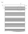
- FIG. 3 is an enlarged view of an "A" region ( FIG. 2 ) for illustrating the multiple structure of the quantum well layer 142.
- the quantum well layer 142 may include a plurality of sub-barrier layers 142a, and a plurality of sub-quantum well layers 142b aligned alternately with the sub-barrier layers 142a. That is, the sub-barrier layers 142a and the sub-quantum well layers 142b may be alternately stacked.
- the sub-barrier layers 142a may include a semiconductor material having the compositional formula of In x1 Ga 1-x1 N (0 ⁇ x1 ⁇ 0.1) and the sub-quantum well layers 142b may include a semiconductor material having the compositional formula of In x2 Ga 1-x2 N (0.1 ⁇ x2 ⁇ 1).
- the sub-barrier layer 142a may have a thickness of approximately 1 ⁇ to 4 ⁇ , and preferably 1 ⁇ to 2 ⁇ , and/or more preferably 1.5 ⁇ .
- the sub-quantum well layer 142b may have a thickness of approximately 0.5 ⁇ to 3 ⁇ , and preferably 0.5 ⁇ to 1.5 ⁇ , and/or more preferably 1 ⁇ .
- the stack structure including the sub-barrier layer 142a and the sub-quantum well layers 142b may be repeatedly formed five to fifteen times, and preferably ten times.
- the active layer 140 may have a thickness similar to an active layer of the light emitting device.
- the thickness, the number of stack structures and material of the sub-barrier layer 142a and the sub-quantum well layers 142b may vary depending on intensity and wavelength of light emitted from the light emitting device, although embodiments are not limited thereto.
- the quantum well layer 142 of the active layer 140 may include indium (In), and a greater amount of pits may be formed as a ratio (or amount) of indium (In) included in the quantum well layer 142 is increased so that a surface of the quantum well layer 142 is roughly formed.
- the quantum well layer 142 having the rough surface may cause leakage current, thereby degrading crystal property of semiconductor layers formed on the quantum well layer 142.
- the quantum well layer 142 may include the sub-barrier layers 142a and the sub-quantum well layers 142b, thereby reducing leakage current caused by the quantum well layer 142 having the rough surface.
- the sub-barrier layer 142a which has a smooth surface because it has a relatively smaller amount of indium (In), may be stacked on the sub-quantum well layer 142b to attenuate surface roughness of the sub-quantum well layer 142b.
- the sub-quantum well layer 142b may then be stacked again on the sub-barrier layer 142a, thereby reducing leakage current caused by the quantum well layer 142 having the rough surface.
- the second conductive semiconductor layer 150 may be formed on the active layer 140 with superior crystal property.
- indium (In) included in the sub-quantum well layers 142b may penetrate into the sub-barrier layers 142a.
- the indium (In) may be uniformly distributed in the quantum well layer 142 without being excessively included in the quantum well layer 142 so that light emitting efficiency of the light emitting device may be improved.
- FIG. 4 shows a band diagram of an active layer of a light emitting device. Other arrangements and configurations may also be provided.
- a bandgap of a region corresponding to at least one barrier layer 141 in the active layer 140 may be greater than a bandgap of a region corresponding to at least one quantum well layer 142 that includes the sub-barrier layers 142a and the sub-quantum well layers 142b.
- the amount of indium (In) included in the sub-barrier layers 142a may be smaller than the amount of indium (In) included in the sub-quantum well layers 142b even in the same quantum well layer 142, so the bandgap of the region corresponding to the sub-barrier layers 142a may be greater than the bandgap of the region corresponding to the sub-quantum well layers 142b.
- the bandgap may be repeatedly changed in the same quantum well layer 142 so that recombination probability of electrons and holes passing through the quantum well layer 142 may increase, and so that light emitting efficiency of the light emitting device may be improved.
- the quantum well layer 142 may be fabricated through metal organic chemical vapor deposition (MOCVD), chemical vapor deposition (CVD), plasma-enhanced chemical vapor deposition (PECVD), molecular beam epitaxy (MBE), and/or hydride vapor phase epitaxy (HVPE) scheme.
- MOCVD metal organic chemical vapor deposition
- CVD chemical vapor deposition
- PECVD plasma-enhanced chemical vapor deposition
- MBE molecular beam epitaxy
- HVPE hydride vapor phase epitaxy
- the quantum well layer 142 may be formed by injecting trimethyl gallium (TMGa) gas, trimethyl indium (TMIn) gas, ammonia (NH 3 ) gas, and/or nitrogen (N 2 ) gas into the chamber.
- TMGa trimethyl gallium
- TMIn trimethyl indium
- NH 3 ammonia
- N 2 nitrogen
- the growth temperature of the quantum well layer 142 may be approximately 680°C to 800°C, and preferably approximately 750°C to 770°C.
- a flow rate of the trimethyl indium (TMIn) gas injected into the chamber may vary depending on stacking sequence of the sub-quantum well layers 142b. For ease of convenience, the following description may be made based on the assumption that the sub-quantum well layers 142b are stacked by ten times and divided into first to tenth sub-quantum well layers according to the stacking sequence thereof.
- 500cc of TMIn gas may be injected into the chamber.
- other sub-quantum well layers may be stacked on the first sub-quantum well layer by sequentially reducing the amount of TMIn gas by 10cc according to the stacking sequence of the sub-quantum well layers.
- the first to tenth sub-quantum well layers may be formed by injecting TMIn gas into the chamber in the amount of 500cc, 490cc, 480cc, 470cc, 460cc, 450cc, 440cc, 430cc, 420cc, and 410cc, respectively.
- the flow rate of the TMIn gas injected into the chamber may be gradually reduced according to stacking sequence of the sub-quantum well layers 142b because the sub-quantum well layers 142b containing the indium (In) may be easily grown on the rough surface.
- the sub-quantum well layers 142b which are stacked later, may be grown on the rough surface due to the pits caused by the indium (In) so the sub-quantum well layers 142b may be easily grown as compared with the sub-quantum well layers 142b that are previously stacked.
- the flow rate of the TMIn may gradually reduce to form the sub-quantum well layers 142
- configurations and/or embodiments are not limited thereto.
- the flow rate of the TMIn may be gradually increased to form the sub-quantum well layers 142. If the sub-quantum well layers 142b have the same amount of indium (In), a same energy bandgap may be formed theoretically. However, the first sub-quantum well layer may have a greatest amount of indium (In) and the amount of indium (In) may be gradually decreased according to the stacking sequence of the sub-quantum well layers.
- the energy bandgap may be gradually widened so that the first to tenth sub-quantum well layers may generate wavelengths different from each other, causing degradation of color purity. Therefore, if the amount of indium (In) injected into the sub-quantum well layers 142b increases such that the sub-quantum well layers 142b have a same amount of indium (In), color purity may be improved.
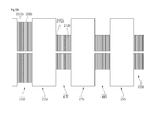
- FIG. 5A shows a band diagram of an active layer of a light emitting device according to an embodiment. Other embodiments and configurations may also be provided.
- FIG. 5A shows a plurality of quantum well layers 200, 210, 220 and 230 and a plurality of barrier layers 205, 215, 225.
- the sub-barrier layers 142a of the quantum well layer 200 (or the quantum well layer 142) adjacent to the first conductive semiconductor layer 130 may not include the indium (In) and the sub-quantum well layers 142b may include the indium (In). If the sub-barrier layers 142a do not include the indium (In), height of the bandgap of the sub-barrier layers 142a may be identical to height of the barrier layer 205, as shown in FIG. 5A .
- FIG. 5A also shows that a bandgap of the quantum well layer 210 is less than a bandgap of the quantum well layer 200 (and less than a bandgap of the barrier layer 205).
- the sub-barrier layers 142a of the quantum well layer 200 adjacent to the first conductive semiconductor layer 130 may not include the indium (In) having a lattice constant greater than gallium (Ga), a crystal property of the barrier layer may be improved so that leakage current can be minimized and reliability can be improved.
- the amount of indium included in the sub-barrier layers of one quantum well layer may be different from the amount of indium included in the sub-barrier layers of another quantum well layer.
- FIG. 5B shows the plurality of barrier layers 205, 215 and 225 as well as the plurality of quantum well layers 200, 210, 220 and 230.
- the quantum well layer 200 includes a plurality of sub-barrier layers 202a and a plurality of sub-quantum well layers 202b.
- the quantum well layer 210 includes a plurality of sub-barrier layer 212a and a plurality of sub-quantum well layer 212b.
- the amount of indium included in the sub-barrier layers 202a of the quantum well layer 200, which is closest to the first conductive semiconductor layer 130, may be different from the amount of indium included in the sub-barrier layers 212a of the quantum well layer 210. Additionally, the sub-barrier layers of one quantum well layer, which is closest to the first conductive semiconductor layer, may not include indium.
- a bandgap of the plurality of sub-quantum well layers 202b is larger than a bandgap of the plurality of sub-quantum well layers 212b.
- FIG. 5C shows a plurality of barrier layers 305, 315 and 325 and a plurality of quantum well layers 310, 320 and 330.
- Each of the barrier layers 305, 315 and 325 may include sub-barrier layers 305a and sub-quantum well layers 305b.
- a bandgap of the barrier layer 305 (having sub-barrier layers 305a and sub-quantum well layer 305b) may be greater than a bandgap of the quantum well layer 310 (or the quantum well layers 320, 330), as shown in FIG. 5C .
- FIG. 6 is a sectional view showing a lateral type light emitting device according to an embodiment. Other embodiments and configurations may also be provided.
- the lateral type light emitting device may include the substrate 110, the first conductive semiconductor layer 130 on the substrate 110, the active layer 140 on the first conductive semiconductor layer 130, the second conductive semiconductor layer 150 on the active layer 140, an electrode layer 151 on the second conductive semiconductor layer 150, a first electrode 131 on the first conductive semiconductor layer 130, and a second electrode 152 on the electrode layer 151.
- the light emitting device may be mesa-etched such that the first conductive semiconductor layer 130 may be exposed.
- the first electrode 131 may be formed on the first conductive semiconductor layer 130, and the electrode layer 151 and the second electrode 152 may be formed on the second conductive semiconductor layer 150, thereby forming the lateral type light emitting device.
- the first and second electrodes 131 and 152 may be coupled to an external power source to supply power to the lateral type light emitting device.
- the first and second electrodes 131 and 152 may be formed on or under the first and second conductive semiconductor layers 130 and 150, respectively.
- the first and second electrodes 131 and 152 may be formed on the first and second conductive semiconductor layers 130 and 150, respectively.
- the electrode layer 151 may include a transparent electrode layer and/or a reflective electrode layer.
- the transparent electrode layer may include one of ITO, IZO (In-ZnO), GZO (Ga-ZnO), AZO (AI-ZnO), AGZO (AI-Ga ZnO), IGZO (In-Ga ZnO), IrOx, RuOx, RuOx/ITO, Ni/IrOx/Au, Ni/IrOx/Au/ITO, and ZnO, although embodiments are not limited thereto.
- the reflective electrode layer may include at least one of Ag, AI, Pd, Pt, and Cu having higher reflective efficiency, and/or an alloy thereof, although embodiments are not limited thereto.
- FIG. 7 is a sectional view showing a vertical type light emitting device according to an embodiment. Other embodiments and configurations may also be provided.
- the vertical type light emitting device may include a conductive support member 160, a reflective electrode layer 155 on the conductive support member 160, the second conductive semiconductor layer 150 on the reflective electrode layer 155, the active layer 140 on the second conductive semiconductor layer 150, the first conductive semiconductor layer 130, and a third electrode 170 on the first conductive semiconductor layer 130.
- the vertical type light emitting device may include the first conductive semiconductor layer 130, the active layer 140 on the first conductive semiconductor layer 130, the second conductive semiconductor layer 150 on the active layer 140, the reflective electrode layer 155 on the second conductive semiconductor layer 150 and the conductive support member 160 on the reflective electrode layer 155.
- the substrate (not shown) may be removed and the third electrode 170 may be formed, thereby forming the vertical type light emitting device.
- the conductive support member 160 and the third electrode 170 may supply power to the vertical type light emitting device.
- the conductive support member 160 may include at least one selected from the group consisting of Ti, Cr, Ni, AI, Pt, Au, W, Cu, Mo and a semiconductor substrate doped with impurities.
- the reflective electrode layer 155 may include at least one of Ag, AI, Pd, Pt and Cu having a higher reflective efficiency, and/or an alloy thereof.
- the substrate may be removed through a laser lift off process and/or an etching process. After the substrate has been removed, the etching process may be performed to polish a surface of the first conductive semiconductor layer 130.
- the substrate may include at least one of Al 2 O 3 , SiC, GaAs, GaN, ZnO, Si, GaP, InP, and Ge, although embodiments are not limited thereto.
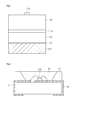
- FIG. 8 is a sectional view showing a light emitting device package having a light emitting device according to an embodiment. Other embodiments and configurations may also be provided.
- FIG. 8 shows that the light emitting device package may include a body 20, first and second electrode layers 31 and 32 formed on the body 20, the light emitting device 100 provided on the body 20 and a molding member 40 that surrounds the light emitting device 100.
- the light emitting device 100 may be electrically connected to the first and second electrode layers 31 and 32.
- the body 20 may include silicon, synthetic resin and/or a metallic material.
- An inclined surface may be formed around the light emitting device 100.
- the first and second electrode layers 31 and 32 may be electrically isolated from each other to supply power to the light emitting device 100. Additionally, the first and second electrode layers 31 and 32 may reflect the light emitted from the light emitting device 100 to improve light efficiency and dissipate heat generated from the light emitting device 100 to the outside.
- the light emitting device 100 may be provided on the body 20 and/or the first and second electrode layers 31 and 32.
- the light emitting device 100 is electrically coupled to the first and second electrode layers 31 and 32 through a wire, embodiments are not limited thereto.
- the light emitting device 100 may be electrically coupled to the first and second electrode layers 31 and 32 through a die bonding scheme or a flip chip scheme.
- the molding member 40 may surround the light emitting device 100 to protect the light emitting device 100. Additionally, the molding member 40 may include phosphors to change a wavelength of the light emitted from the light emitting device 100.
- FIG. 9 is an exploded perspective view showing a backlight unit including a light emitting device package according to an embodiment.
- the backlight unit may be an example of a lighting system, although embodiments are not limited thereto. Other embodiments and configurations may also be provided.
- a backlight unit 1100 may include a bottom frame 1140, a light guide member 1120 installed in the bottom frame 1140, and a light emitting module 1110 installed on at least one lateral side or bottom surface of the light guide member 1120. Additionally, a reflective sheet 1130 may be provided below the light guide member 1120.
- the bottom frame 1140 may have a box shape having a top surface being open to receive the light guide member 1120, the light emitting module 1110 and the reflective sheet 1130 therein. Additionally, the bottom frame 1140 may include a metallic material and/or a resin material, although embodiments are not limited thereto.
- the light emitting module 1110 may include a substrate 500 and a plurality of light emitting device packages 400 installed on the substrate.
- the light emitting device packages 400 may provide light to the light guide member 1120.
- the light emitting module 1110 may be installed on at least one inner side of the bottom frame 1140 to provide light to at least one side of the light guide member 1120.
- the light emitting module 1110 may be provided below the bottom frame 1140 to provide the light toward a bottom surface of the light guide member 1120. Such an arrangement may be variously changed according to design of the backlight unit 1100, although embodiments are not limited thereto.
- the light guide member 1120 may be provided in the bottom frame 1140.
- the light guide member 1120 may convert the light emitted from the light emitting module 1110 into surface light to guide surface light toward a display panel (not shown).
- the light guide member 1120 may include a light guide plate.
- the light guide plate may include one selected from the group consisting of acryl-based resin, such as PMMA (polymethyl methacrylate), PET (polyethylene terephthalate), PC (polycarbonate), COC and/or PEN (polyethylene naphthalate) resin.
- PMMA polymethyl methacrylate
- PET polyethylene terephthalate
- PC polycarbonate
- COC polycarbonate
- PEN polyethylene naphthalate
- An optical sheet 1150 may also be provided over the light guide member 1120.
- the optical sheet 1150 may include at least one of a diffusion sheet, a light collection sheet, a brightness enhancement sheet, and/or a fluorescent sheet.
- the optical sheet 1150 may have a stack structure of the diffusion sheet, the light collection sheet, the brightness enhancement sheet, and/or the fluorescent sheet.
- the diffusion sheet may uniformly diffuse the light emitted from the light emitting module 1110 such that the diffused light may be collected on the display panel by the light collection sheet.
- the light output from the light collection sheet may be randomly polarized and the brightness enhancement sheet may increase the degree of polarization of the light output from the light collection sheet.
- the light collection sheet may include a horizontal and/or vertical prism sheet.
- the brightness enhancement sheet may include a dual brightness enhancement film and the fluorescent sheet may include a transmittive plate or a transmittive film including phosphors.
- the reflective sheet 1130 may be provided below the light guide member 1120.
- the reflective sheet 1130 may reflect the light, emitted through the bottom surface of the light guide member 1120 toward the light exit surface of the light guide member 1120.
- the reflective sheet 1130 may include resin material having a high reflectivity, such as PET, PC or PVC resin, although embodiments are not limited thereto.
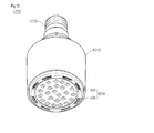
- FIG. 10 is a perspective view showing a lighting unit including a light emitting device package according to an embodiment. Other embodiments and configurations may also be provided.
- the lighting unit shown in FIG. 10 may be an example of a lighting system, although embodiments are not limited thereto.
- a lighting unit 1200 may include a case body 1210, a light emitting module 1230 installed in the case body 1210, and a connection terminal 1220 installed in the case body 1210 to receive power from an external power source.
- the case body 1210 may include material having superior heat dissipation property.
- the case body 1210 may include a metallic material or a resin material.
- the light emitting module 1230 may include a substrate 500 and at least one light emitting device package 400 installed on the substrate 500.
- the substrate 500 may include an insulating member printed with a circuit pattern.
- the substrate 500 may include a PCB (printed circuit board), an MC (metal core) PCB, an F (flexible) PCB, and/or a ceramic PCB.
- the substrate 500 may include a material that effectively reflects the light.
- the surface of the substrate 500 may be coated with a color, such as a white color or a silver color, to effectively reflect the light.
- At least one light emitting device package 400 may be installed on the substrate 500.
- Each light emitting device package 400 may include at least one light emitting diode (LED).
- the LED may include a colored LED that emits light having a color of red, green, blue or white and a UV (ultraviolet) LED that emits UV light.
- the LEDs of the light emitting module 1230 may be variously arranged to provide various colors and brightness.
- the white LED, the red LED and the green LED may be arranged to achieve a high color rendering index (CRI).
- a fluorescent sheet may be provided in a path of the light emitted from the light emitting module 1230 to change wavelength of the light emitted from the light emitting module 1230.
- the fluorescent sheet may include yellow phosphors. The light emitted from the light emitting module 1230 may pass through the fluorescent sheet so that the light is viewed as white light.
- connection terminal 1220 may be electrically connected to the light emitting module 1230 to supply power to the light emitting module 1230.
- the connection terminal 1220 may have a shape of a socket screw-coupled with the external power source, although embodiments are not limited thereto.
- the connection terminal 1220 may be prepared in the form of a pin inserted into the external power source or coupled to the external power source through a wire.
- At least one of a light guide member, a diffusion sheet, a light collection sheet, a brightness enhancement sheet and a fluorescent sheet may be provided in the path of the light emitted from the light emitting module, so that a desired optical effect can be achieved.
- An embodiment may provide a light emitting device having a novel structure, a light emitting device package, a method of manufacturing the light emitting device, and/or a lighting system.
- An embodiment may provide a light emitting device capable of improving light emitting efficiency, a light emitting device package, a method of manufacturing the light emitting device, and/or a lighting system.
- An embodiment may provide a light emitting device capable of reducing leakage current and a method of manufacturing the same.
- a light emitting device may include a first conductive semiconductor layer, an active layer including at least one barrier layer and at least one quantum well layer stacked on the first conductive semiconductor layer, and a second conductive semiconductor layer on the active layer.
- the at least one quantum well layer may include a plurality of sub-barrier layers, which are divided into first to n th sub-barrier layers sequentially stacked from the first sub-barrier layer, and a plurality of sub-quantum well layers, which are divided into first to n th sub-quantum well layers sequentially stacked from the first sub-quantum well layer and have bandgaps lower than bandgaps of the sub-barrier layers, and wherein the sub-quantum well layers have a region where a ratio of indium (In) injected into the sub-quantum well layers is increased according to a stacking sequence of the sub-quantum well layers.
- a method of manufacturing a light emitting device may include forming a first conductive semiconductor layer, forming an active layer including at least one barrier layer and at least one quantum well layer alternately stacked on the first conductive semiconductor layer by injecting at least one of trimethyl gallium (TMGa) gas, trimethyl indium (TMln) gas, ammonia (NH 3 ) gas and nitrogen (N 2 ) gas into a chamber through a metal organic chemical vapor deposition (MOCVD) process, and forming a second conductive semiconductor layer on the active layer.
- TMGa trimethyl gallium
- TMln trimethyl indium
- NH 3 ammonia
- N 2 nitrogen
- the at least one quantum well layer may include a plurality of sub-barrier layers and a plurality of sub-quantum well layers having a region where a ratio of TMIn gas injected into a chamber increases according to a stacking sequence of the sub-quantum well layers.
- a light emitting device package may include a package body, first and second electrode layers on the package body, and a light emitting device electrically coupled to the first and second electrode layers.
- the light emitting device may include a first conductive semiconductor layer, an active layer including at least one barrier layer and at least one quantum well layer stacked on the first conductive semiconductor layer, and a second conductive semiconductor layer on the active layer.
- the at least one quantum well layer may include a plurality of sub-barrier layers, which are divided into first to n th sub-barrier layers sequentially stacked from the first sub-barrier layer, and a plurality of sub-quantum well layers, which are divided into first to n th sub-quantum well layers sequentially stacked from the first sub-quantum well layer and have bandgaps lower than bandgaps of the sub-barrier layers.
- the sub-quantum well layers may have a region where a ratio of indium (In) injected into the sub-quantum well layers increases according to a stacking sequence of the sub-quantum well layers.
- a lighting system may include a light emitting module that includes a substrate and a light emitting device installed on the substrate, wherein the light emitting device comprises: a first conductive semiconductor layer, an active layer including at least one barrier layer and at least one quantum well layer stacked on the first conductive semiconductor layer, and a second conductive semiconductor layer on the active layer.
- the at least one quantum well layer may include a plurality of sub-barrier layers, which are divided into first to n th sub-barrier layers sequentially stacked from the first sub-barrier layer, and a plurality of sub-quantum well layers, which are divided into first to n th sub-quantum well layers sequentially stacked from the first sub-quantum well layer and have bandgaps lower than bandgaps of the sub-barrier layers, and wherein the sub-quantum well layers have a region where a ratio of indium (In) injected into the sub-quantum well layers increases according to a stacking sequence of the sub-quantum well layers.
- In indium
- any reference in this specification to "one embodiment,” “an embodiment,” “example embodiment,” etc. means that a particular feature, structure, or characteristic described in connection with the embodiment is included in at least one embodiment of the invention.
- the appearances of such phrases in various places in the specification are not necessarily all referring to the same embodiment.
Landscapes
- Engineering & Computer Science (AREA)
- Manufacturing & Machinery (AREA)
- Computer Hardware Design (AREA)
- Microelectronics & Electronic Packaging (AREA)
- Power Engineering (AREA)
- Led Devices (AREA)
- Non-Portable Lighting Devices Or Systems Thereof (AREA)
- Led Device Packages (AREA)
Abstract
Description
- Embodiments may relate to a light emitting device.
- A light emitting diode (LED) is a semiconductor light emitting device that converts current into light. The LED has been employed as a light source for a display device, a vehicle, and/or a lighting device. Additionally, the LED may represent a white color having superior light efficiency by employing phosphors and/or combining LEDs having various colors.
- In order to improve brightness and/or performance of the LED, attempts have been performed to improve a light extraction structure, an active layer structure, a current diffusion, an electrode structure, and a structure of a light emitting diode package.
- Arrangements and embodiments may be described in detail with reference to the following drawings in which like reference numerals refer to like elements and wherein:
-
FIG. 1 is a sectional view showing a light emitting device according to an embodiment; -
FIG. 2 is a sectional view showing an active layer of a light emitting device according to an embodiment; -
FIG. 3 is an enlarged view of an "A" region (FIG. 2 ); -
FIG. 4 is a band diagram of an active layer of a light emitting device; -
FIGs. 5A-5C are band diagrams of an active layer of a light emitting device according to embodiments; -
FIG. 6 is a sectional view showing a lateral type light emitting device according to an embodiment; -
FIG. 7 is a sectional view showing a vertical type light emitting device according to an embodiment; -
FIG. 8 is a sectional view showing a light emitting device package including a light emitting device according to an embodiment; -
FIG. 9 is an exploded perspective view showing a backlight unit including a light emitting device or a light emitting device package according to an embodiment; and -
FIG. 10 is a perspective view showing a lighting unit including a light emitting device or a light emitting device package according to an embodiment. - In the following description, it is understood that when a layer (or film), a region, a pattern, and/or a structure is referred to as being "on", "under" or "adjacent" another substrate, another layer (or film), another region, another pad, and/or another pattern, it may be "directly" or "indirectly" on the other substrate, layer (or film), region, pad, and/or pattern, and/or one or more intervening layers may also be present. Such a position of the layer may be described with reference to the drawings.
- Thickness and size of each layer shown in the drawings may be exaggerated, omitted and/or schematically drawn for ease of convenience or clarity. Additionally, the size of elements may not reflect an actual size.
- A light emitting device, a light emitting device package, a method of manufacturing the light emitting device, and a lighting system according to embodiments may be described with reference to the accompanying drawings.
-
FIG. 1 is a sectional view showing a light emitting device according to an embodiment.FIG. 2 is a sectional view showing anactive layer 140 of a light emitting device according to an embodiment. Other embodiments and configurations are also within the scope of embodiments. - As shown in
FIGs. 1 and2 , alight emitting device 100 may include asubstrate 110, a firstconductive semiconductor layer 130 on thesubstrate 110, anactive layer 140 on the firstconductive semiconductor layer 130, and a secondconductive semiconductor layer 150 on theactive layer 140. - The first
conductive semiconductor layer 130, theactive layer 140 and the secondconductive semiconductor layer 150 may form a light emitting structure for generating light. - The
substrate 110 may include at least one selected from the group consisting of Al2O3, SiC, Si, GaAs, GaN, ZnO, Si, GaP, InP, and Ge, although embodiments are not limited thereto. - The first
conductive semiconductor layer 130, theactive layer 140 and the secondconductive semiconductor layer 150 may be sequentially formed on thesubstrate 110 through metal organic chemical vapor deposition (MOCVD), chemical vapor deposition (CVD), plasma-enhanced chemical vapor deposition (PECVD), molecular beam epitaxy (MBE), and/or hydride vapor phase epitaxy (HVPE) scheme, although embodiments are not limited thereto. - For example, the first
conductive semiconductor layer 130 may include an n type semiconductor layer. The n type semiconductor layer may include semiconductor material having a compositional formula of InxAlyGa1-x-yN(0≤x≤1, 0 ≤y≤1, 0≤x+y≤1). For example, the n type semiconductor layer may include one selected from the group consisting of InAIGaN, GaN, AIGaN, InGaN, AIN, and InN. Additionally, the n type semiconductor layer may be doped with n type dopant, such as Si, Ge and/or Sn. - If the first
conductive semiconductor layer 130 is formed through the MOCVD scheme, the firstconductive semiconductor layer 130 may be formed by injecting at least one of trimethyl gallium (TMGa) gas, trimethyl indium (TMIn) gas, trimethyl aluminum (TMAI) gas, ammonia (NH3) gas, nitrogen (N2) gas and hydrogen (H2) gas into a chamber together with silane (SiH4) gas including n type dopant, such as Si, although embodiments are not limited thereto. - A buffer layer (not shown) and an undoped semiconductor layer (not shown) may be formed between the first
conductive semiconductor layer 130 and thesubstrate 110 to attenuate lattice mismatch between the firstconductive semiconductor layer 130 and thesubstrate 110. - The buffer layer may include a semiconductor material having the compositional formula of InxAlyGa1-x-yN (0≤x≤1, 0 ≤y≤1, 0≤x+y≤1). 0 For example, the buffer layer may include one of InAlGaN, GaN, AlGaN, InGaN, AlN, and/or InN.
- The undoped semiconductor layer may include a semiconductor material having the compositional formula of InxAlyGa1-x-yN (0≤x≤1, 0 ≤y≤1, 0≤x+y≤1). For example, the undoped semiconductor layer may include an undoped GaN layer, although embodiments are not limited thereto.
- The
active layer 140 may be formed on the firstconductive semiconductor layer 130. - Electrons (or holes) injected through the first
conductive semiconductor layer 130 may be recombined with the holes (or electrons) injected through the secondconductive semiconductor layer 150 at theactive layer 140 while generating energy so that theactive layer 140 may emit light. - The
active layer 140 may include a semiconductor material having the compositional formula of InxAlyGa1-x-yN (0≤x≤1, 0 ≤y≤1, 0≤x+y≤1). Additionally, theactive layer 140 may have a single quantum well structure, a multiple quantum well (MQW) structure, and/or a quantum dot structure. According to this embodiment, theactive layer 140 may have the multiple quantum well (MQW) structure. - As shown in
FIG. 2 , if theactive layer 140 has the MQW structure or the single quantum well structure, theactive layer 140 may have at least onebarrier layer 141 and at least onequantum well layer 142. That is, theactive layer 140 may have a stack structure including at least onebarrier layer 141 and at least onequantum well layer 142 that are alternately stacked. - The stack structure including at least one
barrier layer 141 and at least onequantum well layer 142 may be repeatedly formed by five to ten times, and preferably seven times. - The
barrier layer 141 may have a thickness of approximately 80Å to 120Å, and/or preferably 100Å. Thequantum well layer 142 may have a thickness of approximately 20Å to 30Å, and preferably 250Å. Thus, theactive layer 140 may have a total thickness of approximately 800Å to 1500Å. - If the
active layer 140 is formed through the MOCVD scheme, theactive layer 140 may be formed by injecting trimethyl gallium (TMGa) gas, trimethyl indium (TMIn) gas, ammonia (NH3) gas, and/or nitrogen (N2) gas into a chamber such that theactive layer 140 may have the MQW structure in which at least onebarrier layer 141 and at least onequantum well layer 142 are prepared as the InGaN/GaN structure, although embodiments are not limited thereto. - Since at least one
barrier layer 141 and at least onequantum well layer 142 are provided, recombination probability of electrons and holes may be increased as compared with the single quantum well structure so that light emitting efficiency of the light emitting device may be improved. - According to this embodiment, the at least one
quantum well layer 142 may have a multiple structure. Thequantum well layer 142 having the multiple structure and method of manufacturing the same may be described below in detail. -
FIG. 3 is an enlarged view of an "A" region (FIG. 2 ) for illustrating the multiple structure of thequantum well layer 142. - The
quantum well layer 142 may include a plurality ofsub-barrier layers 142a, and a plurality of sub-quantumwell layers 142b aligned alternately with thesub-barrier layers 142a. That is, thesub-barrier layers 142a and the sub-quantumwell layers 142b may be alternately stacked. - For example, the
sub-barrier layers 142a may include a semiconductor material having the compositional formula of Inx1Ga1-x1N (0≤x1≤0.1) and thesub-quantum well layers 142b may include a semiconductor material having the compositional formula of Inx2Ga1-x2N (0.1≤x2<1). - The
sub-barrier layer 142a may have a thickness of approximately 1Å to 4Å, and preferably 1Å to 2Å, and/or more preferably 1.5Å. Thesub-quantum well layer 142b may have a thickness of approximately 0.5Å to 3Å, and preferably 0.5Å to 1.5Å, and/or more preferably 1Å. - The stack structure including the
sub-barrier layer 142a and the sub-quantumwell layers 142b may be repeatedly formed five to fifteen times, and preferably ten times. - Since the
sub-barrier layer 142a and the sub-quantum well layers 142b having the above thickness may be repeatedly formed, theactive layer 140 may have a thickness similar to an active layer of the light emitting device. - The thickness, the number of stack structures and material of the
sub-barrier layer 142a and the sub-quantumwell layers 142b may vary depending on intensity and wavelength of light emitted from the light emitting device, although embodiments are not limited thereto. - The
quantum well layer 142 of theactive layer 140 may include indium (In), and a greater amount of pits may be formed as a ratio (or amount) of indium (In) included in thequantum well layer 142 is increased so that a surface of thequantum well layer 142 is roughly formed. Thequantum well layer 142 having the rough surface may cause leakage current, thereby degrading crystal property of semiconductor layers formed on thequantum well layer 142. - The
quantum well layer 142 may include thesub-barrier layers 142a and the sub-quantumwell layers 142b, thereby reducing leakage current caused by thequantum well layer 142 having the rough surface. - After forming the
sub-quantum well layer 142b, thesub-barrier layer 142a, which has a smooth surface because it has a relatively smaller amount of indium (In), may be stacked on thesub-quantum well layer 142b to attenuate surface roughness of thesub-quantum well layer 142b. Thesub-quantum well layer 142b may then be stacked again on thesub-barrier layer 142a, thereby reducing leakage current caused by thequantum well layer 142 having the rough surface. - Since surface roughness of the
quantum well layer 142 is attenuated, the secondconductive semiconductor layer 150 may be formed on theactive layer 140 with superior crystal property. - Additionally, since the sub-quantum well layers 142b and the
sub-barrier layers 142a may be alternately stacked, indium (In) included in the sub-quantumwell layers 142b may penetrate into thesub-barrier layers 142a. As a result, the indium (In) may be uniformly distributed in thequantum well layer 142 without being excessively included in thequantum well layer 142 so that light emitting efficiency of the light emitting device may be improved. -
FIG. 4 shows a band diagram of an active layer of a light emitting device. Other arrangements and configurations may also be provided. - As shown in
FIG. 4 , a bandgap of a region corresponding to at least onebarrier layer 141 in theactive layer 140 may be greater than a bandgap of a region corresponding to at least onequantum well layer 142 that includes thesub-barrier layers 142a and the sub-quantum well layers 142b. - The amount of indium (In) included in the
sub-barrier layers 142a may be smaller than the amount of indium (In) included in the sub-quantum well layers 142b even in the samequantum well layer 142, so the bandgap of the region corresponding to thesub-barrier layers 142a may be greater than the bandgap of the region corresponding to the sub-quantum well layers 142b. - Referring to the band diagram for the light emitting device, the bandgap may be repeatedly changed in the same quantum well layer 142 so that recombination probability of electrons and holes passing through the
quantum well layer 142 may increase, and so that light emitting efficiency of the light emitting device may be improved. - Similar to other semiconductor layers, the
quantum well layer 142 may be fabricated through metal organic chemical vapor deposition (MOCVD), chemical vapor deposition (CVD), plasma-enhanced chemical vapor deposition (PECVD), molecular beam epitaxy (MBE), and/or hydride vapor phase epitaxy (HVPE) scheme. - If the
quantum well layer 142 is formed through the MOCVD scheme, thequantum well layer 142 may be formed by injecting trimethyl gallium (TMGa) gas, trimethyl indium (TMIn) gas, ammonia (NH3) gas, and/or nitrogen (N2) gas into the chamber. The growth temperature of thequantum well layer 142 may be approximately 680°C to 800°C, and preferably approximately 750°C to 770°C. - A flow rate of the trimethyl indium (TMIn) gas injected into the chamber may vary depending on stacking sequence of the sub-quantum well layers 142b. For ease of convenience, the following description may be made based on the assumption that the sub-quantum
well layers 142b are stacked by ten times and divided into first to tenth sub-quantum well layers according to the stacking sequence thereof. - For example, when the first sub-quantum well layer is grown, 500cc of TMIn gas may be injected into the chamber. Additionally, other sub-quantum well layers may be stacked on the first sub-quantum well layer by sequentially reducing the amount of TMIn gas by 10cc according to the stacking sequence of the sub-quantum well layers. The first to tenth sub-quantum well layers may be formed by injecting TMIn gas into the chamber in the amount of 500cc, 490cc, 480cc, 470cc, 460cc, 450cc, 440cc, 430cc, 420cc, and 410cc, respectively.
- The flow rate of the TMIn gas injected into the chamber may be gradually reduced according to stacking sequence of the sub-quantum well layers 142b because the sub-quantum well layers 142b containing the indium (In) may be easily grown on the rough surface.
- In other words, the sub-quantum
well layers 142b, which are stacked later, may be grown on the rough surface due to the pits caused by the indium (In) so the sub-quantumwell layers 142b may be easily grown as compared with the sub-quantum well layers 142b that are previously stacked. - Although it has been described that the flow rate of the TMIn may gradually reduce to form the sub-quantum well layers 142, configurations and/or embodiments are not limited thereto. Additionally, the flow rate of the TMIn may be gradually increased to form the sub-quantum well layers 142. If the sub-quantum
well layers 142b have the same amount of indium (In), a same energy bandgap may be formed theoretically. However, the first sub-quantum well layer may have a greatest amount of indium (In) and the amount of indium (In) may be gradually decreased according to the stacking sequence of the sub-quantum well layers. Thus, the energy bandgap may be gradually widened so that the first to tenth sub-quantum well layers may generate wavelengths different from each other, causing degradation of color purity. Therefore, if the amount of indium (In) injected into the sub-quantum well layers 142b increases such that the sub-quantumwell layers 142b have a same amount of indium (In), color purity may be improved. -
FIG. 5A shows a band diagram of an active layer of a light emitting device according to an embodiment. Other embodiments and configurations may also be provided. -
FIG. 5A shows a plurality of quantum well layers 200, 210, 220 and 230 and a plurality of barrier layers 205, 215, 225. - The sub-barrier layers 142a of the quantum well layer 200 (or the quantum well layer 142) adjacent to the first
conductive semiconductor layer 130 may not include the indium (In) and the sub-quantumwell layers 142b may include the indium (In). If thesub-barrier layers 142a do not include the indium (In), height of the bandgap of thesub-barrier layers 142a may be identical to height of thebarrier layer 205, as shown inFIG. 5A . -
FIG. 5A also shows that a bandgap of thequantum well layer 210 is less than a bandgap of the quantum well layer 200 (and less than a bandgap of the barrier layer 205). - Since the
sub-barrier layers 142a of thequantum well layer 200 adjacent to the firstconductive semiconductor layer 130 may not include the indium (In) having a lattice constant greater than gallium (Ga), a crystal property of the barrier layer may be improved so that leakage current can be minimized and reliability can be improved. - The amount of indium included in the sub-barrier layers of one quantum well layer may be different from the amount of indium included in the sub-barrier layers of another quantum well layer.
- For example,
FIG. 5B shows the plurality of barrier layers 205, 215 and 225 as well as the plurality of quantum well layers 200, 210, 220 and 230. As shown inFIG. 5B , thequantum well layer 200 includes a plurality ofsub-barrier layers 202a and a plurality of sub-quantumwell layers 202b. Thequantum well layer 210 includes a plurality ofsub-barrier layer 212a and a plurality ofsub-quantum well layer 212b. - The amount of indium included in the
sub-barrier layers 202a of thequantum well layer 200, which is closest to the firstconductive semiconductor layer 130, may be different from the amount of indium included in thesub-barrier layers 212a of thequantum well layer 210. Additionally, the sub-barrier layers of one quantum well layer, which is closest to the first conductive semiconductor layer, may not include indium. - As shown in
FIG. 5B , a bandgap of the plurality of sub-quantumwell layers 202b is larger than a bandgap of the plurality of sub-quantumwell layers 212b. -
FIG. 5C shows a plurality of barrier layers 305, 315 and 325 and a plurality of quantum well layers 310, 320 and 330. Each of the barrier layers 305, 315 and 325 may includesub-barrier layers 305a and sub-quantumwell layers 305b. A bandgap of the barrier layer 305 (havingsub-barrier layers 305a andsub-quantum well layer 305b) may be greater than a bandgap of the quantum well layer 310 (or the quantum well layers 320, 330), as shown inFIG. 5C . -
FIG. 6 is a sectional view showing a lateral type light emitting device according to an embodiment. Other embodiments and configurations may also be provided. - As shown in
FIG. 6 , the lateral type light emitting device may include thesubstrate 110, the firstconductive semiconductor layer 130 on thesubstrate 110, theactive layer 140 on the firstconductive semiconductor layer 130, the secondconductive semiconductor layer 150 on theactive layer 140, anelectrode layer 151 on the secondconductive semiconductor layer 150, afirst electrode 131 on the firstconductive semiconductor layer 130, and asecond electrode 152 on theelectrode layer 151. - The light emitting device may be mesa-etched such that the first
conductive semiconductor layer 130 may be exposed. Thefirst electrode 131 may be formed on the firstconductive semiconductor layer 130, and theelectrode layer 151 and thesecond electrode 152 may be formed on the secondconductive semiconductor layer 150, thereby forming the lateral type light emitting device. - The first and
second electrodes second electrodes second electrodes - The
electrode layer 151 may include a transparent electrode layer and/or a reflective electrode layer. - The transparent electrode layer may include one of ITO, IZO (In-ZnO), GZO (Ga-ZnO), AZO (AI-ZnO), AGZO (AI-Ga ZnO), IGZO (In-Ga ZnO), IrOx, RuOx, RuOx/ITO, Ni/IrOx/Au, Ni/IrOx/Au/ITO, and ZnO, although embodiments are not limited thereto.
- The reflective electrode layer may include at least one of Ag, AI, Pd, Pt, and Cu having higher reflective efficiency, and/or an alloy thereof, although embodiments are not limited thereto.
-
FIG. 7 is a sectional view showing a vertical type light emitting device according to an embodiment. Other embodiments and configurations may also be provided. - As shown in
FIG. 7 , the vertical type light emitting device may include aconductive support member 160, areflective electrode layer 155 on theconductive support member 160, the secondconductive semiconductor layer 150 on thereflective electrode layer 155, theactive layer 140 on the secondconductive semiconductor layer 150, the firstconductive semiconductor layer 130, and athird electrode 170 on the firstconductive semiconductor layer 130. - When viewed from another direction, the vertical type light emitting device may include the first
conductive semiconductor layer 130, theactive layer 140 on the firstconductive semiconductor layer 130, the secondconductive semiconductor layer 150 on theactive layer 140, thereflective electrode layer 155 on the secondconductive semiconductor layer 150 and theconductive support member 160 on thereflective electrode layer 155. - After forming the
reflective electrode layer 155 and theconductive support member 160 on the light emitting device, the substrate (not shown) may be removed and thethird electrode 170 may be formed, thereby forming the vertical type light emitting device. - The
conductive support member 160 and thethird electrode 170 may supply power to the vertical type light emitting device. - The
conductive support member 160 may include at least one selected from the group consisting of Ti, Cr, Ni, AI, Pt, Au, W, Cu, Mo and a semiconductor substrate doped with impurities. - The
reflective electrode layer 155 may include at least one of Ag, AI, Pd, Pt and Cu having a higher reflective efficiency, and/or an alloy thereof. - The substrate may be removed through a laser lift off process and/or an etching process. After the substrate has been removed, the etching process may be performed to polish a surface of the first
conductive semiconductor layer 130. The substrate may include at least one of Al2O3, SiC, GaAs, GaN, ZnO, Si, GaP, InP, and Ge, although embodiments are not limited thereto. - Light Emitting Device Package
-
FIG. 8 is a sectional view showing a light emitting device package having a light emitting device according to an embodiment. Other embodiments and configurations may also be provided. -
FIG. 8 shows that the light emitting device package may include abody 20, first and second electrode layers 31 and 32 formed on thebody 20, thelight emitting device 100 provided on thebody 20 and amolding member 40 that surrounds thelight emitting device 100. Thelight emitting device 100 may be electrically connected to the first and second electrode layers 31 and 32. - The
body 20 may include silicon, synthetic resin and/or a metallic material. An inclined surface may be formed around thelight emitting device 100. - The first and second electrode layers 31 and 32 may be electrically isolated from each other to supply power to the
light emitting device 100. Additionally, the first and second electrode layers 31 and 32 may reflect the light emitted from thelight emitting device 100 to improve light efficiency and dissipate heat generated from thelight emitting device 100 to the outside. - The
light emitting device 100 may be provided on thebody 20 and/or the first and second electrode layers 31 and 32. - Although it is shown that the
light emitting device 100 is electrically coupled to the first and second electrode layers 31 and 32 through a wire, embodiments are not limited thereto. For example, thelight emitting device 100 may be electrically coupled to the first and second electrode layers 31 and 32 through a die bonding scheme or a flip chip scheme. - The
molding member 40 may surround thelight emitting device 100 to protect thelight emitting device 100. Additionally, the moldingmember 40 may include phosphors to change a wavelength of the light emitted from thelight emitting device 100. -
FIG. 9 is an exploded perspective view showing a backlight unit including a light emitting device package according to an embodiment. The backlight unit may be an example of a lighting system, although embodiments are not limited thereto. Other embodiments and configurations may also be provided. - As shown in
FIG. 9 , abacklight unit 1100 may include abottom frame 1140, alight guide member 1120 installed in thebottom frame 1140, and alight emitting module 1110 installed on at least one lateral side or bottom surface of thelight guide member 1120. Additionally, areflective sheet 1130 may be provided below thelight guide member 1120. - The
bottom frame 1140 may have a box shape having a top surface being open to receive thelight guide member 1120, thelight emitting module 1110 and thereflective sheet 1130 therein. Additionally, thebottom frame 1140 may include a metallic material and/or a resin material, although embodiments are not limited thereto. - The
light emitting module 1110 may include asubstrate 500 and a plurality of light emitting device packages 400 installed on the substrate. The light emitting device packages 400 may provide light to thelight guide member 1120. - As shown in
FIG. 9 , thelight emitting module 1110 may be installed on at least one inner side of thebottom frame 1140 to provide light to at least one side of thelight guide member 1120. - Additionally, the
light emitting module 1110 may be provided below thebottom frame 1140 to provide the light toward a bottom surface of thelight guide member 1120. Such an arrangement may be variously changed according to design of thebacklight unit 1100, although embodiments are not limited thereto. - The
light guide member 1120 may be provided in thebottom frame 1140. Thelight guide member 1120 may convert the light emitted from thelight emitting module 1110 into surface light to guide surface light toward a display panel (not shown). - The
light guide member 1120 may include a light guide plate. For example, the light guide plate may include one selected from the group consisting of acryl-based resin, such as PMMA (polymethyl methacrylate), PET (polyethylene terephthalate), PC (polycarbonate), COC and/or PEN (polyethylene naphthalate) resin. - An
optical sheet 1150 may also be provided over thelight guide member 1120. - The
optical sheet 1150 may include at least one of a diffusion sheet, a light collection sheet, a brightness enhancement sheet, and/or a fluorescent sheet. For example, theoptical sheet 1150 may have a stack structure of the diffusion sheet, the light collection sheet, the brightness enhancement sheet, and/or the fluorescent sheet. The diffusion sheet may uniformly diffuse the light emitted from thelight emitting module 1110 such that the diffused light may be collected on the display panel by the light collection sheet. The light output from the light collection sheet may be randomly polarized and the brightness enhancement sheet may increase the degree of polarization of the light output from the light collection sheet. The light collection sheet may include a horizontal and/or vertical prism sheet. Additionally, the brightness enhancement sheet may include a dual brightness enhancement film and the fluorescent sheet may include a transmittive plate or a transmittive film including phosphors. - The
reflective sheet 1130 may be provided below thelight guide member 1120. Thereflective sheet 1130 may reflect the light, emitted through the bottom surface of thelight guide member 1120 toward the light exit surface of thelight guide member 1120. - The
reflective sheet 1130 may include resin material having a high reflectivity, such as PET, PC or PVC resin, although embodiments are not limited thereto. -
FIG. 10 is a perspective view showing a lighting unit including a light emitting device package according to an embodiment. Other embodiments and configurations may also be provided. The lighting unit shown inFIG. 10 may be an example of a lighting system, although embodiments are not limited thereto. - As shown in
FIG. 10 , a lighting unit 1200 may include acase body 1210, alight emitting module 1230 installed in thecase body 1210, and aconnection terminal 1220 installed in thecase body 1210 to receive power from an external power source. - The
case body 1210 may include material having superior heat dissipation property. For example, thecase body 1210 may include a metallic material or a resin material. - The
light emitting module 1230 may include asubstrate 500 and at least one light emittingdevice package 400 installed on thesubstrate 500. - The
substrate 500 may include an insulating member printed with a circuit pattern. For example, thesubstrate 500 may include a PCB (printed circuit board), an MC (metal core) PCB, an F (flexible) PCB, and/or a ceramic PCB. - Additionally, the
substrate 500 may include a material that effectively reflects the light. The surface of thesubstrate 500 may be coated with a color, such as a white color or a silver color, to effectively reflect the light. - At least one light emitting
device package 400 may be installed on thesubstrate 500. Each light emittingdevice package 400 may include at least one light emitting diode (LED). The LED may include a colored LED that emits light having a color of red, green, blue or white and a UV (ultraviolet) LED that emits UV light. - The LEDs of the
light emitting module 1230 may be variously arranged to provide various colors and brightness. For example, the white LED, the red LED and the green LED may be arranged to achieve a high color rendering index (CRI). Additionally, a fluorescent sheet may be provided in a path of the light emitted from thelight emitting module 1230 to change wavelength of the light emitted from thelight emitting module 1230. For example, if the light emitted from thelight emitting module 1230 has a wavelength band of blue light, the fluorescent sheet may include yellow phosphors. The light emitted from thelight emitting module 1230 may pass through the fluorescent sheet so that the light is viewed as white light. - The
connection terminal 1220 may be electrically connected to thelight emitting module 1230 to supply power to thelight emitting module 1230. Theconnection terminal 1220 may have a shape of a socket screw-coupled with the external power source, although embodiments are not limited thereto. For example, theconnection terminal 1220 may be prepared in the form of a pin inserted into the external power source or coupled to the external power source through a wire. - According to the illumination system discussed above, at least one of a light guide member, a diffusion sheet, a light collection sheet, a brightness enhancement sheet and a fluorescent sheet may be provided in the path of the light emitted from the light emitting module, so that a desired optical effect can be achieved.
- An embodiment may provide a light emitting device having a novel structure, a light emitting device package, a method of manufacturing the light emitting device, and/or a lighting system.
- An embodiment may provide a light emitting device capable of improving light emitting efficiency, a light emitting device package, a method of manufacturing the light emitting device, and/or a lighting system.
- An embodiment may provide a light emitting device capable of reducing leakage current and a method of manufacturing the same.
- A light emitting device may include a first conductive semiconductor layer, an active layer including at least one barrier layer and at least one quantum well layer stacked on the first conductive semiconductor layer, and a second conductive semiconductor layer on the active layer. The at least one quantum well layer may include a plurality of sub-barrier layers, which are divided into first to nth sub-barrier layers sequentially stacked from the first sub-barrier layer, and a plurality of sub-quantum well layers, which are divided into first to nth sub-quantum well layers sequentially stacked from the first sub-quantum well layer and have bandgaps lower than bandgaps of the sub-barrier layers, and wherein the sub-quantum well layers have a region where a ratio of indium (In) injected into the sub-quantum well layers is increased according to a stacking sequence of the sub-quantum well layers.
- A method of manufacturing a light emitting device may include forming a first conductive semiconductor layer, forming an active layer including at least one barrier layer and at least one quantum well layer alternately stacked on the first conductive semiconductor layer by injecting at least one of trimethyl gallium (TMGa) gas, trimethyl indium (TMln) gas, ammonia (NH3) gas and nitrogen (N2) gas into a chamber through a metal organic chemical vapor deposition (MOCVD) process, and forming a second conductive semiconductor layer on the active layer. The at least one quantum well layer may include a plurality of sub-barrier layers and a plurality of sub-quantum well layers having a region where a ratio of TMIn gas injected into a chamber increases according to a stacking sequence of the sub-quantum well layers.
- A light emitting device package may include a package body, first and second electrode layers on the package body, and a light emitting device electrically coupled to the first and second electrode layers. The light emitting device may include a first conductive semiconductor layer, an active layer including at least one barrier layer and at least one quantum well layer stacked on the first conductive semiconductor layer, and a second conductive semiconductor layer on the active layer. The at least one quantum well layer may include a plurality of sub-barrier layers, which are divided into first to nth sub-barrier layers sequentially stacked from the first sub-barrier layer, and a plurality of sub-quantum well layers, which are divided into first to nth sub-quantum well layers sequentially stacked from the first sub-quantum well layer and have bandgaps lower than bandgaps of the sub-barrier layers. The sub-quantum well layers may have a region where a ratio of indium (In) injected into the sub-quantum well layers increases according to a stacking sequence of the sub-quantum well layers.
- A lighting system may include a light emitting module that includes a substrate and a light emitting device installed on the substrate, wherein the light emitting device comprises: a first conductive semiconductor layer, an active layer including at least one barrier layer and at least one quantum well layer stacked on the first conductive semiconductor layer, and a second conductive semiconductor layer on the active layer. The at least one quantum well layer may include a plurality of sub-barrier layers, which are divided into first to nth sub-barrier layers sequentially stacked from the first sub-barrier layer, and a plurality of sub-quantum well layers, which are divided into first to nth sub-quantum well layers sequentially stacked from the first sub-quantum well layer and have bandgaps lower than bandgaps of the sub-barrier layers, and wherein the sub-quantum well layers have a region where a ratio of indium (In) injected into the sub-quantum well layers increases according to a stacking sequence of the sub-quantum well layers.
- Any reference in this specification to "one embodiment," "an embodiment," "example embodiment," etc., means that a particular feature, structure, or characteristic described in connection with the embodiment is included in at least one embodiment of the invention. The appearances of such phrases in various places in the specification are not necessarily all referring to the same embodiment. Further, when a particular feature, structure, or characteristic is described in connection with any embodiment, it is submitted that it is within the purview of one skilled in the art to effect such feature, structure, or characteristic in connection with other ones of the embodiments.
- Although embodiments have been described with reference to a number of illustrative embodiments thereof, it should be understood that numerous other modifications and embodiments can be devised by those skilled in the art that will fall within the spirit and scope of the principles of this disclosure. More particularly, various variations and modifications are possible in the component parts and/or arrangements of the subject combination arrangement within the scope of the disclosure, the drawings and the appended claims. In addition to variations and modifications in the component parts and/or arrangements, alternative uses will also be apparent to those skilled in the art.
Claims (15)
- A light emitting device comprising:a first conductive semiconductor layer;an active layer adjacent to the first conductive semiconductor layer, the active layer including a first quantum well layer, a second quantum well layer and a barrier layer between the first quantum well layer and the second quantum well layer; anda second conductive semiconductor layer adjacent to the active layer,wherein the first quantum well layer includes a first plurality of sub-barrier layers and a first plurality of sub-quantum well layers, and the second quantum well layer includes a second plurality of sub-barrier layers and a second plurality of sub-quantum well layers, and
wherein a bandgap of the first plurality of sub-barrier layers is different than a bandgap of the second plurality of sub- barrier layers. - The light emitting device as claimed in claim 1, wherein the bandgap of the first plurality of sub- barrier layers is larger than the bandgap of the second plurality of sub- barrier layers.
- The light emitting device as claimed in claim 1, wherein the barrier layer has a thickness of approximately 80Å to 120Å, and the first quantum well layer has a thickness of approximately 20Å to 40Å.
- The light emitting device as claimed in claim 1, wherein the sub-barrier layer includes material having a compositional formula of Inx1Ga1-x1N (0≤x1<0.1), and the sub-quantum well layer includes material having a compositional formula of Inx2Ga1-x2N (0.1≤x2<0.1),
- The light emitting device as claimed in claim 1, wherein the sub-barrier layer has a thickness of approximately 1 Å to 4Å, and the sub-quantum well layer has a thickness of approximately 0.5Å to 3Å.
- The light emitting device as claimed in claim 1, wherein the active layer includes material having a compositional formula of InxAlyGa1-x-yN (0≤x≤1, 0≤y≤1, 0≤x+y≤1).
- The light emitting device as claimed in claim 1, further comprising a substrate, a first electrode adjacent to the first conductive semiconductor layer, and a second electrode adjacent to the second conductive semiconductor layer, and wherein the first conductive semiconductor layer is adjacent to the substrate.
- The light emitting device as claimed in claim 1, wherein an amount of indium included in sub-barrier layers of the first quantum well layer is different from an amount of indium included in sub-barrier layers of the second quantum well layer.
- The light emitting device as claimed in claim 1, wherein the sub-quantum well layers include a first region where an amount of indium is increased and a second region where an amount of indium is decreased.
- The light emitting device as claimed in claim 1, wherein the first plurality of sub-barrier layers are divided into first to nth sub-barrier layers that are sequentially stacked beginning from the first sub-barrier layer, and the plurality of sub-quantum well layers are divided into first to nth sub-quantum well layers that are sequentially stacked beginning from the first sub-quantum well layer, wherein the sub-quantum well layers have band gaps that are lower than band gaps of the sub-barrier layers.
- The light emitting device as claimed in claim 10, wherein the sub-quantum well layers have a region where an amount of indium (In) injected into the sub-quantum well layers increases based on a stacking sequence of the sub-quantum well layers.
- The light emitting device as claimed in claim 1, wherein the barrier layer comprises a sub-quantum well layers and sub-barrier layers.
- A light emitting device package comprising:the light emitting device as claimed in claim 1,a body; andfirst and second electrode layers on the body,wherein the light emitting device is electrically coupled to the first electrode layer and the second electrode layer on the body.
- A light emitting device package as claimed in claim 13, further comprising a molding member surrounding the light emitting device.
- A lighting system comprising:a light emitting module including a substrate and the light emitting device as claimed in claim 1, wherein the light emitting device is provided on the substrate.
Applications Claiming Priority (1)
| Application Number | Priority Date | Filing Date | Title |
|---|---|---|---|
| KR1020090129335A KR101646255B1 (en) | 2009-12-22 | 2009-12-22 | Light emitting device, light emitting device package and method for fabricating the light emitting device |
Publications (2)
| Publication Number | Publication Date |
|---|---|
| EP2339652A2 true EP2339652A2 (en) | 2011-06-29 |
| EP2339652A3 EP2339652A3 (en) | 2015-01-07 |
Family
ID=43242100
Family Applications (1)
| Application Number | Title | Priority Date | Filing Date |
|---|---|---|---|
| EP10179029.3A Ceased EP2339652A3 (en) | 2009-12-22 | 2010-09-23 | Light emitting device, light emitting device package, method of manufacturing light emitting device and lighting system |
Country Status (5)
| Country | Link |
|---|---|
| US (1) | US8558215B2 (en) |
| EP (1) | EP2339652A3 (en) |
| JP (1) | JP2011135072A (en) |
| KR (1) | KR101646255B1 (en) |
| CN (1) | CN102104095A (en) |
Cited By (1)
| Publication number | Priority date | Publication date | Assignee | Title |
|---|---|---|---|---|
| WO2013158645A1 (en) | 2012-04-16 | 2013-10-24 | Sensor Electronic Technology, Inc. | Non-uniform multiple quantum well structure |
Families Citing this family (12)
| Publication number | Priority date | Publication date | Assignee | Title |
|---|---|---|---|---|
| KR101007087B1 (en) * | 2009-10-26 | 2011-01-10 | 엘지이노텍 주식회사 | Light emitting device and fabrication method thereof |
| CN102738337B (en) * | 2011-04-08 | 2015-02-04 | 展晶科技(深圳)有限公司 | Light emitting diode and manufacturing method thereof |
| KR20120129029A (en) * | 2011-05-18 | 2012-11-28 | 엘지이노텍 주식회사 | Light emitting device |
| KR101836122B1 (en) * | 2011-08-24 | 2018-04-19 | 엘지이노텍 주식회사 | Light emitting device |
| CN103426985B (en) * | 2012-05-25 | 2016-10-12 | 徐亦敏 | Light emitting diode |
| JP6312412B2 (en) * | 2013-12-04 | 2018-04-18 | シャープ株式会社 | Nitride semiconductor light emitting device |
| KR101651923B1 (en) * | 2014-12-31 | 2016-08-29 | 최운용 | Light Emitting Diode With A High Operating Voltage And Method Of Manufacturing The Same |
| KR102432225B1 (en) * | 2015-10-27 | 2022-08-17 | 쑤저우 레킨 세미컨덕터 컴퍼니 리미티드 | Light emitting diode, and light system having the same |
| KR102471685B1 (en) * | 2016-03-22 | 2022-11-28 | 쑤저우 레킨 세미컨덕터 컴퍼니 리미티드 | Light emitting device and lighting apparatus |
| JP7242349B2 (en) * | 2019-03-06 | 2023-03-20 | キヤノン株式会社 | Light-emitting thyristor, light-emitting thyristor array, exposure head, and image forming apparatus |
| CN114203870B (en) * | 2021-12-13 | 2023-03-31 | 聚灿光电科技(宿迁)有限公司 | LED epitaxial structure and preparation method and application thereof |
| WO2024080464A1 (en) * | 2022-10-14 | 2024-04-18 | 서울반도체주식회사 | Light-emitting device, light-emitting package, and apparatus comprising same |
Citations (2)
| Publication number | Priority date | Publication date | Assignee | Title |
|---|---|---|---|---|
| EP1976031A2 (en) * | 2007-03-29 | 2008-10-01 | Seoul Opto-Device Co., Ltd. | Light emitting diode having well and/or barrier layers with superlattice structure |
| US20080315179A1 (en) * | 2007-06-22 | 2008-12-25 | Tae Yun Kim | Semiconductor light emitting device |
Family Cites Families (22)
| Publication number | Priority date | Publication date | Assignee | Title |
|---|---|---|---|---|
| TW383508B (en) * | 1996-07-29 | 2000-03-01 | Nichia Kagaku Kogyo Kk | Light emitting device and display |
| JPH1065271A (en) | 1996-08-13 | 1998-03-06 | Toshiba Corp | Gallium nitride based semiconductor light-emitting element |
| JPH10289877A (en) | 1997-04-15 | 1998-10-27 | Hitachi Ltd | Forming method of compound semiconductor and semiconductor device |
| JPH1174621A (en) | 1997-08-29 | 1999-03-16 | Toshiba Corp | Nitride group semiconductor luminous element |
| JP4119158B2 (en) * | 2002-04-23 | 2008-07-16 | 三菱電機株式会社 | Semiconductor light emitting device using tilted multiple quantum barrier |
| JP4285949B2 (en) | 2002-06-27 | 2009-06-24 | シャープ株式会社 | Nitride semiconductor light emitting device |
| KR20040044701A (en) | 2002-11-21 | 2004-05-31 | 삼성전기주식회사 | A light emitting device package and a method of manufacturing the same |
| JP4047150B2 (en) | 2002-11-28 | 2008-02-13 | ローム株式会社 | Semiconductor light emitting device |
| JPWO2005020396A1 (en) * | 2003-08-26 | 2006-10-19 | ソニー株式会社 | GaN-based III-V compound semiconductor light emitting device and method for manufacturing the same |
| KR100703096B1 (en) * | 2005-10-17 | 2007-04-06 | 삼성전기주식회사 | Nitride semiconductor light emitting device |
| KR100742989B1 (en) * | 2005-12-30 | 2007-07-26 | (주)더리즈 | Method for Fabricating Gallium Nitride-Based Light Emitting Device |
| CN101055906A (en) | 2006-04-11 | 2007-10-17 | 汉光科技股份有限公司 | High-brightness LED and its making method |
| KR100753518B1 (en) * | 2006-05-23 | 2007-08-31 | 엘지전자 주식회사 | Nitride based light emitting diode |
| KR101252556B1 (en) * | 2006-07-26 | 2013-04-08 | 엘지이노텍 주식회사 | Nitride based light emitting diode |
| KR101262854B1 (en) | 2006-10-13 | 2013-05-09 | 엘지이노텍 주식회사 | Nitride light emitting device |
| US7649195B2 (en) * | 2007-06-12 | 2010-01-19 | Seoul Opto Device Co., Ltd. | Light emitting diode having active region of multi quantum well structure |
| KR101360964B1 (en) | 2007-07-24 | 2014-02-11 | 삼성전자주식회사 | Nitride semiconductor light emitting device and fabrication method thereof |
| KR101012515B1 (en) * | 2007-08-20 | 2011-02-08 | 렌슬러 폴리테크닉 인스티튜트 | Nitride semiconductor light emitting device |
| KR100910476B1 (en) | 2007-08-20 | 2009-08-04 | 삼성전기주식회사 | Nitride semiconductor device having supper lattice sturcutre active layer |
| KR100925062B1 (en) | 2007-11-23 | 2009-11-03 | 삼성전기주식회사 | Quaternary nitride semiconductor light emitting device and method of manufacturing the same |
| KR20090117538A (en) * | 2008-05-09 | 2009-11-12 | 삼성전기주식회사 | Nitride semiconductor light emitting device |
| TWI389344B (en) * | 2008-08-25 | 2013-03-11 | Epistar Corp | Opto-electrical device |
-
2009
- 2009-12-22 KR KR1020090129335A patent/KR101646255B1/en active IP Right Grant
-
2010
- 2010-09-16 US US12/883,314 patent/US8558215B2/en active Active
- 2010-09-23 EP EP10179029.3A patent/EP2339652A3/en not_active Ceased
- 2010-09-25 CN CN2010102926711A patent/CN102104095A/en active Pending
- 2010-12-13 JP JP2010277130A patent/JP2011135072A/en active Pending
Patent Citations (2)
| Publication number | Priority date | Publication date | Assignee | Title |
|---|---|---|---|---|
| EP1976031A2 (en) * | 2007-03-29 | 2008-10-01 | Seoul Opto-Device Co., Ltd. | Light emitting diode having well and/or barrier layers with superlattice structure |
| US20080315179A1 (en) * | 2007-06-22 | 2008-12-25 | Tae Yun Kim | Semiconductor light emitting device |
Non-Patent Citations (1)
| Title |
|---|
| LOTT J A ET AL: "ALGAINP VISIBLE RESONANT CAVITY LIGHT-EMITTING DIODES", IEEE PHOTONICS TECHNOLOGY LETTERS, IEEE SERVICE CENTER, PISCATAWAY, NJ, US, vol. 5, no. 6, 1 June 1993 (1993-06-01), pages 631 - 633, XP000384050, ISSN: 1041-1135, DOI: 10.1109/68.219692 * |
Cited By (4)
| Publication number | Priority date | Publication date | Assignee | Title |
|---|---|---|---|---|
| WO2013158645A1 (en) | 2012-04-16 | 2013-10-24 | Sensor Electronic Technology, Inc. | Non-uniform multiple quantum well structure |
| EP2839520A4 (en) * | 2012-04-16 | 2015-11-18 | Sensor Electronic Tech Inc | Non-uniform multiple quantum well structure |
| US9722139B2 (en) | 2012-04-16 | 2017-08-01 | Sensor Electronic Technology, Inc. | Non-uniform multiple quantum well structure |
| US10164147B2 (en) | 2012-04-16 | 2018-12-25 | Sensor Electronic Technology, Inc. | Non-uniform superlattice structure |
Also Published As
| Publication number | Publication date |
|---|---|
| EP2339652A3 (en) | 2015-01-07 |
| KR20110072424A (en) | 2011-06-29 |
| KR101646255B1 (en) | 2016-08-05 |
| US20110147700A1 (en) | 2011-06-23 |
| US8558215B2 (en) | 2013-10-15 |
| JP2011135072A (en) | 2011-07-07 |
| CN102104095A (en) | 2011-06-22 |
Similar Documents
| Publication | Publication Date | Title |
|---|---|---|
| US8558215B2 (en) | Light emitting device, light emitting device package, method of manufacturing light emitting device and lighting system | |
| EP2362447B1 (en) | Light emitting diode | |
| US9299884B2 (en) | Light emitting device and light emitting device package including the same | |
| US8624283B2 (en) | Light emitting device, manufacturing method thereof, light emitting device package, and lighting system | |
| US8803174B2 (en) | Light emitting device, light emitting device package | |
| US8716693B2 (en) | Light emitting device and light emitting device package for improving a light emission efficiency | |
| EP2221887A1 (en) | Light emitting device, light emitting device package and lighting system including the same | |
| US8581231B2 (en) | Light emitting device with electrode having plurality of adhesive seeds spaced from one another on the light emitting structure | |
| KR101990095B1 (en) | Light emitting device, method for fabricating the same, and light emitting device package | |
| US20110108868A1 (en) | Light emitting device, light emitting device package and lighting system | |
| US8878158B2 (en) | Light emitting device, light emitting device package, and lighting system | |
| US8928016B2 (en) | Light emitting device, light emitting device package, and light system | |
| KR20120111364A (en) | Light emitting device and light emitting device package | |
| EP2369644B1 (en) | Light emitting diode, light emitting diode package and lighting system including the same | |
| KR20130007919A (en) | Light emitting device, method for fabricating the same, and light emitting device package | |
| KR20130028291A (en) | Light emitting device, and light emitting device package | |
| EP2381492B1 (en) | Light emitting device with resonant thickness of one semiconductor layer | |
| KR20130006843A (en) | Light emitting device | |
| US20120126202A1 (en) | Light emitting device and light emitting device package | |
| KR20130022439A (en) | Light emitting device, method for fabricating the same, and light emitting device package | |
| KR20120137171A (en) | Light emitting device and method for fabricating the same |
Legal Events
| Date | Code | Title | Description |
|---|---|---|---|
| PUAI | Public reference made under article 153(3) epc to a published international application that has entered the european phase |
Free format text: ORIGINAL CODE: 0009012 |
|
| 17P | Request for examination filed |
Effective date: 20100923 |
|
| AK | Designated contracting states |
Kind code of ref document: A2 Designated state(s): AL AT BE BG CH CY CZ DE DK EE ES FI FR GB GR HR HU IE IS IT LI LT LU LV MC MK MT NL NO PL PT RO SE SI SK SM TR |
|
| AX | Request for extension of the european patent |
Extension state: BA ME RS |
|
| RAP1 | Party data changed (applicant data changed or rights of an application transferred) |
Owner name: LG INNOTEK CO., LTD. |
|
| PUAL | Search report despatched |
Free format text: ORIGINAL CODE: 0009013 |
|
| AK | Designated contracting states |
Kind code of ref document: A3 Designated state(s): AL AT BE BG CH CY CZ DE DK EE ES FI FR GB GR HR HU IE IS IT LI LT LU LV MC MK MT NL NO PL PT RO SE SI SK SM TR |
|
| AX | Request for extension of the european patent |
Extension state: BA ME RS |
|
| RIC1 | Information provided on ipc code assigned before grant |
Ipc: H01L 33/32 20100101ALN20141201BHEP Ipc: H01L 33/06 20100101AFI20141201BHEP |
|
| RBV | Designated contracting states (corrected) |
Designated state(s): AL AT BE BG CH CY CZ DE DK EE ES FI FR GB GR HR HU IE IS IT LI LT LU LV MC MK MT NL NO PL PT RO SE SI SK SM TR |
|
| RAP1 | Party data changed (applicant data changed or rights of an application transferred) |
Owner name: LG INNOTEK CO., LTD. |
|
| 17Q | First examination report despatched |
Effective date: 20180306 |
|
| STAA | Information on the status of an ep patent application or granted ep patent |
Free format text: STATUS: THE APPLICATION HAS BEEN REFUSED |
|
| 18R | Application refused |
Effective date: 20191205 |