EP2337434A1 - Assembling method of a liquid crystal display apparatus and a chip mounted wiring substrate suitable for the method - Google Patents
Assembling method of a liquid crystal display apparatus and a chip mounted wiring substrate suitable for the method Download PDFInfo
- Publication number
- EP2337434A1 EP2337434A1 EP10194433A EP10194433A EP2337434A1 EP 2337434 A1 EP2337434 A1 EP 2337434A1 EP 10194433 A EP10194433 A EP 10194433A EP 10194433 A EP10194433 A EP 10194433A EP 2337434 A1 EP2337434 A1 EP 2337434A1
- Authority
- EP
- European Patent Office
- Prior art keywords
- liquid crystal
- crystal display
- display panel
- chip mounted
- thermo
- Prior art date
- Legal status (The legal status is an assumption and is not a legal conclusion. Google has not performed a legal analysis and makes no representation as to the accuracy of the status listed.)
- Withdrawn
Links
- 239000004973 liquid crystal related substance Substances 0.000 title claims abstract description 87
- 239000000758 substrate Substances 0.000 title claims abstract description 42
- 238000000034 method Methods 0.000 title claims description 13
- 238000007906 compression Methods 0.000 claims abstract description 38
- 230000002093 peripheral effect Effects 0.000 claims description 3
- 239000010408 film Substances 0.000 description 17
- 230000000007 visual effect Effects 0.000 description 4
- 238000012986 modification Methods 0.000 description 2
- 230000004048 modification Effects 0.000 description 2
- 238000004519 manufacturing process Methods 0.000 description 1
- 239000010409 thin film Substances 0.000 description 1
Images


Classifications
-
- H—ELECTRICITY
- H05—ELECTRIC TECHNIQUES NOT OTHERWISE PROVIDED FOR
- H05K—PRINTED CIRCUITS; CASINGS OR CONSTRUCTIONAL DETAILS OF ELECTRIC APPARATUS; MANUFACTURE OF ASSEMBLAGES OF ELECTRICAL COMPONENTS
- H05K3/00—Apparatus or processes for manufacturing printed circuits
- H05K3/36—Assembling printed circuits with other printed circuits
- H05K3/361—Assembling flexible printed circuits with other printed circuits
-
- H—ELECTRICITY
- H05—ELECTRIC TECHNIQUES NOT OTHERWISE PROVIDED FOR
- H05K—PRINTED CIRCUITS; CASINGS OR CONSTRUCTIONAL DETAILS OF ELECTRIC APPARATUS; MANUFACTURE OF ASSEMBLAGES OF ELECTRICAL COMPONENTS
- H05K1/00—Printed circuits
- H05K1/02—Details
- H05K1/0266—Marks, test patterns or identification means
- H05K1/0269—Marks, test patterns or identification means for visual or optical inspection
-
- H—ELECTRICITY
- H05—ELECTRIC TECHNIQUES NOT OTHERWISE PROVIDED FOR
- H05K—PRINTED CIRCUITS; CASINGS OR CONSTRUCTIONAL DETAILS OF ELECTRIC APPARATUS; MANUFACTURE OF ASSEMBLAGES OF ELECTRICAL COMPONENTS
- H05K2201/00—Indexing scheme relating to printed circuits covered by H05K1/00
- H05K2201/09—Shape and layout
- H05K2201/09209—Shape and layout details of conductors
- H05K2201/09654—Shape and layout details of conductors covering at least two types of conductors provided for in H05K2201/09218 - H05K2201/095
- H05K2201/09781—Dummy conductors, i.e. not used for normal transport of current; Dummy electrodes of components
-
- H—ELECTRICITY
- H05—ELECTRIC TECHNIQUES NOT OTHERWISE PROVIDED FOR
- H05K—PRINTED CIRCUITS; CASINGS OR CONSTRUCTIONAL DETAILS OF ELECTRIC APPARATUS; MANUFACTURE OF ASSEMBLAGES OF ELECTRICAL COMPONENTS
- H05K2201/00—Indexing scheme relating to printed circuits covered by H05K1/00
- H05K2201/09—Shape and layout
- H05K2201/09818—Shape or layout details not covered by a single group of H05K2201/09009 - H05K2201/09809
- H05K2201/09918—Optically detected marks used for aligning tool relative to the PCB, e.g. for mounting of components
-
- Y—GENERAL TAGGING OF NEW TECHNOLOGICAL DEVELOPMENTS; GENERAL TAGGING OF CROSS-SECTIONAL TECHNOLOGIES SPANNING OVER SEVERAL SECTIONS OF THE IPC; TECHNICAL SUBJECTS COVERED BY FORMER USPC CROSS-REFERENCE ART COLLECTIONS [XRACs] AND DIGESTS
- Y10—TECHNICAL SUBJECTS COVERED BY FORMER USPC
- Y10T—TECHNICAL SUBJECTS COVERED BY FORMER US CLASSIFICATION
- Y10T29/00—Metal working
- Y10T29/49—Method of mechanical manufacture
- Y10T29/49002—Electrical device making
- Y10T29/49117—Conductor or circuit manufacturing
-
- Y—GENERAL TAGGING OF NEW TECHNOLOGICAL DEVELOPMENTS; GENERAL TAGGING OF CROSS-SECTIONAL TECHNOLOGIES SPANNING OVER SEVERAL SECTIONS OF THE IPC; TECHNICAL SUBJECTS COVERED BY FORMER USPC CROSS-REFERENCE ART COLLECTIONS [XRACs] AND DIGESTS
- Y10—TECHNICAL SUBJECTS COVERED BY FORMER USPC
- Y10T—TECHNICAL SUBJECTS COVERED BY FORMER US CLASSIFICATION
- Y10T29/00—Metal working
- Y10T29/49—Method of mechanical manufacture
- Y10T29/49002—Electrical device making
- Y10T29/49117—Conductor or circuit manufacturing
- Y10T29/49124—On flat or curved insulated base, e.g., printed circuit, etc.
- Y10T29/4913—Assembling to base an electrical component, e.g., capacitor, etc.
-
- Y—GENERAL TAGGING OF NEW TECHNOLOGICAL DEVELOPMENTS; GENERAL TAGGING OF CROSS-SECTIONAL TECHNOLOGIES SPANNING OVER SEVERAL SECTIONS OF THE IPC; TECHNICAL SUBJECTS COVERED BY FORMER USPC CROSS-REFERENCE ART COLLECTIONS [XRACs] AND DIGESTS
- Y10—TECHNICAL SUBJECTS COVERED BY FORMER USPC
- Y10T—TECHNICAL SUBJECTS COVERED BY FORMER US CLASSIFICATION
- Y10T29/00—Metal working
- Y10T29/49—Method of mechanical manufacture
- Y10T29/49002—Electrical device making
- Y10T29/49117—Conductor or circuit manufacturing
- Y10T29/49124—On flat or curved insulated base, e.g., printed circuit, etc.
- Y10T29/4913—Assembling to base an electrical component, e.g., capacitor, etc.
- Y10T29/49144—Assembling to base an electrical component, e.g., capacitor, etc. by metal fusion
Definitions
- the present invention relates to an assembling method of a chip mounted wiring substrate to a liquid crystal display panel in a liquid crystal display apparatus and a chip mounted wiring substrate suitable for the method.
- a chip mounted wiring substrate (or chip-on flexible printed circuit substrate: hereinafter it is abbreviated as COF), which enables the miniaturization of wiring pitch responding to the miniaturization of the pitch of a driver IC, is used for assembling of the liquid crystal display apparatuses.
- the COF has a flexible printed circuit substrate (FPC) that connection wirings are formed on a base film and a driver IC is mounted on the FPC.
- FPC flexible printed circuit substrate
- the base film of the COF extends in each direction when it is installed by thermo-compression bonding, so that arrangement pitch of the wiring electrodes of the COF before the thermo-compression bonding is selected to be narrower/smaller that the arrangement pitch of the COF after the thermo-compression bonding in consideration of the extension of the base film.
- the positioning marks on the COF are displaced from the original positions by the extension of the base film.
- these positioning marks are dummy electrodes which are not actually used as wiring electrode, the existence of the positioning marks causes no problem.
- the COF when the COF is dismounted from the liquid crystal display panel to repair the liquid crystal display apparatus, the COF must be attached to the liquid crystal display panel again by manual labor of a worker. Specifically, the worker must locate the COF on the liquid crystal display panel so that the positioning marks of the COF are disposed just above the positioning marks of the liquid crystal display panel and performs the thermo-compression bonding with keeping the posture. However, it is really very difficult and takes long time to perform the thermo-compression bonding by manual labor from a practical standpoint.
- the wiring electrodes of the COF are arranged to have equal width and space
- the cell electrodes of the liquid crystal display panel are not necessarily arranged to have equal width and space.
- the width of the cell electrodes of the liquid crystal display panel is wider than that of the wiring electrodes of the COF, when the wiring electrodes formed on the COF are located above the cell electrodes of the liquid crystal display panel, the wiring electrodes may be blinded by the cell electrodes. Consequently, it is difficult to judge whether the COF is precisely positioned on the liquid crystal display panel or not by visual check.
- JP 2005-284004A discloses a conventional technology which enables to make a picture frame of a liquid crystal display apparatus narrower. Pitch of the wiring electrodes of the COF is made narrower than that of the wiring electrodes of the liquid crystal display panel, and end portions of the wiring electrodes of the COF and the wiring electrodes of the liquid crystal display panel are respectively arranged on forty-five degree slanted lines, for example.
- the wiring electrodes of the COF and the wiring electrodes of the liquid crystal display panel are connected by junction circuits arranged in parallel with sides of the liquid crystal display panel. Since this technology is based on the premise that the wiring electrodes of the liquid crystal display panel are arranged to have equal width and space, it cannot solve the above mentioned problems.
- the present invention is conceived to solve the above mentioned problems and purposed to provide an assembling method of a liquid crystal display apparatus and a chip mounted wiring substrate suitable for the method, which enable to connect the COF and the liquid crystal display panel precisely and easily by manual labor.
- An assembling method of a liquid crystal display apparatus to install a chip mounted circuit substrate on a liquid crystal display panel in accordance with an aspect of the present invention has steps of:
- a chip mounted circuit substrate in accordance with an aspect of the invention comprises:
- the worker can easily position the chip mounted circuit substrate on the liquid crystal display panel before the thermo-compression bonding by disposing the chip mounted circuit substrate on the liquid crystal display panel so that quantities of protrusions of the first positioning marks from the second positioning marks in both sides in the first direction become substantially equal by manual labor with visual observation.
- the first pitch of the arrangement of the wiring electrodes of the chip mounted circuit substrate is made narrower/smaller than the second pitch after installing the chip mounted circuit substrate on the liquid crystal display panel in consideration of expansion of the base film due to the thermo-compression bonding, so that the wiring electrodes can be precisely connected to the transparent electrodes of the liquid crystal display panel.
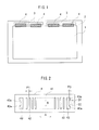
- FIG. 1 is a plain view showing a configuration of a liquid crystal display apparatus when an external housing is removed and chip mounted circuit substrates are mounted on a liquid crystal display panel;
- FIG. 2 is a plain view showing a configuration of the chip mounted circuit substrate in accordance with an embodiment of the present invention
- FIG. 3 is a view showing a method to mount the chip mounted circuit substrate on the liquid crystal display panel in a state before thermo-compression bonding process
- FIG. 4A is a view showing a state that the chip mounted circuit substrate is positioned on the liquid crystal display panel.
- FIG. 4B is a view showing a state that the chip mounted circuit substrate is fixed on the liquid crystal display panel by thermo-compression bonding.
- FIG. 1 shows a state of a liquid crystal display apparatus where an external housing is removed.
- an external frame 2 encloses a liquid crystal display panel 1 and circuit boards 3 are held on the external frame 2.
- a plurality of chip mounted circuit substrates (or chip on flexible printed circuit substrates: hereinafter abbreviated as COF) 4 are used to connect the circuit board 3 and transparent electrodes such as TFT (thin film transistor) formed on a surface of the liquid crystal display panel 1.
- COF chip mounted circuit substrates
- FIG. 2 shows a constitution of the COF 4 in accordance with this embodiment.
- the COF 4 comprises a base film 41, wiring electrodes 42 which are arranged on the base film 41 at a first pitch P1 in a first direction (A-direction), and two of first positioning marks 43 which are formed at positions near to both sides of the arrangement of the wiring electrodes 42 in the first direction.
- Each wiring electrode 42 has constant dimensions (width and length) in the first direction and a second direction (B-direction) perpendicular to the first direction (A-direction).
- the first pitch P1 before installing the COF 4 on the liquid crystal display panel 1 by the thermo-compression bonding is selected to be narrower (or smaller) than a second pitch P2 (see FIG. 4B ) which is the radical pitch of the wiring electrodes 42 after installing the COF 4 on the liquid crystal display panel 1 in consideration of the expansion of the base film 41 in the first direction.
- the wiring electrodes 42 and the transparent electrodes 12 which will be described later are schematically illustrated for showing connecting portion of them, and illustration of detailed shapes of them in the second direction is omitted.
- the first positioning marks 43 on the COF are dummy electrodes which are not used as wiring electrodes.
- Each first positioning mark 43 has stepped portions 43a in outer end portion of the first positioning mark 43 opposite to the arrangement of the wiring electrodes 42 in the first direction (A-direction).
- the stepped portions 43a are formed so that distances D1, D2 in the second direction (B-direction) between opposing two sides of the stepped portions 43a in parallel with the first direction become shorter in phase.
- each side of the stepped portions 43a in parallel with the first direction has a length P3.
- each step of the stepped portions 43a is formed at a third pitch P3 in the first direction (and in the second direction, if possible). In the example shown in FIG.
- both outer sides of the first positioning mark 43 in the second direction are formed to be straight lines, and inner sides are formed to have stepped shapes.
- the stepped portions 43a is sufficient to serve as a kind of scale, it is possible to form the first positioning marks 43 may be formed in converse manner that the stepped portions 43a are formed on outer sides of the first positioning marks 43 in the second direction, for example.
- FIG. 3 shows a state before installing the COF 4 to the liquid crystal panel 1 by the thermo-compression bonding.
- transparent electrodes 12 such as TFT and second positioning marks 13 are formed.
- the liquid crystal display panel 1 hardly expands, and relative positions of the second positioning marks 13 to the transparent electrodes 12 on the liquid crystal display panel 1 are hardly displaced.
- the second positioning marks 13 can be used as a part of electrodes of the liquid crystal display panel 1. Since widths of the transparent electrodes 12 in the first direction (A-direction) are not necessarily constant, it is possible to vary the width of each transparent electrode 12 corresponding to value of electric current flowing into the transparent electrode 12.
- a plurality (not limited to two) of the wiring electrodes 42 of the COF 4 may be connected to a wide transparent electrode 12, for example.
- FIG. 4A shows a state that the COF 4 is positioned on the liquid crystal display panel 1
- FIG. 4B shows a state that the COF 4 is installed on the liquid crystal display panel 1 by the thermo-compression bonding.
- the outline of the liquid crystal display panel 1 is omitted from the illustration of FIGS. 4A and 4B .
- the first positioning marks 43 are formed so that a part of each the first positioning mark 43 overlaps the second positioning mark 13 formed on the liquid crystal display panel 1 and protrudes outward from the second positioning mark 13 in the first direction (A-direction).
- the stepped portion 43a Since the portion of the first positioning mark 43 protruding from the second positioning mark 13, that is, the stepped portion 43a is formed to be the steeped shapes, it is possible to use the stepped portion 43a as a scale. A worker can dispose the COF 4 on the liquid crystal display panel 1 using the scale so that quantities of protrusions of the first positioning marks 43 from the second positioning marks 13 in both sides in the first direction (A-direction) become substantially equal by manual labor with visual observation. In addition, positioning precision of the COF 4 on the liquid crystal display panel 1 in the second direction (B-direction) may be a little rough in comparison with that in the first direction (A-direction).
- thermo-compression bonding is performed from a central region of the COF 4 to both peripheral regions in the first direction (A-direction). Then, the base film 41 of the COF 4 expands in the first direction (A-direction) and in the second direction (B-direction) as shown in FIG. 4B , and the pitch of the arrangement of the wiring electrodes 42 of the COF 4 is expanded from the first pitch P1 to the second pitch P2 responding to the expansion of the base film 41, as shown in FIG. 4B . Consequently, one or more wiring electrodes 42 of the COF 4 is/are connected to each transparent electrode 12 of the liquid crystal display panel 1, as shown in FIG. 4B . Although the positions of the first positioning marks 43 of the COF 4 are displaced due to the expansion of the base film 41, the first positioning marks 43 are dummy electrodes which are not used as the wiring electrodes, so that the existence of the first positioning marks 43 causes no problem.
- the worker can easily position the COF 4 on the liquid crystal display panel 1 before the thermo-compression bonding by disposing the COF 4 on the liquid crystal display panel 1 so that quantities of protrusions of the first positioning marks 43 from the second positioning marks in both sides in the first direction (A-direction) become substantially equal by manual labor with visual observation.
- the portion of the first positioning mark 43 protruding from the second positioning mark 13 is formed to be stepped shapes, the stepped shaped portion can be used as a scale, and thus, the worker can easily make the quantities of protrusions of the first positioning marks 43 from the second positioning marks 13 in both sides in the first direction (A-direction) substantially equal.
- the first pitch P1 of the arrangement of the wiring electrodes 42 of the COF 4 is made narrower/smaller that the second pitch P2 after installing the COF 4 on the liquid crystal display panel 1 in consideration of expansion of the base film 41 due to the thermo-compression bonding, so that the wiring electrodes 42 can be precisely connected to the transparent electrodes 12 of the liquid crystal display panel 1.
Landscapes
- Engineering & Computer Science (AREA)
- Manufacturing & Machinery (AREA)
- Microelectronics & Electronic Packaging (AREA)
- Liquid Crystal (AREA)
- Devices For Indicating Variable Information By Combining Individual Elements (AREA)
- Structure Of Printed Boards (AREA)
- Combinations Of Printed Boards (AREA)
Abstract
A chip mounted circuit substrate (COF) 4 to be installed on a liquid crystal display panel 1 comprises an arrangement wiring electrodes 42 formed on a base film 41 at a first pitch P1 in a first direction (A-direction) and two of first positioning marks 43 formed at both sides of the arrangement of the wiring electrodes 43 in the first direction. Before installing the COF 4 on the liquid crystal display panel 1 by thermo-compression bonding, the first pitch P1 of the wiring electrodes 42 is selected to be narrower than a second pitch P2 after performing the thermo-compression bonding in consideration with expansion of the base film 41 in the first direction. In addition, a part of each the first positioning mark 43 overlaps a second positioning mark 12 formed on the liquid crystal display panel 1 and protrudes outward from the second positioning mark 12 in the first direction.
Description
- The present invention relates to an assembling method of a chip mounted wiring substrate to a liquid crystal display panel in a liquid crystal display apparatus and a chip mounted wiring substrate suitable for the method.
- In late years, a chip mounted wiring substrate (or chip-on flexible printed circuit substrate: hereinafter it is abbreviated as COF), which enables the miniaturization of wiring pitch responding to the miniaturization of the pitch of a driver IC, is used for assembling of the liquid crystal display apparatuses. The COF has a flexible printed circuit substrate (FPC) that connection wirings are formed on a base film and a driver IC is mounted on the FPC.
- In case of manufacturing the liquid crystal display apparatuses in a factory in large quantities, as described in the prior arts
JP 3-231228A JP 9-218420A JP 2007-123344A - However, when the COF is dismounted from the liquid crystal display panel to repair the liquid crystal display apparatus, the COF must be attached to the liquid crystal display panel again by manual labor of a worker. Specifically, the worker must locate the COF on the liquid crystal display panel so that the positioning marks of the COF are disposed just above the positioning marks of the liquid crystal display panel and performs the thermo-compression bonding with keeping the posture. However, it is really very difficult and takes long time to perform the thermo-compression bonding by manual labor from a practical standpoint. In addition, although the wiring electrodes of the COF are arranged to have equal width and space, the cell electrodes of the liquid crystal display panel are not necessarily arranged to have equal width and space. Thus, if the width of the cell electrodes of the liquid crystal display panel is wider than that of the wiring electrodes of the COF, when the wiring electrodes formed on the COF are located above the cell electrodes of the liquid crystal display panel, the wiring electrodes may be blinded by the cell electrodes. Consequently, it is difficult to judge whether the COF is precisely positioned on the liquid crystal display panel or not by visual check.
- In addition,
JP 2005-284004A - The present invention is conceived to solve the above mentioned problems and purposed to provide an assembling method of a liquid crystal display apparatus and a chip mounted wiring substrate suitable for the method, which enable to connect the COF and the liquid crystal display panel precisely and easily by manual labor.
- An assembling method of a liquid crystal display apparatus to install a chip mounted circuit substrate on a liquid crystal display panel in accordance with an aspect of the present invention has steps of:
- forming the chip mounted circuit substrate to comprise a plurality of wiring electrodes arranged on a base film at a first pitch in a first direction and two of first positioning marks formed at both sides of an arrangement of the wiring electrodes in the first direction, the first pitch of the arrangement of the wiring electrodes is selected to be narrower than a second pitch of the arrangement of the wiring electrodes after installing the chip mounted circuit substrate on the liquid crystal display panel by thermo-compression bonding in consideration with expansion of the base film in the first direction due to the thermo-compression bonding, and the first positioning marks are formed so that a part of each the first positioning mark overlaps a second positioning mark formed on the liquid crystal display panel and protrudes outward from the second positioning mark in the first direction, in a state before installing the chip mounted circuit substrate on the liquid crystal display panel by thermo-compression bonding;
- disposing the chip mounted circuit substrate on the liquid crystal display panel so that quantities of protrusions of the first positioning marks from the second positioning marks in both sides in the first direction become substantially equal when the chip mounted circuit substrate is installed on the liquid crystal display panel by the thermo-compression bonding; and
- performing the thermo-compression bonding from a central region to outer peripheral regions of the chip mounted circuit substrate in the first direction.
- A chip mounted circuit substrate in accordance with an aspect of the invention comprises:
- a plurality of wiring electrodes arranged on a base film at a first pitch in a first direction; and
- two of first positioning marks formed at both sides of an arrangement of the wiring electrodes in the first direction, wherein
- in a state before installing the chip mounted circuit substrate on a liquid crystal display panel by thermo-compression bonding,
- the first pitch of the arrangement of the wiring electrodes is selected to be narrower than a second pitch of the arrangement of the wiring electrodes after installing the chip mounted circuit substrate on the liquid crystal display panel by thermo-compression bonding in consideration with expansion of the base film in the first direction due to the thermo-compression bonding, and
- the first positioning marks are formed so that a part of each the first positioning mark overlaps a second positioning mark formed on the liquid crystal display panel and protrudes outward from the second positioning mark in the first direction.
- According to such configurations, since two of the first positioning marks of the chip mounted circuit substrate are formed larger to protrude from the second positioning marks of the liquid crystal display panel, the worker can easily position the chip mounted circuit substrate on the liquid crystal display panel before the thermo-compression bonding by disposing the chip mounted circuit substrate on the liquid crystal display panel so that quantities of protrusions of the first positioning marks from the second positioning marks in both sides in the first direction become substantially equal by manual labor with visual observation. Moreover, the first pitch of the arrangement of the wiring electrodes of the chip mounted circuit substrate is made narrower/smaller than the second pitch after installing the chip mounted circuit substrate on the liquid crystal display panel in consideration of expansion of the base film due to the thermo-compression bonding, so that the wiring electrodes can be precisely connected to the transparent electrodes of the liquid crystal display panel.
- While the novel features of the present invention are set forth in the appended claims, the present invention will be better understood from the following detailed description taken in conjunction with the drawings.
- The present invention will be described hereinafter with reference to the annexed drawings. It is to be noted that all the drawings are shown for the purpose of illustrating the technical concept of the present invention or embodiments thereof, wherein:
-
FIG. 1 is a plain view showing a configuration of a liquid crystal display apparatus when an external housing is removed and chip mounted circuit substrates are mounted on a liquid crystal display panel; -
FIG. 2 is a plain view showing a configuration of the chip mounted circuit substrate in accordance with an embodiment of the present invention; -
FIG. 3 is a view showing a method to mount the chip mounted circuit substrate on the liquid crystal display panel in a state before thermo-compression bonding process; -
FIG. 4A is a view showing a state that the chip mounted circuit substrate is positioned on the liquid crystal display panel; and -
FIG. 4B is a view showing a state that the chip mounted circuit substrate is fixed on the liquid crystal display panel by thermo-compression bonding. - An assembling method of a liquid crystal display apparatus and a chip mounted wiring substrate suitable for the method in accordance with an embodiment of the present invention is described with reference to the figures.
FIG. 1 shows a state of a liquid crystal display apparatus where an external housing is removed. As can be seen fromFIG. 1 , anexternal frame 2 encloses a liquidcrystal display panel 1 andcircuit boards 3 are held on theexternal frame 2. A plurality of chip mounted circuit substrates (or chip on flexible printed circuit substrates: hereinafter abbreviated as COF) 4 are used to connect thecircuit board 3 and transparent electrodes such as TFT (thin film transistor) formed on a surface of the liquidcrystal display panel 1. -
FIG. 2 shows a constitution of theCOF 4 in accordance with this embodiment. As shown inFIG. 2 , theCOF 4 comprises abase film 41,wiring electrodes 42 which are arranged on thebase film 41 at a first pitch P1 in a first direction (A-direction), and two offirst positioning marks 43 which are formed at positions near to both sides of the arrangement of thewiring electrodes 42 in the first direction. Eachwiring electrode 42 has constant dimensions (width and length) in the first direction and a second direction (B-direction) perpendicular to the first direction (A-direction). Since thebase film 41 expands in the first direction and in the second direction while thermo-compression bonding is performed, the first pitch P1 before installing theCOF 4 on the liquidcrystal display panel 1 by the thermo-compression bonding is selected to be narrower (or smaller) than a second pitch P2 (seeFIG. 4B ) which is the radical pitch of thewiring electrodes 42 after installing theCOF 4 on the liquidcrystal display panel 1 in consideration of the expansion of thebase film 41 in the first direction. In addition, thewiring electrodes 42 and thetransparent electrodes 12 which will be described later are schematically illustrated for showing connecting portion of them, and illustration of detailed shapes of them in the second direction is omitted. - The first positioning marks 43 on the COF are dummy electrodes which are not used as wiring electrodes. Each
first positioning mark 43 has steppedportions 43a in outer end portion of thefirst positioning mark 43 opposite to the arrangement of thewiring electrodes 42 in the first direction (A-direction). Thestepped portions 43a are formed so that distances D1, D2 in the second direction (B-direction) between opposing two sides of thestepped portions 43a in parallel with the first direction become shorter in phase. In addition, each side of thestepped portions 43a in parallel with the first direction has a length P3. In other words, each step of thestepped portions 43a is formed at a third pitch P3 in the first direction (and in the second direction, if possible). In the example shown inFIG. 2 , both outer sides of thefirst positioning mark 43 in the second direction (B-direction) are formed to be straight lines, and inner sides are formed to have stepped shapes. However, since the steppedportions 43a is sufficient to serve as a kind of scale, it is possible to form the first positioning marks 43 may be formed in converse manner that the steppedportions 43a are formed on outer sides of the first positioning marks 43 in the second direction, for example. -
FIG. 3 shows a state before installing theCOF 4 to theliquid crystal panel 1 by the thermo-compression bonding. On the surface of the liquidcrystal display panel 1,transparent electrodes 12 such as TFT and second positioning marks 13 are formed. In addition, when installing theCOF 4 on the liquidcrystal display panel 1 by the thermo-compression bonding, the liquidcrystal display panel 1 hardly expands, and relative positions of the second positioning marks 13 to thetransparent electrodes 12 on the liquidcrystal display panel 1 are hardly displaced. Thus, the second positioning marks 13 can be used as a part of electrodes of the liquidcrystal display panel 1. Since widths of thetransparent electrodes 12 in the first direction (A-direction) are not necessarily constant, it is possible to vary the width of eachtransparent electrode 12 corresponding to value of electric current flowing into thetransparent electrode 12. A plurality (not limited to two) of thewiring electrodes 42 of theCOF 4 may be connected to a widetransparent electrode 12, for example. -
FIG. 4A shows a state that theCOF 4 is positioned on the liquidcrystal display panel 1, andFIG. 4B shows a state that theCOF 4 is installed on the liquidcrystal display panel 1 by the thermo-compression bonding. The outline of the liquidcrystal display panel 1 is omitted from the illustration ofFIGS. 4A and 4B . In the state before installing theCOF 4 on the liquidcrystal display panel 1 by the thermo-compression bonding as shown inFIG. 4A , the first positioning marks 43 are formed so that a part of each thefirst positioning mark 43 overlaps thesecond positioning mark 13 formed on the liquidcrystal display panel 1 and protrudes outward from thesecond positioning mark 13 in the first direction (A-direction).
Since the portion of thefirst positioning mark 43 protruding from thesecond positioning mark 13, that is, the steppedportion 43a is formed to be the steeped shapes, it is possible to use the steppedportion 43a as a scale. A worker can dispose theCOF 4 on the liquidcrystal display panel 1 using the scale so that quantities of protrusions of the first positioning marks 43 from the second positioning marks 13 in both sides in the first direction (A-direction) become substantially equal by manual labor with visual observation. In addition, positioning precision of theCOF 4 on the liquidcrystal display panel 1 in the second direction (B-direction) may be a little rough in comparison with that in the first direction (A-direction). - In the state shown in
FIG. 4A , the thermo-compression bonding is performed from a central region of theCOF 4 to both peripheral regions in the first direction (A-direction). Then, thebase film 41 of theCOF 4 expands in the first direction (A-direction) and in the second direction (B-direction) as shown inFIG. 4B , and the pitch of the arrangement of thewiring electrodes 42 of theCOF 4 is expanded from the first pitch P1 to the second pitch P2 responding to the expansion of thebase film 41, as shown inFIG. 4B . Consequently, one ormore wiring electrodes 42 of theCOF 4 is/are connected to eachtransparent electrode 12 of the liquidcrystal display panel 1, as shown inFIG. 4B . Although the positions of the first positioning marks 43 of theCOF 4 are displaced due to the expansion of thebase film 41, the first positioning marks 43 are dummy electrodes which are not used as the wiring electrodes, so that the existence of the first positioning marks 43 causes no problem. - As mentioned above, according to the present invention, since two of the first positioning marks 43 of the
COF 4 are formed larger to protrude from the second positioning marks 12 of the liquidcrystal display panel 1, the worker can easily position theCOF 4 on the liquidcrystal display panel 1 before the thermo-compression bonding by disposing theCOF 4 on the liquidcrystal display panel 1 so that quantities of protrusions of the first positioning marks 43 from the second positioning marks in both sides in the first direction (A-direction) become substantially equal by manual labor with visual observation. In addition, since the portion of thefirst positioning mark 43 protruding from thesecond positioning mark 13 is formed to be stepped shapes, the stepped shaped portion can be used as a scale, and thus, the worker can easily make the quantities of protrusions of the first positioning marks 43 from the second positioning marks 13 in both sides in the first direction (A-direction) substantially equal. Moreover, the first pitch P1 of the arrangement of thewiring electrodes 42 of theCOF 4 is made narrower/smaller that the second pitch P2 after installing theCOF 4 on the liquidcrystal display panel 1 in consideration of expansion of thebase film 41 due to the thermo-compression bonding, so that thewiring electrodes 42 can be precisely connected to thetransparent electrodes 12 of the liquidcrystal display panel 1. - This application is based on Japanese patent application
2009-289276 filed December 21, 2009 - Although the present invention has been fully described by way of example with reference to the accompanying drawings, it is to be understood that various changes and modifications will be apparent to those skilled in the art. Therefore, unless otherwise such changes and modifications depart from the scope of the present invention, they should be construed as being included therein.
Claims (4)
- An assembling method of a liquid crystal display apparatus to install a chip mounted circuit substrate (4) on a liquid crystal display panel (1), having steps of:forming the chip mounted circuit substrate (4) to comprise a plurality of wiring electrodes (42) arranged on a base film (41) at a first pitch (P1) in a first direction (A-direction) and two of first positioning marks (43) formed at both sides of an arrangement of the wiring electrodes (42) in the first direction (A-direction), the first pitch (P1) of the arrangement of the wiring electrodes (42) is selected to be narrower than a second pitch (P2) of the arrangement of the wiring electrodes (42) after installing the chip mounted circuit substrate (4) on the liquid crystal display panel (1) by thermo-compression bonding (FIG. 4B) in consideration with expansion of the base film (41) in the first direction (A-direction) due to the thermo-compression bonding, and the first positioning marks (43) are formed so that a part (43a) of each the first positioning mark (43) overlaps a second positioning mark (13) formed on the liquid crystal display panel (1) and protrudes outward from the second positioning mark (13) in the first direction (A-direction), in a state before installing the chip mounted circuit substrate (4) on the liquid crystal display panel (1) by thermo-compression bonding (FIGS. 2 and 4A);disposing the chip mounted circuit substrate (4) on the liquid crystal display panel (1) so that quantities of protrusions of the first positioning marks (43) from the second positioning marks (13) in both sides in the first direction (A-direction) becomes substantially equal (FIG. 4A) when the chip mounted circuit substrate (4) is installed on the liquid crystal display panel (1) by the thermo-compression bonding; andperforming the thermo-compression bonding from a central region to outer peripheral regions of the chip mounted circuit substrate (4) in the first direction (A-direction) (FIG. 4B).
- The assembling method of the liquid crystal display apparatus in accordance with claim 1, wherein
the portions of the first positioning marks (43) protruding from the second positioning marks (13) are formed to have stepped shapes (43a) so that distances (D1, D2) in a second direction (B-direction) perpendicular to the first direction (A-direction) between opposing two sides of the stepped shapes (43a) in parallel with the first direction (A-direction) become shorter in phase and each step of the stepped shapes (43a) is formed at a third pitch (P3) in the first direction (A-direction). - A chip mounted circuit substrate (4) comprising:a plurality of wiring electrodes (42) arranged on a base film (41) at a first pitch (P1) in a first direction (A-direction); andtwo of first positioning marks (43) formed at both sides of an arrangement of the wiring electrodes (42) in the first direction (A-direction), whereinin a state before installing the chip mounted circuit substrate (4) on a liquid crystal display panel (1) by thermo-compression bonding (FIGS. 2 and 4A),the first pitch (P1) of the arrangement of the wiring electrodes (42) is selected to be narrower than a second pitch (P2) of the arrangement of the wiring electrodes (42) after installing the chip mounted circuit substrate (4) on the liquid crystal display panel (1) by thermo-compression bonding (FIG. 4B) in consideration with expansion of the base film (41) in the first direction (A-direction) due to the thermo-compression bonding, andthe first positioning marks (43) are formed so that a part (43a) of each the first positioning mark (43) overlaps a second positioning mark (13) formed on the liquid crystal display panel (1) and protrudes outward from the second positioning mark (13) in the first direction (A-direction).
- The chip mounted circuit substrate in accordance with claim 3, wherein
the portions of the first positioning marks (43) protruding from the second positioning marks (13) are formed to have stepped shapes (43a) so that distances (D1, D2) in a second direction (B-direction) perpendicular to the first direction (A-direction) between opposing two sides of the stepped shapes (43a) in parallel with the first direction (A-direction) become shorter in phase and each step of the stepped shapes (43a) is formed at a third pitch (P3) in the first direction (A-direction).
Applications Claiming Priority (1)
| Application Number | Priority Date | Filing Date | Title |
|---|---|---|---|
| JP2009289276A JP5526756B2 (en) | 2009-12-21 | 2009-12-21 | Mounting method of liquid crystal display device and chip mounting wiring board suitable for the same |
Publications (1)
| Publication Number | Publication Date |
|---|---|
| EP2337434A1 true EP2337434A1 (en) | 2011-06-22 |
Family
ID=43736280
Family Applications (1)
| Application Number | Title | Priority Date | Filing Date |
|---|---|---|---|
| EP10194433A Withdrawn EP2337434A1 (en) | 2009-12-21 | 2010-12-10 | Assembling method of a liquid crystal display apparatus and a chip mounted wiring substrate suitable for the method |
Country Status (3)
| Country | Link |
|---|---|
| US (1) | US8615871B2 (en) |
| EP (1) | EP2337434A1 (en) |
| JP (1) | JP5526756B2 (en) |
Cited By (1)
| Publication number | Priority date | Publication date | Assignee | Title |
|---|---|---|---|---|
| CN110265445A (en) * | 2019-06-21 | 2019-09-20 | 京东方科技集团股份有限公司 | Display device and electronic device |
Families Citing this family (3)
| Publication number | Priority date | Publication date | Assignee | Title |
|---|---|---|---|---|
| CN102495484B (en) * | 2011-12-02 | 2015-12-16 | 深圳市华星光电技术有限公司 | A kind of liquid crystal indicator and preparation method thereof |
| KR102330882B1 (en) | 2014-10-13 | 2021-11-25 | 삼성디스플레이 주식회사 | Display device |
| JP2019139073A (en) * | 2018-02-09 | 2019-08-22 | 株式会社ジャパンディスプレイ | Display device and wiring board |
Citations (9)
| Publication number | Priority date | Publication date | Assignee | Title |
|---|---|---|---|---|
| JPH03231228A (en) | 1990-02-06 | 1991-10-15 | Seiko Epson Corp | Liquid crystal display device |
| JPH0521515A (en) * | 1991-07-15 | 1993-01-29 | Seiko Epson Corp | Liquid crystal display device and manufacturing method thereof |
| JPH09218420A (en) | 1997-02-06 | 1997-08-19 | Seiko Epson Corp | Manufacturing method of liquid crystal display device |
| JP2005284004A (en) | 2004-03-30 | 2005-10-13 | Sharp Corp | Display panel mounting structure and mounting method |
| JP2007123344A (en) | 2005-10-25 | 2007-05-17 | Toshiba Matsushita Display Technology Co Ltd | Liquid crystal display device |
| US20070246836A1 (en) * | 2006-04-19 | 2007-10-25 | Ichiyama Iwane | Electric terminal device and method of connecting the same |
| US20080030666A1 (en) * | 2006-08-04 | 2008-02-07 | Hideaki Abe | Display device |
| JP2009289276A (en) | 2009-08-27 | 2009-12-10 | Toshiba Tec Corp | Commodity sales data processor |
| EP2237101A1 (en) * | 2009-04-01 | 2010-10-06 | Funai Electric Co., Ltd. | Liquid crystal module |
Family Cites Families (9)
| Publication number | Priority date | Publication date | Assignee | Title |
|---|---|---|---|---|
| JPS61123868A (en) * | 1984-11-21 | 1986-06-11 | キヤノン株式会社 | Positioning securing method for panel substrate |
| US5386309A (en) * | 1990-12-20 | 1995-01-31 | Goldstar Co., Ltd. | Liquid crystal display module with positioning marks on circuit substrate and heat seal |
| TW347479B (en) * | 1994-12-15 | 1998-12-11 | Sharp Kk | Liquid crystal display panel and liquid crystal display apparatus |
| JP3231228B2 (en) | 1995-10-24 | 2001-11-19 | オルガノ株式会社 | Regeneration method of ion exchange resin tower |
| US6266119B1 (en) * | 1998-01-13 | 2001-07-24 | Canon Kabushiki Kaisha | Liquid crystal apparatus and production process thereof |
| JP4651886B2 (en) * | 2001-09-14 | 2011-03-16 | 東北パイオニア株式会社 | Electronic device and method for manufacturing electronic device |
| US6867841B2 (en) * | 2001-10-31 | 2005-03-15 | Hitachi, Ltd. | Method for manufacturing liquid crystal display panels |
| JP4064808B2 (en) * | 2001-12-25 | 2008-03-19 | 東芝松下ディスプレイテクノロジー株式会社 | Thermocompression bonding apparatus and thermocompression bonding method |
| JP2005251930A (en) * | 2004-03-03 | 2005-09-15 | Seiko Epson Corp | Mounting structure, inspection method, electro-optical device manufacturing method, electro-optical device, and electronic apparatus |
-
2009
- 2009-12-21 JP JP2009289276A patent/JP5526756B2/en not_active Expired - Fee Related
-
2010
- 2010-12-10 EP EP10194433A patent/EP2337434A1/en not_active Withdrawn
- 2010-12-14 US US12/967,427 patent/US8615871B2/en not_active Expired - Fee Related
Patent Citations (9)
| Publication number | Priority date | Publication date | Assignee | Title |
|---|---|---|---|---|
| JPH03231228A (en) | 1990-02-06 | 1991-10-15 | Seiko Epson Corp | Liquid crystal display device |
| JPH0521515A (en) * | 1991-07-15 | 1993-01-29 | Seiko Epson Corp | Liquid crystal display device and manufacturing method thereof |
| JPH09218420A (en) | 1997-02-06 | 1997-08-19 | Seiko Epson Corp | Manufacturing method of liquid crystal display device |
| JP2005284004A (en) | 2004-03-30 | 2005-10-13 | Sharp Corp | Display panel mounting structure and mounting method |
| JP2007123344A (en) | 2005-10-25 | 2007-05-17 | Toshiba Matsushita Display Technology Co Ltd | Liquid crystal display device |
| US20070246836A1 (en) * | 2006-04-19 | 2007-10-25 | Ichiyama Iwane | Electric terminal device and method of connecting the same |
| US20080030666A1 (en) * | 2006-08-04 | 2008-02-07 | Hideaki Abe | Display device |
| EP2237101A1 (en) * | 2009-04-01 | 2010-10-06 | Funai Electric Co., Ltd. | Liquid crystal module |
| JP2009289276A (en) | 2009-08-27 | 2009-12-10 | Toshiba Tec Corp | Commodity sales data processor |
Cited By (3)
| Publication number | Priority date | Publication date | Assignee | Title |
|---|---|---|---|---|
| CN110265445A (en) * | 2019-06-21 | 2019-09-20 | 京东方科技集团股份有限公司 | Display device and electronic device |
| CN110265445B (en) * | 2019-06-21 | 2021-09-21 | 京东方科技集团股份有限公司 | Display device and electronic device |
| US11329038B2 (en) | 2019-06-21 | 2022-05-10 | Boe Technology Group Co., Ltd. | Display device and electronic equipment |
Also Published As
| Publication number | Publication date |
|---|---|
| JP5526756B2 (en) | 2014-06-18 |
| JP2011128530A (en) | 2011-06-30 |
| US20110146067A1 (en) | 2011-06-23 |
| US8615871B2 (en) | 2013-12-31 |
Similar Documents
| Publication | Publication Date | Title |
|---|---|---|
| CN101075037B (en) | Display device | |
| JPWO2000054098A1 (en) | Liquid crystal display device and inspection method thereof | |
| KR20070110202A (en) | Tape Carrier and Semiconductor Device and Semiconductor Module Device | |
| US7339646B2 (en) | Connection structures of wiring board and connection structure of liquid crystal display panel | |
| US8615871B2 (en) | Chip mounted wiring substrate | |
| US7656089B2 (en) | Tape carrier package on reel and plasma display device using the same | |
| JP7148310B2 (en) | Flexible substrate and display device | |
| US6559522B1 (en) | Tape carrier package and an LCD module using the same | |
| KR101274939B1 (en) | Drive-IC and LC module | |
| CN100461984C (en) | Circuit Assembly Structure | |
| EP2237101A1 (en) | Liquid crystal module | |
| EP2128685A1 (en) | Liquid crystal display apparatus and method for manufacturing liquid crystal display apparatus | |
| US6867482B2 (en) | Tape carrier type semiconductor device, method for manufacturing the same, and flexible substrate | |
| US20060001820A1 (en) | Liquid crystal module | |
| KR100320309B1 (en) | Liquid-crystal-panel driver ic package and liquid crystal panel module | |
| JP2016207792A (en) | Flexible printed board and image display device | |
| JP2008130803A (en) | Board device and substrate | |
| JP2018098448A (en) | Manufacturing method of flexible printed circuit board | |
| KR20160093445A (en) | Display device having flexible printed circuit | |
| JP2003289087A (en) | Wiring board, semiconductor device and manufacturing method thereof, panel module, and electronic device | |
| JP4413637B2 (en) | Display device | |
| KR100589459B1 (en) | Tape carrier package and its manufacturing method_ | |
| KR200234998Y1 (en) | Plasma Display Panel Device | |
| JP2008010712A (en) | Flexible substrate | |
| JP2007322732A (en) | Display device |
Legal Events
| Date | Code | Title | Description |
|---|---|---|---|
| PUAI | Public reference made under article 153(3) epc to a published international application that has entered the european phase |
Free format text: ORIGINAL CODE: 0009012 |
|
| AK | Designated contracting states |
Kind code of ref document: A1 Designated state(s): AL AT BE BG CH CY CZ DE DK EE ES FI FR GB GR HR HU IE IS IT LI LT LU LV MC MK MT NL NO PL PT RO RS SE SI SK SM TR |
|
| AX | Request for extension of the european patent |
Extension state: BA ME |
|
| 17P | Request for examination filed |
Effective date: 20111212 |
|
| 17Q | First examination report despatched |
Effective date: 20141022 |
|
| STAA | Information on the status of an ep patent application or granted ep patent |
Free format text: STATUS: THE APPLICATION IS DEEMED TO BE WITHDRAWN |
|
| 18D | Application deemed to be withdrawn |
Effective date: 20150503 |