EP2336817B2 - Dispositif destiné à l'analyse d'un échantillon comprenant un microscope - Google Patents
Dispositif destiné à l'analyse d'un échantillon comprenant un microscope Download PDFInfo
- Publication number
- EP2336817B2 EP2336817B2 EP10193888.4A EP10193888A EP2336817B2 EP 2336817 B2 EP2336817 B2 EP 2336817B2 EP 10193888 A EP10193888 A EP 10193888A EP 2336817 B2 EP2336817 B2 EP 2336817B2
- Authority
- EP
- European Patent Office
- Prior art keywords
- semiconductor elements
- sample
- light beam
- detection
- detector
- Prior art date
- Legal status (The legal status is an assumption and is not a legal conclusion. Google has not performed a legal analysis and makes no representation as to the accuracy of the status listed.)
- Active
Links
- 239000004065 semiconductor Substances 0.000 claims description 60
- 238000001514 detection method Methods 0.000 claims description 36
- 238000011156 evaluation Methods 0.000 claims description 7
- 238000005286 illumination Methods 0.000 claims description 7
- 238000001816 cooling Methods 0.000 claims description 5
- 230000001681 protective effect Effects 0.000 claims description 4
- 230000015556 catabolic process Effects 0.000 claims description 2
- 239000007788 liquid Substances 0.000 claims description 2
- 238000011144 upstream manufacturing Methods 0.000 claims 1
- 230000000694 effects Effects 0.000 description 6
- 238000003491 array Methods 0.000 description 3
- 238000001444 catalytic combustion detection Methods 0.000 description 3
- 238000005516 engineering process Methods 0.000 description 3
- 238000002060 fluorescence correlation spectroscopy Methods 0.000 description 3
- 230000035945 sensitivity Effects 0.000 description 3
- 238000000098 azimuthal photoelectron diffraction Methods 0.000 description 2
- 238000010586 diagram Methods 0.000 description 2
- 238000002376 fluorescence recovery after photobleaching Methods 0.000 description 2
- 238000002866 fluorescence resonance energy transfer Methods 0.000 description 2
- 238000005259 measurement Methods 0.000 description 2
- 238000006862 quantum yield reaction Methods 0.000 description 2
- 230000003595 spectral effect Effects 0.000 description 2
- 206010036618 Premenstrual syndrome Diseases 0.000 description 1
- 230000005540 biological transmission Effects 0.000 description 1
- 230000015572 biosynthetic process Effects 0.000 description 1
- 238000010276 construction Methods 0.000 description 1
- 230000008878 coupling Effects 0.000 description 1
- 238000010168 coupling process Methods 0.000 description 1
- 238000005859 coupling reaction Methods 0.000 description 1
- 230000001419 dependent effect Effects 0.000 description 1
- 230000002349 favourable effect Effects 0.000 description 1
- 238000003384 imaging method Methods 0.000 description 1
- 238000000034 method Methods 0.000 description 1
- 238000000386 microscopy Methods 0.000 description 1
- 238000012545 processing Methods 0.000 description 1
- 230000002123 temporal effect Effects 0.000 description 1
Images
Classifications
-
- G—PHYSICS
- G02—OPTICS
- G02B—OPTICAL ELEMENTS, SYSTEMS OR APPARATUS
- G02B21/00—Microscopes
- G02B21/0004—Microscopes specially adapted for specific applications
- G02B21/002—Scanning microscopes
- G02B21/0024—Confocal scanning microscopes (CSOMs) or confocal "macroscopes"; Accessories which are not restricted to use with CSOMs, e.g. sample holders
- G02B21/008—Details of detection or image processing, including general computer control
Definitions
- the invention relates to a device for examining a sample, comprising a microscope with a light source, a scanning unit and a detector.
- the light source produces an illuminating light beam.
- the scanning unit deflects the illuminating light beam directed onto the sample via an objective and thereby moves a focus area of the illuminating light beam within a predetermined scanning field on or in the sample.
- the detector detects a detection light beam emanating from the sample and not deflected by the scanning unit.
- a selected punctiform or line-shaped area of the sample is optically scanned at a predetermined point in time.
- a focusing optics, in particular a lens, of the microscope focuses the illuminating light beam on the selected area of the sample and detects the portion of the light that is reflected from the selected area, for example due to fluorescence effects in the sample.
- the image data obtained is saved. Further areas in the form of points or lines are then examined, which preferably border one another and form a line or an area, for example. In this way, a large area of the sample can be optically scanned point by point and line by line.
- NDDs Non-Descanned-Detector
- photomultipliers or EMCCDs electron multiplying CCD are used as photosensitive components. These are preferred over other photosensitive components because their light-sensitive area can be made relatively large, which is necessary because the scanning movement of the illuminating light beam also causes the detection light beam to move at least slightly on the photosensitive surface of the detector and because this requires a minimal size of the light-sensitive Area of the photosensitive component of typically 3mm x 3mm is required in order to be able to direct light from all scan positions onto the light-sensitive area.
- the detection light is, in particular, fluorescent light emitted by the sample.
- avalanche photodiodes To detect the detection beams, which are fed back via the scanner, avalanche photodiodes (APDs for short) are used as light detectors, among others. These are much more sensitive than photomultipliers. However, in known avalanche photodiodes, the maximum size of the light-sensitive area of such an avalanche photodiode is only approximately 50 ⁇ m ⁇ 50 ⁇ m.
- a scanning microscope with a non-descanned detector in which a number of sample locations are simultaneously illuminated in a punctiform manner by means of a number of partial beams.
- a scanning mirror is available for scanning the sample, through which the points of impact of the partial beams on the sample can be shifted simultaneously.
- the detected light bundles emitted by the sample are deflected to the non-descanned detector, which includes a CCD camera with a two-dimensional sensor field.
- the invention is characterized in that a detector arrangement which comprises two or more photosensitive semiconductor elements is arranged as the detector.
- a detector arrangement which comprises two or more photosensitive semiconductor elements is arranged as the detector.
- the use of a plurality of semiconductor elements for a detector, in particular for the detector arrangement makes it possible to cover a large area with the light-sensitive surface of the photosensitive semiconductor elements and thus to detect the moving detection light beams in every scanning position.
- the use of the photosensitive semiconductor elements enables a high detector sensitivity, in particular a high quantum efficiency, and a high time resolution of the detected events.
- the overall size of the microscope, in particular of the detector arrangement can be kept particularly small. This is particularly important when several detectors are to be used in one device, for example to detect different spectral ranges.
- the detector arrangement can also be referred to as a detector array.
- the detector array with the multiple photosensitive semiconductor elements can be manufactured as a single component and be built into the device.
- the device can also include a number of detector arrangements, each of which has two or more photosensitive semiconductor elements.
- One of the semiconductor elements is, for example, a photodiode, in particular an avalanche photodiode (APD).
- APD avalanche photodiode
- the semiconductor diodes in particular the avalanche photodiodes in Geiger operation, release an almost equally large electron avalanche for each detected photon, which means that there is no noise source compared to photomultipliers (PMT) or amplified CCDs, which results there from the different number of released electrons.
- PMT photomultipliers
- CCDs amplified CCDs
- APD's are better suited for single photon measurements (eg FCS) than PMT's.
- the quantum efficiency can be further increased by arranging a lens along the detection beam path in front of, in particular directly in front of, each semiconductor element, which focuses the detection light beam onto the corresponding semiconductor element, in particular the photosensitive region of the corresponding semiconductor element.
- detected light which without the lenses would impinge on a light-insensitive area of one or more semiconductor elements, for example between two of the semiconductor elements, can be focused on the photosensitive area of one of the adjacent semiconductor elements.
- no detection light beams are lost.
- the individual lenses can also be combined as a unit and/or referred to as a microlens array.
- a reduction in the dead time between two detectable events and an increase in the dynamics of the detector arrangement are achieved in that at least two of the semiconductor elements are connected in parallel. Furthermore, an output of the detector arrangement can thus be assigned to a plurality of semiconductor elements arranged in parallel or to parallel rows of semiconductor elements. This helps to optimize the structure of the detector array.
- the quantum efficiency is further increased by arranging light-insensitive structures of the semiconductor elements on a side of the semiconductor elements that faces away from the detection light beam.
- This special arrangement of the light-insensitive structures is also regularly referred to as “back-thinned” or “back-illuminated technology”. This technology makes it possible to achieve a photon detection probability of over 80% per semiconductor element.
- the sensitivity of the detector arrangement is particularly high compared to known detectors for non-confocal scanning microscopes. Furthermore, the detector arrangement has a particularly good signal-to-noise ratio for a given illuminance.
- the detector arrangement with the photosensitive semiconductor elements can also be used in a confocal microscope with a scanning table.
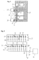
- figure 1 1 shows a scanning microscope 20 having at least one light source 22 .
- the light source 22 generates an illuminating light beam 23 which is focused on a sample 30 via a scanning unit 24 and a beam splitter 26 with the aid of a first lens 28 .
- a first detection beam 31 emanating from the sample in the direction of illumination is directed onto a first detector arrangement 36 via a second lens 32 and a mirror 34 .
- a second detection beam 40 emanating from the sample 30 counter to the direction of illumination is directed via the beam splitter 26 onto a second detector arrangement 38 .
- the detection beams 31 and 40 are not deflected using the scanning unit 24 .
- the first and second detector arrays 36, 38 are therefore also referred to as "non-descanned detectors" (NDD).
- NDD non-descanned detectors
- the scanning microscope 20 can also be referred to as a device comprising a microscope for examining the sample 30 .
- further detection beams can arise, which are fed back via the scanning unit 24 and which are detected using one or more detectors (not shown).
- the scanning microscope 20 can be a confocal scanning microscope.
- the first lens 28 focuses the illuminating light beam 23 onto a focal area on or in the sample 30.
- the focal area is point-shaped.
- the focus area can be designed in the form of a line, for example when using a line scanner.
- a closed scan field is preferably scanned optically.
- the focus area can also be moved in the z-direction perpendicular to the plane.
- the detection beams 31, 40 emanating from the sample 30 arise essentially from fluorescence effects which occur as a result of the illumination of the sample 30. Special effects, such as 2 or more photon effects, can also be used. Microscopy methods in which the devices according to the invention can be used, or effects that can be observed with the assembly 20 are in particular FLIM (Fluorescence Lifetime Imaging), FRAP (Fluorescence Recovery After Photobleaching), FRET (Fluorescence Resonance Energy Transfer) and FCS (Fluorescence Correlation -spectroscopy).
- FLIM Fluorescence Lifetime Imaging
- FRAP Fluorescence Recovery After Photobleaching
- FRET Fluorescence Resonance Energy Transfer
- FCS Fluorescence Correlation -spectroscopy
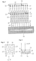
- each of the detector arrangements 36, 38 has two or more photosensitive semiconductor elements 50, as shown in FIG figure 2 shown.
- the photosensitive semiconductor elements 50 thus form the detector arrangements 36, 38, which can each also be referred to as a sensor array or detector array.
- Avalanche photo diodes are used as semiconductor elements 50 . These are operated in Geiger mode above their breakdown voltage. All individual pulses are summed up in analog form for evaluation, so that the overall signal is proportional to the number of incident photons. Alternatively or additionally, the individual pulses can be evaluated directly and counted in the measurement interval.
- the disadvantage that arises from using the avalanche photodiode in the Geiger mode, namely the longer dead time can be compensated for.
- analog summation and direct evaluation can be combined, as in figure 3 shown.
- figure 2 shows a possible circuit according to which the individual semiconductor elements 50 of a detector arrangement 36, 38 can be electrically connected to one another.
- the semiconductor elements 50 are connected in series with one series resistor 58 each, but in parallel with one another.
- the illustrated embodiment of the detector arrangement 36, 38 has a first row 52 and a second row 54 of semiconductor elements 50.
- the parallel-connected semiconductor elements 50 are connected via a single output line 60 to an amplifier 62, which transmits the signals from the semiconductor elements 50 to a common evaluation unit 64 reinforced.
- the evaluation unit 64 adds up the individual detection events in an analogous manner. After each detected event, one of the semiconductor elements 50 has a short dead time during which no new photon 56 can be detected.
- the use of several semiconductor elements 50 connected in parallel reduces the dead time for the entire detector arrangement 36, 38 since one of the semiconductor elements 50 can certainly detect a photon 56 while, for example, an adjacent semiconductor element 50 is currently in its dead time.
- the dead time can be further reduced if an assembly (not shown) is provided for resetting the semiconductor elements 50, the capacitance of the semiconductor elements 50 being resettable passively with the aid of the assembly.
- a separate circuit can be provided which actively resets the capacitance of the semiconductor elements 50 .
- figure 3 shows an alternative circuit of the semiconductor elements 50, in which two of the semiconductor elements 50 are connected in parallel to one another and are connected to the evaluation unit 64 via an output line 60 in each case.
- This circuit makes it possible to detect the individual signals of the two semiconductor elements 50 connected in parallel as a pair independently of the other pairs of semiconductor elements 50 . The detection events can then be summed up analogously and evaluated in pairs.
- the exemplary embodiments shown can easily be combined with one another by any number of semiconductor elements 50 connected in parallel being detected together via a common output 60 .
- the chip structure, in particular the number of outputs 60, can thus be specified in a simple manner.
- the Figures 4 and 5 show an embodiment in top view or side view, in which the quantum yield of the detector arrays 36, 38 is particularly large.
- the sides of the semiconductor elements 50 which face the detection beams 31, 40 have a light-sensitive area 70 which is as large as possible and as closed as possible.
- the fill factor on the light-sensitive surface is as large as possible.
- semiconductor elements 50 are used which are based on back-thinned technology, in which light-insensitive structures 74 of the semiconductor elements 50, for example contacts, are arranged on the side of the corresponding semiconductor element 50 facing away from the detection beams 31, 40.
- the quantum yield is increased further by arranging a lens 72 in front of each light-sensitive region 70 of a semiconductor element 50 .
- the lens 72 focuses the light of the detection light beams 31, 40 onto the light-sensitive area 70 of a semiconductor element 50.
- the individual lenses 72 can also be combined as a unit and are referred to as a lens arrangement or as a microlens array.
- the cooling device can, for example, have Peltier elements, in particular multi-stage Peltier elements.
- the detector arrangements 36, 38 can optionally be arranged in a protective atmosphere.
- the protective atmosphere prevents the formation of condensate on the photosensitive areas 70 of the semiconductor elements 50. This is particularly advantageous for detecting small signals which stand out only slightly or not at all from the dark noise without cooling or a protective atmosphere.
- the detection light beams 31, 40 are coupled into a light guide (not shown) before they are detected.
- a liquid light guide according to the invention is particularly advantageous because, on the one hand, it has relatively good transmission properties and, on the other hand, it can be produced with a relatively large diameter.
- the large diameter makes it easier to image even strongly deflected detection beams 31, 40 reliably onto the cross section of the corresponding light guide and thus onto one of the detector arrangements 36, 38 with approximately no effects on the detection quality.
- the invention is not limited to the specified exemplary embodiments.
- other light-sensitive components can also be used as semiconductor elements 50 for detector arrangements 36, 38.
- only one or more detector arrangements 36, 38 can be arranged.
- different detector arrangements 36, 38 can be provided.
- the scanning microscope can, instead of the scanning unit 24, comprise a scanning table on which the sample 30 is arranged and which moves the sample 30 under the illuminating light beam 23 directed onto the sample 30 and thereby a focal area of the illuminating light beam 23 moved within the predetermined scan field on or in the sample 30.
Landscapes
- Physics & Mathematics (AREA)
- Engineering & Computer Science (AREA)
- Computer Vision & Pattern Recognition (AREA)
- General Engineering & Computer Science (AREA)
- Chemical & Material Sciences (AREA)
- Analytical Chemistry (AREA)
- General Physics & Mathematics (AREA)
- Optics & Photonics (AREA)
- Microscoopes, Condenser (AREA)
Claims (5)
- Dispositif pour examiner un échantillon (30), comprenantun microscope,comprenant une source de lumière (22), qui génère un faisceau de lumière d'éclairage (23), une unité de balayage (24), qui dévie le faisceau de lumière d'éclairage (23) dirigé sur l'échantillon (30) via un objectif et déplace ainsi une zone de focalisation du faisceau de lumière d'éclairage (23) à l'intérieur d'un champ de balayage prédéfini sur ou dans l'échantillon (30),et comprenant au moins un arrangement détecteur (36), qui comporte deux éléments semiconducteurs photosensibles (50) ou plus et qui détecte un faisceau de lumière de détection (31, 40) émanant de l'échantillon (30) et non dévié par l'unité de balayage (24),le dispositif étant caractérisé en ce que lesdits deux éléments semiconducteurs (50) ou plus sont branchés électriquement en parallèle et sont reliés par le biais d'une ligne de sortie (60) commune à une unité d'interprétation (64), les éléments semiconducteurs (50) possédant respectivement une photodiode à avalanche qui, au-dessus de sa tension de claquage, fonctionne en mode Geiger, etque le trajet de faisceau de détection suit un tracé par un guide de lumière liquide.
- Dispositif selon la revendication 1, avec lequel une lentille (72) est respectivement disposée le long du trajet de faisceau de détection (40) devant chaque élément semiconducteur (50), laquelle focalise le faisceau de lumière détection (31, 40) sur l'élément semiconducteur (50) correspondant.
- Dispositif selon l'une des revendications précédentes, avec lequel les structures insensibles à la lumière (74) des éléments semiconducteurs (50) sont disposées sur un côté des éléments semiconducteurs (50) à l'opposé du faisceau de lumière détection (31, 40).
- Dispositif selon l'une des revendications précédentes, avec lequel l'arrangement détecteur (36) est disposé dans une atmosphère contrôlée et/ou est couplé thermiquement avec une unité de refroidissement.
- Dispositif selon l'une des revendications précédentes, comprenant un sous-ensemble destiné à réinitialiser les éléments semiconducteurs (50), lequel réinitialise passivement ou activement la capacité des éléments semiconducteurs (50).
Applications Claiming Priority (1)
| Application Number | Priority Date | Filing Date | Title |
|---|---|---|---|
| DE102009057304A DE102009057304A1 (de) | 2009-12-07 | 2009-12-07 | Vorrichtung zum Untersuchen einer Probe umfassend ein Mikroskop |
Publications (3)
| Publication Number | Publication Date |
|---|---|
| EP2336817A1 EP2336817A1 (fr) | 2011-06-22 |
| EP2336817B1 EP2336817B1 (fr) | 2020-06-17 |
| EP2336817B2 true EP2336817B2 (fr) | 2023-08-16 |
Family
ID=43638773
Family Applications (1)
| Application Number | Title | Priority Date | Filing Date |
|---|---|---|---|
| EP10193888.4A Active EP2336817B2 (fr) | 2009-12-07 | 2010-12-07 | Dispositif destiné à l'analyse d'un échantillon comprenant un microscope |
Country Status (2)
| Country | Link |
|---|---|
| EP (1) | EP2336817B2 (fr) |
| DE (1) | DE102009057304A1 (fr) |
Family Cites Families (9)
| Publication number | Priority date | Publication date | Assignee | Title |
|---|---|---|---|---|
| US6134002A (en) * | 1999-01-14 | 2000-10-17 | Duke University | Apparatus and method for the rapid spectral resolution of confocal images |
| US6734415B1 (en) * | 1999-10-07 | 2004-05-11 | Agilent Technologies, Inc. | High quantum efficiency point light detector |
| DE10253609A1 (de) * | 2002-11-15 | 2004-05-27 | Leica Microsystems Heidelberg Gmbh | Scanmikroskop |
| WO2005020194A1 (fr) * | 2003-08-22 | 2005-03-03 | E.I. Dupont De Nemours And Company | Procedes de verification d'identite utilisant des polymeres transparents et luminescents |
| DE102005059948A1 (de) * | 2005-01-31 | 2006-08-03 | Leica Microsystems Cms Gmbh | Detektor |
| US7329860B2 (en) * | 2005-11-23 | 2008-02-12 | Illumina, Inc. | Confocal imaging methods and apparatus |
| US7619732B2 (en) * | 2006-03-01 | 2009-11-17 | Leica Microsystems Cms Gmbh | Method and microscope for high spatial resolution examination of samples |
| US7990524B2 (en) * | 2006-06-30 | 2011-08-02 | The University Of Chicago | Stochastic scanning apparatus using multiphoton multifocal source |
| DE102007024074B4 (de) * | 2007-05-22 | 2022-09-15 | Leica Microsystems Cms Gmbh | Mikroskop |
-
2009
- 2009-12-07 DE DE102009057304A patent/DE102009057304A1/de active Pending
-
2010
- 2010-12-07 EP EP10193888.4A patent/EP2336817B2/fr active Active
Non-Patent Citations (6)
| Title |
|---|
| "Handbook of Biological Confocal Microscopy. 3rd Ed.", 1 January 2006, article PAWLEY JAMES B.: "Multi-Photon", pages: 447, 535 - 542 † |
| A.G. STEWART ET AL: "Properties of silicon photon counting detectors and silicon photomultipliers", JOURNAL OF MODERN OPTICS, vol. 56, no. 2-3, 20 January 2009 (2009-01-20), pages 240 - 252 † |
| GRIGORIEV, E. ET AL: "Silicon photomultipliers and their bio-medical applications", NUCLEAR INSTRUMENTS & METHODS IN PHYSICS RESEARCH. SECTION A, vol. 571, no. 1-2, 26 January 2007 (2007-01-26), pages 130 - 133 † |
| HAMAMATSU PHOTONICS - CATALOGUE: "MPPC Multi-Pixel Photon Counter", HAMAMATSU PHOTONICS - CATALOGUE, 1 January 2007 (2007-01-01), pages 1 - 16 † |
| N OTTE: "The Silicon Photomultiplier -A new device for High Energy Physics, Astroparticle Physics, Industrial and Medical Applications", SNIC SYMPOSIUM, STANFORD, CALIFORNIA, 3 April 2006 (2006-04-03), pages 1 - 9 † |
| WOKOSIN D.L., AMOS W.B., WHITE J.G.: "Detection sensitivity enhancements for fluorescence imaging with multi-photon excitation microscopy", ENGINEERING IN MEDICINE AND BIOLOGY SOCIETY,1998. PROCEEDINGS OF THE20TH ANNUAL INTERNATIONAL CONFERENCE OF THE IEEE, vol. 4, 29 October 1998 (1998-10-29) - 1 November 1998 (1998-11-01), pages 1707 - 1714 † |
Also Published As
| Publication number | Publication date |
|---|---|
| EP2336817B1 (fr) | 2020-06-17 |
| EP2336817A1 (fr) | 2011-06-22 |
| DE102009057304A1 (de) | 2011-06-09 |
Similar Documents
| Publication | Publication Date | Title |
|---|---|---|
| EP2149037B1 (fr) | Dispositif de détection de lumière dans un microscope à balayage | |
| EP2546621B1 (fr) | Dispositif et procédé de détection de lumière | |
| EP3526634B1 (fr) | Groupe optique pour une lumière de détection pour un microscope, procédé de microscopie et microscope | |
| EP0898783A2 (fr) | Microscope a balayage dans lequel un echantillon est excite optiquement simultanement en plusieurs points | |
| DE102013218795A1 (de) | Laserscanningmikroskop und Verfahren zur Korrektur von Abbildungsfehlern insbesondere in der hochauflösenden Scanning-Mikroskopie | |
| DE102020209889A1 (de) | Mikroskop und Verfahren zur mikroskopischen Bildaufnahme mit variabler Beleuchtung | |
| EP1664889B1 (fr) | Dispositif de detection de photons d'un rayon lumineux | |
| DE102020213715A1 (de) | Vorrichtung und Verfahren zur schnellen dreidimensionalen Erfassung von Bilddaten | |
| DE3340647A1 (de) | Verfahren zur fokussierung eines mikroskopes sowie mikroskop zur durchfuehrung des verfahrens | |
| DE102010055882A1 (de) | Pinhole für ein konfokales Laser-Scanning Mikroskop | |
| DE10004233A1 (de) | Mikroskop-Aufbau | |
| DE102017107615B3 (de) | Monozentrische Empfangsanordnung | |
| DE102004003993A1 (de) | Vorrichtung zum Nachweis von Photonen eines Lichtstrahls | |
| DE102013005927A1 (de) | Verfahren zum optisch hochaufgelösten Rasterscanning eines Objekts | |
| EP1168031A2 (fr) | Structure de microscope | |
| DE112017001734T5 (de) | Bilderfassungsvorrichtung und Bilderfassungsverfahren | |
| EP2336817B2 (fr) | Dispositif destiné à l'analyse d'un échantillon comprenant un microscope | |
| EP1929256A1 (fr) | Puce a photodetecteur, microscope a laser muni d'une puce a photodetecteur et procede pour selectionner une puce a photodetecteur | |
| DE10017824B4 (de) | Vorrichtung zur parallelen photometrischen Fluoreszenz- oder Lumineszenzanalyse mehrerer voneinander getrennter Probenbereiche auf einem Objekt | |
| WO2012069220A1 (fr) | Dispositif pour la mesure de la durée de vie d'un porteur de charge dans un substrat semi-conducteur | |
| EP1691180A2 (fr) | Détecteur avec un agencement de microlentilles | |
| EP1803157B1 (fr) | Detecteur emccd et spectrometre et microscope | |
| DE19707225A1 (de) | Lichtabtastvorrichtung | |
| DE10206004A1 (de) | Vorrichtung zur konfokalen optischen Mikroanalyse | |
| DE102020202804A1 (de) | Verfahren und Vorrichtung zur Bilderfassung |
Legal Events
| Date | Code | Title | Description |
|---|---|---|---|
| PUAI | Public reference made under article 153(3) epc to a published international application that has entered the european phase |
Free format text: ORIGINAL CODE: 0009012 |
|
| AK | Designated contracting states |
Kind code of ref document: A1 Designated state(s): AL AT BE BG CH CY CZ DE DK EE ES FI FR GB GR HR HU IE IS IT LI LT LU LV MC MK MT NL NO PL PT RO RS SE SI SK SM TR |
|
| AX | Request for extension of the european patent |
Extension state: BA ME |
|
| 17P | Request for examination filed |
Effective date: 20111222 |
|
| STAA | Information on the status of an ep patent application or granted ep patent |
Free format text: STATUS: EXAMINATION IS IN PROGRESS |
|
| 17Q | First examination report despatched |
Effective date: 20170313 |
|
| GRAP | Despatch of communication of intention to grant a patent |
Free format text: ORIGINAL CODE: EPIDOSNIGR1 |
|
| STAA | Information on the status of an ep patent application or granted ep patent |
Free format text: STATUS: GRANT OF PATENT IS INTENDED |
|
| INTG | Intention to grant announced |
Effective date: 20191216 |
|
| GRAS | Grant fee paid |
Free format text: ORIGINAL CODE: EPIDOSNIGR3 |
|
| GRAJ | Information related to disapproval of communication of intention to grant by the applicant or resumption of examination proceedings by the epo deleted |
Free format text: ORIGINAL CODE: EPIDOSDIGR1 |
|
| GRAL | Information related to payment of fee for publishing/printing deleted |
Free format text: ORIGINAL CODE: EPIDOSDIGR3 |
|
| STAA | Information on the status of an ep patent application or granted ep patent |
Free format text: STATUS: EXAMINATION IS IN PROGRESS |
|
| GRAR | Information related to intention to grant a patent recorded |
Free format text: ORIGINAL CODE: EPIDOSNIGR71 |
|
| STAA | Information on the status of an ep patent application or granted ep patent |
Free format text: STATUS: GRANT OF PATENT IS INTENDED |
|
| GRAA | (expected) grant |
Free format text: ORIGINAL CODE: 0009210 |
|
| STAA | Information on the status of an ep patent application or granted ep patent |
Free format text: STATUS: THE PATENT HAS BEEN GRANTED |
|
| INTC | Intention to grant announced (deleted) | ||
| AK | Designated contracting states |
Kind code of ref document: B1 Designated state(s): AL AT BE BG CH CY CZ DE DK EE ES FI FR GB GR HR HU IE IS IT LI LT LU LV MC MK MT NL NO PL PT RO RS SE SI SK SM TR |
|
| INTG | Intention to grant announced |
Effective date: 20200511 |
|
| REG | Reference to a national code |
Ref country code: GB Ref legal event code: FG4D Free format text: NOT ENGLISH |
|
| REG | Reference to a national code |
Ref country code: CH Ref legal event code: EP |
|
| REG | Reference to a national code |
Ref country code: DE Ref legal event code: R096 Ref document number: 502010016668 Country of ref document: DE |
|
| REG | Reference to a national code |
Ref country code: IE Ref legal event code: FG4D Free format text: LANGUAGE OF EP DOCUMENT: GERMAN |
|
| REG | Reference to a national code |
Ref country code: AT Ref legal event code: REF Ref document number: 1282033 Country of ref document: AT Kind code of ref document: T Effective date: 20200715 |
|
| PG25 | Lapsed in a contracting state [announced via postgrant information from national office to epo] |
Ref country code: FI Free format text: LAPSE BECAUSE OF FAILURE TO SUBMIT A TRANSLATION OF THE DESCRIPTION OR TO PAY THE FEE WITHIN THE PRESCRIBED TIME-LIMIT Effective date: 20200617 Ref country code: SE Free format text: LAPSE BECAUSE OF FAILURE TO SUBMIT A TRANSLATION OF THE DESCRIPTION OR TO PAY THE FEE WITHIN THE PRESCRIBED TIME-LIMIT Effective date: 20200617 Ref country code: LT Free format text: LAPSE BECAUSE OF FAILURE TO SUBMIT A TRANSLATION OF THE DESCRIPTION OR TO PAY THE FEE WITHIN THE PRESCRIBED TIME-LIMIT Effective date: 20200617 Ref country code: NO Free format text: LAPSE BECAUSE OF FAILURE TO SUBMIT A TRANSLATION OF THE DESCRIPTION OR TO PAY THE FEE WITHIN THE PRESCRIBED TIME-LIMIT Effective date: 20200917 Ref country code: GR Free format text: LAPSE BECAUSE OF FAILURE TO SUBMIT A TRANSLATION OF THE DESCRIPTION OR TO PAY THE FEE WITHIN THE PRESCRIBED TIME-LIMIT Effective date: 20200918 |
|
| REG | Reference to a national code |
Ref country code: LT Ref legal event code: MG4D |
|
| REG | Reference to a national code |
Ref country code: NL Ref legal event code: MP Effective date: 20200617 |
|
| PG25 | Lapsed in a contracting state [announced via postgrant information from national office to epo] |
Ref country code: RS Free format text: LAPSE BECAUSE OF FAILURE TO SUBMIT A TRANSLATION OF THE DESCRIPTION OR TO PAY THE FEE WITHIN THE PRESCRIBED TIME-LIMIT Effective date: 20200617 Ref country code: LV Free format text: LAPSE BECAUSE OF FAILURE TO SUBMIT A TRANSLATION OF THE DESCRIPTION OR TO PAY THE FEE WITHIN THE PRESCRIBED TIME-LIMIT Effective date: 20200617 Ref country code: HR Free format text: LAPSE BECAUSE OF FAILURE TO SUBMIT A TRANSLATION OF THE DESCRIPTION OR TO PAY THE FEE WITHIN THE PRESCRIBED TIME-LIMIT Effective date: 20200617 Ref country code: BG Free format text: LAPSE BECAUSE OF FAILURE TO SUBMIT A TRANSLATION OF THE DESCRIPTION OR TO PAY THE FEE WITHIN THE PRESCRIBED TIME-LIMIT Effective date: 20200917 |
|
| PG25 | Lapsed in a contracting state [announced via postgrant information from national office to epo] |
Ref country code: NL Free format text: LAPSE BECAUSE OF FAILURE TO SUBMIT A TRANSLATION OF THE DESCRIPTION OR TO PAY THE FEE WITHIN THE PRESCRIBED TIME-LIMIT Effective date: 20200617 Ref country code: AL Free format text: LAPSE BECAUSE OF FAILURE TO SUBMIT A TRANSLATION OF THE DESCRIPTION OR TO PAY THE FEE WITHIN THE PRESCRIBED TIME-LIMIT Effective date: 20200617 |
|
| PG25 | Lapsed in a contracting state [announced via postgrant information from national office to epo] |
Ref country code: SM Free format text: LAPSE BECAUSE OF FAILURE TO SUBMIT A TRANSLATION OF THE DESCRIPTION OR TO PAY THE FEE WITHIN THE PRESCRIBED TIME-LIMIT Effective date: 20200617 Ref country code: EE Free format text: LAPSE BECAUSE OF FAILURE TO SUBMIT A TRANSLATION OF THE DESCRIPTION OR TO PAY THE FEE WITHIN THE PRESCRIBED TIME-LIMIT Effective date: 20200617 Ref country code: CZ Free format text: LAPSE BECAUSE OF FAILURE TO SUBMIT A TRANSLATION OF THE DESCRIPTION OR TO PAY THE FEE WITHIN THE PRESCRIBED TIME-LIMIT Effective date: 20200617 Ref country code: IT Free format text: LAPSE BECAUSE OF FAILURE TO SUBMIT A TRANSLATION OF THE DESCRIPTION OR TO PAY THE FEE WITHIN THE PRESCRIBED TIME-LIMIT Effective date: 20200617 Ref country code: RO Free format text: LAPSE BECAUSE OF FAILURE TO SUBMIT A TRANSLATION OF THE DESCRIPTION OR TO PAY THE FEE WITHIN THE PRESCRIBED TIME-LIMIT Effective date: 20200617 Ref country code: ES Free format text: LAPSE BECAUSE OF FAILURE TO SUBMIT A TRANSLATION OF THE DESCRIPTION OR TO PAY THE FEE WITHIN THE PRESCRIBED TIME-LIMIT Effective date: 20200617 Ref country code: PT Free format text: LAPSE BECAUSE OF FAILURE TO SUBMIT A TRANSLATION OF THE DESCRIPTION OR TO PAY THE FEE WITHIN THE PRESCRIBED TIME-LIMIT Effective date: 20201019 |
|
| PG25 | Lapsed in a contracting state [announced via postgrant information from national office to epo] |
Ref country code: IS Free format text: LAPSE BECAUSE OF FAILURE TO SUBMIT A TRANSLATION OF THE DESCRIPTION OR TO PAY THE FEE WITHIN THE PRESCRIBED TIME-LIMIT Effective date: 20201017 Ref country code: PL Free format text: LAPSE BECAUSE OF FAILURE TO SUBMIT A TRANSLATION OF THE DESCRIPTION OR TO PAY THE FEE WITHIN THE PRESCRIBED TIME-LIMIT Effective date: 20200617 Ref country code: SK Free format text: LAPSE BECAUSE OF FAILURE TO SUBMIT A TRANSLATION OF THE DESCRIPTION OR TO PAY THE FEE WITHIN THE PRESCRIBED TIME-LIMIT Effective date: 20200617 |
|
| REG | Reference to a national code |
Ref country code: DE Ref legal event code: R026 Ref document number: 502010016668 Country of ref document: DE |
|
| PLBI | Opposition filed |
Free format text: ORIGINAL CODE: 0009260 |
|
| 26 | Opposition filed |
Opponent name: CARL ZEISS MICROSCOPY GMBH Effective date: 20210317 |
|
| PG25 | Lapsed in a contracting state [announced via postgrant information from national office to epo] |
Ref country code: DK Free format text: LAPSE BECAUSE OF FAILURE TO SUBMIT A TRANSLATION OF THE DESCRIPTION OR TO PAY THE FEE WITHIN THE PRESCRIBED TIME-LIMIT Effective date: 20200617 |
|
| PG25 | Lapsed in a contracting state [announced via postgrant information from national office to epo] |
Ref country code: SI Free format text: LAPSE BECAUSE OF FAILURE TO SUBMIT A TRANSLATION OF THE DESCRIPTION OR TO PAY THE FEE WITHIN THE PRESCRIBED TIME-LIMIT Effective date: 20200617 |
|
| PLAX | Notice of opposition and request to file observation + time limit sent |
Free format text: ORIGINAL CODE: EPIDOSNOBS2 |
|
| REG | Reference to a national code |
Ref country code: CH Ref legal event code: PL |
|
| PG25 | Lapsed in a contracting state [announced via postgrant information from national office to epo] |
Ref country code: MC Free format text: LAPSE BECAUSE OF FAILURE TO SUBMIT A TRANSLATION OF THE DESCRIPTION OR TO PAY THE FEE WITHIN THE PRESCRIBED TIME-LIMIT Effective date: 20200617 |
|
| REG | Reference to a national code |
Ref country code: BE Ref legal event code: MM Effective date: 20201231 |
|
| PLBB | Reply of patent proprietor to notice(s) of opposition received |
Free format text: ORIGINAL CODE: EPIDOSNOBS3 |
|
| PG25 | Lapsed in a contracting state [announced via postgrant information from national office to epo] |
Ref country code: LU Free format text: LAPSE BECAUSE OF NON-PAYMENT OF DUE FEES Effective date: 20201207 Ref country code: IE Free format text: LAPSE BECAUSE OF NON-PAYMENT OF DUE FEES Effective date: 20201207 |
|
| PG25 | Lapsed in a contracting state [announced via postgrant information from national office to epo] |
Ref country code: LI Free format text: LAPSE BECAUSE OF NON-PAYMENT OF DUE FEES Effective date: 20201231 Ref country code: CH Free format text: LAPSE BECAUSE OF NON-PAYMENT OF DUE FEES Effective date: 20201231 |
|
| REG | Reference to a national code |
Ref country code: AT Ref legal event code: MM01 Ref document number: 1282033 Country of ref document: AT Kind code of ref document: T Effective date: 20201207 |
|
| PG25 | Lapsed in a contracting state [announced via postgrant information from national office to epo] |
Ref country code: AT Free format text: LAPSE BECAUSE OF NON-PAYMENT OF DUE FEES Effective date: 20201207 |
|
| PG25 | Lapsed in a contracting state [announced via postgrant information from national office to epo] |
Ref country code: TR Free format text: LAPSE BECAUSE OF FAILURE TO SUBMIT A TRANSLATION OF THE DESCRIPTION OR TO PAY THE FEE WITHIN THE PRESCRIBED TIME-LIMIT Effective date: 20200617 Ref country code: MT Free format text: LAPSE BECAUSE OF FAILURE TO SUBMIT A TRANSLATION OF THE DESCRIPTION OR TO PAY THE FEE WITHIN THE PRESCRIBED TIME-LIMIT Effective date: 20200617 Ref country code: CY Free format text: LAPSE BECAUSE OF FAILURE TO SUBMIT A TRANSLATION OF THE DESCRIPTION OR TO PAY THE FEE WITHIN THE PRESCRIBED TIME-LIMIT Effective date: 20200617 |
|
| PG25 | Lapsed in a contracting state [announced via postgrant information from national office to epo] |
Ref country code: MK Free format text: LAPSE BECAUSE OF FAILURE TO SUBMIT A TRANSLATION OF THE DESCRIPTION OR TO PAY THE FEE WITHIN THE PRESCRIBED TIME-LIMIT Effective date: 20200617 |
|
| PG25 | Lapsed in a contracting state [announced via postgrant information from national office to epo] |
Ref country code: BE Free format text: LAPSE BECAUSE OF NON-PAYMENT OF DUE FEES Effective date: 20201231 |
|
| PLAB | Opposition data, opponent's data or that of the opponent's representative modified |
Free format text: ORIGINAL CODE: 0009299OPPO |
|
| R26 | Opposition filed (corrected) |
Opponent name: CARL ZEISS MICROSCOPY GMBH Effective date: 20210317 |
|
| P01 | Opt-out of the competence of the unified patent court (upc) registered |
Effective date: 20230414 |
|
| PUAH | Patent maintained in amended form |
Free format text: ORIGINAL CODE: 0009272 |
|
| STAA | Information on the status of an ep patent application or granted ep patent |
Free format text: STATUS: PATENT MAINTAINED AS AMENDED |
|
| 27A | Patent maintained in amended form |
Effective date: 20230816 |
|
| AK | Designated contracting states |
Kind code of ref document: B2 Designated state(s): AL AT BE BG CH CY CZ DE DK EE ES FI FR GB GR HR HU IE IS IT LI LT LU LV MC MK MT NL NO PL PT RO RS SE SI SK SM TR |
|
| REG | Reference to a national code |
Ref country code: DE Ref legal event code: R102 Ref document number: 502010016668 Country of ref document: DE |
|
| PGFP | Annual fee paid to national office [announced via postgrant information from national office to epo] |
Ref country code: GB Payment date: 20231219 Year of fee payment: 14 |
|
| PGFP | Annual fee paid to national office [announced via postgrant information from national office to epo] |
Ref country code: FR Payment date: 20231226 Year of fee payment: 14 |
|
| PGFP | Annual fee paid to national office [announced via postgrant information from national office to epo] |
Ref country code: DE Payment date: 20231227 Year of fee payment: 14 |