EP2333958A1 - Atomic oscillator and manufacturing method - Google Patents
Atomic oscillator and manufacturing method Download PDFInfo
- Publication number
- EP2333958A1 EP2333958A1 EP10192886A EP10192886A EP2333958A1 EP 2333958 A1 EP2333958 A1 EP 2333958A1 EP 10192886 A EP10192886 A EP 10192886A EP 10192886 A EP10192886 A EP 10192886A EP 2333958 A1 EP2333958 A1 EP 2333958A1
- Authority
- EP
- European Patent Office
- Prior art keywords
- light
- cavity
- alkali metal
- metal atoms
- receiving element
- Prior art date
- Legal status (The legal status is an assumption and is not a legal conclusion. Google has not performed a legal analysis and makes no representation as to the accuracy of the status listed.)
- Withdrawn
Links
- 238000004519 manufacturing process Methods 0.000 title claims description 20
- 150000001340 alkali metals Chemical group 0.000 claims abstract description 49
- 239000004065 semiconductor Substances 0.000 claims description 25
- 239000000758 substrate Substances 0.000 claims description 25
- 238000010030 laminating Methods 0.000 claims description 10
- 229910052751 metal Inorganic materials 0.000 claims description 4
- 239000002184 metal Substances 0.000 claims description 4
- 238000007789 sealing Methods 0.000 claims description 4
- 238000000151 deposition Methods 0.000 claims description 2
- 239000006059 cover glass Substances 0.000 description 20
- 229910052783 alkali metal Inorganic materials 0.000 description 7
- 238000005530 etching Methods 0.000 description 7
- 230000000694 effects Effects 0.000 description 3
- 238000000034 method Methods 0.000 description 2
- 230000005540 biological transmission Effects 0.000 description 1
- 238000001311 chemical methods and process Methods 0.000 description 1
- 238000004891 communication Methods 0.000 description 1
- 239000011521 glass Substances 0.000 description 1
- 230000010355 oscillation Effects 0.000 description 1
- 229910052701 rubidium Inorganic materials 0.000 description 1
- IGLNJRXAVVLDKE-UHFFFAOYSA-N rubidium atom Chemical compound [Rb] IGLNJRXAVVLDKE-UHFFFAOYSA-N 0.000 description 1
- 239000012780 transparent material Substances 0.000 description 1
Images


Classifications
-
- H—ELECTRICITY
- H03—ELECTRONIC CIRCUITRY
- H03L—AUTOMATIC CONTROL, STARTING, SYNCHRONISATION OR STABILISATION OF GENERATORS OF ELECTRONIC OSCILLATIONS OR PULSES
- H03L7/00—Automatic control of frequency or phase; Synchronisation
- H03L7/26—Automatic control of frequency or phase; Synchronisation using energy levels of molecules, atoms, or subatomic particles as a frequency reference
-
- G—PHYSICS
- G04—HOROLOGY
- G04F—TIME-INTERVAL MEASURING
- G04F5/00—Apparatus for producing preselected time intervals for use as timing standards
- G04F5/14—Apparatus for producing preselected time intervals for use as timing standards using atomic clocks
Definitions
- the present invention relates to an atomic oscillator and a manufacturing method, and more particularly to an atomic oscillator in which a light-emitting element, a gas cell and a light-receiving element are vertically stacked, and a manufacturing method of the same.
- a highly accurate and highly stable oscillator is indispensable as a clock source used for generation of a clock signal of a transmission apparatus or a reference frequency of a broadcast station.
- a rubidium atomic oscillator having a highly accurate and stable oscillation frequency is often used.
- a request for miniaturization of an atomic oscillator is increased, and the necessity to miniaturize the overall size including a gas cell is compelled.
- a manufacturing method in which the manufacturing cost can be reduced is requested in order to reduce the unit cost.
- Patent Document 1 discloses a structure of an atomic oscillator in which light emitted from a light source is refracted by a prism and passes through a gas cell, and is further refracted by a prism and is received by a light-receiving element.
- the related-art atomic oscillator as one means for improving the production efficiency, a manufacturing method is adopted in which plural gas cells are integrally formed, and are later diced into single chips.
- the structure is such that the light-emitting element, the gas cell, and the light-receiving element are laterally arranged on the substrate and a certain interval is ensured between the respective members, and further, the plural mirrors to refract the light are required.
- the miniaturization is realized in the whole unit.
- Patent Document 1 uses the expensive parts such as the prism, there is a problem that the unit cost is high.
- An advantage of some aspects of the invention is to provide an atomic oscillator in which at least a light-receiving element or a light-emitting element and a gas cell are formed on a semiconductor substrate, and other parts are laminated thereon, so that miniaturization and cost down can be realized.
- an atomic oscillator including a light-receiving element including a light-receiving section, a cell layer that is laminated on the light-receiving element and includes a cavity having an opening above the light-receiving section, gaseous alkali metal atoms sealed in the cavity, a transparent member to close the opening, and a light-emitting element to emit resonance light to the light-receiving section through the transparent member and the alkali metal atoms.
- the light-receiving element is formed on a semiconductor substrate. Further, the cell layer is laminated thereon, and the cavity having the opening on the opposite surface to the light-receiving element is formed by etching. The cell layer is placed in an alkali metal atom atmosphere, so that the cavity is filled with the alkali metal atoms. In this state, the opening is closed by the transparent member, and the light-emitting element is connected by a bump. By this, the monolithic atomic oscillator can be easily constructed.
- an atomic oscillator including a light-emitting element including a light-emitting section to emit resonance light, a cell layer that is laminated on the light-emitting element and includes a cavity having an opening above the light-emitting section, gaseous alkali metal atoms sealed in the cavity, a transparent member to close the opening, and a light-receiving element to receive the resonance light through the alkali metal atoms and the transparent member.
- the arrangement of the light-emitting element and the light-receiving element of the Application Example 1 is reversed. That is, the light-emitting element is formed on a semiconductor substrate. Further, the cell layer is laminated thereon, and the cavity having the opening on the opposite surface to the light-emitting element is formed by etching. This step can be realized by one step of a semiconductor process. The cell layer is placed in an alkali metal atom atmosphere, so that the cavity is filled with the alkali metal atoms. In that state, the opening is closed by the transparent member, and the light-receiving element is connected by a bump. By this, the monolithic atomic oscillator can be easily constructed.
- an atomic oscillator including a light-receiving element including a light-receiving section, a transparent member that is connected onto the light-receiving element and includes a cavity above the light-receiving section, gaseous alkali metal atoms sealed in the cavity, and a light-emitting element to emit resonance light to the alkali metal atoms through the transparent member.
- the step of closing the opening by the transparent member is omitted. That is, the light-emitting element is formed on a semiconductor substrate.
- the transparent member including the cavity is connected to the light-receiving element in an alkali metal atom atmosphere, so that the cavity is filled with the alkali metal atoms.
- the light-receiving element is connected by a bump.
- a manufacturing method of an atomic oscillator including forming a light-receiving element, which includes a light-receiving section, on a semiconductor substrate, laminating an oxide film on the light-receiving element, laminating a cell layer on the oxide film, forming a cavity in the cell layer to have an opening above the light-receiving section, sealing gaseous alkali metal atoms in the cavity, closing the opening by a transparent member, and connecting a light-emitting element, which emits resonance light to the alkali metal atoms, onto the opening.
- a manufacturing method of an atomic oscillator including forming a light-receiving element, which includes a light-receiving section, on a semiconductor substrate, laminating an oxide film on the light-receiving element, depositing alkali metal atoms on the oxide film, forming a transparent member including a cavity above the light-receiving section, connecting the transparent member to the light-receiving element, and connecting the light-emitting element, which emits resonance light to the alkali metal atoms, onto the transparent member.
- a manufacturing method of an atomic oscillator comprising:
- FIG. 1 is a sectional view showing a structure of an atomic oscillator of a first embodiment of the invention.
- FIG. 2 is a sectional view showing a structure of an atomic oscillator of a second embodiment of the invention.
- FIG. 3 is a sectional view showing a structure of an atomic oscillator of a third embodiment of the invention.
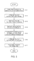
- FIG. 4 is a flowchart for explaining a manufacturing process of the atomic oscillator of FIG. 1 .
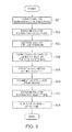
- FIG. 5 is a flowchart for explaining a manufacturing process of the atomic oscillator of FIG. 2 .
- FIG. 6 is a flowchart for explaining a manufacturing process of the atomic oscillator of FIG. 3 .
- FIG. 1 is a sectional view showing a structure of an atomic oscillator of a first embodiment of the invention.
- This atomic oscillator 50 includes a light-receiving element (PD: Photodiode) 6 that is formed on a semiconductor substrate and includes a light-receiving section 6a, a cell layer 8 that is laminated on the light-receiving element 6 and includes a cavity 8b having an opening 8a above the light-receiving section 6a, gaseous alkali metal atoms 5 sealed in the cavity 8b, a cover glass (transparent member) 4 to close the opening 8a, and a light-emitting element (VCSEL: Vertical Cavity Surface Emitting Laser) 1 to emit resonance light to the alkali metal atoms 5 through the cover glass 4.
- PD Light-receiving element
- a cell layer 8 that is laminated on the light-receiving element 6 and includes a cavity 8b having an opening 8a above the light-receiving section 6
- the light-receiving element (PD) 6 is provided with an electrode 7, and an electrode 3 for the light-emitting element 1 is formed on the cover glass 4.
- the light-emitting element is connected to the electrode 3 through a bump 2 of the light-emitting element 1.
- the light-receiving element 6 including the light-receiving section 6a is first formed on the semiconductor substrate. Further, the cell layer 8 is laminated thereon, and the cavity 8b having the opening 8a above the light-receiving section 6a is formed by etching.
- This structural body in the state where the cell layer 8 is mounted is placed in an alkali metal atom atmosphere, so that the cavity 8b is filled with the alkali metal atoms 5. In that state, the opening 8a is closed by the cover glass 4, and a cap having a recess is formed of the cover glass 4 and the cell layer 8.
- the light-emitting element 1 is connected to the electrode 3 on the upper surface of the cover glass 4 by the bump 2.
- plural cavities 8b are formed at desired positions. Thereafter, in order to close openings 8a in the state where alkali metal atoms are filled in the cavities 8b, a structural body is prepared in which the cover glass 4 in a wafer state is overlapped on the cell layer 8 in a wafer state and is connected thereto.
- the structural body is cut and solidified for every atomic oscillator or every part for the atomic oscillator in the state before the light-emitting elements 1 are mounted.
- the monolithic atomic oscillator can be easily constructed.
- the cell layer 8 in which the cavity 8b is formed may be prepared before it is mounted on the semiconductor substrate 6.
- FIG. 2 is a sectional view showing a structure of an atomic oscillator of a second embodiment of the invention.
- This atomic oscillator 51 includes a light-receiving element 6 (PD) that is formed on a semiconductor substrate and includes a light-receiving section 6a, a cover glass (transparent member) 4 that is connected onto the light-receiving element 6 and includes a cavity 4b above the light-receiving section 6a, gaseous alkali metal atoms 5 sealed in the cavity 4b, and a light-emitting element (VCSEL) 1 to emit resonance light to the alkali metal atoms 5 through the cover glass 4.
- PD light-receiving element 6
- cover glass transparent member
- VCSEL light-emitting element
- the light-receiving element (PD) 6 is provided with an electrode 7, and an electrode 3 for the light-emitting element 1 is formed on the cover glass 4.
- the light-emitting element is connected to the electrode 3 through a bump 2 of the light-emitting element 1.
- FIG. 1 a difference between FIG. 1 and FIG. 2 is that in FIG. 1 , after the cell layer 8 is mounted on the semiconductor substrate, the cavity 8b is formed, and the alkali metal atoms 5 in the cavity 8b are sealed by the plate-like cover glass 4, while in FIG. 2 , the light-receiving element 6 and a cap are previously separately formed, and both are connected while the alkali metal atoms 5 are sealed in the cavity 4b (a manufacturing method will be described later).
- a step of closing the opening by the cover glass can be omitted. That is, the light-receiving element 6 including the light-receiving section 6a is formed on the semiconductor substrate.
- the cap is prepared in which the cavity 4b is formed in, for example, glass as transparent material. Thereafter, the cap and the light-receiving element 6 are overlapped with and connected to each other in an alkali metal atom atmosphere while the light-receiving section 6a is located in the opening of the cavity 4b, so that the cavity 4b is filled with the alkali metal atoms 5.
- the light-emitting element 1 is connected by the bump 2.
- the light-receiving element 6 and the cap are separately prepared, and both may be connected to each other in the alkali metal atom atmosphere.
- FIG. 3 is a sectional view showing a structure of an atomic oscillator of a third embodiment of the invention.
- This atomic oscillator 52 includes a light-emitting element (VCSEL) 1 that is formed on a semiconductor substrate and includes a light-emitting section 1a, a cell layer 8 that is laminated on the light-emitting element 1 and includes a cavity 8b having an opening 8a above the light-emitting section 1a, gaseous alkali metal atoms 5 sealed in the cavity 8b, a cover glass (transparent member) 4 to close the opening 8a, and a light-receiving element (PD) 6 to receive resonance light, which passes through the alkali metal atoms 5, through the cover glass 4.
- VCSEL light-emitting element
- the light--emitting element (VCSEL) 1 is provided with an electrode 10, and an electrode 3 for the light-receiving element 6 is formed on the cover glass 4.
- the light-receiving element is connected to the electrode 3 through a bump 2 of the light-receiving element 6 .
- FIG. 1 A difference between FIG. 1 and FIG. 3 is that in FIG. 1 , the cavity 8b is formed in the cell layer 8 laminated on the light-receiving element 6, while in FIG. 3 , the cavity 8b is formed in the cell layer 8 laminated on the light-emitting element 1.
- the arrangement of the light-emitting element 1 and the light-receiving element 6 of FIG. 1 is reversed. That is, the light-emitting element 1 including the light-emitting section 1a is formed on the semiconductor substrate. Further, the cell layer 8 is laminated thereon, and the cavity 8b having the opening 8a above the light-emitting section 1a is formed by etching. The cell layer 8 is placed in an alkali metal atom atmosphere, so that the cavity 8b is filled with the alkali metal atoms 5. In that state, the opening 8a is closed by the cover glass 4, and the light-receiving element 6 is connected by the bump 2. By this, the monolithic atomic oscillator can be easily constructed.
- FIG. 4 is a flowchart for explaining a manufacturing process of the atomic oscillator of FIG. 1 .
- the light-receiving element 6 is formed on the semiconductor substrate (S1) , and a metal film (hereinafter simply referred to as an electrode 7) for extracting an electrode is formed (S2) .
- the cell layer is laminated on the light-receiving element 6 (S3) .
- the cavity 8b is formed by etching a part of the cell layer (S4) .
- the opening 8a is provided on one side of the cavity 8b.
- the gaseous alkali metal atoms 5 are sealed in the cavity 8b (S5), and the cover glass 4 is connected to close the opening 8a (S6).
- the electrode 3 is formed on the cover glass 4 (S7) . Finally, the light-emitting element 1 to emit resonance light to the alkali metal atoms 5 is mounted above the opening 8a, and the electrode 3 and the bump 2 are connected (flip-chip bonding) (S8).
- FIG. 5 is a flowchart for explaining a manufacturing process of the atomic oscillator of FIG. 2 .
- the light-receiving element 6 is formed on the semiconductor substrate (S11), and further, the electrode 7 is formed (S12).
- an oxide film 9 is laminated on the light-receiving element 6 (S13) .
- Alkali metal atoms are deposited on a portion A of FIG. 2 (S14).
- the cap including the cavity 4b at the position opposite to the light-receiving element 6 is connected from above (S15) .
- the electrode 3 is formed on the cap (S16) .
- the light-emitting element 1 to emit resonance light to the alkali metal atoms 5 is mounted on the cap, and the electrode 3 and the bump 2 are connected (flip-chip bonding) (S17).
- FIG. 6 is a flowchart for explaining a manufacturing process of the atomic oscillator of FIG. 3 .
- the light-emitting element 1 is formed on the semiconductor substrate (S21), and further, the electrode 10 is formed (S22) .
- the cell layer 8 is laminated on the light-emitting element 1 (S23).
- the cavity 8b is formed by etching a part of the cell layer 8 (S24) .
- the gaseous alkali metal atoms 5 are sealed in the cavity 8b (S25), and the cover glass 4 is connected to close the opening 8a (S26).
- the electrode 3 is formed on the cover glass 4 (S27).
- the light-receiving element 6 to receive resonance light is mounted above the opening 8a, and the electrode 3 and the bump 2 are connected (flip-chip bonding) (S28) .
Landscapes
- Physics & Mathematics (AREA)
- General Physics & Mathematics (AREA)
- Spectroscopy & Molecular Physics (AREA)
- Stabilization Of Oscillater, Synchronisation, Frequency Synthesizers (AREA)
- Semiconductor Lasers (AREA)
Abstract
An atomic oscillator includes: a light-receiving element including a light-receiving section; a cell layer that is laminated on the light-receiving element and includes a cavity having an opening above the light-receiving section; gaseous alkali metal atoms sealed in the cavity; a transparent member to close the opening; and a light-emitting element to emit resonance light to the light-receiving section through the transparent member and the alkali metal atoms.
Description
- The present invention relates to an atomic oscillator and a manufacturing method, and more particularly to an atomic oscillator in which a light-emitting element, a gas cell and a light-receiving element are vertically stacked, and a manufacturing method of the same.
- In recent years, as the development of a digital network, such as a communication network or a broadcast network, proceeds, a highly accurate and highly stable oscillator is indispensable as a clock source used for generation of a clock signal of a transmission apparatus or a reference frequency of a broadcast station. As such an oscillator, a rubidium atomic oscillator having a highly accurate and stable oscillation frequency is often used. Besides, in recent years, a request for miniaturization of an atomic oscillator is increased, and the necessity to miniaturize the overall size including a gas cell is compelled. At the same time, a manufacturing method in which the manufacturing cost can be reduced is requested in order to reduce the unit cost.
-
US 6,900,702 B2 (Patent Document 1) discloses a structure of an atomic oscillator in which light emitted from a light source is refracted by a prism and passes through a gas cell, and is further refracted by a prism and is received by a light-receiving element. - In the related-art atomic oscillator, as one means for improving the production efficiency, a manufacturing method is adopted in which plural gas cells are integrally formed, and are later diced into single chips. However, the structure is such that the light-emitting element, the gas cell, and the light-receiving element are laterally arranged on the substrate and a certain interval is ensured between the respective members, and further, the plural mirrors to refract the light are required. Thus, it can not be necessarily said that the miniaturization is realized in the whole unit.
- Besides, since the related art disclosed in
Patent Document 1 uses the expensive parts such as the prism, there is a problem that the unit cost is high. - An advantage of some aspects of the invention is to provide an atomic oscillator in which at least a light-receiving element or a light-emitting element and a gas cell are formed on a semiconductor substrate, and other parts are laminated thereon, so that miniaturization and cost down can be realized.
- The invention can be realized as following embodiments or application examples.
- According to this application example of the invention, there is provided an atomic oscillator including a light-receiving element including a light-receiving section, a cell layer that is laminated on the light-receiving element and includes a cavity having an opening above the light-receiving section, gaseous alkali metal atoms sealed in the cavity, a transparent member to close the opening, and a light-emitting element to emit resonance light to the light-receiving section through the transparent member and the alkali metal atoms.
- In this application example of the invention, first, the light-receiving element is formed on a semiconductor substrate. Further, the cell layer is laminated thereon, and the cavity having the opening on the opposite surface to the light-receiving element is formed by etching. The cell layer is placed in an alkali metal atom atmosphere, so that the cavity is filled with the alkali metal atoms. In this state, the opening is closed by the transparent member, and the light-emitting element is connected by a bump. By this, the monolithic atomic oscillator can be easily constructed.
- According to this application example of the invention, there is provided an atomic oscillator including a light-emitting element including a light-emitting section to emit resonance light, a cell layer that is laminated on the light-emitting element and includes a cavity having an opening above the light-emitting section, gaseous alkali metal atoms sealed in the cavity, a transparent member to close the opening, and a light-receiving element to receive the resonance light through the alkali metal atoms and the transparent member.
- In the structure of this application example of the invention, the arrangement of the light-emitting element and the light-receiving element of the Application Example 1 is reversed. That is, the light-emitting element is formed on a semiconductor substrate. Further, the cell layer is laminated thereon, and the cavity having the opening on the opposite surface to the light-emitting element is formed by etching. This step can be realized by one step of a semiconductor process. The cell layer is placed in an alkali metal atom atmosphere, so that the cavity is filled with the alkali metal atoms. In that state, the opening is closed by the transparent member, and the light-receiving element is connected by a bump. By this, the monolithic atomic oscillator can be easily constructed.
- According to this application example of the invention, there is provided an atomic oscillator including a light-receiving element including a light-receiving section, a transparent member that is connected onto the light-receiving element and includes a cavity above the light-receiving section, gaseous alkali metal atoms sealed in the cavity, and a light-emitting element to emit resonance light to the alkali metal atoms through the transparent member.
- In this application example of the invention, the step of closing the opening by the transparent member is omitted. That is, the light-emitting element is formed on a semiconductor substrate. The transparent member including the cavity is connected to the light-receiving element in an alkali metal atom atmosphere, so that the cavity is filled with the alkali metal atoms. The light-receiving element is connected by a bump. By this, the monolithic atomic oscillator can be easily constructed.
- According to this application example of the invention, there is provided a manufacturing method of an atomic oscillator including forming a light-receiving element, which includes a light-receiving section, on a semiconductor substrate, laminating an oxide film on the light-receiving element, laminating a cell layer on the oxide film, forming a cavity in the cell layer to have an opening above the light-receiving section, sealing gaseous alkali metal atoms in the cavity, closing the opening by a transparent member, and connecting a light-emitting element, which emits resonance light to the alkali metal atoms, onto the opening.
- The same operation and effect as those of Application Example 1 are obtained.
- According to this application example of the invention, there is provided a manufacturing method of an atomic oscillator including forming a light-receiving element, which includes a light-receiving section, on a semiconductor substrate, laminating an oxide film on the light-receiving element, depositing alkali metal atoms on the oxide film, forming a transparent member including a cavity above the light-receiving section, connecting the transparent member to the light-receiving element, and connecting the light-emitting element, which emits resonance light to the alkali metal atoms, onto the transparent member.
- The same operation and effect as those of Application Example 3 are obtained.
- According to this application example of the invention, there is provided a manufacturing method of an atomic oscillator, comprising:
- forming a light-emitting element, which includes a light-emitting section, on a semi-conductor substrate;
- laminating an oxide film on the light-emitting element;
- laminating a cell layer on the oxide film;
- forming a cavity in the cell layer to have an opening above the light-emitting section;
- sealing gaseous alkaline metal atoms in the cavity;
- closing the opening by a transparent member; and
- connecting a light-receiving element, which receives resonance light to the alkaline atoms, onto the opening.
- The invention will be described with reference to the accompanying drawing, wherein like numbers reference like elements.
-
FIG. 1 is a sectional view showing a structure of an atomic oscillator of a first embodiment of the invention. -
FIG. 2 is a sectional view showing a structure of an atomic oscillator of a second embodiment of the invention. -
FIG. 3 is a sectional view showing a structure of an atomic oscillator of a third embodiment of the invention. -
FIG. 4 is a flowchart for explaining a manufacturing process of the atomic oscillator ofFIG. 1 . -
FIG. 5 is a flowchart for explaining a manufacturing process of the atomic oscillator ofFIG. 2 . -
FIG. 6 is a flowchart for explaining a manufacturing process of the atomic oscillator ofFIG. 3 . - Hereinafter, embodiments of the invention will be described in detail with reference to the drawings. However, components, kinds, combinations, shapes, relative arrangement thereof and the like disclosed in the embodiments are not intended to limit the scope of the invention but are illustrative only.
-
FIG. 1 is a sectional view showing a structure of an atomic oscillator of a first embodiment of the invention. Thisatomic oscillator 50 includes a light-receiving element (PD: Photodiode) 6 that is formed on a semiconductor substrate and includes a light-receivingsection 6a, acell layer 8 that is laminated on the light-receivingelement 6 and includes acavity 8b having anopening 8a above the light-receivingsection 6a, gaseousalkali metal atoms 5 sealed in thecavity 8b, a cover glass (transparent member) 4 to close theopening 8a, and a light-emitting element (VCSEL: Vertical Cavity Surface Emitting Laser) 1 to emit resonance light to thealkali metal atoms 5 through thecover glass 4. The light-receiving element (PD) 6 is provided with anelectrode 7, and anelectrode 3 for the light-emittingelement 1 is formed on thecover glass 4. The light-emitting element is connected to theelectrode 3 through abump 2 of the light-emittingelement 1. - That is, in the embodiment of the invention, the light-receiving
element 6 including the light-receivingsection 6a is first formed on the semiconductor substrate. Further, thecell layer 8 is laminated thereon, and thecavity 8b having theopening 8a above the light-receivingsection 6a is formed by etching. This structural body in the state where thecell layer 8 is mounted is placed in an alkali metal atom atmosphere, so that thecavity 8b is filled with thealkali metal atoms 5. In that state, theopening 8a is closed by thecover glass 4, and a cap having a recess is formed of thecover glass 4 and thecell layer 8. - The light-emitting
element 1 is connected to theelectrode 3 on the upper surface of thecover glass 4 by thebump 2. - Incidentally, in order to efficiently form plural atomic oscillators, it is desirable to adopt a batch processing process.
- That is, after the
cell layer 8 in a wafer state is overlapped on the semiconductor substrate in a wafer state in which plural light-receivingsections 6a are formed,plural cavities 8b are formed at desired positions. Thereafter, in order to closeopenings 8a in the state where alkali metal atoms are filled in thecavities 8b, a structural body is prepared in which thecover glass 4 in a wafer state is overlapped on thecell layer 8 in a wafer state and is connected thereto. - At a stage before the light-emitting
elements 1 are mounted on the structural body or after the light-emittingelements 1 are mounted thereon, the structural body is cut and solidified for every atomic oscillator or every part for the atomic oscillator in the state before the light-emittingelements 1 are mounted. By this, the monolithic atomic oscillator can be easily constructed. - Incidentally, the
cell layer 8 in which thecavity 8b is formed may be prepared before it is mounted on thesemiconductor substrate 6. -
FIG. 2 is a sectional view showing a structure of an atomic oscillator of a second embodiment of the invention. Thisatomic oscillator 51 includes a light-receiving element 6 (PD) that is formed on a semiconductor substrate and includes a light-receivingsection 6a, a cover glass (transparent member) 4 that is connected onto the light-receivingelement 6 and includes acavity 4b above the light-receivingsection 6a, gaseousalkali metal atoms 5 sealed in thecavity 4b, and a light-emitting element (VCSEL) 1 to emit resonance light to thealkali metal atoms 5 through thecover glass 4. The light-receiving element (PD) 6 is provided with anelectrode 7, and anelectrode 3 for the light-emittingelement 1 is formed on thecover glass 4. The light-emitting element is connected to theelectrode 3 through abump 2 of the light-emittingelement 1. Here, a difference betweenFIG. 1 and FIG. 2 is that inFIG. 1 , after thecell layer 8 is mounted on the semiconductor substrate, thecavity 8b is formed, and thealkali metal atoms 5 in thecavity 8b are sealed by the plate-like cover glass 4, while inFIG. 2 , the light-receivingelement 6 and a cap are previously separately formed, and both are connected while thealkali metal atoms 5 are sealed in thecavity 4b (a manufacturing method will be described later). - That is, in this embodiment, a step of closing the opening by the cover glass can be omitted. That is, the light-receiving
element 6 including the light-receivingsection 6a is formed on the semiconductor substrate. The cap is prepared in which thecavity 4b is formed in, for example, glass as transparent material. Thereafter, the cap and the light-receivingelement 6 are overlapped with and connected to each other in an alkali metal atom atmosphere while the light-receivingsection 6a is located in the opening of thecavity 4b, so that thecavity 4b is filled with thealkali metal atoms 5. The light-emittingelement 1 is connected by thebump 2. By this, the monolithic atomic oscillator can be easily constructed without fear of damaging the light-receivingsection 6a by a chemical process such as etching. - Incidentally, also in the case of the monolithic atomic oscillator shown in
FIG. 1 , the light-receivingelement 6 and the cap are separately prepared, and both may be connected to each other in the alkali metal atom atmosphere. -
FIG. 3 is a sectional view showing a structure of an atomic oscillator of a third embodiment of the invention. Thisatomic oscillator 52 includes a light-emitting element (VCSEL) 1 that is formed on a semiconductor substrate and includes a light-emittingsection 1a, acell layer 8 that is laminated on the light-emittingelement 1 and includes acavity 8b having anopening 8a above the light-emittingsection 1a, gaseousalkali metal atoms 5 sealed in thecavity 8b, a cover glass (transparent member) 4 to close theopening 8a, and a light-receiving element (PD) 6 to receive resonance light, which passes through thealkali metal atoms 5, through thecover glass 4. Incidentally, the light--emitting element (VCSEL) 1 is provided with anelectrode 10, and anelectrode 3 for the light-receivingelement 6 is formed on thecover glass 4. The light-receiving element is connected to theelectrode 3 through abump 2 of the light-receivingelement 6 . A difference betweenFIG. 1 andFIG. 3 is that inFIG. 1 , thecavity 8b is formed in thecell layer 8 laminated on the light-receivingelement 6, while inFIG. 3 , thecavity 8b is formed in thecell layer 8 laminated on the light-emittingelement 1. - That is, in this embodiment, the arrangement of the light-emitting
element 1 and the light-receivingelement 6 ofFIG. 1 is reversed. That is, the light-emittingelement 1 including the light-emittingsection 1a is formed on the semiconductor substrate. Further, thecell layer 8 is laminated thereon, and thecavity 8b having theopening 8a above the light-emittingsection 1a is formed by etching. Thecell layer 8 is placed in an alkali metal atom atmosphere, so that thecavity 8b is filled with thealkali metal atoms 5. In that state, theopening 8a is closed by thecover glass 4, and the light-receivingelement 6 is connected by thebump 2. By this, the monolithic atomic oscillator can be easily constructed. -
FIG. 4 is a flowchart for explaining a manufacturing process of the atomic oscillator ofFIG. 1 . First, the light-receivingelement 6 is formed on the semiconductor substrate (S1) , and a metal film (hereinafter simply referred to as an electrode 7) for extracting an electrode is formed (S2) . Next, the cell layer is laminated on the light-receiving element 6 (S3) . Thecavity 8b is formed by etching a part of the cell layer (S4) . At this time, theopening 8a is provided on one side of thecavity 8b. Next, the gaseousalkali metal atoms 5 are sealed in thecavity 8b (S5), and thecover glass 4 is connected to close theopening 8a (S6). Theelectrode 3 is formed on the cover glass 4 (S7) . Finally, the light-emittingelement 1 to emit resonance light to thealkali metal atoms 5 is mounted above theopening 8a, and theelectrode 3 and thebump 2 are connected (flip-chip bonding) (S8). -
FIG. 5 is a flowchart for explaining a manufacturing process of the atomic oscillator ofFIG. 2 . First, the light-receivingelement 6 is formed on the semiconductor substrate (S11), and further, theelectrode 7 is formed (S12). Next, anoxide film 9 is laminated on the light-receiving element 6 (S13) . Alkali metal atoms are deposited on a portion A ofFIG. 2 (S14). The cap including thecavity 4b at the position opposite to the light-receivingelement 6 is connected from above (S15) . Theelectrode 3 is formed on the cap (S16) . Finally, the light-emittingelement 1 to emit resonance light to thealkali metal atoms 5 is mounted on the cap, and theelectrode 3 and thebump 2 are connected (flip-chip bonding) (S17). -
FIG. 6 is a flowchart for explaining a manufacturing process of the atomic oscillator ofFIG. 3 . First, the light-emittingelement 1 is formed on the semiconductor substrate (S21), and further, theelectrode 10 is formed (S22) . Next, thecell layer 8 is laminated on the light-emitting element 1 (S23). Thecavity 8b is formed by etching a part of the cell layer 8 (S24) . Next, the gaseousalkali metal atoms 5 are sealed in thecavity 8b (S25), and thecover glass 4 is connected to close theopening 8a (S26). Theelectrode 3 is formed on the cover glass 4 (S27). Finally, the light-receivingelement 6 to receive resonance light is mounted above theopening 8a, and theelectrode 3 and thebump 2 are connected (flip-chip bonding) (S28) .
Claims (10)
- An atomic oscillator comprising:a light-receiving element (6) including a light-receiving section (6a);a cell layer (8) that is laminated on the light-receiving element (6) and includes a cavity (8b) having an opening (8a) above the light-receiving section (6a);gaseous alkali metal atoms (5) sealed in the cavity (8b);a transparent member (4) to close the opening (8a); anda light-emitting element (1) to emit resonance light to the light-receiving section (6a) through the transparent member (4) and the alkali metal atoms (5).
- An atomic oscillator comprising:a light-emitting element (1) including a light-emitting section (1a) to emit resonance light;a cell layer (8) that is laminated on the light-emitting element (1) and includes a cavity (8b) having an opening (8a) above the light-emitting section (1a);gaseous alkali metal atoms (5) sealed in the cavity (8b);a transparent member (4) to close the opening (8a); anda light-receiving element (6) to receive the resonance light through the alkali metal atoms (5) and the transparent member (4).
- An atomic oscillator comprising:a. light-receiving element (6) including a light-receiving section (6a);a transparent member (4) that is connected onto the light-receiving element (6) and includes a cavity (4b) above the light-receiving section (6a);gaseous alkali metal atoms (5) sealed in the cavity (4b); anda light-emitting element (1) to emit resonance light to the alkali metal atoms (5) through the transparent member (4).
- An atomic oscillator according to claim 1 or claim 3, further comprising an electrode (3) for the light-emitting element (1) formed on the transparent member (4).
- An atomic oscillator according to claim 2, further comprising an electrode (3) for the light-receiving element (6) formed on the transparent member (4).
- An atomic oscillator according to claim 1, claim 3 or claim 4, wherein the light-receiving element (6) including the light-receiving section (6a) is formed on the semi-conductor substrate.
- An atomic oscillator according to claim 2 or claim 5, wherein the light-emitting element (1) including the light-emitting section (1a) is formed on the semi-conductor substrate (10).
- A manufacturing method of an atomic oscillator, comprising:forming a light-receiving element (6), which includes a light-receiving section (6a), on a semiconductor substrate (7);laminating an oxide film on the light-receiving element (6) ;laminating a cell layer (8) on the oxide film;forming a cavity (8b) in the cell layer (8) to have an opening (8a) above the light-receiving section (6a);sealing gaseous alkali metal atoms (5) in the cavity (8b);closing the opening (8a) by a transparent member (4); andconnecting a light-emitting element (1), which emits resonance light to the alkali metal atoms (5), onto the opening (8a).
- A manufacturing method of an atomic oscillator, comprising:forming a light-emitting element (1), which includes a light-emitting section (1a), on a semi-conductor substrate (10) ;laminating an oxide film on the light-emitting element;laminating a cell layer (8) on the oxide film;forming a cavity (8b) in the cell layer (8) to have an opening (8a) above the light-emitting section (1a);sealing gaseous alkaline metal atoms (5) in the cavity (8a);closing the opening by a transparent member (4); andconnecting a light-receiving element (6), which receives resonance light to the alkaline metal atoms (5), onto the opening (8a).
- A manufacturing method of an atomic oscillator, comprising:forming a light-receiving element, which includes a light-receiving section, on a semiconductor substrate;laminating an oxide film on the light-receiving element;depositing alkali metal atoms on the oxide film;forming a transparent member including a cavity above the light-receiving section;connecting the transparent member to the light-receiving element; andconnecting the light-emitting element, which emits resonance light to the alkali metal atoms, onto the transparent member.
Applications Claiming Priority (1)
| Application Number | Priority Date | Filing Date | Title |
|---|---|---|---|
| JP2009273157A JP5504851B2 (en) | 2009-12-01 | 2009-12-01 | Atomic oscillator and manufacturing method |
Publications (1)
| Publication Number | Publication Date |
|---|---|
| EP2333958A1 true EP2333958A1 (en) | 2011-06-15 |
Family
ID=43502977
Family Applications (1)
| Application Number | Title | Priority Date | Filing Date |
|---|---|---|---|
| EP10192886A Withdrawn EP2333958A1 (en) | 2009-12-01 | 2010-11-29 | Atomic oscillator and manufacturing method |
Country Status (4)
| Country | Link |
|---|---|
| US (1) | US8710934B2 (en) |
| EP (1) | EP2333958A1 (en) |
| JP (1) | JP5504851B2 (en) |
| CN (1) | CN102118165B (en) |
Families Citing this family (18)
| Publication number | Priority date | Publication date | Assignee | Title |
|---|---|---|---|---|
| JP5821439B2 (en) * | 2011-02-16 | 2015-11-24 | セイコーエプソン株式会社 | Gas cell manufacturing method |
| US8624682B2 (en) * | 2011-06-13 | 2014-01-07 | Honeywell International Inc. | Vapor cell atomic clock physics package |
| CN102323738B (en) * | 2011-07-20 | 2014-04-02 | 中国科学院上海微系统与信息技术研究所 | Groove type atomic gas cavity and atomic clock physical system formed by same |
| US9568565B2 (en) * | 2013-07-23 | 2017-02-14 | Texas Instruments Incorporated | Vapor cell structure having cavities connected by channels for micro-fabricated atomic clocks, magnetometers, and other devices |
| WO2015019471A1 (en) * | 2013-08-08 | 2015-02-12 | 株式会社日立製作所 | Magnetic field measuring device |
| JP2015118962A (en) * | 2013-12-16 | 2015-06-25 | セイコーエプソン株式会社 | Quantum interference devices, atomic oscillators, electronic equipment, and moving objects |
| JP6323650B2 (en) * | 2013-12-20 | 2018-05-16 | セイコーエプソン株式会社 | Surface emitting laser and atomic oscillator |
| US9454135B2 (en) * | 2014-06-19 | 2016-09-27 | Texas Instruments Incorporated | Manufactureable long cell with enhanced sensitivity and good mechanical strength |
| JP6488599B2 (en) * | 2014-09-08 | 2019-03-27 | セイコーエプソン株式会社 | Quantum interferometer, atomic cell manufacturing method, and electronic apparatus |
| US9639062B2 (en) * | 2015-03-30 | 2017-05-02 | Texas Instruments Incorporated | Vapor cell and method for making same |
| US10718661B2 (en) * | 2017-06-14 | 2020-07-21 | Texas Instruments Incorporated | Integrated microfabricated vapor cell sensor with transparent body having two intersecting signal paths |
| US10364144B2 (en) * | 2017-11-17 | 2019-07-30 | Texas Instruments Incorporated | Hermetically sealed package for mm-wave molecular spectroscopy cell |
| US10370760B2 (en) * | 2017-12-15 | 2019-08-06 | Texas Instruments Incorporated | Methods for gas generation in a sealed gas cell cavity |
| US11600581B2 (en) | 2021-04-15 | 2023-03-07 | Texas Instruments Incorporated | Packaged electronic device and multilevel lead frame coupler |
| US12444702B2 (en) | 2021-08-02 | 2025-10-14 | Texas Instruments Incorporated | Flip-chip enhanced quad flat no-lead electronic device with conductor backed coplanar waveguide transmission line feed in multilevel package substrate |
| US12519070B2 (en) | 2022-12-27 | 2026-01-06 | Texas Instruments Incorporated | System, electronic device and package with vertical to horizontal substrate integrated waveguide transition and horizontal grounded coplanar waveguide transition |
| US12489211B2 (en) | 2023-03-15 | 2025-12-02 | Texas Instruments Incorporated | Electronic device with patch antenna in packaging substrate |
| US12559363B2 (en) | 2023-08-28 | 2026-02-24 | Texas Instruments Incorporated | High reliability sensor |
Citations (2)
| Publication number | Priority date | Publication date | Assignee | Title |
|---|---|---|---|---|
| US6900702B2 (en) | 2002-08-14 | 2005-05-31 | Honeywell International Inc. | MEMS frequency standard for devices such as atomic clock |
| US20050184815A1 (en) * | 2004-01-06 | 2005-08-25 | Lipp Steven A. | Anodically bonded cell, method for making same and systems incorporating same |
Family Cites Families (6)
| Publication number | Priority date | Publication date | Assignee | Title |
|---|---|---|---|---|
| US6806784B2 (en) * | 2001-07-09 | 2004-10-19 | The National Institute Of Standards And Technology | Miniature frequency standard based on all-optical excitation and a micro-machined containment vessel |
| DE602005027217D1 (en) * | 2004-07-13 | 2011-05-12 | Draper Lab Charles S | DEVICE FOR SUSPENDING A DEVICE IN CHIP SIZE AND AN ATOCHING SYSTEM |
| CN100580584C (en) * | 2005-07-21 | 2010-01-13 | 精工爱普生株式会社 | Portable clocks and electronic equipment |
| US7468637B2 (en) * | 2006-04-19 | 2008-12-23 | Sarnoff Corporation | Batch-fabricated, RF-interrogated, end transition, chip-scale atomic clock |
| US7619485B2 (en) * | 2007-01-31 | 2009-11-17 | Teledyne Scientific & Imaging, Llc | Compact optical assembly for chip-scale atomic clock |
| CN201266923Y (en) * | 2008-09-09 | 2009-07-01 | 北京七维航测科技发展有限公司 | GPS combined time frequency instrument |
-
2009
- 2009-12-01 JP JP2009273157A patent/JP5504851B2/en not_active Expired - Fee Related
-
2010
- 2010-11-29 EP EP10192886A patent/EP2333958A1/en not_active Withdrawn
- 2010-11-30 CN CN2010105729819A patent/CN102118165B/en not_active Expired - Fee Related
- 2010-11-30 US US12/956,193 patent/US8710934B2/en active Active
Patent Citations (2)
| Publication number | Priority date | Publication date | Assignee | Title |
|---|---|---|---|---|
| US6900702B2 (en) | 2002-08-14 | 2005-05-31 | Honeywell International Inc. | MEMS frequency standard for devices such as atomic clock |
| US20050184815A1 (en) * | 2004-01-06 | 2005-08-25 | Lipp Steven A. | Anodically bonded cell, method for making same and systems incorporating same |
Also Published As
| Publication number | Publication date |
|---|---|
| JP5504851B2 (en) | 2014-05-28 |
| JP2011119325A (en) | 2011-06-16 |
| US20110128082A1 (en) | 2011-06-02 |
| CN102118165B (en) | 2013-11-27 |
| CN102118165A (en) | 2011-07-06 |
| US8710934B2 (en) | 2014-04-29 |
Similar Documents
| Publication | Publication Date | Title |
|---|---|---|
| EP2333958A1 (en) | Atomic oscillator and manufacturing method | |
| JP2011119325A5 (en) | ||
| JP4571405B2 (en) | Manufacturing method of electronic parts | |
| US9008139B2 (en) | Structure and method for edge-emitting diode package having deflectors and diffusers | |
| US7808060B2 (en) | MEMS microphone module and method thereof | |
| US10580912B2 (en) | Arrangement with a component on a carrier substrate, an arrangement and a semi-finished product | |
| US7829993B2 (en) | Semiconductor apparatus | |
| CN102349150B (en) | Semiconductor substrate pedestal with conductive feedthrough | |
| JP5154819B2 (en) | Substrate and manufacturing method thereof | |
| US20070241451A1 (en) | Electronic component device | |
| US20070029562A1 (en) | Semiconductor device and method of manufacturing a semiconductor device | |
| CN108140704A (en) | The manufacturing method of light emitting module and light emitting module | |
| JP4938124B2 (en) | Crystal device | |
| JP2009212416A (en) | Method of manufacturing gas cell, and gas cell | |
| US6275513B1 (en) | Hermetically sealed semiconductor laser device | |
| CN118073965B (en) | Heterogeneous integrated structure, preparation method thereof and semiconductor device | |
| US20240204476A1 (en) | Optoelectronic semiconductor component | |
| US20220189836A1 (en) | Semiconductor device package with die cavity substrate | |
| JP2005294494A (en) | Optical semiconductor device and manufacturing method thereof | |
| CN100446248C (en) | Electronic component and its manufacturing method | |
| JP4807987B2 (en) | Hermetically sealed package and optical submodule | |
| JP2011119633A (en) | Method for manufacturing atomic oscillator | |
| TW202201815A (en) | Semiconductor package substrate, semiconductor package and semiconductor light-emitting device | |
| CN212230774U (en) | Laser and lead packaging structure thereof | |
| JP2013026506A (en) | Electronic component storing package and electronic apparatus |
Legal Events
| Date | Code | Title | Description |
|---|---|---|---|
| PUAI | Public reference made under article 153(3) epc to a published international application that has entered the european phase |
Free format text: ORIGINAL CODE: 0009012 |
|
| AK | Designated contracting states |
Kind code of ref document: A1 Designated state(s): AL AT BE BG CH CY CZ DE DK EE ES FI FR GB GR HR HU IE IS IT LI LT LU LV MC MK MT NL NO PL PT RO RS SE SI SK SM TR |
|
| AX | Request for extension of the european patent |
Extension state: BA ME |
|
| STAA | Information on the status of an ep patent application or granted ep patent |
Free format text: STATUS: THE APPLICATION IS DEEMED TO BE WITHDRAWN |
|
| 18D | Application deemed to be withdrawn |
Effective date: 20111216 |