JP5504851B2 - Atomic oscillator and manufacturing method - Google Patents
Atomic oscillator and manufacturing method Download PDFInfo
- Publication number
- JP5504851B2 JP5504851B2 JP2009273157A JP2009273157A JP5504851B2 JP 5504851 B2 JP5504851 B2 JP 5504851B2 JP 2009273157 A JP2009273157 A JP 2009273157A JP 2009273157 A JP2009273157 A JP 2009273157A JP 5504851 B2 JP5504851 B2 JP 5504851B2
- Authority
- JP
- Japan
- Prior art keywords
- light receiving
- cavity
- light
- receiving element
- atomic oscillator
- Prior art date
- Legal status (The legal status is an assumption and is not a legal conclusion. Google has not performed a legal analysis and makes no representation as to the accuracy of the status listed.)
- Active
Links
Images

Classifications
-
- H—ELECTRICITY
- H03—ELECTRONIC CIRCUITRY
- H03L—AUTOMATIC CONTROL, STARTING, SYNCHRONISATION, OR STABILISATION OF GENERATORS OF ELECTRONIC OSCILLATIONS OR PULSES
- H03L7/00—Automatic control of frequency or phase; Synchronisation
- H03L7/26—Automatic control of frequency or phase; Synchronisation using energy levels of molecules, atoms, or subatomic particles as a frequency reference
-
- G—PHYSICS
- G04—HOROLOGY
- G04F—TIME-INTERVAL MEASURING
- G04F5/00—Apparatus for producing preselected time intervals for use as timing standards
- G04F5/14—Apparatus for producing preselected time intervals for use as timing standards using atomic clocks
Description
本発明は、原子発振器及び製造方法に関し、さらに詳しくは、発光素子、ガスセル、及び受光素子を縦積み構成にした原子発振器とその製造方法に関するものである。 The present invention relates to an atomic oscillator and a manufacturing method, and more particularly to an atomic oscillator in which a light emitting element, a gas cell, and a light receiving element are vertically stacked, and a manufacturing method thereof.
近年、通信網や放送網等のディジタルネットワーク化の進展に伴い、伝送装置のクロック信号や放送局の基準周波数の生成に使用されるクロック源等として、高精度・高安定な発振器が必要不可欠なものとなっている。そのような発振器として、発振周波数の精度・安定度が高いルビジウム原子発振器が多く用いられている。また、近年原子発振器の小型化の要求が高まり、ガスセルも含めて全体を小型化する必要性に迫られている。それと同時に、ユニットコストを低減するために製造コストを下げる製造方法が要求されている。
特許文献1には、光源から出射した光がプリズムで屈折されてガスセルを透過し、更にプリズムで屈折されて受光素子により受光される原子発振器の構成が開示されている。
In recent years, with the progress of digital networks such as communication networks and broadcasting networks, high-precision and highly stable oscillators are indispensable as clock sources used to generate clock signals for transmission devices and reference frequencies for broadcasting stations. It has become a thing. As such an oscillator, a rubidium atomic oscillator with high accuracy and stability of the oscillation frequency is often used. In recent years, the demand for miniaturization of atomic oscillators has increased, and there is a pressing need for miniaturization of the whole including the gas cell. At the same time, there is a need for a manufacturing method that reduces manufacturing costs in order to reduce unit costs.
Patent Document 1 discloses a configuration of an atomic oscillator in which light emitted from a light source is refracted by a prism and transmitted through a gas cell, and further refracted by a prism and received by a light receiving element.
従来の原子発振器は、生産効率を高める一つの手段として、複数のガスセルを一体的に形成して、後で単体にダイシングする製造方法を採っているが、発光素子、ガスセル、及び受光素子が基板上に横並びに、かつ各部材間が間隔をもって配置され、さらに光を屈折させるための複数のミラーを必要とした構成であることから、全体のユニットとして必ずしも小型化が実現されたとは言い難い。
また、特許文献1に開示されている従来技術は、プリズム等の高価な部品を使用しているため、ユニットコストが高くなるといった問題がある。
本発明は、かかる課題に鑑みてなされたものであり、少なくとも受光素子又は発光素子と、ガスセルとを半導体基板上に形成し、そこに他の部品を積層することにより、小型化とコストダウンを図ることができる原子発振器を提供することを目的とする。
Conventional atomic oscillators employ a manufacturing method in which a plurality of gas cells are integrally formed and then diced into a single unit as one means for increasing production efficiency. However, the light emitting element, the gas cell, and the light receiving element are substrates. Since the configuration is such that the members are arranged side by side and spaced apart from each other and a plurality of mirrors for refracting light are required, it is difficult to say that the entire unit has been downsized.
Moreover, since the prior art disclosed in Patent Document 1 uses expensive parts such as a prism, there is a problem that the unit cost increases.
The present invention has been made in view of such a problem, and at least a light receiving element or a light emitting element and a gas cell are formed on a semiconductor substrate, and other components are laminated thereon, thereby reducing the size and cost. An object of the present invention is to provide an atomic oscillator that can be realized.
本発明は、上述の課題の少なくとも一部を解決するためになされたものであり、以下の形態又は適用例として実現することが可能である。 SUMMARY An advantage of some aspects of the invention is to solve at least a part of the problems described above, and the invention can be implemented as the following forms or application examples.
[適用例1]本適用例に係る原子発振器は、受光素子と、空洞を有するセル層と、前記空洞に封入されている原子と、前記セル層に積層して前記空洞を封止してる酸化膜層と、前記受光素子とともに前記原子を挟むように配置されていて、前記原子に共鳴光を出射する発光素子と、を備えていることを特徴とする。 Application Example 1 An atomic oscillator according to this application example includes a light receiving element, a cell layer having a cavity, atoms encapsulated in the cavity, and an oxide layered on the cell layer to seal the cavity. A film layer and a light emitting element that is arranged so as to sandwich the atoms together with the light receiving element and emits resonance light to the atoms are provided.
本適用例によれば、容易にモノリシック原子発振器を構成することが出来、小型化とコストダウンを図ることができる。According to this application example, a monolithic atomic oscillator can be easily configured, and downsizing and cost reduction can be achieved.
[適用例2]本適用例に係る原子発振器は、前記セル層、前記酸化膜層、前記受光素子の順に積層していることを特徴とする。 Application Example 2 An atomic oscillator according to this application example is characterized in that the cell layer, the oxide film layer, and the light receiving element are stacked in this order.
本適用例によれば、半導体基板上に受光素子が形成され、容易にモノリシック原子発振器を構成することが出来、小型化とコストダウンを図ることができる。According to this application example, the light receiving element is formed on the semiconductor substrate, and a monolithic atomic oscillator can be easily configured, thereby achieving downsizing and cost reduction.
[適用例3]本適用例に係る原子発振器は、前記セル層、前記酸化膜層、前記発光素子の順に積層していることを特徴とする。 Application Example 3 An atomic oscillator according to this application example is characterized in that the cell layer, the oxide film layer, and the light emitting element are stacked in this order.
本適用例によれば、半導体基板上に発光素子が形成され、容易にモノリシック原子発振器を構成することが出来、小型化とコストダウンを図ることができる。According to this application example, the light emitting element is formed on the semiconductor substrate, and the monolithic atomic oscillator can be easily configured, and the size and cost can be reduced.
[適用例4]本適用例に係る原子発振器は、前記酸化膜層とともに前記空洞を挟むように配置されていて、前記空洞を封止している透明部材を有することを特徴とする。 Application Example 4 An atomic oscillator according to this application example includes a transparent member that is disposed so as to sandwich the cavity together with the oxide film layer, and seals the cavity.
本適用例によれば、空洞を酸化膜と透明部材とで挟んでいて、さらに受光素子と発光素子とに挟まれるので、容易にモノリシック原子発振器を構成することが出来、小型化とコストダウンを図ることができる。According to this application example, since the cavity is sandwiched between the oxide film and the transparent member, and further sandwiched between the light receiving element and the light emitting element, a monolithic atomic oscillator can be easily configured, thereby reducing size and cost. Can be planned.
[適用例5]本適用例に係る原子発振器は、前記セル層が透明部材であることを特徴とする請求項1乃至4の何れか一項に記載の原子発振器。 Application Example 5 In the atomic oscillator according to this application example, the cell layer is a transparent member, and the atomic oscillator according to any one of claims 1 to 4.
セル層が透明部材であるので、酸化膜と対向している空洞の底部も透明部材で構成されていることにより、容易にモノリシック原子発振器を構成することが出来、小型化とコストダウンを図ることができる。Since the cell layer is a transparent member, the bottom of the cavity facing the oxide film is also made of a transparent member, so that a monolithic atomic oscillator can be easily configured, and the size and cost can be reduced. Can do.
[適用例6]本適用例に係る原子発振器の製造方法は、半導体基板上に受光部を有する受光素子を形成する第1の工程と、前記受光素子上に酸化膜を積層する第2の工程と、前記酸化膜上にセル層を積層する第3の工程と、前記受光部の上部の前記セル層に開口部を有するように空洞を形成する第4の工程と、前記空洞に気体状のアルカリ金属原子を封入する第5の工程と、前記開口部を透明部材により封止する第6の工程と、前記アルカリ金属原子に共鳴光を出射する発光素子を、前記受光素子とともに前記アルカリ金属原子を挟むように配置する第7の工程と、を含むことを特徴とする。Application Example 6 An atomic oscillator manufacturing method according to this application example includes a first step of forming a light receiving element having a light receiving portion on a semiconductor substrate, and a second step of stacking an oxide film on the light receiving element. A third step of laminating a cell layer on the oxide film, a fourth step of forming a cavity so as to have an opening in the cell layer above the light receiving portion, and a gas state in the cavity A fifth step of encapsulating alkali metal atoms, a sixth step of sealing the opening with a transparent member, and a light emitting element emitting resonant light to the alkali metal atoms, together with the light receiving element, the alkali metal atoms And a seventh step of arranging so as to sandwich it.
本適用例によれば、半導体基板上に受光素子が形成され、容易にモノリシック原子発振器を構成することが出来、小型化とコストダウンを図ることができる。According to this application example, the light receiving element is formed on the semiconductor substrate, and a monolithic atomic oscillator can be easily configured, thereby achieving downsizing and cost reduction.
[適用例7]本適用例に係る原子発振器の製造方法は、半導体基板上に受光部を有する受光素子を形成する第1の工程と、前記受光素子上に酸化膜を積層する第2の工程と、前記酸化膜上にアルカリ金属を積層する第3の工程と、前記受光部の上部に空洞を有する透明部材を配置する第4の工程と、前記受光素子に前記透明部材を接合する第5の工程と、前記アルカリ金属原子に共鳴光を出射する発光素子を、前記受光素子とともに前記アルカリ金属原子を挟むように配置する第6の工程と、を含むことを特徴とする。 Application Example 7 A method for manufacturing an atomic oscillator according to this application example includes a first step of forming a light receiving element having a light receiving portion on a semiconductor substrate, and a second step of stacking an oxide film on the light receiving element. A third step of laminating an alkali metal on the oxide film, a fourth step of disposing a transparent member having a cavity above the light receiving portion, and a fifth step of joining the transparent member to the light receiving element. And a sixth step of disposing a light emitting element that emits resonance light to the alkali metal atom so as to sandwich the alkali metal atom together with the light receiving element .
セル層が透明部材であるので、酸化膜と対向している空洞の底部も透明部材で構成されていることにより、容易にモノリシック原子発振器を構成することが出来、小型化とコストダウンを図ることができる。Since the cell layer is a transparent member, the bottom of the cavity facing the oxide film is also made of a transparent member, so that a monolithic atomic oscillator can be easily configured, and the size and cost can be reduced. Can do.
[適用例8]本適用例に係る原子発振器の製造方法は、共鳴光を出射する発光素子を半
導体基板上に形成する第1の工程と、前記発光素子上に酸化膜を積層する第2の工程と、
前記酸化膜上にセル層を積層する第3の工程と、前記受光部の上部の前記セル層に開口部
を有するように空洞を形成する第4の工程と、前記空洞に気体状のアルカリ金属原子を封
入する第5の工程と、前記開口部を透明部材により封止する第6の工程と、前記共鳴光が
前記アルカリ金属原子を透過した光を受光する受光部を、前記発光素子とともに前記アル
カリ金属原子を挟むように配置する第7の工程と、を含むことを特徴とする。
Application Example 8 An atomic oscillator manufacturing method according to this application example includes a first step of forming a light emitting element that emits resonant light on a semiconductor substrate, and a second step of stacking an oxide film on the light emitting element. Process,
A third step of stacking a cell layer on the oxide film; a fourth step of forming a cavity so as to have an opening in the cell layer above the light receiving portion; and a gaseous alkali metal in the cavity. A fifth step of encapsulating atoms, a sixth step of sealing the opening with a transparent member, and a light receiving portion for receiving the light having the resonance light transmitted through the alkali metal atoms, together with the light emitting element. And a seventh step of arranging so as to sandwich an alkali metal atom.
本適用例によれば、半導体基板上に受光素子が形成され、容易にモノリシック原子発振器を構成することが出来、小型化とコストダウンを図ることができる。According to this application example, the light receiving element is formed on the semiconductor substrate, and a monolithic atomic oscillator can be easily configured, thereby achieving downsizing and cost reduction.
以下、本発明を図に示した実施形態を用いて詳細に説明する。但し、この実施形態に記載される構成要素、種類、組み合わせ、形状、その相対配置などは特定的な記載がない限り、この発明の範囲をそれのみに限定する主旨ではなく単なる説明例に過ぎない。 Hereinafter, the present invention will be described in detail with reference to embodiments shown in the drawings. However, the components, types, combinations, shapes, relative arrangements, and the like described in this embodiment are merely illustrative examples and not intended to limit the scope of the present invention only unless otherwise specified. .
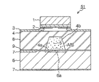
図1は本発明の第1の実施形態に係る原子発振器の構成を示す断面図である。この原子発振器50は、半導体基板上に形成された受光部6aを有する受光素子(PD:Photodiode)6と、受光素子6上に積層され、受光部6aの上部に開口部8aを有する空洞8bが形成されたセル層8と、空洞8bに封入された気体状のアルカリ金属原子5と、開口部8aを閉止するカバーガラス(透明部材)4と、カバーガラス4を介してアルカリ金属原子5に共鳴光を出射する発光素子(VCSEL:Vertical Cavity Surface Emitting Laser(垂直共振器面発光レーザー))1と、を備えて構成されている。尚、受光素子(PD)6には電極7が備えられ、カバーガラス4上には発光素子1用の電極3が形成されている。そして発光素子1のバンプ2を介して電極3と接続される。
即ち、本発明では、まず半導体基板上に受光部6aを有する受光素子6を形成する。そして、更にその上にセル層8を積層して、エッチングにより受光部6aの上部に開口部8aを有する空洞8bを形成する。このセル層8が搭載された状態の構造体をアルカリ金属原子の雰囲気内に置くことにより、空洞8bにアルカリ金属原子5が充満する。その状態で開口部8aをカバーガラス4にて閉止して、カバーガラス4とセル層8とで凹部を有するキャップを構成する。
そして、カバーガラス4の上面の電極3にバンプ2により発光素子6を電極3に接続する。
尚、複数の原子発振器を効率的に形成するためにはバッチ処理工程を採用することが望ましい。
即ち、複数の受光部6aを形成したウエハー状態の半導体基板上にウエハー状態のセル層8を重ねた後、所望の位置に複数の空洞8bを形成し、その後、空洞8b内にアルカリ金属原子を入れた状態のまま開口部8aを閉止するためにウエハー状態のセル層8にウエハー状態のカバーガラス4を重ね合わせて、接合した構造体を用意する。
そして、この構造体に発光素子1を搭載する前または、発光素子1を搭載した後の段階で、構造体を原子発振器毎または発光素子1を搭載する前の状態の原子発振器用のパーツ毎に切断し、固体化する。これにより、容易にモノリシック原子発振器を構成することができる。
なお、半導体基板6に搭載する前に空洞8bを形成したセル層8を用意しても良い。
FIG. 1 is a cross-sectional view showing a configuration of an atomic oscillator according to the first embodiment of the present invention. This atomic oscillator 50 includes a light receiving element (PD: Photodiode) 6 having a
That is, in the present invention, first, the light receiving element 6 having the
Then, the light emitting element 6 is connected to the electrode 3 by the
In order to efficiently form a plurality of atomic oscillators, it is desirable to employ a batch processing process.
That is, after stacking the wafer
And before mounting the light emitting element 1 on this structure, or after mounting the light emitting element 1, the structure is placed for each atomic oscillator or each part for the atomic oscillator in a state before mounting the light emitting element 1. Cut and solidify. Thereby, a monolithic atomic oscillator can be easily configured.
Note that a
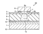
図2は本発明の第2の実施形態に係る原子発振器の構成を示す断面図である。この原子発振器51は、半導体基板上に形成された受光部6aを有する受光素子6(PD)と、受光素子6上に接合され、受光部6aの上部に空洞4bが形成されたカバーガラス(透明部材)4と、空洞4bに封入された気体状のアルカリ金属原子5と、カバーガラス4を介してアルカリ金属原子5に共鳴光を出射する発光素子(VCSEL)1と、を備えて構成されている。尚、受光素子(PD)6には電極7が備えられ、カバーガラス4上には発光素子1用の電極3が形成されている。そして発光素子1のバンプ2を介して電極3と接続される。ここで図1と図2の違いは、図1では半導体基板上にセル層8を搭載した後、空洞8bを形成し、空洞8b内のアルカリ金属原子5を板状のカバーガラス4により封止したものであり、図2では受光素子6とキャップとを予め別体で構成して置き、空洞4bにアルカリ金属原子5
を封入しながら両者を接合するものである(製造方法は後述する)。
即ち、本実施形態では、カバーガラスで開口部を閉止する工程の省略を可能にしている。つまり、半導体基板上に受光部6aを有する受光素子6を形成する。そして、透明材料として例えばガラスに空洞4bを形成したキャップを用意する。その後、アルカリ金属原子の雰囲気内で空洞4bの開口内に受光部6aが収まるようにしてキャップと受光素子6とを重ね合わせて接合することにより、空洞4bにアルカリ金属原子5が充満する。そして、バンプ2により発光素子1を接続する。これにより、エッチングなどの化学処理により受光部6aを傷める心配もなく、容易にモノリシック原子発振器を構成することができる。
なお、図1に示したモノリシック原子発振器の場合においても、受光素子6とキャップとを別体で用意しておき、両者をアルカリ金属原子の雰囲気内で接合しても良い。
FIG. 2 is a sectional view showing a configuration of an atomic oscillator according to the second embodiment of the present invention. This
Both are joined while encapsulating (a manufacturing method will be described later).
That is, in this embodiment, it is possible to omit the step of closing the opening with the cover glass. That is, the light receiving element 6 having the
Even in the case of the monolithic atomic oscillator shown in FIG. 1, the light receiving element 6 and the cap may be prepared separately, and both may be joined in an atmosphere of alkali metal atoms.
図3は本発明の第3の実施形態に係る原子発振器の構成を示す断面図である。この原子発振器52は、半導体基板上に形成された発光部1aを有する発光素子(VCSEL)1と、発光素子1上に積層され、発光部1aの上部に開口部8aを有する空洞8bが形成されたセル層8と、空洞8bに封入された気体状のアルカリ金属原子5と、開口部8aを閉止するカバーガラス(透明部材)4と、カバーガラス4を介してアルカリ金属原子5を透過した共鳴光を受光する受光素子(PD)6と、を備えて構成されている。尚、発光素子(VCSEL)1には電極10が備えられ、カバーガラス4上には受光素子6用の電極3が形成されている。そして受光素子6のバンプ2を介して電極3と接続される。ここで図1と図3の違いは、図1では、受光素子6上に積層したセル層8に空洞8bを形成したが、図3では、発光素子1上に積層したセル層8に空洞8bを形成した。
即ち、本発明では、図1に係る発光素子1と受光素子6の配置を逆転した構成である。即ち、半導体基板上に発光部1aを有する発光素子1を形成する。そして、更にその上にセル層8を積層して、エッチングにより発光部1aの上部に開口部8aを有する空洞8bを形成する。このセル層8をアルカリ金属原子の雰囲気内に置くことにより、空洞8bにアルカリ金属原子5が充満する。その状態で開口部8aをカバーガラス4にて閉止して、バンプ2により受光素子6を接続する。これにより、容易にモノリシック原子発振器を構成することができる。
FIG. 3 is a sectional view showing a configuration of an atomic oscillator according to the third embodiment of the present invention. The atomic oscillator 52 includes a light emitting element (VCSEL) 1 having a light emitting portion 1a formed on a semiconductor substrate, and a
That is, in the present invention, the arrangement of the light emitting element 1 and the light receiving element 6 according to FIG. 1 is reversed. That is, the light emitting element 1 having the light emitting portion 1a is formed on the semiconductor substrate. Further, the
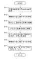
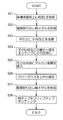
図4は図1の原子発振器の製造工程を説明するフローチャートである。まず、半導体基板上に受光素子6を形成し(S1)、更に電極取出し用の金属膜(以下、単に電極7と呼ぶ)を形成する(S2)。次に、受光素子6上にセル層を積層する(S3)。そして、セル層の一部をエッチングして空洞8bを形成する(S4)。このとき空洞8bは一方に開口部8aを設ける。次に空洞8bに気体状のアルカリ金属原子5を封入し(S5)、カバーガラス4により開口部8aを封止して接合する(S6)。そのカバーガラス4上に電極3を形成する(S7)。最後にアルカリ金属原子5に共鳴光を出射する発光素子1を開口部8a上に実装し、電極3とバンプ2とを接続(フリップチップボンディング)する(S8)。
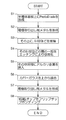
FIG. 4 is a flowchart for explaining a manufacturing process of the atomic oscillator of FIG. First, the light receiving element 6 is formed on the semiconductor substrate (S1), and further, a metal film for electrode extraction (hereinafter simply referred to as the electrode 7) is formed (S2). Next, a cell layer is stacked on the light receiving element 6 (S3). Then, a part of the cell layer is etched to form the
図5は図2の原子発振器の製造工程を説明するフローチャートである。まず、半導体基板上に受光素子6を形成し(S11)、更に電極7を形成する(S12)。次に、受光素子6上に酸化膜9を積層する(S13)。そして、図2のA部にアルカリ金属を積層する(S14)。そして受光素子6と対向する位置に空洞4bを有するキャップをその上から接合する(S15)。そのキャップ上に電極3を形成する(S16)。最後にアルカリ金属原子5に共鳴光を出射する発光素子1をキャップ上に実装し、電極3とバンプ2とを接続(フリップチップボンディング)する(S17)。
FIG. 5 is a flowchart for explaining a manufacturing process of the atomic oscillator of FIG. First, the light receiving element 6 is formed on the semiconductor substrate (S11), and further the
図6は図3の原子発振器の製造工程を説明するフローチャートである。まず、半導体基板上に発光素子1を形成し(S21)、更に電極10を形成する(S22)。次に、発光素子1上にセル層8を積層する(S23)。そして、セル層8の一部をエッチングして空洞8bを形成する(S24)。次に空洞8bに気体状のアルカリ金属原子5を封入し(S25)、カバーガラス4により開口部8aを封止して接合する(S26)。そのカバーガラス4上に電極取3を形成する(S27)。最後に共鳴光を受光する受光素子6を開口部8a上に実装し、電極3とバンプ2とを接続(フリップチップボンディング)する(S28)。
FIG. 6 is a flowchart for explaining a manufacturing process of the atomic oscillator of FIG. First, the light emitting element 1 is formed on the semiconductor substrate (S21), and the
1 発光素子(VCSEL)、1a 発光部、2 バンプ、3 電極、4 カバーガラス、5 アルカリ金属ガス(Csガス)、6 受光素子(PD)、6a 受光部、7 電極、8 セル層、9 酸化皮膜、10 電極、50、51、52 原子発振器 DESCRIPTION OF SYMBOLS 1 Light emitting element (VCSEL), 1a Light emitting part, 2 Bump, 3 electrodes, 4 Cover glass, 5 Alkali metal gas (Cs gas), 6 Light receiving element (PD), 6a Light receiving part, 7 electrode, 8 cell layer, 9 Oxidation Film, 10 electrodes, 50, 51, 52 Atomic oscillator
Claims (8)
空洞を有するセル層と、
前記空洞に封入されている原子と、
前記受光素子とともに前記原子を挟むように配置されていて、前記原子に共鳴光を出射
する発光素子と、
前記受光素子又は前記発光素子上に積層して前記空洞を封止している酸化膜層と、
前記受光素子又は前記発光素子のいずれか一方と前記セル層との間にあるバンプと、
を備えていることを特徴とする原子発振器。 A light receiving element;
A cell layer having a cavity;
Atoms enclosed in the cavity ;
Before SL be arranged so as to sandwich the atom along with the light receiving element, a light emitting element for emitting a resonance light to the atom,
An oxide film layer stacked on the light receiving element or the light emitting element to seal the cavity;
A bump between one of the light receiving element or the light emitting element and the cell layer;
An atomic oscillator characterized by comprising:
1に記載の原子発振器。 The atomic oscillator according to claim 1, wherein the cell layer, the oxide film layer, and the light receiving element are stacked in this order.
1に記載の原子発振器。 The atomic oscillator according to claim 1, wherein the cell layer, the oxide film layer, and the light emitting element are stacked in this order.
透明部材を有することを特徴とする請求項1乃至3の何れか一項に記載の原子発振器。 4. The atomic oscillator according to claim 1, further comprising a transparent member that is disposed so as to sandwich the cavity together with the oxide film layer and seals the cavity. 5.
子発振器。 The atomic oscillator according to any one of claims 1 to 4, wherein the cell layer is a transparent member.
前記受光素子上に酸化膜を積層する第2の工程と、
前記酸化膜上にセル層を積層する第3の工程と、
前記受光部の上部の前記セル層に開口部を有するように空洞を用意する第4の工程と、
前記空洞に気体状のアルカリ金属原子を封入する第5の工程と、
前記開口部を透明部材により封止する第6の工程と、
前記アルカリ金属原子に共鳴光を出射する発光素子を、前記受光素子とともに前記アル
カリ金属原子を挟むように配置し、バンプを介して前記セル層に接続する第7の工程と、
を含むことを特徴とする原子発振器の製造方法。 A first step of preparing a light receiving element having a light receiving portion on a semiconductor substrate;
A second step of laminating an oxide film on the light receiving element;
A third step of laminating a cell layer on the oxide film;
A fourth step of preparing a cavity so as to have an opening in the cell layer above the light receiving portion;
A fifth step of encapsulating gaseous alkali metal atoms in the cavity;
A sixth step of sealing the opening with a transparent member;
A seventh step of arranging a light emitting element that emits resonance light to the alkali metal atom so as to sandwich the alkali metal atom together with the light receiving element, and connecting to the cell layer via a bump ;
A method for manufacturing an atomic oscillator, comprising:
前記受光素子上に酸化膜を積層する第2の工程と、
前記酸化膜上にアルカリ金属を積層する第3の工程と、
前記受光部の上部に空洞を有する透明部材を配置する第4の工程と、
前記受光素子に前記透明部材を接合する第5の工程と、
前記アルカリ金属原子に共鳴光を出射する発光素子を、前記受光素子とともに前記アル
カリ金属原子を挟むように配置し、バンプを介して前記セル層に接続する第6の工程と、
を含むことを特徴とする原子発振器の製造方法。 A first step of preparing a light receiving element having a light receiving portion on a semiconductor substrate;
A second step of laminating an oxide film on the light receiving element;
A third step of laminating an alkali metal on the oxide film;
A fourth step of disposing a transparent member having a cavity above the light receiving portion;
A fifth step of bonding the transparent member to the light receiving element;
A sixth step of arranging a light emitting element that emits resonance light to the alkali metal atom so as to sandwich the alkali metal atom together with the light receiving element, and connecting to the cell layer via a bump ;
A method for manufacturing an atomic oscillator, comprising:
前記発光素子上に酸化膜を積層する第2の工程と、
前記酸化膜上にセル層を積層する第3の工程と、
前記受光部の上部の前記セル層に開口部を有するように空洞を用意する第4の工程と、
前記空洞に気体状のアルカリ金属原子を封入する第5の工程と、
前記開口部を透明部材により封止する第6の工程と、
前記共鳴光が前記アルカリ金属原子を透過した光を受光する受光部を、前記発光素子と
ともに前記アルカリ金属原子を挟むように配置し、バンプを介して前記セル層に接続する第7の工程と、
を含むことを特徴とする原子発振器の製造方法。 A first step of preparing a light emitting element for emitting resonant light on a semiconductor substrate;
A second step of laminating an oxide film on the light emitting element;
A third step of laminating a cell layer on the oxide film;
A fourth step of preparing a cavity so as to have an opening in the cell layer above the light receiving portion;
A fifth step of encapsulating gaseous alkali metal atoms in the cavity;
A sixth step of sealing the opening with a transparent member;
A seventh step in which a light receiving portion that receives the light transmitted through the alkali metal atom by the resonance light is disposed so as to sandwich the alkali metal atom together with the light emitting element, and is connected to the cell layer via a bump ;
A method for manufacturing an atomic oscillator, comprising:
Priority Applications (4)
| Application Number | Priority Date | Filing Date | Title |
|---|---|---|---|
| JP2009273157A JP5504851B2 (en) | 2009-12-01 | 2009-12-01 | Atomic oscillator and manufacturing method |
| EP10192886A EP2333958A1 (en) | 2009-12-01 | 2010-11-29 | Atomic oscillator and manufacturing method |
| US12/956,193 US8710934B2 (en) | 2009-12-01 | 2010-11-30 | Atomic oscillator and manufacturing method |
| CN2010105729819A CN102118165B (en) | 2009-12-01 | 2010-11-30 | Atomic oscillator and manufacturing method |
Applications Claiming Priority (1)
| Application Number | Priority Date | Filing Date | Title |
|---|---|---|---|
| JP2009273157A JP5504851B2 (en) | 2009-12-01 | 2009-12-01 | Atomic oscillator and manufacturing method |
Related Child Applications (1)
| Application Number | Title | Priority Date | Filing Date |
|---|---|---|---|
| JP2010057107A Division JP2011119633A (en) | 2010-03-15 | 2010-03-15 | Method for manufacturing atomic oscillator |
Publications (3)
| Publication Number | Publication Date |
|---|---|
| JP2011119325A JP2011119325A (en) | 2011-06-16 |
| JP2011119325A5 JP2011119325A5 (en) | 2013-01-24 |
| JP5504851B2 true JP5504851B2 (en) | 2014-05-28 |
Family
ID=43502977
Family Applications (1)
| Application Number | Title | Priority Date | Filing Date |
|---|---|---|---|
| JP2009273157A Active JP5504851B2 (en) | 2009-12-01 | 2009-12-01 | Atomic oscillator and manufacturing method |
Country Status (4)
| Country | Link |
|---|---|
| US (1) | US8710934B2 (en) |
| EP (1) | EP2333958A1 (en) |
| JP (1) | JP5504851B2 (en) |
| CN (1) | CN102118165B (en) |
Families Citing this family (14)
| Publication number | Priority date | Publication date | Assignee | Title |
|---|---|---|---|---|
| JP5821439B2 (en) * | 2011-02-16 | 2015-11-24 | セイコーエプソン株式会社 | Gas cell manufacturing method |
| US8624682B2 (en) * | 2011-06-13 | 2014-01-07 | Honeywell International Inc. | Vapor cell atomic clock physics package |
| CN102323738B (en) * | 2011-07-20 | 2014-04-02 | 中国科学院上海微系统与信息技术研究所 | Groove type atomic gas cavity and atomic clock physical system formed by same |
| US9568565B2 (en) * | 2013-07-23 | 2017-02-14 | Texas Instruments Incorporated | Vapor cell structure having cavities connected by channels for micro-fabricated atomic clocks, magnetometers, and other devices |
| JPWO2015019471A1 (en) * | 2013-08-08 | 2017-03-02 | 株式会社日立製作所 | Magnetic field measuring device |
| JP2015118962A (en) * | 2013-12-16 | 2015-06-25 | セイコーエプソン株式会社 | Quantum interference device, atomic oscillator, electronic apparatus and mobile body |
| JP6323650B2 (en) * | 2013-12-20 | 2018-05-16 | セイコーエプソン株式会社 | Surface emitting laser and atomic oscillator |
| US9454135B2 (en) * | 2014-06-19 | 2016-09-27 | Texas Instruments Incorporated | Manufactureable long cell with enhanced sensitivity and good mechanical strength |
| JP6488599B2 (en) * | 2014-09-08 | 2019-03-27 | セイコーエプソン株式会社 | Quantum interferometer, atomic cell manufacturing method, and electronic apparatus |
| US9639062B2 (en) * | 2015-03-30 | 2017-05-02 | Texas Instruments Incorporated | Vapor cell and method for making same |
| US10718661B2 (en) * | 2017-06-14 | 2020-07-21 | Texas Instruments Incorporated | Integrated microfabricated vapor cell sensor with transparent body having two intersecting signal paths |
| US10364144B2 (en) * | 2017-11-17 | 2019-07-30 | Texas Instruments Incorporated | Hermetically sealed package for mm-wave molecular spectroscopy cell |
| US10370760B2 (en) * | 2017-12-15 | 2019-08-06 | Texas Instruments Incorporated | Methods for gas generation in a sealed gas cell cavity |
| US11600581B2 (en) | 2021-04-15 | 2023-03-07 | Texas Instruments Incorporated | Packaged electronic device and multilevel lead frame coupler |
Family Cites Families (8)
| Publication number | Priority date | Publication date | Assignee | Title |
|---|---|---|---|---|
| US6806784B2 (en) * | 2001-07-09 | 2004-10-19 | The National Institute Of Standards And Technology | Miniature frequency standard based on all-optical excitation and a micro-machined containment vessel |
| US6900702B2 (en) | 2002-08-14 | 2005-05-31 | Honeywell International Inc. | MEMS frequency standard for devices such as atomic clock |
| US7400207B2 (en) * | 2004-01-06 | 2008-07-15 | Sarnoff Corporation | Anodically bonded cell, method for making same and systems incorporating same |
| WO2006017345A2 (en) * | 2004-07-13 | 2006-02-16 | The Charles Stark Draper Laboratory, Inc. | Apparatus for suspending a chip-scale device and atomic clock system |
| CN100580584C (en) * | 2005-07-21 | 2010-01-13 | 精工爱普生株式会社 | Portable clock and electronic device |
| US7468637B2 (en) * | 2006-04-19 | 2008-12-23 | Sarnoff Corporation | Batch-fabricated, RF-interrogated, end transition, chip-scale atomic clock |
| US7619485B2 (en) * | 2007-01-31 | 2009-11-17 | Teledyne Scientific & Imaging, Llc | Compact optical assembly for chip-scale atomic clock |
| CN201266923Y (en) * | 2008-09-09 | 2009-07-01 | 北京七维航测科技发展有限公司 | GPS combined time frequency instrument |
-
2009
- 2009-12-01 JP JP2009273157A patent/JP5504851B2/en active Active
-
2010
- 2010-11-29 EP EP10192886A patent/EP2333958A1/en not_active Withdrawn
- 2010-11-30 US US12/956,193 patent/US8710934B2/en active Active
- 2010-11-30 CN CN2010105729819A patent/CN102118165B/en active Active
Also Published As
| Publication number | Publication date |
|---|---|
| CN102118165B (en) | 2013-11-27 |
| JP2011119325A (en) | 2011-06-16 |
| EP2333958A1 (en) | 2011-06-15 |
| US20110128082A1 (en) | 2011-06-02 |
| US8710934B2 (en) | 2014-04-29 |
| CN102118165A (en) | 2011-07-06 |
Similar Documents
| Publication | Publication Date | Title |
|---|---|---|
| JP5504851B2 (en) | Atomic oscillator and manufacturing method | |
| JP2011119325A5 (en) | ||
| US8991022B2 (en) | Method for manufacturing piezoelectric resonator device | |
| JP4707725B2 (en) | Package type piezoelectric vibrator and manufacturing method of package type piezoelectric vibrator | |
| JP4988799B2 (en) | Piezoelectric vibration device and method for manufacturing piezoelectric vibration device | |
| JP4938124B2 (en) | Crystal device | |
| JP4864152B2 (en) | Surface mount crystal unit | |
| CN107615648B (en) | Piezoelectric vibration device | |
| US11342897B2 (en) | Piezoelectric resonator device and method for manufacturing piezoelectric resonator device | |
| JP6780718B2 (en) | Piezoelectric vibration device | |
| JP2011119633A (en) | Method for manufacturing atomic oscillator | |
| JP2010130400A (en) | Piezoelectric vibration device | |
| JP2007251601A (en) | Small piezoelectric oscillator, and manufacturing method of small piezoelectric oscillator | |
| JP2007235289A (en) | Piezoelectric oscillator | |
| KR20060116054A (en) | Ceramic package of crystal oscillator | |
| JP2013026506A (en) | Electronic component storing package and electronic apparatus | |
| JP2013009280A (en) | Lid for piezoelectric vibration device and piezoelectric vibration device using the same | |
| JP2008182468A (en) | Manufacturing method of piezoelectric vibration device | |
| JP2009088699A (en) | Manufacturing method of piezoelectric device and piezoelectric device | |
| US20230291381A1 (en) | Vibrator device and method for manufacturing vibrator device | |
| JP4780700B2 (en) | ELECTRONIC PROTECTION ELECTRONIC COMPONENT AND MANUFACTURING METHOD THEREOF | |
| JP2010098340A (en) | Piezoelectric vibrator, piezoelectric oscillator, and method of manufacturing piezoelectric oscillator | |
| JP2023108260A (en) | vibration device | |
| JP2013120762A (en) | Lid, package, electronic component, and manufacturing method of package | |
| JP6077386B2 (en) | Method for manufacturing piezoelectric vibrator |
Legal Events
| Date | Code | Title | Description |
|---|---|---|---|
| A521 | Request for written amendment filed |
Free format text: JAPANESE INTERMEDIATE CODE: A523 Effective date: 20121203 |
|
| A621 | Written request for application examination |
Free format text: JAPANESE INTERMEDIATE CODE: A621 Effective date: 20121203 |
|
| A131 | Notification of reasons for refusal |
Free format text: JAPANESE INTERMEDIATE CODE: A131 Effective date: 20130910 |
|
| TRDD | Decision of grant or rejection written | ||
| A01 | Written decision to grant a patent or to grant a registration (utility model) |
Free format text: JAPANESE INTERMEDIATE CODE: A01 Effective date: 20140218 |
|
| A61 | First payment of annual fees (during grant procedure) |
Free format text: JAPANESE INTERMEDIATE CODE: A61 Effective date: 20140303 |
|
| R150 | Certificate of patent or registration of utility model |
Ref document number: 5504851 Country of ref document: JP Free format text: JAPANESE INTERMEDIATE CODE: R150 |
|
| S531 | Written request for registration of change of domicile |
Free format text: JAPANESE INTERMEDIATE CODE: R313531 |
|
| R350 | Written notification of registration of transfer |
Free format text: JAPANESE INTERMEDIATE CODE: R350 |
|
| S111 | Request for change of ownership or part of ownership |
Free format text: JAPANESE INTERMEDIATE CODE: R313113 |
|
| R350 | Written notification of registration of transfer |
Free format text: JAPANESE INTERMEDIATE CODE: R350 |
|
| R250 | Receipt of annual fees |
Free format text: JAPANESE INTERMEDIATE CODE: R250 |