EP2328313B1 - Method and apparatus for demodulating differential binary phase shift keying modulated signals - Google Patents
Method and apparatus for demodulating differential binary phase shift keying modulated signals Download PDFInfo
- Publication number
- EP2328313B1 EP2328313B1 EP20090177529 EP09177529A EP2328313B1 EP 2328313 B1 EP2328313 B1 EP 2328313B1 EP 20090177529 EP20090177529 EP 20090177529 EP 09177529 A EP09177529 A EP 09177529A EP 2328313 B1 EP2328313 B1 EP 2328313B1
- Authority
- EP
- European Patent Office
- Prior art keywords
- phase component
- quadrature
- phase
- digital
- bit
- Prior art date
- Legal status (The legal status is an assumption and is not a legal conclusion. Google has not performed a legal analysis and makes no representation as to the accuracy of the status listed.)
- Active
Links
Images

Classifications
-
- H—ELECTRICITY
- H04—ELECTRIC COMMUNICATION TECHNIQUE
- H04L—TRANSMISSION OF DIGITAL INFORMATION, e.g. TELEGRAPHIC COMMUNICATION
- H04L27/00—Modulated-carrier systems
- H04L27/18—Phase-modulated carrier systems, i.e. using phase-shift keying
- H04L27/22—Demodulator circuits; Receiver circuits
- H04L27/233—Demodulator circuits; Receiver circuits using non-coherent demodulation
- H04L27/2331—Demodulator circuits; Receiver circuits using non-coherent demodulation wherein the received signal is demodulated using one or more delayed versions of itself
Definitions
- the present invention relates to a method, apparatus and computer program product for demodulating a differential binary phase shift keying (DBPSK) signal.
- DBPSK differential binary phase shift keying
- DPSK is a digital modulation technique that can be used to encode information in a signal prior to transmitting the signal to one or more receivers.
- information is carried by a transition between distinct digital states rather than absolute digital states.
- Specific DPSK modulation techniques include DBPSK and differential quadrature phase shift keying (DQPSK).
- the phase of a constant amplitude carrier signal shifts between two positions, such as 0° and 180°.
- two distinct digital states are provided, for example, a binary "0" state at 0° and a binary "1" state at 180°.
- Information is differentially encoded in the transition from one state to the next, and/or a lack of such a transition.
- the receiver only needs to identify the relative phase shift between two adjacent bits to identify the information contained in a differentially encoded signal. This tends to simplify the design of the receiver.
- a differential coding the phase of a preceding symbol is multiplied by the phase of a current symbol.
- a typical receiver for a DBPSK signal may comprise an analog radio frequency (RF) front end in which the modulated received signal is converted from the RF band to the lower base band.
- the obtained base band signal is digitized by an analog-to-digital (A/D) converter and then processed further.
- A/D analog-to-digital
- Differential coding can be advantageously used if no phase synchronisation is implemented between a transmitter and a receiver.
- determination of the phase difference requires sufficient resolution of the applied A/D conversion.
- the DBPSK signal is quantized at only 1 bit, demodulation is no longer possible at a phase difference of about 90° or 270° between the transmitter and the receiver.
- DBPSK demodulation involves a problem in that either an analog determination of the phase difference at correspondingly higher circuit complexity or an A/D converter with sufficient resolution are required.
- Such A/D convert-er may be disadvantageous for systems with high data rates (e.g. >1Gbit/s) due to the relatively higher power consumption and circuit complexity, and it is therefore of limited use for cheap or battery power modules.
- the document US 6,381,288 B1 discloses a method and apparatus for recovering data from a DBPSK signal, wherein the receiver demodulates the DBPSK signal by a quadrature demodulator into separate in-phase and quadrature-phase components which are converted into two digital signals using 2-bit A/D converters. Samples of these digital signals are then decoded according to a maximum likelihood criteria algorithm and decisions are made based on the signal constellation which identifies the original data transmitted.
- US 2007/0018717 A1 discloses an evaluation device, which reproduces I- and Q-components by using channel estimation, wherein modulated data is reproduced from the I- and Q-components.
- Wu describes in Milcom 98.proceedings, vol. 3, 18. October 1998, pages 730-735 a BPSK demodulator with a 1-bit A/D front-end, wherein the received signal is converted by a 1-bit A/D converter prior to the generation of the I- and Q-components.
- the maximum likelihood estimate is calculated separately for both I- and Q-components, while the value of the received BPSK signal is decided based on an addition of the process I- and Q-components.
- US 6,381,288 B1 describes a demodulator for a DBPSK signal, wherein the I- and Q-components are separately sampled and than encoded according to a maximum likelihood criteria algorithm.
- the document EP 1 791 312 A2 discloses a method for demodulating a DBPSK signal in accordance with the preamble of claim 1.
- a separate 1-bit A/D conversion and subsequent demodulation processing is applied for each of the in-phase and quadrature-phase components, so that complex A/D converters are no longer required and the 1-bit quantized demodulation values can be used as input information to a maximum likelihood decoding operation of at least one decoder or a checksum calculation.
- the in-phase and quadrature-phase components allows conversion of the differentially decoded values to softbit values which include reliability considerations. Additionally, in embodiments of the method, the in-phase and quadrature-phase components can be used separately for deciding on the value of the DBPSK input signal based on a determined error rate or maximum likelihood decoding (such as for example Viterbi decoding).
- the DBPSK signal is a received channel-coded signal, wherein channel coding may is based on a convolution code.
- the decision on the value of the DBPSK signal may be achieved by applying maximum likelihood decoding with softbits as input metrics, wherein the softbits are generated by adding the processed in-phase component and the processed quadrature-phase component.
- the decision on the value of the DBPSK signal may be performed by separately applying maximum likelihood decoding to the processed in-phase component and the processed quadrature-phase component, and deciding based on checksum calculations about validity of the obtained decoding results.
- the checksum calculations may be performed for partial blocks of the processed in-phase and quadrature-phase components and deciding about the validity based on the partial blocks.
- the decision on the value of the DBPSK signal may be performed by separately applying maximum likelihood decoding to the processed in-phase component, to the processed quadrature-phase component, and to a sum of the processed in-phase component and the processed quadrature-phase component, and deciding based on checksum calculations about validity of the obtained decoding results.
- the checksum calculations may be performed for partial blocks.
- the decision on the value of the DBPSK signal may be performed by separately applying a block code processing to partial blocks of the in-phase component and the quadrature-phase component and by deciding based on checksum calculations or a corrected number of errors about validity of decoding results.
- the decision about validity may be performed after each partial block.
- the checksum calculations may be based on a cyclic redundancy code.
- the claimed apparatus may be represented by a semiconductor chip, a chip set, or a hardware module comprising such chip or chip set. This, however, does not exclude the possibility that a functionality of an apparatus or module, instead of being hardware implemented, be implemented as software in a software module such as a computer program or a computer program product comprising executable software code portions for execution or being run on a processor.
- the embodiments are applicable to any receiver in any communication system or any combination of different communication systems in which DBPSK signals are transmitted.
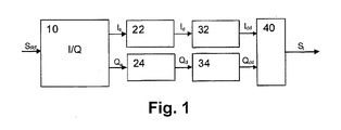
- Fig. 1 shows a schematic block diagram of a demodulation circuit or procedure according to various embodiments.
- a DBPSK signal S RF in the radio frequency (RF) domain or intermediate frequency (IF) domain as received from an RF front end of a receiver is supplied to a quadrature demodulator 10 configured to generate an analog in-phase component I a and an analog quadrature-phase component Q a of the received DBPSK signal S RF .
- the two demodulated components I a and Q a are supplied to separate I and Q branches where they are separately processed.
- the analog in-phase component I a is supplied to a 1-bit A/D converter 22, which may be implemented as a simple comparator circuit, to generate a digital in-phase component I d which could represent for example binary values, such as "1" or "0". Of course, other coding options can be used for the binary values.
- the 1-bit content may as well be interpreted as "+1" or "-1” or the like.
- This digital in-phase component I d is then supplied to a differential decoder 32 where two subsequent symbols of the digital in-phase component I d are processed to obtain a decoded digital in-phase component I dd .
- the analog quadrature-phase component Q a is A/D converted in a 1-bit A/D converter 24, which may also be implemented as a simple comparator circuit, to generate a digital quadrature-phase component Q d which is then supplied to a differential decoder 34 where two successive values of the digital quadrature-phase component Q d are processed to obtain a decoded digital quadrature-phase component Q dd .
- the two separate decoded digital in-phase and quadrature-phase components I dd and Q dd are supplied to a decision unit or functionality 40 which decides on the value of the received DBPSK signal S RF based on maximum likelihood decoding of each component or a combination of the two components and/or a checksum calculation based on an error code provided in the received DBPSK signal S RF .
- the output signal of the decision unit 40 is a binary information value S i which corresponds to the information which has been DBPSK-modulated on the carrier of the received DBPSK signal.
- the use of the simple 1-bit A/D converters 22 and 24 enables a simple structure and easy processing in the decision unit based on maximum likelihood decoding and checksum calculation, since only one binary value has to be processed for every symbol or value. This is advantageous for example in high speed and high frequency applications which may be used in wireless communication systems, for example.
- a suitable combination of the two 1-bit quantized and decoded input values I dd and Q dd of the decision unit 40 could be used for example as softbits for a maximum likelihood decoding such as for example a soft decision Viterby decoding.
- the softbits also contain information about the reliability of each received symbol.
- the decision unit 40 may incorporate a plurality of decoding units or functions, wherein a selection of one of the decoded data streams is performed based on a determined error rate.
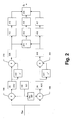
- Fig. 2 shows a more detailed block or flow diagram of a DBPSK decoding approach according to a first embodiment.
- the quadrature demodulator 10 can be implemented by using two multipliers 106, 108 which multiply an oscillation signal generated by a local oscillator (LO) 102 with the received DBPSK signal S RF , wherein the lower multiplier 108 is supplied with a 90° phase-shifted version of the oscillation signal to obtain the analog quadrature-phase component.
- the phase shift is achieved by a phase shifting element or function 104.
- the multiplier in the upper branch or I branch generates the in-phase component which is separately processed in the I branch, while the quadrature-phase component is separately processed in the lower branch or Q branch.
- the frequency of the oscillation signal of the local oscillator 102 depends on the carrier frequency of the received DBPSK signal S RF (e.g. RF frequency range or IF frequency range) to obtain a down conversion of the in-phase and quadrature-phase components to base band level.
- S RF e.g. RF frequency range or IF frequency range
- the obtained analog in-phase and quadrature phase components are supplied to respective 1-bit A/D converters (ADC) 22, 24 which may be implemented based on simple comparator circuits with a threshold level for distinguishing between the binary values "0" and "1". Accordingly, the output of the A/D converters 22, 24 corresponds to a sequence of binary values which correspond to the binary values signaled by the transition or non-transition between the two phases of the DBPSK signal S RF .
- ADC 1-bit A/D converters
- the respective digital in-phase and quadrature-phase components are supplied to respective differential decoders which comprise respective combiners 324, 344, which may be implemented as multipliers or logic elements (e.g.
- delay circuits 322, 342 may be implemented as storing elements for temporarily storing a bit value of the digitized in-phase and quadrature-phase components, respectively.
- the output signals of the respective combiners 324, 344 may be supplied to optional deinterleaver circuits or functions 326, 346 which are configured to remove an interleaving structure introduced at the transmission side to improve transmission reliability.
- the decoded digital in-phase and quadrature-phase components are then processed in three different maximum likelihood decoding functions or units 412, 414, 416 and subsequent checksum calculation units or functions 413, 415, 417 to provide different checksum results to a selection unit or function 418.
- the maximum likelihood decoding units 412, 416 of the I branch and Q branch may be configured to apply a hard-decision Viterbi decoding procedure, where the bit sequence of the digital decoded in-phase component and quadrature-phase component are respectively used as input signals.
- the decoded bit pattern is subjected to a checksum calculation where a string of data bits are taken and added together and compared with a predetermined sum or a sum received from the transmitter to detect bit errors.
- the bits of the digital decoded in-phase and quadrature-phase components are combined in a combination unit or function 411 and are then used as softbits input to a soft-decision Viterbi procedure of the maximum likelihood decoding unit 414.
- the combination of the in-phase and quadrature-phase components provides an additional information about the reliability of each received symbol depending on whether the bit values of the digital decoded in-phase and quadrature-phase components are equal or not.
- the output values of the soft-decision Viterbi procedure are supplied to the checksum calculation unit 415 which calculates a checksum. Based on the checksum calculations of the three branches, the selection unit 418 decides about the binary value of the demodulated information S i .
- the checksum protection may be achieved by separating the transmitted data stream into partial blocks protected by a respective checksum.
- the data stream is processed at the transmitter by a convolution coding.
- the obtained I and Q branches are quantized by one bit.
- a phase difference is separately obtained in both branches at the output of the respective combiners 324, 344 and the channel code is decoded in the respective maximum likelihood decoding units 412, 416.
- the selection unit 418 may then select a partial block with matching checksum.
- a third maximum likelihood decoding is applied, wherein the metrics of the I and Q branches are combined to obtain softbits as input metric to the soft-decision Viterbi procedure.
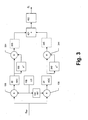
- Fig. 3 shows a more detailed block diagram of a decoding approach according to a second embodiment, where the decision about the value of the received DBPSK signal is not achieved based on checksums, and only one maximum likelihood decoding unit 422 is used to which a combination of the metrics of the I and Q branch is used as softbit input for a soft-decision Viterbi procedure of the maximum likelihood decoding unit 422.
- the soft-decision Viterbi procedure provides a value of the modulated information S i of the received DBPSK signal S RF .
- Fig. 4 shows a more detailed block diagram of a demodulating approach according to a third embodiment.
- the decision unit 40 now processes the data stream of the I and Q branches based on respective maximum likelihood decoding procedures in maximum likelihood decoding units or functions 432, 436 followed by respective checksum calculation units or functions 433, 437 without a combined third branch.
- the two maximum likelihood decoding units 432, 436 can be based on hard-decision Viterbi decoding procedures for obtaining a channel-decoded bit sequence used for subsequent checksum calculation.
- a final selection unit or function 438 is then provided to select the partial block with matching checksum as base band modulation information S i .
- a block code could be used for channel coding, which is applied to the partial blocks enhanced by the checksum. Then, the decoding can be performed in different branches, wherein the checksum as well as the corrected number of errors can be used for selecting a valid partial block in the final selection unit.
- a control processor or computer device comprises a processing unit which may be any processor or processing device with a control unit which performs control based on software routines of a control program stored in a memory.
- Program code instructions are fetched from the memory and are loaded to the control unit of the processing unit in order to perform the processing steps of the above functionalities described in connection with Figs. 2 to 4 .
- These processing steps may be performed on the basis of input data and may generate output data, wherein the input data may correspond to the received DBPSK signal S RF or any signal between the blocks of Fig. 2 to 4 .
- the output data may correspond to the obtained base band modulation information S i which reflects the demodulated data or any signal between the blocks of Fig. 2 to 4 for further processing.
- some or all of the proposed demodulation structures according to the first to third embodiment can be implemented as software routines or programs controlling a processor or computer device to perform the processing steps of the above functionalities.
- a method, apparatus and computer program product for demodulating a DBPSK signal have been described, wherein an in-phase component and a quadrature-phase component are generated from the DBPSK signal, and the in-phase component and quadrature-phase component are separately processed by applying 1-bit analog-to-digital conversion and subsequent differential decoding. Then, a decision on the value of the DBPSK signal is based on a combined consideration of at least one of a maximum likelihood decoding and checksum calculation of the processed in-phase and quadrature-phase components.
- the present invention is not restricted to the embodiments described above, but can be implemented in any demodulation circuit or procedure where maximum likelihood decoding can be used for decoding 1-bit quantized in-phase and quadrature-phase components.
Landscapes
- Engineering & Computer Science (AREA)
- Computer Networks & Wireless Communication (AREA)
- Signal Processing (AREA)
- Digital Transmission Methods That Use Modulated Carrier Waves (AREA)
- Error Detection And Correction (AREA)
Description
- The present invention relates to a method, apparatus and computer program product for demodulating a differential binary phase shift keying (DBPSK) signal.
- DPSK is a digital modulation technique that can be used to encode information in a signal prior to transmitting the signal to one or more receivers. In a DPSK modulated signal, information is carried by a transition between distinct digital states rather than absolute digital states. Specific DPSK modulation techniques include DBPSK and differential quadrature phase shift keying (DQPSK).
- In DBPSK modulation, the phase of a constant amplitude carrier signal shifts between two positions, such as 0° and 180°. As such, two distinct digital states are provided, for example, a binary "0" state at 0° and a binary "1" state at 180°. Information is differentially encoded in the transition from one state to the next, and/or a lack of such a transition. As such, there is no need to recover or track the carrier signal within the receiver, as required quired in a receiver that is configured to demodulate conventional phase shift keyed signals. Instead, the receiver only needs to identify the relative phase shift between two adjacent bits to identify the information contained in a differentially encoded signal. This tends to simplify the design of the receiver. Thus, in case of a differential coding the phase of a preceding symbol is multiplied by the phase of a current symbol.
- A typical receiver for a DBPSK signal may comprise an analog radio frequency (RF) front end in which the modulated received signal is converted from the RF band to the lower base band. The obtained base band signal is digitized by an analog-to-digital (A/D) converter and then processed further. However, it is possible, as well, to demodulate the differentially coded signal in the analog domain by providing additional circuitry or processing steps.
- Differential coding can be advantageously used if no phase synchronisation is implemented between a transmitter and a receiver. However, determination of the phase difference requires sufficient resolution of the applied A/D conversion. If the DBPSK signal is quantized at only 1 bit, demodulation is no longer possible at a phase difference of about 90° or 270° between the transmitter and the receiver. Thus, DBPSK demodulation involves a problem in that either an analog determination of the phase difference at correspondingly higher circuit complexity or an A/D converter with sufficient resolution are required. Such A/D convert-er may be disadvantageous for systems with high data rates (e.g. >1Gbit/s) due to the relatively higher power consumption and circuit complexity, and it is therefore of limited use for cheap or battery power modules.
- The document
US 6,381,288 B1 discloses a method and apparatus for recovering data from a DBPSK signal, wherein the receiver demodulates the DBPSK signal by a quadrature demodulator into separate in-phase and quadrature-phase components which are converted into two digital signals using 2-bit A/D converters. Samples of these digital signals are then decoded according to a maximum likelihood criteria algorithm and decisions are made based on the signal constellation which identifies the original data transmitted. -
US 2007/0018717 A1 discloses an evaluation device, which reproduces I- and Q-components by using channel estimation, wherein modulated data is reproduced from the I- and Q-components. - Wu describes in Milcom 98.proceedings, vol. 3, 18. October 1998, pages 730-735 a BPSK demodulator with a 1-bit A/D front-end, wherein the received signal is converted by a 1-bit A/D converter prior to the generation of the I- and Q-components. The maximum likelihood estimate is calculated separately for both I- and Q-components, while the value of the received BPSK signal is decided based on an addition of the process I- and Q-components.
-
US 2007/024477 A1 and Qing et al., IEEE 16th International Symposium on Personal, Indoor and Mobile Radio Communications, Berlin 11-14. September 2005, vol. 4, pages 2586-2590 disclose demodulator solutions, where the received signal is first digitized via a hard limiter and than separated into I- and Q-components. -
US 6,381,288 B1 describes a demodulator for a DBPSK signal, wherein the I- and Q-components are separately sampled and than encoded according to a maximum likelihood criteria algorithm. - The
document EP 1 791 312 A2 discloses a method for demodulating a DBPSK signal in accordance with the preamble ofclaim 1. - It is therefore an object of the present invention to provide a simplified DBPSK demodulation technique with less circuit complexity and power consumption.
- This object is achieved by a method for demodulating a DBPSK signalin accordance with
claim 1. - Additionally, the above object is achieved by an apparatus for demodulating a DBPSK signal in accordance with claim 5.
- Furthermore, the above object is achieved by computer program product comprising code means for carrying out the method steps of
claim 1 when run on a computing device. - Accordingly, a separate 1-bit A/D conversion and subsequent demodulation processing is applied for each of the in-phase and quadrature-phase components, so that complex A/D converters are no longer required and the 1-bit quantized demodulation values can be used as input information to a maximum likelihood decoding operation of at least one decoder or a checksum calculation.
- The combined consideration of the in-phase and quadrature-phase components allows conversion of the differentially decoded values to softbit values which include reliability considerations. Additionally, in embodiments of the method, the in-phase and quadrature-phase components can be used separately for deciding on the value of the DBPSK input signal based on a determined error rate or maximum likelihood decoding (such as for example Viterbi decoding).
- The DBPSK signal is a received channel-coded signal, wherein channel coding may is based on a convolution code.
- According to a first aspect, the decision on the value of the DBPSK signal may be achieved by applying maximum likelihood decoding with softbits as input metrics, wherein the softbits are generated by adding the processed in-phase component and the processed quadrature-phase component.
- According to a second aspect, the decision on the value of the DBPSK signal may be performed by separately applying maximum likelihood decoding to the processed in-phase component and the processed quadrature-phase component, and deciding based on checksum calculations about validity of the obtained decoding results. According to a specific implementation, the checksum calculations may be performed for partial blocks of the processed in-phase and quadrature-phase components and deciding about the validity based on the partial blocks.
- According to a third aspect, the decision on the value of the DBPSK signal may be performed by separately applying maximum likelihood decoding to the processed in-phase component, to the processed quadrature-phase component, and to a sum of the processed in-phase component and the processed quadrature-phase component, and deciding based on checksum calculations about validity of the obtained decoding results. In a specific implementation example, the checksum calculations may be performed for partial blocks.
- According to a fourth aspect, the decision on the value of the DBPSK signal may be performed by separately applying a block code processing to partial blocks of the in-phase component and the quadrature-phase component and by deciding based on checksum calculations or a corrected number of errors about validity of decoding results.
- In a specific implementation example, the decision about validity may be performed after each partial block.
- Furthermore, in the above second to fourth aspects, the checksum calculations may be based on a cyclic redundancy code.
- The claimed apparatus may be represented by a semiconductor chip, a chip set, or a hardware module comprising such chip or chip set. This, however, does not exclude the possibility that a functionality of an apparatus or module, instead of being hardware implemented, be implemented as software in a software module such as a computer program or a computer program product comprising executable software code portions for execution or being run on a processor.
- The present invention will now be described on the basis of embodiments with reference to the accompanying drawings in which:
-
Fig. 1 shows a schematic block diagram of a demodulation apparatus according to various embodiments; -
Fig. 2 shows a more detailed block diagram of a demodulation apparatus according to a first embodiment; -
Fig. 3 shows a more detailed block diagram of a demodulation apparatus according to a second embodiment; and -
Fig. 4 shows a more detailed block diagram of a demodulation apparatus according to a third embodiment. - Exemplary embodiments of the present invention will now be described. Indeed, the invention may be embodied in many different forms and should not be constructed as limited to the embodiments set forth herein. Although the specification may refer to "an", "one" or "some" embodiment(s) in several locations, this does not necessarily mean that each such reference is to the same embodiment(s), or that the feature only applies to a single embodiment. Single features of different embodiments may also be combined to provide other embodiments. Like reference numerals refer to like elements throughout the following specification. Additionally, it is to be noted that the blocks described in the following block diagrams may be implemented as hardware circuits, software modules or a combination of both. Thus, the following block diagrams can be seen as illustrations of hardware devices or functional procedures for carrying out the proposed demodulation.
- The embodiments are applicable to any receiver in any communication system or any combination of different communication systems in which DBPSK signals are transmitted.
-
Fig. 1 shows a schematic block diagram of a demodulation circuit or procedure according to various embodiments. A DBPSK signal SRF in the radio frequency (RF) domain or intermediate frequency (IF) domain as received from an RF front end of a receiver is supplied to aquadrature demodulator 10 configured to generate an analog in-phase component Ia and an analog quadrature-phase component Qa of the received DBPSK signal SRF. The two demodulated components Ia and Qa are supplied to separate I and Q branches where they are separately processed. More specifically, the analog in-phase component Ia is supplied to a 1-bit A/D converter 22, which may be implemented as a simple comparator circuit, to generate a digital in-phase component Id which could represent for example binary values, such as "1" or "0". Of course, other coding options can be used for the binary values. The 1-bit content may as well be interpreted as "+1" or "-1" or the like. This digital in-phase component Id is then supplied to adifferential decoder 32 where two subsequent symbols of the digital in-phase component Id are processed to obtain a decoded digital in-phase component Idd. - Similarly, in the lower Q branch the analog quadrature-phase component Qa is A/D converted in a 1-bit A/
D converter 24, which may also be implemented as a simple comparator circuit, to generate a digital quadrature-phase component Qd which is then supplied to adifferential decoder 34 where two successive values of the digital quadrature-phase component Qd are processed to obtain a decoded digital quadrature-phase component Qdd. The two separate decoded digital in-phase and quadrature-phase components Idd and Qdd are supplied to a decision unit orfunctionality 40 which decides on the value of the received DBPSK signal SRF based on maximum likelihood decoding of each component or a combination of the two components and/or a checksum calculation based on an error code provided in the received DBPSK signal SRF. The output signal of thedecision unit 40 is a binary information value Si which corresponds to the information which has been DBPSK-modulated on the carrier of the received DBPSK signal. - The use of the simple 1-bit A/
D converters - A suitable combination of the two 1-bit quantized and decoded input values Idd and Qdd of the
decision unit 40 could be used for example as softbits for a maximum likelihood decoding such as for example a soft decision Viterby decoding. In this case, the softbits also contain information about the reliability of each received symbol. As an alternative, thedecision unit 40 may incorporate a plurality of decoding units or functions, wherein a selection of one of the decoded data streams is performed based on a determined error rate. -
Fig. 2 shows a more detailed block or flow diagram of a DBPSK decoding approach according to a first embodiment. - As can be gathered from
Fig. 2 , thequadrature demodulator 10 can be implemented by using twomultipliers lower multiplier 108 is supplied with a 90° phase-shifted version of the oscillation signal to obtain the analog quadrature-phase component. The phase shift is achieved by a phase shifting element or function 104. The multiplier in the upper branch or I branch generates the in-phase component which is separately processed in the I branch, while the quadrature-phase component is separately processed in the lower branch or Q branch. - The frequency of the oscillation signal of the
local oscillator 102 depends on the carrier frequency of the received DBPSK signal SRF (e.g. RF frequency range or IF frequency range) to obtain a down conversion of the in-phase and quadrature-phase components to base band level. - The obtained analog in-phase and quadrature phase components are supplied to respective 1-bit A/D converters (ADC) 22, 24 which may be implemented based on simple comparator circuits with a threshold level for distinguishing between the binary values "0" and "1". Accordingly, the output of the A/
D converters respective combiners functions respective combiner delay circuits - The output signals of the
respective combiners - The decoded digital in-phase and quadrature-phase components are then processed in three different maximum likelihood decoding functions or
units functions - More specifically, the maximum
likelihood decoding units checksum calculation units likelihood decoding unit 414. In this case, the combination of the in-phase and quadrature-phase components provides an additional information about the reliability of each received symbol depending on whether the bit values of the digital decoded in-phase and quadrature-phase components are equal or not. The output values of the soft-decision Viterbi procedure are supplied to thechecksum calculation unit 415 which calculates a checksum. Based on the checksum calculations of the three branches, theselection unit 418 decides about the binary value of the demodulated information Si. - The checksum protection may be achieved by separating the transmitted data stream into partial blocks protected by a respective checksum. In this case, the data stream is processed at the transmitter by a convolution coding. At the demodulation circuit of
Fig. 2 , which is provided at the receiver side, the obtained I and Q branches are quantized by one bit. A phase difference is separately obtained in both branches at the output of therespective combiners likelihood decoding units selection unit 418 may then select a partial block with matching checksum. In the third branch, a third maximum likelihood decoding is applied, wherein the metrics of the I and Q branches are combined to obtain softbits as input metric to the soft-decision Viterbi procedure. -
Fig. 3 shows a more detailed block diagram of a decoding approach according to a second embodiment, where the decision about the value of the received DBPSK signal is not achieved based on checksums, and only one maximumlikelihood decoding unit 422 is used to which a combination of the metrics of the I and Q branch is used as softbit input for a soft-decision Viterbi procedure of the maximumlikelihood decoding unit 422. The soft-decision Viterbi procedure provides a value of the modulated information Si of the received DBPSK signal SRF. -
Fig. 4 shows a more detailed block diagram of a demodulating approach according to a third embodiment. In contrast to the first and second embodiment, thedecision unit 40 now processes the data stream of the I and Q branches based on respective maximum likelihood decoding procedures in maximum likelihood decoding units orfunctions functions likelihood decoding units - It is noted that the above block diagrams of
Figs. 2 to 4 only serve to provide a schematic overview of relevant functionalities, while usual or optional functionalities, such as low pass filters or pulse shaping functions have been omitted for reasons of brevity. - As an alternative to the above first to third embodiments, a block code could be used for channel coding, which is applied to the partial blocks enhanced by the checksum. Then, the decoding can be performed in different branches, wherein the checksum as well as the corrected number of errors can be used for selecting a valid partial block in the final selection unit.
- As already mentioned, all or some of the blocks of
Figs. 2 to 4 can be interpreted as software routines of a software-based implementation of the proposed demodulation device or apparatus. In this case, a control processor or computer device comprises a processing unit which may be any processor or processing device with a control unit which performs control based on software routines of a control program stored in a memory. Program code instructions are fetched from the memory and are loaded to the control unit of the processing unit in order to perform the processing steps of the above functionalities described in connection withFigs. 2 to 4 . These processing steps may be performed on the basis of input data and may generate output data, wherein the input data may correspond to the received DBPSK signal SRF or any signal between the blocks ofFig. 2 to 4 . The output data may correspond to the obtained base band modulation information Si which reflects the demodulated data or any signal between the blocks ofFig. 2 to 4 for further processing. Thus, some or all of the proposed demodulation structures according to the first to third embodiment can be implemented as software routines or programs controlling a processor or computer device to perform the processing steps of the above functionalities. - To summarize, a method, apparatus and computer program product for demodulating a DBPSK signal have been described, wherein an in-phase component and a quadrature-phase component are generated from the DBPSK signal, and the in-phase component and quadrature-phase component are separately processed by applying 1-bit analog-to-digital conversion and subsequent differential decoding. Then, a decision on the value of the DBPSK signal is based on a combined consideration of at least one of a maximum likelihood decoding and checksum calculation of the processed in-phase and quadrature-phase components.
- It is noted that the present invention is not restricted to the embodiments described above, but can be implemented in any demodulation circuit or procedure where maximum likelihood decoding can be used for decoding 1-bit quantized in-phase and quadrature-phase components.
Claims (6)
- A method for demodulating a differential binary phase shift keying DBPSK signal, said method comprising the steps of:- receiving a DBPSK signal that was channel-coded using a convolution code on the transmitter side;- generating from said DBPSK signal (SRF) an in-phase component (Ia) and a quadrature-phase component (Qa);- separately processing said in-phase component (Ia) and said quadrature-phase component (Qa) by applying 1-bit analog-to-digital conversion, thus separately generating a single first bit representing a digital in-phase component (Id) of said DBPSK signal and a single second bit representing a digital quadrature-phase component (Qd) of said DBPSK signal;
characterized by subsequently- separately performing differential decoding ofa) said digital in-phase component (Id), wherein two successive single first bits of the digital in-phase component are processed to obtain a single-bit decoded digital in-phase component (Idd), andb) said digital quadrature-phase component (Qd), wherein two successive single second bits of the digital quadrature-phase component are processed to obtain a single-bit decoded digital quadrature-phase component (Qdd);- combining said single-bit decoded digital in-phase component (Idd) and said single-bit decoded digital quadrature-phase component (Qdd) to form a softbit signal indicative of not more thani) bit values of the digital decoded in-phase (Idd) and quadrature-phase (Qdd) components, andii) whether the bit values are equal or not;- deciding on a value of said DBPSK signal by performing a maximum likelihood decoding using a soft-decision Viterbi decoding procedure, wherein an input metric to the Viterbi decoding procedure is formed by the softbit signal; and- separately applying maximum likelihood decoding to said decoded digital in-phase component (Idd) and to said decoded digital quadrature-phase component (Qdd), and subjecting decoded bit patterns of said in-phase and quadrature-phase components to checksum calculations,- wherein deciding on a value of said DBPSK signal is based on the separate checksum calculations of the softbit signal, the decoded digital in-phase component (Idd) and the decoded digital quadrature-phase component (Qdd). - The method of claim 1, further comprising performing said checksum calculations for partial blocks of said processed in-phase and quadrature-phase components and deciding about said validity based on said partial blocks.
- The method of claim 2, further comprising performing said decision about validity after each partial block.
- The method of any one of claims 1 or 2, wherein said checksum calculation is based on a cyclic redundancy code.
- An apparatus for demodulating a differential binary phase shift keying DBPSK signal, said apparatus comprising:- receiving means for receiving a DBPSK signal that was channel-coded using a convolution code on the transmitter side;- demodulation means (10) for generating from said DBPSK signal (SRF) an in-phase component (Ia) and a quadrature-phase component (Qa); and- processing means (22, 24, 32, 34) for separately processing said in-phase component and said quadrature-phase component by applying 1-bit analog-to-digital conversion, thus separately providing a single first bit representing a digital in-phase component (Id) of said DBPSK signal and a single second bit representing a digital quadrature-phase component (Qd) of said DBPSK signal;
characterized in that- said processing means is additionally configured for subsequent differential decoding ofa) said digital in-phase component (Id), in that two successive single first bits of the digital in-phase component are processed to obtain a single-bit decoded digital in-phase component (Idd), andb) said quadrature-phase component (Qd), in that two successive single second bits of the digital quadrature-phase component are processed to obtain a single-bit decoded digital quadrature-phase component (Qdd);- combination means (411; 421) for combining said single-bit decoded digital in-phase component (Idd) and said single-bit decoded digital quadrature-phase component (Qdd) to form a softbit signal indicative of not more thani) bit values of the digital decoded in-phase (Idd) and quadrature-phase (Qdd) components, andii) whether the bit values are equal or not; and- decision means (418) for deciding on a value of said DBPSK signal by
performing a maximum likelihood decoding using a soft-decision Viterbi decoding procedure, wherein an input metric to the Viterbi decoding procedure is formed by the softbit signal;
separately applying maximum likelihood decoding to said decoded digital in-phase component (Idd) and to said decoded digital quadrature-phase component (Qdd), and subjecting decoded bit patterns of said in-phase and quadrature-phase components to checksum calculations;
wherein deciding on a value of said DBPSK signal is based on the separate checksum calculations of the softbit signal, the decoded digital in-phase component (Idd) and the decoded digital quadrature-phase component (Qdd). - A computer program product comprising code means for carrying out the steps of the method of claim 1 when run on a computing device.
Priority Applications (2)
| Application Number | Priority Date | Filing Date | Title |
|---|---|---|---|
| ES09177529.6T ES2511031T3 (en) | 2009-11-30 | 2009-11-30 | Method and apparatus for the demodulation of modulated signals with binary modulation by differential phase shift |
| EP20090177529 EP2328313B1 (en) | 2009-11-30 | 2009-11-30 | Method and apparatus for demodulating differential binary phase shift keying modulated signals |
Applications Claiming Priority (1)
| Application Number | Priority Date | Filing Date | Title |
|---|---|---|---|
| EP20090177529 EP2328313B1 (en) | 2009-11-30 | 2009-11-30 | Method and apparatus for demodulating differential binary phase shift keying modulated signals |
Publications (2)
| Publication Number | Publication Date |
|---|---|
| EP2328313A1 EP2328313A1 (en) | 2011-06-01 |
| EP2328313B1 true EP2328313B1 (en) | 2014-08-20 |
Family
ID=42110956
Family Applications (1)
| Application Number | Title | Priority Date | Filing Date |
|---|---|---|---|
| EP20090177529 Active EP2328313B1 (en) | 2009-11-30 | 2009-11-30 | Method and apparatus for demodulating differential binary phase shift keying modulated signals |
Country Status (2)
| Country | Link |
|---|---|
| EP (1) | EP2328313B1 (en) |
| ES (1) | ES2511031T3 (en) |
Cited By (1)
| Publication number | Priority date | Publication date | Assignee | Title |
|---|---|---|---|---|
| EP4138350A1 (en) * | 2021-08-17 | 2023-02-22 | Samsung Electronics Co., Ltd. | Communication device for performing differential phase shift keying based on a plurality of previous signals and operating method thereof |
Families Citing this family (1)
| Publication number | Priority date | Publication date | Assignee | Title |
|---|---|---|---|---|
| EP3996309B1 (en) * | 2019-07-03 | 2025-09-03 | LG Electronics Inc. | Transmission/reception method in 1-bit quantization system, and device therefor |
Family Cites Families (4)
| Publication number | Priority date | Publication date | Assignee | Title |
|---|---|---|---|---|
| US6381288B1 (en) | 1998-10-30 | 2002-04-30 | Compaq Information Technologies Group, L.P. | Method and apparatus for recovering data from a differential phase shift keyed signal |
| DE10361037A1 (en) * | 2003-12-23 | 2005-07-28 | Infineon Technologies Ag | Method and device for demodulating a phase-modulated signal |
| SG128531A1 (en) * | 2005-07-06 | 2007-01-30 | Oki Techno Ct Singapore Pte | A dpsk demodulator and method |
| JP2007174620A (en) | 2005-11-25 | 2007-07-05 | Seiko Epson Corp | PSK receiver, PSK demodulating circuit, communication apparatus, and PSK receiving method |
-
2009
- 2009-11-30 ES ES09177529.6T patent/ES2511031T3/en active Active
- 2009-11-30 EP EP20090177529 patent/EP2328313B1/en active Active
Cited By (1)
| Publication number | Priority date | Publication date | Assignee | Title |
|---|---|---|---|---|
| EP4138350A1 (en) * | 2021-08-17 | 2023-02-22 | Samsung Electronics Co., Ltd. | Communication device for performing differential phase shift keying based on a plurality of previous signals and operating method thereof |
Also Published As
| Publication number | Publication date |
|---|---|
| ES2511031T3 (en) | 2014-10-22 |
| EP2328313A1 (en) | 2011-06-01 |
Similar Documents
| Publication | Publication Date | Title |
|---|---|---|
| US6910170B2 (en) | Pre-decoder for a turbo decoder, for recovering punctured parity symbols, and a method for recovering a turbo code | |
| US10819544B2 (en) | Symbol demodulator with error reduction | |
| EP1029396A1 (en) | Receiver for a reconfigurable radio system and method therefor | |
| JP3776283B2 (en) | Demodulator, receiver, and communication system | |
| CN100399774C (en) | Communication system and corresponding receiver | |
| EP1659697B1 (en) | Receiver system and method for soft-decision decoding of punctured convolutional codes | |
| WO2006066445A1 (en) | A encoding modulation and demodulation system and its method of transmitting and receiving signal | |
| US7046743B2 (en) | Demodulator for demodulating digital modulated signals | |
| US8645806B2 (en) | Optical receiving apparatus and optical receiving method | |
| EP2328313A1 (en) | Method and apparatus for demodulating differential binary phase shift keying modulated signals | |
| US6009117A (en) | Spread spectrum communication system | |
| CN107147602B (en) | Differential receiving method and device based on signal phase compensation | |
| JP2007135193A (en) | Hierarchical modulation signal independent stream extraction and soft decision apparatus and method | |
| JPH09233138A (en) | INFORMATION TRANSMISSION SYSTEM, INFORMATION RECEIVING DEVICE, AND INFORMATION TRANSMISSION METHOD | |
| US20030194025A1 (en) | Viterbi decoder and method using sequential two-way add-compare-select operations | |
| JP3616956B2 (en) | Diversity receiver | |
| JPH07114424B2 (en) | Carrier synchronous demodulator | |
| Petri et al. | A Viterbi-based non-coherent DBPSK-demodulator with 1-bit quantization and digital differential decoding for AWGN channels | |
| JP3381286B2 (en) | Viterbi decoding method and device | |
| JPH08288967A (en) | Transmission system, transmission / reception device thereof, and trellis decoder | |
| Zummo et al. | A decoding algorithm for IQ space-time coded systems in fading environments | |
| US20120044419A1 (en) | Apparatus and method for transmitting/receiving broadcast data in digital broadcasting system | |
| JP3356329B2 (en) | Receiver | |
| JP2970985B2 (en) | Demodulator for L-MSK signal | |
| JP2003110468A (en) | Receiving device and method, transmitting device and method, communication system, recording medium, and program |
Legal Events
| Date | Code | Title | Description |
|---|---|---|---|
| PUAI | Public reference made under article 153(3) epc to a published international application that has entered the european phase |
Free format text: ORIGINAL CODE: 0009012 |
|
| AK | Designated contracting states |
Kind code of ref document: A1 Designated state(s): AT BE BG CH CY CZ DE DK EE ES FI FR GB GR HR HU IE IS IT LI LT LU LV MC MK MT NL NO PL PT RO SE SI SK SM TR |
|
| AX | Request for extension of the european patent |
Extension state: AL BA RS |
|
| 17P | Request for examination filed |
Effective date: 20111201 |
|
| 17Q | First examination report despatched |
Effective date: 20120109 |
|
| GRAP | Despatch of communication of intention to grant a patent |
Free format text: ORIGINAL CODE: EPIDOSNIGR1 |
|
| INTG | Intention to grant announced |
Effective date: 20140305 |
|
| GRAS | Grant fee paid |
Free format text: ORIGINAL CODE: EPIDOSNIGR3 |
|
| GRAA | (expected) grant |
Free format text: ORIGINAL CODE: 0009210 |
|
| AK | Designated contracting states |
Kind code of ref document: B1 Designated state(s): AT BE BG CH CY CZ DE DK EE ES FI FR GB GR HR HU IE IS IT LI LT LU LV MC MK MT NL NO PL PT RO SE SI SK SM TR |
|
| REG | Reference to a national code |
Ref country code: GB Ref legal event code: FG4D |
|
| REG | Reference to a national code |
Ref country code: CH Ref legal event code: EP |
|
| REG | Reference to a national code |
Ref country code: AT Ref legal event code: REF Ref document number: 683960 Country of ref document: AT Kind code of ref document: T Effective date: 20140915 |
|
| REG | Reference to a national code |
Ref country code: IE Ref legal event code: FG4D |
|
| REG | Reference to a national code |
Ref country code: DE Ref legal event code: R096 Ref document number: 602009026102 Country of ref document: DE Effective date: 20141002 |
|
| REG | Reference to a national code |
Ref country code: ES Ref legal event code: FG2A Ref document number: 2511031 Country of ref document: ES Kind code of ref document: T3 Effective date: 20141022 |
|
| REG | Reference to a national code |
Ref country code: AT Ref legal event code: MK05 Ref document number: 683960 Country of ref document: AT Kind code of ref document: T Effective date: 20140820 |
|
| REG | Reference to a national code |
Ref country code: NL Ref legal event code: VDEP Effective date: 20140820 |
|
| REG | Reference to a national code |
Ref country code: LT Ref legal event code: MG4D |
|
| PG25 | Lapsed in a contracting state [announced via postgrant information from national office to epo] |
Ref country code: NO Free format text: LAPSE BECAUSE OF FAILURE TO SUBMIT A TRANSLATION OF THE DESCRIPTION OR TO PAY THE FEE WITHIN THE PRESCRIBED TIME-LIMIT Effective date: 20141120 Ref country code: BG Free format text: LAPSE BECAUSE OF FAILURE TO SUBMIT A TRANSLATION OF THE DESCRIPTION OR TO PAY THE FEE WITHIN THE PRESCRIBED TIME-LIMIT Effective date: 20141120 Ref country code: PT Free format text: LAPSE BECAUSE OF FAILURE TO SUBMIT A TRANSLATION OF THE DESCRIPTION OR TO PAY THE FEE WITHIN THE PRESCRIBED TIME-LIMIT Effective date: 20141222 Ref country code: SE Free format text: LAPSE BECAUSE OF FAILURE TO SUBMIT A TRANSLATION OF THE DESCRIPTION OR TO PAY THE FEE WITHIN THE PRESCRIBED TIME-LIMIT Effective date: 20140820 Ref country code: GR Free format text: LAPSE BECAUSE OF FAILURE TO SUBMIT A TRANSLATION OF THE DESCRIPTION OR TO PAY THE FEE WITHIN THE PRESCRIBED TIME-LIMIT Effective date: 20141121 Ref country code: FI Free format text: LAPSE BECAUSE OF FAILURE TO SUBMIT A TRANSLATION OF THE DESCRIPTION OR TO PAY THE FEE WITHIN THE PRESCRIBED TIME-LIMIT Effective date: 20140820 Ref country code: LT Free format text: LAPSE BECAUSE OF FAILURE TO SUBMIT A TRANSLATION OF THE DESCRIPTION OR TO PAY THE FEE WITHIN THE PRESCRIBED TIME-LIMIT Effective date: 20140820 |
|
| PGFP | Annual fee paid to national office [announced via postgrant information from national office to epo] |
Ref country code: ES Payment date: 20141127 Year of fee payment: 6 |
|
| PG25 | Lapsed in a contracting state [announced via postgrant information from national office to epo] |
Ref country code: AT Free format text: LAPSE BECAUSE OF FAILURE TO SUBMIT A TRANSLATION OF THE DESCRIPTION OR TO PAY THE FEE WITHIN THE PRESCRIBED TIME-LIMIT Effective date: 20140820 Ref country code: IS Free format text: LAPSE BECAUSE OF FAILURE TO SUBMIT A TRANSLATION OF THE DESCRIPTION OR TO PAY THE FEE WITHIN THE PRESCRIBED TIME-LIMIT Effective date: 20141220 Ref country code: HR Free format text: LAPSE BECAUSE OF FAILURE TO SUBMIT A TRANSLATION OF THE DESCRIPTION OR TO PAY THE FEE WITHIN THE PRESCRIBED TIME-LIMIT Effective date: 20140820 Ref country code: LV Free format text: LAPSE BECAUSE OF FAILURE TO SUBMIT A TRANSLATION OF THE DESCRIPTION OR TO PAY THE FEE WITHIN THE PRESCRIBED TIME-LIMIT Effective date: 20140820 |
|
| PG25 | Lapsed in a contracting state [announced via postgrant information from national office to epo] |
Ref country code: NL Free format text: LAPSE BECAUSE OF FAILURE TO SUBMIT A TRANSLATION OF THE DESCRIPTION OR TO PAY THE FEE WITHIN THE PRESCRIBED TIME-LIMIT Effective date: 20140820 |
|
| PG25 | Lapsed in a contracting state [announced via postgrant information from national office to epo] |
Ref country code: RO Free format text: LAPSE BECAUSE OF FAILURE TO SUBMIT A TRANSLATION OF THE DESCRIPTION OR TO PAY THE FEE WITHIN THE PRESCRIBED TIME-LIMIT Effective date: 20140820 Ref country code: EE Free format text: LAPSE BECAUSE OF FAILURE TO SUBMIT A TRANSLATION OF THE DESCRIPTION OR TO PAY THE FEE WITHIN THE PRESCRIBED TIME-LIMIT Effective date: 20140820 Ref country code: CZ Free format text: LAPSE BECAUSE OF FAILURE TO SUBMIT A TRANSLATION OF THE DESCRIPTION OR TO PAY THE FEE WITHIN THE PRESCRIBED TIME-LIMIT Effective date: 20140820 Ref country code: SK Free format text: LAPSE BECAUSE OF FAILURE TO SUBMIT A TRANSLATION OF THE DESCRIPTION OR TO PAY THE FEE WITHIN THE PRESCRIBED TIME-LIMIT Effective date: 20140820 Ref country code: DK Free format text: LAPSE BECAUSE OF FAILURE TO SUBMIT A TRANSLATION OF THE DESCRIPTION OR TO PAY THE FEE WITHIN THE PRESCRIBED TIME-LIMIT Effective date: 20140820 |
|
| PGFP | Annual fee paid to national office [announced via postgrant information from national office to epo] |
Ref country code: IT Payment date: 20141127 Year of fee payment: 6 |
|
| REG | Reference to a national code |
Ref country code: DE Ref legal event code: R097 Ref document number: 602009026102 Country of ref document: DE |
|
| PG25 | Lapsed in a contracting state [announced via postgrant information from national office to epo] |
Ref country code: PL Free format text: LAPSE BECAUSE OF FAILURE TO SUBMIT A TRANSLATION OF THE DESCRIPTION OR TO PAY THE FEE WITHIN THE PRESCRIBED TIME-LIMIT Effective date: 20140820 |
|
| PLBE | No opposition filed within time limit |
Free format text: ORIGINAL CODE: 0009261 |
|
| STAA | Information on the status of an ep patent application or granted ep patent |
Free format text: STATUS: NO OPPOSITION FILED WITHIN TIME LIMIT |
|
| PG25 | Lapsed in a contracting state [announced via postgrant information from national office to epo] |
Ref country code: BE Free format text: LAPSE BECAUSE OF NON-PAYMENT OF DUE FEES Effective date: 20141130 Ref country code: MC Free format text: LAPSE BECAUSE OF FAILURE TO SUBMIT A TRANSLATION OF THE DESCRIPTION OR TO PAY THE FEE WITHIN THE PRESCRIBED TIME-LIMIT Effective date: 20140820 Ref country code: LU Free format text: LAPSE BECAUSE OF FAILURE TO SUBMIT A TRANSLATION OF THE DESCRIPTION OR TO PAY THE FEE WITHIN THE PRESCRIBED TIME-LIMIT Effective date: 20141130 |
|
| REG | Reference to a national code |
Ref country code: CH Ref legal event code: PL |
|
| 26N | No opposition filed |
Effective date: 20150521 |
|
| PG25 | Lapsed in a contracting state [announced via postgrant information from national office to epo] |
Ref country code: LI Free format text: LAPSE BECAUSE OF NON-PAYMENT OF DUE FEES Effective date: 20141130 Ref country code: CH Free format text: LAPSE BECAUSE OF NON-PAYMENT OF DUE FEES Effective date: 20141130 |
|
| REG | Reference to a national code |
Ref country code: IE Ref legal event code: MM4A |
|
| PG25 | Lapsed in a contracting state [announced via postgrant information from national office to epo] |
Ref country code: IE Free format text: LAPSE BECAUSE OF NON-PAYMENT OF DUE FEES Effective date: 20141130 |
|
| PG25 | Lapsed in a contracting state [announced via postgrant information from national office to epo] |
Ref country code: SI Free format text: LAPSE BECAUSE OF FAILURE TO SUBMIT A TRANSLATION OF THE DESCRIPTION OR TO PAY THE FEE WITHIN THE PRESCRIBED TIME-LIMIT Effective date: 20140820 |
|
| REG | Reference to a national code |
Ref country code: FR Ref legal event code: PLFP Year of fee payment: 7 |
|
| PGFP | Annual fee paid to national office [announced via postgrant information from national office to epo] |
Ref country code: GB Payment date: 20151221 Year of fee payment: 7 |
|
| PGFP | Annual fee paid to national office [announced via postgrant information from national office to epo] |
Ref country code: FR Payment date: 20151218 Year of fee payment: 7 |
|
| PG25 | Lapsed in a contracting state [announced via postgrant information from national office to epo] |
Ref country code: SM Free format text: LAPSE BECAUSE OF FAILURE TO SUBMIT A TRANSLATION OF THE DESCRIPTION OR TO PAY THE FEE WITHIN THE PRESCRIBED TIME-LIMIT Effective date: 20140820 |
|
| PG25 | Lapsed in a contracting state [announced via postgrant information from national office to epo] |
Ref country code: CY Free format text: LAPSE BECAUSE OF FAILURE TO SUBMIT A TRANSLATION OF THE DESCRIPTION OR TO PAY THE FEE WITHIN THE PRESCRIBED TIME-LIMIT Effective date: 20140820 |
|
| PG25 | Lapsed in a contracting state [announced via postgrant information from national office to epo] |
Ref country code: BE Free format text: LAPSE BECAUSE OF FAILURE TO SUBMIT A TRANSLATION OF THE DESCRIPTION OR TO PAY THE FEE WITHIN THE PRESCRIBED TIME-LIMIT Effective date: 20140820 Ref country code: MT Free format text: LAPSE BECAUSE OF FAILURE TO SUBMIT A TRANSLATION OF THE DESCRIPTION OR TO PAY THE FEE WITHIN THE PRESCRIBED TIME-LIMIT Effective date: 20140820 Ref country code: TR Free format text: LAPSE BECAUSE OF FAILURE TO SUBMIT A TRANSLATION OF THE DESCRIPTION OR TO PAY THE FEE WITHIN THE PRESCRIBED TIME-LIMIT Effective date: 20140820 Ref country code: IT Free format text: LAPSE BECAUSE OF NON-PAYMENT OF DUE FEES Effective date: 20151130 Ref country code: HU Free format text: LAPSE BECAUSE OF FAILURE TO SUBMIT A TRANSLATION OF THE DESCRIPTION OR TO PAY THE FEE WITHIN THE PRESCRIBED TIME-LIMIT; INVALID AB INITIO Effective date: 20091130 |
|
| REG | Reference to a national code |
Ref country code: ES Ref legal event code: FD2A Effective date: 20170303 |
|
| PG25 | Lapsed in a contracting state [announced via postgrant information from national office to epo] |
Ref country code: ES Free format text: LAPSE BECAUSE OF NON-PAYMENT OF DUE FEES Effective date: 20151201 |
|
| GBPC | Gb: european patent ceased through non-payment of renewal fee |
Effective date: 20161130 |
|
| REG | Reference to a national code |
Ref country code: FR Ref legal event code: ST Effective date: 20170731 |
|
| PG25 | Lapsed in a contracting state [announced via postgrant information from national office to epo] |
Ref country code: FR Free format text: LAPSE BECAUSE OF NON-PAYMENT OF DUE FEES Effective date: 20161130 |
|
| PG25 | Lapsed in a contracting state [announced via postgrant information from national office to epo] |
Ref country code: GB Free format text: LAPSE BECAUSE OF NON-PAYMENT OF DUE FEES Effective date: 20161130 |
|
| PG25 | Lapsed in a contracting state [announced via postgrant information from national office to epo] |
Ref country code: MK Free format text: LAPSE BECAUSE OF FAILURE TO SUBMIT A TRANSLATION OF THE DESCRIPTION OR TO PAY THE FEE WITHIN THE PRESCRIBED TIME-LIMIT Effective date: 20140820 |
|
| PGFP | Annual fee paid to national office [announced via postgrant information from national office to epo] |
Ref country code: DE Payment date: 20241206 Year of fee payment: 16 |
|
| REG | Reference to a national code |
Ref country code: DE Ref legal event code: R082 Ref document number: 602009026102 Country of ref document: DE Representative=s name: EISENFUEHR SPEISER PATENTANWAELTE RECHTSANWAEL, DE |