EP2327115B1 - Entfernung von piezoelektrischem material unter verwendung elektromagnetischer strahlung - Google Patents
Entfernung von piezoelektrischem material unter verwendung elektromagnetischer strahlung Download PDFInfo
- Publication number
- EP2327115B1 EP2327115B1 EP20080823247 EP08823247A EP2327115B1 EP 2327115 B1 EP2327115 B1 EP 2327115B1 EP 20080823247 EP20080823247 EP 20080823247 EP 08823247 A EP08823247 A EP 08823247A EP 2327115 B1 EP2327115 B1 EP 2327115B1
- Authority
- EP
- European Patent Office
- Prior art keywords
- layer
- piezoelectric material
- adhesive
- slot
- electromagnetic radiation
- Prior art date
- Legal status (The legal status is an assumption and is not a legal conclusion. Google has not performed a legal analysis and makes no representation as to the accuracy of the status listed.)
- Not-in-force
Links
Images


Classifications
-
- B—PERFORMING OPERATIONS; TRANSPORTING
- B23—MACHINE TOOLS; METAL-WORKING NOT OTHERWISE PROVIDED FOR
- B23K—SOLDERING OR UNSOLDERING; WELDING; CLADDING OR PLATING BY SOLDERING OR WELDING; CUTTING BY APPLYING HEAT LOCALLY, e.g. FLAME CUTTING; WORKING BY LASER BEAM
- B23K26/00—Working by laser beam, e.g. welding, cutting or boring
- B23K26/02—Positioning or observing the workpiece, e.g. with respect to the point of impact; Aligning, aiming or focusing the laser beam
- B23K26/06—Shaping the laser beam, e.g. by masks or multi-focusing
- B23K26/062—Shaping the laser beam, e.g. by masks or multi-focusing by direct control of the laser beam
- B23K26/0622—Shaping the laser beam, e.g. by masks or multi-focusing by direct control of the laser beam by shaping pulses
-
- B—PERFORMING OPERATIONS; TRANSPORTING
- B23—MACHINE TOOLS; METAL-WORKING NOT OTHERWISE PROVIDED FOR
- B23K—SOLDERING OR UNSOLDERING; WELDING; CLADDING OR PLATING BY SOLDERING OR WELDING; CUTTING BY APPLYING HEAT LOCALLY, e.g. FLAME CUTTING; WORKING BY LASER BEAM
- B23K26/00—Working by laser beam, e.g. welding, cutting or boring
- B23K26/08—Devices involving relative movement between laser beam and workpiece
- B23K26/082—Scanning systems, i.e. devices involving movement of the laser beam relative to the laser head
-
- B—PERFORMING OPERATIONS; TRANSPORTING
- B23—MACHINE TOOLS; METAL-WORKING NOT OTHERWISE PROVIDED FOR
- B23K—SOLDERING OR UNSOLDERING; WELDING; CLADDING OR PLATING BY SOLDERING OR WELDING; CUTTING BY APPLYING HEAT LOCALLY, e.g. FLAME CUTTING; WORKING BY LASER BEAM
- B23K26/00—Working by laser beam, e.g. welding, cutting or boring
- B23K26/36—Removing material
- B23K26/362—Laser etching
- B23K26/364—Laser etching for making a groove or trench, e.g. for scribing a break initiation groove
-
- B—PERFORMING OPERATIONS; TRANSPORTING
- B23—MACHINE TOOLS; METAL-WORKING NOT OTHERWISE PROVIDED FOR
- B23K—SOLDERING OR UNSOLDERING; WELDING; CLADDING OR PLATING BY SOLDERING OR WELDING; CUTTING BY APPLYING HEAT LOCALLY, e.g. FLAME CUTTING; WORKING BY LASER BEAM
- B23K26/00—Working by laser beam, e.g. welding, cutting or boring
- B23K26/36—Removing material
- B23K26/40—Removing material taking account of the properties of the material involved
-
- B—PERFORMING OPERATIONS; TRANSPORTING
- B41—PRINTING; LINING MACHINES; TYPEWRITERS; STAMPS
- B41J—TYPEWRITERS; SELECTIVE PRINTING MECHANISMS, i.e. MECHANISMS PRINTING OTHERWISE THAN FROM A FORME; CORRECTION OF TYPOGRAPHICAL ERRORS
- B41J2/00—Typewriters or selective printing mechanisms characterised by the printing or marking process for which they are designed
- B41J2/005—Typewriters or selective printing mechanisms characterised by the printing or marking process for which they are designed characterised by bringing liquid or particles selectively into contact with a printing material
- B41J2/01—Ink jet
- B41J2/135—Nozzles
- B41J2/16—Production of nozzles
- B41J2/1607—Production of print heads with piezoelectric elements
-
- B—PERFORMING OPERATIONS; TRANSPORTING
- B41—PRINTING; LINING MACHINES; TYPEWRITERS; STAMPS
- B41J—TYPEWRITERS; SELECTIVE PRINTING MECHANISMS, i.e. MECHANISMS PRINTING OTHERWISE THAN FROM A FORME; CORRECTION OF TYPOGRAPHICAL ERRORS
- B41J2/00—Typewriters or selective printing mechanisms characterised by the printing or marking process for which they are designed
- B41J2/005—Typewriters or selective printing mechanisms characterised by the printing or marking process for which they are designed characterised by bringing liquid or particles selectively into contact with a printing material
- B41J2/01—Ink jet
- B41J2/135—Nozzles
- B41J2/16—Production of nozzles
- B41J2/1621—Manufacturing processes
- B41J2/1623—Manufacturing processes bonding and adhesion
-
- B—PERFORMING OPERATIONS; TRANSPORTING
- B41—PRINTING; LINING MACHINES; TYPEWRITERS; STAMPS
- B41J—TYPEWRITERS; SELECTIVE PRINTING MECHANISMS, i.e. MECHANISMS PRINTING OTHERWISE THAN FROM A FORME; CORRECTION OF TYPOGRAPHICAL ERRORS
- B41J2/00—Typewriters or selective printing mechanisms characterised by the printing or marking process for which they are designed
- B41J2/005—Typewriters or selective printing mechanisms characterised by the printing or marking process for which they are designed characterised by bringing liquid or particles selectively into contact with a printing material
- B41J2/01—Ink jet
- B41J2/135—Nozzles
- B41J2/16—Production of nozzles
- B41J2/1621—Manufacturing processes
- B41J2/1632—Manufacturing processes machining
- B41J2/1634—Manufacturing processes machining laser machining
-
- H—ELECTRICITY
- H10—SEMICONDUCTOR DEVICES; ELECTRIC SOLID-STATE DEVICES NOT OTHERWISE PROVIDED FOR
- H10N—ELECTRIC SOLID-STATE DEVICES NOT OTHERWISE PROVIDED FOR
- H10N30/00—Piezoelectric or electrostrictive devices
- H10N30/01—Manufacture or treatment
- H10N30/07—Forming of piezoelectric or electrostrictive parts or bodies on an electrical element or another base
- H10N30/072—Forming of piezoelectric or electrostrictive parts or bodies on an electrical element or another base by laminating or bonding of piezoelectric or electrostrictive bodies
- H10N30/073—Forming of piezoelectric or electrostrictive parts or bodies on an electrical element or another base by laminating or bonding of piezoelectric or electrostrictive bodies by fusion of metals or by adhesives
-
- H—ELECTRICITY
- H10—SEMICONDUCTOR DEVICES; ELECTRIC SOLID-STATE DEVICES NOT OTHERWISE PROVIDED FOR
- H10N—ELECTRIC SOLID-STATE DEVICES NOT OTHERWISE PROVIDED FOR
- H10N30/00—Piezoelectric or electrostrictive devices
- H10N30/01—Manufacture or treatment
- H10N30/08—Shaping or machining of piezoelectric or electrostrictive bodies
- H10N30/085—Shaping or machining of piezoelectric or electrostrictive bodies by machining
- H10N30/088—Shaping or machining of piezoelectric or electrostrictive bodies by machining by cutting or dicing
-
- B—PERFORMING OPERATIONS; TRANSPORTING
- B23—MACHINE TOOLS; METAL-WORKING NOT OTHERWISE PROVIDED FOR
- B23K—SOLDERING OR UNSOLDERING; WELDING; CLADDING OR PLATING BY SOLDERING OR WELDING; CUTTING BY APPLYING HEAT LOCALLY, e.g. FLAME CUTTING; WORKING BY LASER BEAM
- B23K2101/00—Articles made by soldering, welding or cutting
- B23K2101/36—Electric or electronic devices
- B23K2101/40—Semiconductor devices
-
- B—PERFORMING OPERATIONS; TRANSPORTING
- B23—MACHINE TOOLS; METAL-WORKING NOT OTHERWISE PROVIDED FOR
- B23K—SOLDERING OR UNSOLDERING; WELDING; CLADDING OR PLATING BY SOLDERING OR WELDING; CUTTING BY APPLYING HEAT LOCALLY, e.g. FLAME CUTTING; WORKING BY LASER BEAM
- B23K2103/00—Materials to be soldered, welded or cut
- B23K2103/16—Composite materials
- B23K2103/166—Multilayered materials
- B23K2103/172—Multilayered materials wherein at least one of the layers is non-metallic
-
- B—PERFORMING OPERATIONS; TRANSPORTING
- B23—MACHINE TOOLS; METAL-WORKING NOT OTHERWISE PROVIDED FOR
- B23K—SOLDERING OR UNSOLDERING; WELDING; CLADDING OR PLATING BY SOLDERING OR WELDING; CUTTING BY APPLYING HEAT LOCALLY, e.g. FLAME CUTTING; WORKING BY LASER BEAM
- B23K2103/00—Materials to be soldered, welded or cut
- B23K2103/50—Inorganic materials other than metals or composite materials
-
- Y—GENERAL TAGGING OF NEW TECHNOLOGICAL DEVELOPMENTS; GENERAL TAGGING OF CROSS-SECTIONAL TECHNOLOGIES SPANNING OVER SEVERAL SECTIONS OF THE IPC; TECHNICAL SUBJECTS COVERED BY FORMER USPC CROSS-REFERENCE ART COLLECTIONS [XRACs] AND DIGESTS
- Y10—TECHNICAL SUBJECTS COVERED BY FORMER USPC
- Y10T—TECHNICAL SUBJECTS COVERED BY FORMER US CLASSIFICATION
- Y10T29/00—Metal working
- Y10T29/42—Piezoelectric device making
-
- Y—GENERAL TAGGING OF NEW TECHNOLOGICAL DEVELOPMENTS; GENERAL TAGGING OF CROSS-SECTIONAL TECHNOLOGIES SPANNING OVER SEVERAL SECTIONS OF THE IPC; TECHNICAL SUBJECTS COVERED BY FORMER USPC CROSS-REFERENCE ART COLLECTIONS [XRACs] AND DIGESTS
- Y10—TECHNICAL SUBJECTS COVERED BY FORMER USPC
- Y10T—TECHNICAL SUBJECTS COVERED BY FORMER US CLASSIFICATION
- Y10T29/00—Metal working
- Y10T29/49—Method of mechanical manufacture
- Y10T29/49401—Fluid pattern dispersing device making, e.g., ink jet
Definitions
- Piezoelectric materials such as crystals, ceramics, formulations of lead, magnesium, and niobate (PMN), formulations of lead, zirconate, and titanate (PZT), or the like, produce a stress and/or strain when an electric field is applied thereto.
- piezoelectric materials are often used as actuators for imparting forces to materials or objects that they are in contact with.
- piezoelectric materials are often used to impart forces to deflect materials they are in contact with.
- one or more piezoelectric actuators may form part of a fluid-ejection device, such as a print-head.
- piezoelectric actuators are formed overlying a deflectable-layer, e.g., a conductive layer, such as a ground layer, overlying a glass-layer.
- the deflectable-layer is formed overlying a semiconductor substrate, e.g., of silicon, having channels, such as ink-delivery channels, formed therein such that a piezoelectric actuator corresponds to each channel.
- a selected actuator imparts a force to the deflectable-layer in response to an electric field being applied to the actuator.
- the force imparted to the deflectable-layer deflects the deflectable-layer, causing a drop of fluid, such as ink, to be ejected from the channel corresponding to the selected actuator.
- the piezoelectric actuators are typically formed by using an adhesive to bond a layer of piezoelectric material to the deflectable-layer.
- the layer of piezoelectric material is then cut into segments, e.g., using a saw or other similar mechanical cutting tool, so that each segment forms a piezoelectric actuator.
- the depth of each saw cut extends to within a certain distance, e.g., about 5 to about 15 microns, from the deflectable-layer.
- this can leave piezoelectric material and adhesive at the end of each saw cut that extends between neighboring actuators.
- the piezoelectric material that extends between neighboring actuators can produce cross-talk between the neighboring actuators.
- the neighboring actuators may also respond. This can adversely affect the timing and the impact velocity of the ejected drops, which can adversely affect print quality.
- piezoelectric material and adhesive acts to reduce the compliance of the deflectable-layer. Therefore, the electric field applied to the actuators may need to be increased to properly deflect the deflectable-layer. However, increased electric fields act to increase degradation of piezoelectric materials and thus acts to reduce the life of the actuators.
- EP 1 842 678 describes a method for making electromechanical devices that aims to prevent fracturing or cracking of a diced electromechanical device.
- a laminar piezoelectric assembly is attached to a diaphragm layer using an uncured adhesive. While the adhesive is not appreciably cured, the laminar piezo-electric assembly is cut or diced into a plurality individual piezoelectric transducers by layer cutting. Subsequent to the dicing, the adhesive is cured.
- US 4,897,903 relates to providing an ink jet printing head with piezo-crystals.
- the top surface of a membrane plate is in contact with a piezo-ceramic plate.
- the piezo-ceramic plate is firmly bonded to the membrane plate by means of an adhesive.
- individual piezo-crystals are separated out of the piezo-ceramic plate by means of closed-line cuts provided in the plate by a laser beam device.
- US 4,897,903 also teaches that a laser beam device has the advantage that the material to be removed from the separating cuts is evaporated.
- US 4,328,410 describes a laser skiving to remove a plastic film laminated to a metallic substrate with virtually no removal of the metallic substrate.
- the disclosed system works on the premise that a metal substrate, such as copper, is more energy reflective in the infrared light region than a plastic laminate coating.
- a high intensity laser beam is precisely directed to open areas of a thin metallic mask overlying the plastic layer.
- the system also removes the adhesive resin which attaches the layers.
- the plastic layer and the adhesive resin which attaches it to the metal substrate are removed by a sequential combination of vaporization and explosion processes.
- EP 1 958 777 describes blowing off portions of a piezoelectric layer by thermally decomposing a filler via heating underlying pates to 650°C to 900°C.
- Figures 1A-1C are cross-sectional views of a fluid-ejection device, such as a print-head 100, during various stages of fabrication, according to an embodiment.
- Figure 1A illustrates print-head 100 after several fabrication steps have been performed.
- the structure of Figure 1A is formed by forming trenches 105 1 to 105 N that extend into a substrate, such as a semiconductor substrate 110 e.g., of silicon or the like, below an upper surface of semiconductor substrate 110.
- trenches 105 may be formed by forming a mask layer (not shown) overlying semiconductor substrate 110, patterning the mask layer to designate portions of semiconductor substrate 110, corresponding to trenches 105, for removal, removing the designated portions of semiconductor substrate 110, e.g., by etching, to form trenches 105, and removing the mask layer.
- a dielectric layer such as glass layer 115 is formed overlying and in contact with the upper surface of semiconductor substrate 110 in order to close trenches 105 to form fluid-delivery channels 120 1 to 120 N , such as ink-delivery channels.
- semiconductor substrate 110 forms a bottom-wall and sidewalls of each channel 120, and a lower surface of glass layer 115 forms an upper wall of the channels 120.
- glass layer 115 may be secured to semiconductor substrate 110, e.g., by plasma-enhanced bonding, vacuum bonding, anodic bonding, or the like.
- a conductive layer e.g., a ground layer 125 for one embodiment, is subsequently formed overlying and in contact with an upper surface of glass layer 115.
- ground layer 125 is a layer of indium-tin oxide.
- a conductive coating 145 e.g., of metal, such as nickel, is applied to a lower surface of a layer of piezoelectric material 140, such as a piezoelectric crystal, a piezoelectric ceramic, a formulation of lead, magnesium, and niobate (PMN), a formulation of lead, zirconate, and titanate (PZT), or the like.
- an adhesive 130 (e.g., in the form of a layer), such as epoxy, is applied to an upper surface of ground layer 125 and/or to conductive coating 145 to bond conductive coating 145 and thus the layer of piezoelectric material 140 to ground layer 125, where conductive coating 145 is interposed between adhesive 130 and the layer of piezoelectric material 140.
- adhesive 130 is an electrical insulator.
- additional adhesive 130 may be applied between the layer of piezoelectric material 140 and ground layer 125 adjacent an end of the layer of piezoelectric material 140 for forming a fillet 150 of adhesive 130.
- adhesive 130 when adhesive 130 is squeezed between conductive coating 145 and ground layer 125, the additional adhesive 130 is squeezed from between conductive coating 145 and ground layer 125 to form fillet 150.
- conductive coating 145 is vacuum bonded to ground layer 125, e.g., to eliminate air bubbles, to create a thin bond-line of adhesive 130, etc., and the additional adhesive 130 is drawn from between conductive coating 145 and ground layer 125 to form fillet 150.
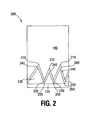
- the lower surface of the layer of piezoelectric material 140 may be rough and may include peaks 210 and valleys 220, as shown in Figure 2 , an enlarged view of the region 200 of Figure 1A . Therefore, the conductive coating 145 formed on the peaks 210 and valleys 220 of the lower surface of the layer of piezoelectric material 140 has a rough surface with peaks 240 and valleys 250. Therefore, when the adhesive 130 is applied to the upper surface of ground layer 125 and/or to conductive coating 145 and is squeezed between ground layer 125 and conductive coating 145 some of valleys 250 of conductive coating 145 may contact ground layer 125, as shown in Figure 2 , thereby electrically coupling conductive coating 145 to ground layer 125.
- a conductive layer 155 is formed overlying and in contact with an upper surface of the layer of piezoelectric material 140, an upper surface fillet 150, and a portion of ground layer 125, as shown in Figure 1A .
- conductive layer 155 may be a metal layer, having at least one of a gold layer, a chromium layer, and a nickel layer.
- conductive layer 155 includes a chromium layer formed overlying and in contact with the upper surface of the layer of piezoelectric material 140, a nickel layer overlying and in contact with the chromium layer, and a gold layer overlying and in contact with the nickel layer.
- the layer of piezoelectric material 140 and conductive layer 155 are divided into portions (e.g., segments) in Figure 1B . Dividing the layer of piezoelectric material 140 into segments forms piezoelectric actuators 160, to 160 N , from piezoelectric material 140, respectively directly overlying channels 120 1 to 120 N . For example, actuators 160 1 to 160 N are directly aligned with channels 120 1 to 120 N on a one-to-one basis.
- Segmenting conductive layer 155 forms upper conductors 162 1 to 162 N , from conductive layer 155, respectively of actuators 160 1 to 160 N , where conductors 162 1 to 162 N respectively overlie and are in contact with the upper surfaces of actuators 160 1 to 160 N . That is, conductors 162 1 to 162 N correspond to actuators 160 1 to 160 N on a one-to-one basis.
- the layer of piezoelectric material 140 and conductive layer 155 are divided into segments mechanically using a mechanical cutting tool, such as a saw or the like, to form slots 165, e.g., cuts, to separate the segments of the layer of piezoelectric material 140, corresponding to actuators 160, from each other and to separate the segments of conductive layer 155, corresponding to conductors 162, from each other.
- a mechanical cutting tool such as a saw or the like
- slot 165 1 separates a portion of the layer of piezoelectric material 140 corresponding to actuator 160 1 from a portion 168 of the layer of piezoelectric material 140 corresponding to a portion of an electrode, such as ground electrode 170, as shown in Figure 1B .
- ground electrode 170 includes the portion 168 of the layer of piezoelectric material 140 and an upper conductor 172 (a portion of conductive layer 155) in contact with the upper surface of the portion 168 and electrically coupled to ground layer 125.
- a ground contact (not shown) may be electrically coupled to ground electrode 170 for coupling ground layer 125 to ground.
- each of slots 165 terminates within the layer of piezoelectric material 140, as shown in Figure 1B , e.g., to prevent the saw from cutting into or through, and thereby destroying, ground layer 125.
- slots 310 e.g., cuts, are formed at either end 350 of each of slots 165 substantially perpendicularly to slots 165 using the saw or the like, as shown in Figure 3A , a top view of a portion of print-head 100 at the stage of fabrication shown in Figure 1B .
- slots 310 are formed to substantially the same depth as slots 165.
- each of slots 310 terminates within the layer of piezoelectric material 140. Note that the stippled portions within slots 165 and 310 in Figure 3A represent piezoelectric material 140 at the bottom of each of slots 165 and 310.
- slots 165 are extended in Figure 1C to expose portions of the upper surface of ground layer 125. This is accomplished by removing, using a beam of electromagnetic radiation, at least a portion of the piezoelectric material 140 at the bottom of each of slots 165 that is connected between neighboring actuators 160, the portion of conductive coating 145 underlying the piezoelectric material 140 at the bottom of each of slots 165, the portion of adhesive 130 underlying the portion of conductive coating 145, and the portion of the ground layer 125 underlying the portion of adhesive 130 to expose a portion of the upper surface of glass layer 115, as indicated by the absence of the stippled portions within slots 165 in Figure 3B , a top view of a portion of print-head 100 at the stage of fabrication shown in Figure 1C .
- the removal process forms lower conductors 180 1 to 180 N , from conductive coating 145, respectively of actuators 160 1 to 160 N , where conductors 180 1 to 180 N respectively underlie and are in contact with the lower surfaces of actuators 160 1 to 160 N , as shown in Figure 1C . That is, conductors 180 1 to 180 N correspond to actuators 160 1 to 160 N on a one-to-one basis. Note that each actuator 160 is sandwiched between an upper conductor 162 and a lower conductor 180, as shown in Figure 1C .
- the removal process also forms a lower conductor 182, from conductive coating 145, of ground electrode 170:
- the piezoelectric material 140 at the bottom of each of slots 310, the portion of conductive coating 145 underlying the piezoelectric material 140 at the bottom of each of slots 310, and the portion of adhesive 130 underlying that portion of conductive coating 145 is not removed, as indicated by the presence of the stippled portions within slots 310 in Figure 3A . Leaving the piezoelectric material 140 at the bottom of each of slots 310, the portion of conductive coating 145 underlying the piezoelectric material 140 at the bottom of each of slots 310, and the portion of adhesive 130 underlying that portion of conductive coating 145 leaves the lower conductor 180 of each actuator 160 electrically coupled to the lower conductors 180 of remaining actuators 160 adjacent either end 350 of each of slots 160.
- contact between the valleys 250 of the one or more of conductors 180 and ground layer 125 electrically couples the conductor 180 of each actuator 160 to ground layer 125 in that conductors 180 of the respective actuators 160 are coupled to each other.
- contact between the valleys 250 of the lower conductor 182 of ground electrode 170 electrically couple conductor 182 to ground layer 125 so that lower conductor 182 and upper conductor 172 are electrically shorted. This means that all of the lower conductors 180 of actuators 160 can be coupled to ground simultaneously by coupling ground electrode 170 to ground.
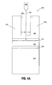
- Figures 4A-4D illustrate region 400 of Figure 1B at different stages of extending slot 165 2 to expose a portion of the upper surface of glass layer 115.
- a beam of electromagnetic radiation 410 such as a laser beam
- a radiation source 420 such as a laser, e.g., a pulsed-laser
- the wavelength of electromagnetic radiation 410 is such that electromagnetic radiation 410 is transmitted through the piezoelectric material 140 at the bottom of slot 165 2 that is connected between neighboring piezoelectric actuators 160 1 and 160 2 .
- the wavelength of electromagnetic radiation 410 is about 500 to about 5000 nanometers.
- the wavelength of electromagnetic radiation 410 is about 1064 nanometers.
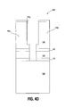
- electromagnetic radiation 410 is transmitted through piezoelectric material 140, electromagnetic radiation 410 is absorbed by conductive coating 145, as shown in Figure 4A .
- the absorbed electromagnetic radiation 410 ablates, e.g., vaporizes, the material of conductive coating 145, as shown in Figure 4B .
- Electromagnetic radiation 410 is subsequently absorbed by adhesive 130.
- the absorbed electromagnetic radiation 410 ablates, e.g., vaporizes, adhesive 130.
- Ablation of adhesive 130 generates forces that act to remove the piezoelectric material 140 at the bottom of slot 165 2 .
- the forces act to breakup and dislodge the piezoelectric material 140.
- ablation of the material of conductive coating 145 and adhesive 130 may occur substantially concurrently, and forces generated by the substantially concurrent ablation of the material of conductive coating 145 and adhesive 130 act to remove the piezoelectric material 140 at the bottom of slot 165 2 .
- Electromagnetic radiation 410 may be subsequently absorbed by ground layer 125, as shown in Figure 4C .
- the absorbed electromagnetic radiation 410 ablates, e.g., vaporizes, the material of ground layer 125, as shown in Figure 4D .
- ablation of adhesive 130 and ground layer 125 may occur substantially concurrently, and forces generated by the substantially concurrent ablation of the material of adhesive 130 and ground layer 125 act to remove the piezoelectric material 140 at the bottom of slot 165 2 .
- ablation of the material of conductive coating 145, adhesive 130, and ground layer 125 may occur substantially concurrently, and forces generated by the substantially concurrent ablation of the material of conductive coating 145, adhesive 130, and ground layer 125 act to remove the piezoelectric material 140 at the bottom of slot 165 2 .
- any remaining loose piezoelectric material 140 may be subsequently removed in a cleaning step, e.g., by a mechanical scrubber, spin-rinse dryer, etc. so that there is no piezoelectric material 140 mechanically and electrically coupling neighboring actuators 160 1 and 160 2 across slot 165 2 , as shown in Figure 4D .
- a cleaning step e.g., by a mechanical scrubber, spin-rinse dryer, etc.
- sidewalls of neighboring actuators 160 1 and 160 2 form opposing sidewalls of slot 165 2 and thus for one embodiment neighboring actuators across a slot refers to actuators whose sidewalls form opposing sidewalls of that slot.
- each slot 165 is devoid of piezoelectric material 140 electrically and mechanically coupling neighboring actuators 160 across that slot and, for example, an actuator 160 and ground electrode 170 across slot 165 1 .
- each slot 160 exposes a portion of an upper surface of glass layer 115, e.g., over the length L ( Figure 3A ) of that slot 165 and over at least a portion of the width W ( Figure 4A ) of that slot. That is, there is no material of conductive coating 145, adhesive 130, and ground layer 125 mechanically and/or electrically coupling neighboring actuators 160 across a slot 165, as shown in Figure 4D for neighboring actuators 160 1 and 160 2 and slot 160 2 , or across slot 165 1 between actuator 160 1 and electrode 170.
- each slot 165 is devoid of material of conductive coating 145, adhesive 130, and ground layer 125 mechanically and/or electrically coupling neighboring actuators 160 across that slot and between an electrode 170 and an actuator 160 across slot 165 1 .
- the beam of electromagnetic radiation 410 scans at least a portion of the width W and the length L of each slot 165. Scanning each slot 165 effects the above removal process of ablating the material of conductive coating 145, adhesive 130, and ground layer 125 using electromagnetic radiation 410 and removal of the piezoelectric material 140 by the forces generated by the ablation of adhesive 130 or by the ablation of adhesive 130 and the material of conductive coating 145, by the ablation of adhesive 130 and the material of ground layer 125, or by the ablation of adhesive 130, the material of conductive coating 145, and the material of ground layer 125.
- glass layer 115 forms a deflectable-layer, such as a pump-layer, of the print-head 100 of Figure 1C , that can be locally deflected (e.g., flexed) in response to applying electric fields to actuators 160.
- an electric field may be selectively applied to an actuator 160, e.g., actuator 160 1 , by selectively applying a voltage to the upper conductor 162, e.g., upper conductor 162 1 , of that actuator 160 while grounding the lower conductor, e.g., lower conductor 180 1 , via ground plane 125 and ground electrode 170.
- the applied electric field causes actuator 160 1 to expand and to exert a local force on a portion 190, denoted by dashed lines in Figure 1C , of glass layer 115 directly aligned with and overlying channel 120 1 .
- the local force acts to flex portion 190 of glass layer 115.
- Flexing portion 190 causes fluid, such as ink, e.g., in the form of a drop, to be ejected from channel 120 1 .
- fluid may be selectively ejected from each channel 120 by selectively applying an electric field to the actuator 160 directly aligned with and overlying that channel 120.
- An advantage of removing the piezoelectric material 140 from slots 165 so that there is no piezoelectric material 140 electrically and mechanically coupling neighboring actuators 160 on either side of the slots 165, as shown in Figure 1C , and between an electrode 170 and an actuator 160, as shown in Figure 1C , is the reduction of cross-talk between the actuators 160, compared to when piezoelectric material 140 left at the bottom of slots 165 electrically and mechanically couples neighboring actuators 160 on either side of the slots 165, as shown in Figure IB.
- Cross-talk can adversely affect print quality, and, therefore, reducing cross-talk by removing the piezoelectric material 140 from slots 165 acts improve print quality compared to when piezoelectric material 140 is left at the bottom of slots 165.
- the mechanical coupling of neighboring actuators 160 across each slot 165 by the material of conductive coating 145, adhesive 130, and ground layer 125 and piezoelectric material 140 acts to reinforce and thereby decreases the compliance of glass layer 115.
- the increased compliance of glass layer 115 effected by removing piezoelectric material 140, the material of conductive coating 145, and adhesive 130 from slots 165, acts to decrease the strength of the electric field that needs to be applied to actuators 160 in order to produce certain drop velocities from the corresponding channels 120. Decreasing the strength of the electric field applied to actuators 160 acts to decrease electric-field induced degradation of the piezoelectric material 140 of actuators 140.
- Embodiments of the method of forming piezoelectric actuators further comprise absorbing the electromagnetic radiation in the conductive layer, wherein absorbing the electromagnetic radiation in the conductive layer ablates the conductive layer.
- Embodiments of the method of forming a fluid-ejection device further comprise forming an other conductive layer overlying the layer of piezoelectric material before forming the at least one slot.
- the electromagnetic radiation has a wavelength of about 500 to about 5000 nanometers.
- the pump-layer is a dielectric layer or a glass layer.
- a conductive layer is interposed between the pump-layer and the plurality of piezoelectric actuators.
- each of the piezoelectric actuators is electrically coupled to the conductive layer.
- the other slot exposes another portion of an upper surface of the pump-layer.
Landscapes
- Engineering & Computer Science (AREA)
- Physics & Mathematics (AREA)
- Optics & Photonics (AREA)
- Manufacturing & Machinery (AREA)
- Plasma & Fusion (AREA)
- Mechanical Engineering (AREA)
- Particle Formation And Scattering Control In Inkjet Printers (AREA)
Claims (14)
- Verfahren zum Bilden piezoelektrischer Stellglieder (1601 bis 160N) auf einer Materialschicht, wobei das Verfahren dadurch gekennzeichnet ist, dass es folgende Schritte umfasst:Entfernen eines piezoelektrischen Materials (140) von der Materialschicht (115), umfassend:Übertragen einer elektromagnetischen Strahlung (410) durch das piezoelektrische Material; undAbsorbieren der elektromagnetischen Strahlung in mindestens einem Klebstoff (130), der das piezoelektrische Material mit der Materialschicht verbindet;wobei das Absorbieren der elektromagnetischen Strahlung in dem mindestens einen Klebstoff den Klebstoff abträgt und das Abtragen des Klebstoffs bewirkt, dass das piezoelektrische Material entfernt wird.
- Das Verfahren nach Anspruch 1, ferner umfassend das Absorbieren der elektromagnetischen Strahlung in einer leitfähigen Schicht (125), die zwischen dem Klebstoff (130) und der Materialschicht (115) eingefügt ist, wobei das Absorbieren der elektromagnetischen Strahlung (415) in der leitfähigen Schicht die leitfähige Schicht abträgt.
- Das Verfahren nach Anspruch 2, ferner umfassend das Absorbieren der elektromagnetischen Strahlung (415) in einer leitfähigen Beschichtung (145), die auf das piezoelektrische Material (140) aufgetragen ist und zwischen dem piezoelektrischen Material und dem Klebstoff (130) eingefügt ist, wobei das Absorbieren der elektromagnetischen Strahlung in der leitfähigen Beschichtung die leitfähige Beschichtung abträgt.
- Das Verfahren nach Anspruch 1, umfassend:Bilden einer leitfähigen Schicht (125), die über der Materialschicht (115) liegt;Verbinden der Schicht aus piezoelektrischem Material (140) mit der leitfähigen Schicht unter Verwendung des Klebstoffs (130);Verwenden eines mechanischen Schneidwerkzeugs, um mindestens einen Schlitz (165) in der Schicht aus piezoelektrischem Material zu bilden, wobei der mindestens eine Schlitz erste und zweite Abschnitte der Schicht aus piezoelektrischem Material auf beiden Seiten des mindestens eine Schlitzes bildet, die jeweils ersten und zweiten piezoelektrischen Stellgliedern (1601, 1602) entsprechen, wobei der mindestens eine Schlitz innerhalb der Schicht aus piezoelektrischem Material endet, so dass sich ein dritter Abschnitt der Schicht aus piezoelektrischem Material innerhalb des mindestens einen Schlitzes zwischen den ersten und zweiten piezoelektrischen Stellgliedern erstreckt;Richten der elektromagnetischen Strahlung (410) in den mindestens einen Schlitz;Übertragen der elektromagnetischen Strahlung durch den dritten Abschnitt der Schicht aus piezoelektrischem Material; undAbsorbieren der elektromagnetischen Strahlung in mindestens dem Klebstoff, der die Schicht aus piezoelektrischem Material mit der Materialschicht verbindet;wobei das Absorbieren der elektromagnetischen Strahlung mindestens in dem Klebstoff den Klebstoff abträgt und das Abtragen des Klebstoffs bewirkt, dass mindestens ein Abschnitt des dritten Abschnitts der Schicht aus piezoelektrischem Material von dem mindestens einen Schlitz entfernt wird.
- Das Verfahren nach Anspruch 4, ferner umfassend das Absorbieren der elektromagnetischen Strahlung (410) in der leitfähigen Schicht (125), wobei das Absorbieren der elektromagnetischen Strahlung in der leitfähigen Schicht die leitfähige Schicht (125) abträgt, und wobei das Abtragen des Klebstoffs (130) und der leitfähigen Schicht im Wesentlichen gleichzeitig erfolgt, und wobei das im Wesentlichen gleichzeitige Abtragen des Klebstoffs und der leitfähigen Schicht bewirkt, dass der mindestens eine Abschnitt des dritten Abschnitts der Schicht aus piezoelektrischem Material (140) aus dem mindestens einen Schlitz (165) entfernt wird.
- Das Verfahren nach Anspruch 1, wobei jeder der piezoelektrischen Stellglieder elektrisch mit der leitfähigen Schicht gekoppelt ist.
- Das Verfahren nach Anspruch 1, wobei die Wellenlänge der elektromagnetischen Strahlung (410) ungefähr 500 bis ungefähr 5000 Nanometer beträgt.
- Das Verfahren nach Anspruch 1, wobei der Klebstoff (130) ein elektrischer Isolator ist.
- Das Verfahren nach Anspruch 1, wobei der Klebstoff (130) ein Epoxidharz ist.
- Das Verfahren des Bildens einer Fluidausstoßvorrichtung (100), umfassend:Bilden einer Pumpschicht (115), die über einem Substrat (110) liegt, wobei in dem Substrat mindestens ein Fluidabgabekanal (120) gebildet ist;Bilden einer leitfähigen Schicht (125), die über der Pumpschicht liegt;Verbinden einer Schicht aus piezoelektrischem Material (140) mit der leitfähigen Schicht;Verwenden eines mechanischen Schneidwerkzeugs, um mindestens einen Schlitz (165) in der Schicht aus piezoelektrischem Material zu bilden, wobei der mindestens eine Schlitz erste und zweite Abschnitte der Schicht aus piezoelektrischem Material auf beiden Seiten des mindestens einen Schlitzes bildet, wobei der mindestens eine Schlitz innerhalb der Schicht aus piezoelektrischem Material endet, so dass sich ein dritter Abschnitt der Schicht aus piezoelektrischem Material innerhalb des mindestens einen Schlitzes zwischen den ersten und zweiten Abschnitten der Schicht aus piezoelektrischem Material erstreckt, wobei mindestens einer der ersten und zweiten Abschnitte der Schicht aus piezoelektrischem Material ein piezoelektrisches Stellglied (160) bildet, das direkt mit dem mindestens einen Fluidabgabekanal fluchtet;Entfernen mindestens eines Abschnitts des dritten Abschnitts der Schicht aus piezoelektrischem Material aus dem mindestens einen Schlitz unter Verwendung eines Verfahrens nach einem der Ansprüche 1 bis 3,wobei elektromagnetische Strahlung (410) in den mindestens einen Schlitz gerichtet ist;wobei die elektromagnetische Strahlung durch den dritten Abschnitt der Schicht aus piezoelektrischem Material übertragen wird; undwobei die elektromagnetische Strahlung in mindestens einem Klebstoff (130) absorbiert wird, der die Schicht aus piezoelektrischem Material mit der leitfähigen Schicht verbindet.
- Das Verfahren nach Anspruch 10, ferner umfassend:Absorbieren der elektromagnetischen Strahlung (410) in einer leitfähigen Beschichtung (145), die auf einer unteren Oberfläche der Schicht aus piezoelektrischem Material gebildet ist, wobei das Absorbieren der elektromagnetischen Strahlung in der leitfähigen Beschichtung die leitfähige Beschichtung abträgt; undAbsorbieren der elektromagnetischen Strahlung in der leitfähigen Schicht (125), wobei das Absorbieren der elektromagnetischen Strahlung in der leitfähigen Schicht die leitfähige Schicht abträgt.
- Das Verfahren nach Anspruch 11, wobei das Abtragen des Klebstoffs (130), der leitfähigen Beschichtung (145) und der leitfähigen Schicht (125) im Wesentlichen gleichzeitig erfolgt, und wobei das im Wesentlichen gleichzeitige Abtragen des Klebstoffs, der leitfähigen Beschichtung und der leitfähigen Schicht bewirkt, dass der mindestens eine Abschnitt des dritten Abschnitts der Schicht aus piezoelektrischem Material (140) aus dem mindestens einen Schlitz (165) entfernt wird.
- Das Verfahren nach Anspruch 11, wobei das Abtragen des Klebstoffs (130), der leitfähigen Beschichtung (145) und der leitfähigen Schicht (125) und das Entfernen des mindestens einen Abschnitts des dritten Abschnitts der Schicht aus piezoelektrischem Material (140) aus dem mindestens einen Schlitz eine obere Oberfläche der Pumpschicht (115) freilegt.
- Das Verfahren nach Anspruch 10, ferner umfassend das Bilden einer andern leitfähigen Schicht (172), die auf der Schicht aus piezoelektrischem Material liegt, bevor der mindestens eine Schlitz gebildet wird,
ferner umfassend das Bilden des mindestens einen Schlitzes (165) durch die andere leitfähige Schicht, um erste und zweite Abschnitte der anderen leitfähigen Schicht zu bilden, die jeweils über den ersten und zweiten Abschnitten der Schicht aus piezoelektrischem Material (140) liegen.
Applications Claiming Priority (1)
| Application Number | Priority Date | Filing Date | Title |
|---|---|---|---|
| PCT/US2008/077308 WO2010036235A1 (en) | 2008-09-23 | 2008-09-23 | Removing piezoelectric material using electromagnetic radiation |
Publications (3)
| Publication Number | Publication Date |
|---|---|
| EP2327115A1 EP2327115A1 (de) | 2011-06-01 |
| EP2327115A4 EP2327115A4 (de) | 2012-09-12 |
| EP2327115B1 true EP2327115B1 (de) | 2013-11-06 |
Family
ID=42059981
Family Applications (1)
| Application Number | Title | Priority Date | Filing Date |
|---|---|---|---|
| EP20080823247 Not-in-force EP2327115B1 (de) | 2008-09-23 | 2008-09-23 | Entfernung von piezoelektrischem material unter verwendung elektromagnetischer strahlung |
Country Status (5)
| Country | Link |
|---|---|
| US (1) | US9021699B2 (de) |
| EP (1) | EP2327115B1 (de) |
| JP (1) | JP5409791B2 (de) |
| CN (1) | CN102165617B (de) |
| WO (1) | WO2010036235A1 (de) |
Families Citing this family (2)
| Publication number | Priority date | Publication date | Assignee | Title |
|---|---|---|---|---|
| US20140097003A1 (en) * | 2012-10-05 | 2014-04-10 | Tyco Electronics Amp Gmbh | Electrical components and methods and systems of manufacturing electrical components |
| EP3127616B1 (de) * | 2015-08-03 | 2017-10-18 | PARI Pharma GmbH | Verfahren zur herstellung eines schwingungsfähigen kopfs für einen aerosolgenerator und schwingungsfähiger kopf für einen aerosolgenerator |
Family Cites Families (19)
| Publication number | Priority date | Publication date | Assignee | Title |
|---|---|---|---|---|
| US4328410A (en) * | 1978-08-24 | 1982-05-04 | Slivinsky Sandra H | Laser skiving system |
| DE3804165A1 (de) * | 1988-02-11 | 1989-08-24 | Olympia Aeg | Verfahren zum bestuecken eines tintenstrahldruckkopfes mit piezokristallen |
| JPH0373348A (ja) | 1989-05-12 | 1991-03-28 | Ricoh Co Ltd | インクジェット記録装置 |
| GB9318985D0 (en) * | 1993-09-14 | 1993-10-27 | Xaar Ltd | Passivation of ceramic piezoelectric ink jet print heads |
| US5505364A (en) * | 1993-12-30 | 1996-04-09 | Compaq Computer Corporation | Method of manufacturing ink jet printheads |
| US5535494A (en) * | 1994-09-23 | 1996-07-16 | Compaq Computer Corporation | Method of fabricating a piezoelectric ink jet printhead assembly |
| US5534594A (en) * | 1994-12-05 | 1996-07-09 | Rohm And Haas Company | Preparation of butadiene-based impact modifiers |
| US6188416B1 (en) * | 1997-02-13 | 2001-02-13 | Microfab Technologies, Inc. | Orifice array for high density ink jet printhead |
| JP2873287B1 (ja) * | 1998-03-20 | 1999-03-24 | 新潟日本電気株式会社 | インクジェット記録ヘッドおよびその製造方法 |
| US6291088B1 (en) * | 1998-09-30 | 2001-09-18 | Xerox Corporation | Inorganic overcoat for particulate transport electrode grid |
| US6511149B1 (en) * | 1998-09-30 | 2003-01-28 | Xerox Corporation | Ballistic aerosol marking apparatus for marking a substrate |
| JP4736174B2 (ja) | 2000-11-14 | 2011-07-27 | コニカミノルタホールディングス株式会社 | インクジェットヘッドのノズル穴形成方法 |
| JP2006344618A (ja) | 2005-06-07 | 2006-12-21 | Fujifilm Holdings Corp | 機能性膜含有構造体、及び、機能性膜の製造方法 |
| US20070046153A1 (en) * | 2005-08-23 | 2007-03-01 | Canon Kabushiki Kaisha | Piezoelectric substrate, piezoelectric element, liquid discharge head and liquid discharge apparatus |
| US7862678B2 (en) | 2006-04-05 | 2011-01-04 | Xerox Corporation | Drop generator |
| JP2007296777A (ja) | 2006-05-01 | 2007-11-15 | Canon Inc | インクジェット記録ヘッドおよびインクジェット記録ヘッドの製造方法 |
| JP2008049569A (ja) | 2006-08-24 | 2008-03-06 | Brother Ind Ltd | 液体移送装置及び液体移送装置の製造方法 |
| EP1958777B1 (de) | 2007-02-16 | 2013-08-14 | Brother Kogyo Kabushiki Kaisha | Herstellungsverfahren für einen piezoelektrischen Auslöser und Herstellungsverfahren für ein Transportgerät |
| JP2008198959A (ja) | 2007-02-16 | 2008-08-28 | Brother Ind Ltd | 圧電アクチュエータの製造方法、及び、液体移送装置の製造方法 |
-
2008
- 2008-09-23 EP EP20080823247 patent/EP2327115B1/de not_active Not-in-force
- 2008-09-23 WO PCT/US2008/077308 patent/WO2010036235A1/en not_active Ceased
- 2008-09-23 CN CN200880131227.2A patent/CN102165617B/zh not_active Expired - Fee Related
- 2008-09-23 US US13/061,722 patent/US9021699B2/en not_active Expired - Fee Related
- 2008-09-23 JP JP2011527790A patent/JP5409791B2/ja not_active Expired - Fee Related
Also Published As
| Publication number | Publication date |
|---|---|
| JP5409791B2 (ja) | 2014-02-05 |
| JP2012503862A (ja) | 2012-02-09 |
| CN102165617A (zh) | 2011-08-24 |
| EP2327115A4 (de) | 2012-09-12 |
| US20110168807A1 (en) | 2011-07-14 |
| WO2010036235A1 (en) | 2010-04-01 |
| CN102165617B (zh) | 2014-04-09 |
| EP2327115A1 (de) | 2011-06-01 |
| US9021699B2 (en) | 2015-05-05 |
Similar Documents
| Publication | Publication Date | Title |
|---|---|---|
| EP1997635B1 (de) | Piezoelektrischer Aktuator und Herstellungsverfahren dafür | |
| TWI390779B (zh) | 形成壓電致動器的方法 | |
| JP5242238B2 (ja) | 圧電インクジェットデバイスの製作方法 | |
| JP2011037057A (ja) | インクジェットヘッドの製造方法 | |
| EP1815537B1 (de) | Verfahren zur bildung einer einrichtung mit einem piezoelektrischen wandler | |
| JP5502020B2 (ja) | インクジェットヘッド及びインクジェットヘッドの製造方法 | |
| EP1997638B1 (de) | Verfahren zur Erzeugung eines Arrays piezoelektrischer Aktuatoren auf einer Membran | |
| EP2327115B1 (de) | Entfernung von piezoelektrischem material unter verwendung elektromagnetischer strahlung | |
| US8784591B2 (en) | Process for producing liquid ejection head | |
| JP2010179622A (ja) | 液体噴射ヘッド、液体噴射装置、および液体噴射ヘッドの製造方法 | |
| JPH11334088A (ja) | インクジェット記録ヘッドの製造方法 | |
| KR20030034214A (ko) | 액적 증착 장치 | |
| KR101700100B1 (ko) | 접합 마이크로전자기계 조립체 | |
| US6722035B1 (en) | Method of manufacturing an ink ejecting device wherein electrodes formed within non-ejecting channels are divided and electrodes formed within ejecting channels are continuous | |
| JP6140941B2 (ja) | 液体吐出ヘッドとその製造方法 | |
| JP6006992B2 (ja) | マルチノズルプレートの製造方法 | |
| JP3850298B2 (ja) | インクジェットヘッドおよびその製造方法 | |
| JP2002120367A (ja) | インクジェットヘッドとその製造方法 | |
| JP3706034B2 (ja) | インクジェットヘッドの製造方法 | |
| JP2006181828A (ja) | 液体噴射ヘッドの製造方法及び液体噴射ヘッド | |
| JP2006256232A (ja) | 液滴吐出ヘッドおよびその製造方法並びに記録装置、積層基板の分割方法及び、積層体 |
Legal Events
| Date | Code | Title | Description |
|---|---|---|---|
| PUAI | Public reference made under article 153(3) epc to a published international application that has entered the european phase |
Free format text: ORIGINAL CODE: 0009012 |
|
| 17P | Request for examination filed |
Effective date: 20110225 |
|
| AK | Designated contracting states |
Kind code of ref document: A1 Designated state(s): AT BE BG CH CY CZ DE DK EE ES FI FR GB GR HR HU IE IS IT LI LT LU LV MC MT NL NO PL PT RO SE SI SK TR |
|
| AX | Request for extension of the european patent |
Extension state: AL BA MK RS |
|
| DAX | Request for extension of the european patent (deleted) | ||
| A4 | Supplementary search report drawn up and despatched |
Effective date: 20120813 |
|
| RIC1 | Information provided on ipc code assigned before grant |
Ipc: H01L 41/04 20060101ALI20120807BHEP Ipc: B41J 2/16 20060101ALI20120807BHEP Ipc: B23K 26/38 20060101ALI20120807BHEP Ipc: B23K 26/36 20060101ALI20120807BHEP Ipc: H01L 21/302 20060101ALI20120807BHEP Ipc: B23K 26/40 20060101ALI20120807BHEP Ipc: H01L 41/08 20060101AFI20120807BHEP |
|
| REG | Reference to a national code |
Ref country code: DE Ref legal event code: R079 Ref document number: 602008028619 Country of ref document: DE Free format text: PREVIOUS MAIN CLASS: H01L0041080000 Ipc: H01L0041313000 |
|
| RIC1 | Information provided on ipc code assigned before grant |
Ipc: H01L 21/302 20060101ALI20130402BHEP Ipc: H01L 41/04 20060101ALI20130402BHEP Ipc: B41J 2/16 20060101ALI20130402BHEP Ipc: H01L 41/08 20060101AFI20130402BHEP Ipc: B23K 26/38 20060101ALI20130402BHEP Ipc: B23K 26/36 20060101ALI20130402BHEP Ipc: B23K 26/40 20060101ALI20130402BHEP |
|
| RIC1 | Information provided on ipc code assigned before grant |
Ipc: B41J 2/16 20060101ALI20130424BHEP Ipc: H01L 41/338 20130101ALI20130424BHEP Ipc: H01L 41/313 20130101AFI20130424BHEP Ipc: B23K 26/36 20060101ALI20130424BHEP Ipc: B23K 26/38 20060101ALI20130424BHEP Ipc: H01L 21/302 20060101ALI20130424BHEP Ipc: B23K 26/40 20060101ALI20130424BHEP |
|
| GRAP | Despatch of communication of intention to grant a patent |
Free format text: ORIGINAL CODE: EPIDOSNIGR1 |
|
| INTG | Intention to grant announced |
Effective date: 20130808 |
|
| RAP1 | Party data changed (applicant data changed or rights of an application transferred) |
Owner name: HEWLETT-PACKARD DEVELOPMENT COMPANY, L.P. |
|
| GRAS | Grant fee paid |
Free format text: ORIGINAL CODE: EPIDOSNIGR3 |
|
| GRAA | (expected) grant |
Free format text: ORIGINAL CODE: 0009210 |
|
| AK | Designated contracting states |
Kind code of ref document: B1 Designated state(s): AT BE BG CH CY CZ DE DK EE ES FI FR GB GR HR HU IE IS IT LI LT LU LV MC MT NL NO PL PT RO SE SI SK TR |
|
| REG | Reference to a national code |
Ref country code: GB Ref legal event code: FG4D |
|
| REG | Reference to a national code |
Ref country code: CH Ref legal event code: EP |
|
| REG | Reference to a national code |
Ref country code: AT Ref legal event code: REF Ref document number: 639966 Country of ref document: AT Kind code of ref document: T Effective date: 20131215 |
|
| REG | Reference to a national code |
Ref country code: IE Ref legal event code: FG4D |
|
| REG | Reference to a national code |
Ref country code: DE Ref legal event code: R096 Ref document number: 602008028619 Country of ref document: DE Effective date: 20140102 |
|
| REG | Reference to a national code |
Ref country code: NL Ref legal event code: VDEP Effective date: 20131106 |
|
| REG | Reference to a national code |
Ref country code: AT Ref legal event code: MK05 Ref document number: 639966 Country of ref document: AT Kind code of ref document: T Effective date: 20131106 |
|
| REG | Reference to a national code |
Ref country code: LT Ref legal event code: MG4D |
|
| PG25 | Lapsed in a contracting state [announced via postgrant information from national office to epo] |
Ref country code: FI Free format text: LAPSE BECAUSE OF FAILURE TO SUBMIT A TRANSLATION OF THE DESCRIPTION OR TO PAY THE FEE WITHIN THE PRESCRIBED TIME-LIMIT Effective date: 20131106 Ref country code: SE Free format text: LAPSE BECAUSE OF FAILURE TO SUBMIT A TRANSLATION OF THE DESCRIPTION OR TO PAY THE FEE WITHIN THE PRESCRIBED TIME-LIMIT Effective date: 20131106 Ref country code: IS Free format text: LAPSE BECAUSE OF FAILURE TO SUBMIT A TRANSLATION OF THE DESCRIPTION OR TO PAY THE FEE WITHIN THE PRESCRIBED TIME-LIMIT Effective date: 20140306 Ref country code: LT Free format text: LAPSE BECAUSE OF FAILURE TO SUBMIT A TRANSLATION OF THE DESCRIPTION OR TO PAY THE FEE WITHIN THE PRESCRIBED TIME-LIMIT Effective date: 20131106 Ref country code: HR Free format text: LAPSE BECAUSE OF FAILURE TO SUBMIT A TRANSLATION OF THE DESCRIPTION OR TO PAY THE FEE WITHIN THE PRESCRIBED TIME-LIMIT Effective date: 20131106 Ref country code: NL Free format text: LAPSE BECAUSE OF FAILURE TO SUBMIT A TRANSLATION OF THE DESCRIPTION OR TO PAY THE FEE WITHIN THE PRESCRIBED TIME-LIMIT Effective date: 20131106 Ref country code: NO Free format text: LAPSE BECAUSE OF FAILURE TO SUBMIT A TRANSLATION OF THE DESCRIPTION OR TO PAY THE FEE WITHIN THE PRESCRIBED TIME-LIMIT Effective date: 20140206 |
|
| PG25 | Lapsed in a contracting state [announced via postgrant information from national office to epo] |
Ref country code: LV Free format text: LAPSE BECAUSE OF FAILURE TO SUBMIT A TRANSLATION OF THE DESCRIPTION OR TO PAY THE FEE WITHIN THE PRESCRIBED TIME-LIMIT Effective date: 20131106 Ref country code: BE Free format text: LAPSE BECAUSE OF FAILURE TO SUBMIT A TRANSLATION OF THE DESCRIPTION OR TO PAY THE FEE WITHIN THE PRESCRIBED TIME-LIMIT Effective date: 20131106 Ref country code: ES Free format text: LAPSE BECAUSE OF FAILURE TO SUBMIT A TRANSLATION OF THE DESCRIPTION OR TO PAY THE FEE WITHIN THE PRESCRIBED TIME-LIMIT Effective date: 20131106 Ref country code: AT Free format text: LAPSE BECAUSE OF FAILURE TO SUBMIT A TRANSLATION OF THE DESCRIPTION OR TO PAY THE FEE WITHIN THE PRESCRIBED TIME-LIMIT Effective date: 20131106 |
|
| PG25 | Lapsed in a contracting state [announced via postgrant information from national office to epo] |
Ref country code: PT Free format text: LAPSE BECAUSE OF FAILURE TO SUBMIT A TRANSLATION OF THE DESCRIPTION OR TO PAY THE FEE WITHIN THE PRESCRIBED TIME-LIMIT Effective date: 20140306 |
|
| PG25 | Lapsed in a contracting state [announced via postgrant information from national office to epo] |
Ref country code: EE Free format text: LAPSE BECAUSE OF FAILURE TO SUBMIT A TRANSLATION OF THE DESCRIPTION OR TO PAY THE FEE WITHIN THE PRESCRIBED TIME-LIMIT Effective date: 20131106 |
|
| REG | Reference to a national code |
Ref country code: DE Ref legal event code: R097 Ref document number: 602008028619 Country of ref document: DE |
|
| PG25 | Lapsed in a contracting state [announced via postgrant information from national office to epo] |
Ref country code: PL Free format text: LAPSE BECAUSE OF FAILURE TO SUBMIT A TRANSLATION OF THE DESCRIPTION OR TO PAY THE FEE WITHIN THE PRESCRIBED TIME-LIMIT Effective date: 20131106 Ref country code: SK Free format text: LAPSE BECAUSE OF FAILURE TO SUBMIT A TRANSLATION OF THE DESCRIPTION OR TO PAY THE FEE WITHIN THE PRESCRIBED TIME-LIMIT Effective date: 20131106 Ref country code: IT Free format text: LAPSE BECAUSE OF FAILURE TO SUBMIT A TRANSLATION OF THE DESCRIPTION OR TO PAY THE FEE WITHIN THE PRESCRIBED TIME-LIMIT Effective date: 20131106 Ref country code: RO Free format text: LAPSE BECAUSE OF FAILURE TO SUBMIT A TRANSLATION OF THE DESCRIPTION OR TO PAY THE FEE WITHIN THE PRESCRIBED TIME-LIMIT Effective date: 20131106 Ref country code: CZ Free format text: LAPSE BECAUSE OF FAILURE TO SUBMIT A TRANSLATION OF THE DESCRIPTION OR TO PAY THE FEE WITHIN THE PRESCRIBED TIME-LIMIT Effective date: 20131106 |
|
| PLBE | No opposition filed within time limit |
Free format text: ORIGINAL CODE: 0009261 |
|
| STAA | Information on the status of an ep patent application or granted ep patent |
Free format text: STATUS: NO OPPOSITION FILED WITHIN TIME LIMIT |
|
| PG25 | Lapsed in a contracting state [announced via postgrant information from national office to epo] |
Ref country code: DK Free format text: LAPSE BECAUSE OF FAILURE TO SUBMIT A TRANSLATION OF THE DESCRIPTION OR TO PAY THE FEE WITHIN THE PRESCRIBED TIME-LIMIT Effective date: 20131106 |
|
| 26N | No opposition filed |
Effective date: 20140807 |
|
| REG | Reference to a national code |
Ref country code: DE Ref legal event code: R097 Ref document number: 602008028619 Country of ref document: DE Effective date: 20140807 |
|
| PG25 | Lapsed in a contracting state [announced via postgrant information from national office to epo] |
Ref country code: SI Free format text: LAPSE BECAUSE OF FAILURE TO SUBMIT A TRANSLATION OF THE DESCRIPTION OR TO PAY THE FEE WITHIN THE PRESCRIBED TIME-LIMIT Effective date: 20131106 |
|
| PG25 | Lapsed in a contracting state [announced via postgrant information from national office to epo] |
Ref country code: MC Free format text: LAPSE BECAUSE OF FAILURE TO SUBMIT A TRANSLATION OF THE DESCRIPTION OR TO PAY THE FEE WITHIN THE PRESCRIBED TIME-LIMIT Effective date: 20131106 Ref country code: LU Free format text: LAPSE BECAUSE OF FAILURE TO SUBMIT A TRANSLATION OF THE DESCRIPTION OR TO PAY THE FEE WITHIN THE PRESCRIBED TIME-LIMIT Effective date: 20140923 |
|
| REG | Reference to a national code |
Ref country code: CH Ref legal event code: PL |
|
| GBPC | Gb: european patent ceased through non-payment of renewal fee |
Effective date: 20140923 |
|
| REG | Reference to a national code |
Ref country code: IE Ref legal event code: MM4A |
|
| REG | Reference to a national code |
Ref country code: FR Ref legal event code: ST Effective date: 20150529 |
|
| PG25 | Lapsed in a contracting state [announced via postgrant information from national office to epo] |
Ref country code: LI Free format text: LAPSE BECAUSE OF NON-PAYMENT OF DUE FEES Effective date: 20140930 Ref country code: CH Free format text: LAPSE BECAUSE OF NON-PAYMENT OF DUE FEES Effective date: 20140930 Ref country code: GB Free format text: LAPSE BECAUSE OF NON-PAYMENT OF DUE FEES Effective date: 20140923 |
|
| PG25 | Lapsed in a contracting state [announced via postgrant information from national office to epo] |
Ref country code: IE Free format text: LAPSE BECAUSE OF NON-PAYMENT OF DUE FEES Effective date: 20140923 Ref country code: FR Free format text: LAPSE BECAUSE OF NON-PAYMENT OF DUE FEES Effective date: 20140930 |
|
| PG25 | Lapsed in a contracting state [announced via postgrant information from national office to epo] |
Ref country code: BG Free format text: LAPSE BECAUSE OF FAILURE TO SUBMIT A TRANSLATION OF THE DESCRIPTION OR TO PAY THE FEE WITHIN THE PRESCRIBED TIME-LIMIT Effective date: 20131106 |
|
| PG25 | Lapsed in a contracting state [announced via postgrant information from national office to epo] |
Ref country code: MT Free format text: LAPSE BECAUSE OF FAILURE TO SUBMIT A TRANSLATION OF THE DESCRIPTION OR TO PAY THE FEE WITHIN THE PRESCRIBED TIME-LIMIT Effective date: 20131106 Ref country code: CY Free format text: LAPSE BECAUSE OF FAILURE TO SUBMIT A TRANSLATION OF THE DESCRIPTION OR TO PAY THE FEE WITHIN THE PRESCRIBED TIME-LIMIT Effective date: 20131106 Ref country code: GR Free format text: LAPSE BECAUSE OF FAILURE TO SUBMIT A TRANSLATION OF THE DESCRIPTION OR TO PAY THE FEE WITHIN THE PRESCRIBED TIME-LIMIT Effective date: 20140207 |
|
| PG25 | Lapsed in a contracting state [announced via postgrant information from national office to epo] |
Ref country code: TR Free format text: LAPSE BECAUSE OF FAILURE TO SUBMIT A TRANSLATION OF THE DESCRIPTION OR TO PAY THE FEE WITHIN THE PRESCRIBED TIME-LIMIT Effective date: 20131106 Ref country code: HU Free format text: LAPSE BECAUSE OF FAILURE TO SUBMIT A TRANSLATION OF THE DESCRIPTION OR TO PAY THE FEE WITHIN THE PRESCRIBED TIME-LIMIT; INVALID AB INITIO Effective date: 20080923 |
|
| PGFP | Annual fee paid to national office [announced via postgrant information from national office to epo] |
Ref country code: DE Payment date: 20170821 Year of fee payment: 10 |
|
| REG | Reference to a national code |
Ref country code: DE Ref legal event code: R119 Ref document number: 602008028619 Country of ref document: DE |
|
| PG25 | Lapsed in a contracting state [announced via postgrant information from national office to epo] |
Ref country code: DE Free format text: LAPSE BECAUSE OF NON-PAYMENT OF DUE FEES Effective date: 20190402 |