EP2325875A1 - Semiconductor device - Google Patents
Semiconductor device Download PDFInfo
- Publication number
- EP2325875A1 EP2325875A1 EP09812805A EP09812805A EP2325875A1 EP 2325875 A1 EP2325875 A1 EP 2325875A1 EP 09812805 A EP09812805 A EP 09812805A EP 09812805 A EP09812805 A EP 09812805A EP 2325875 A1 EP2325875 A1 EP 2325875A1
- Authority
- EP
- European Patent Office
- Prior art keywords
- die bonding
- semiconductor element
- bonding resin
- semiconductor device
- bonding pad
- Prior art date
- Legal status (The legal status is an assumption and is not a legal conclusion. Google has not performed a legal analysis and makes no representation as to the accuracy of the status listed.)
- Granted
Links
Images





Classifications
-
- H—ELECTRICITY
- H10—SEMICONDUCTOR DEVICES; ELECTRIC SOLID-STATE DEVICES NOT OTHERWISE PROVIDED FOR
- H10W—GENERIC PACKAGES, INTERCONNECTIONS, CONNECTORS OR OTHER CONSTRUCTIONAL DETAILS OF DEVICES COVERED BY CLASS H10
- H10W72/00—Interconnections or connectors in packages
-
- H—ELECTRICITY
- H04—ELECTRIC COMMUNICATION TECHNIQUE
- H04R—LOUDSPEAKERS, MICROPHONES, GRAMOPHONE PICK-UPS OR LIKE ACOUSTIC ELECTROMECHANICAL TRANSDUCERS; ELECTRIC HEARING AIDS; PUBLIC ADDRESS SYSTEMS
- H04R31/00—Apparatus or processes specially adapted for the manufacture of transducers or diaphragms therefor
- H04R31/006—Interconnection of transducer parts
-
- B—PERFORMING OPERATIONS; TRANSPORTING
- B81—MICROSTRUCTURAL TECHNOLOGY
- B81C—PROCESSES OR APPARATUS SPECIALLY ADAPTED FOR THE MANUFACTURE OR TREATMENT OF MICROSTRUCTURAL DEVICES OR SYSTEMS
- B81C3/00—Assembling of devices or systems from individually processed components
- B81C3/001—Bonding of two components
-
- H—ELECTRICITY
- H10—SEMICONDUCTOR DEVICES; ELECTRIC SOLID-STATE DEVICES NOT OTHERWISE PROVIDED FOR
- H10W—GENERIC PACKAGES, INTERCONNECTIONS, CONNECTORS OR OTHER CONSTRUCTIONAL DETAILS OF DEVICES COVERED BY CLASS H10
- H10W42/00—Arrangements for protection of devices
- H10W42/20—Arrangements for protection of devices protecting against electromagnetic or particle radiation, e.g. light, X-rays, gamma-rays or electrons
-
- B—PERFORMING OPERATIONS; TRANSPORTING
- B81—MICROSTRUCTURAL TECHNOLOGY
- B81B—MICROSTRUCTURAL DEVICES OR SYSTEMS, e.g. MICROMECHANICAL DEVICES
- B81B2201/00—Specific applications of microelectromechanical systems
- B81B2201/02—Sensors
- B81B2201/0257—Microphones or microspeakers
-
- B—PERFORMING OPERATIONS; TRANSPORTING
- B81—MICROSTRUCTURAL TECHNOLOGY
- B81B—MICROSTRUCTURAL DEVICES OR SYSTEMS, e.g. MICROMECHANICAL DEVICES
- B81B2203/00—Basic microelectromechanical structures
- B81B2203/03—Static structures
- B81B2203/0369—Static structures characterized by their profile
- B81B2203/0392—Static structures characterized by their profile profiles not provided for in B81B2203/0376 - B81B2203/0384
-
- H—ELECTRICITY
- H04—ELECTRIC COMMUNICATION TECHNIQUE
- H04R—LOUDSPEAKERS, MICROPHONES, GRAMOPHONE PICK-UPS OR LIKE ACOUSTIC ELECTROMECHANICAL TRANSDUCERS; ELECTRIC HEARING AIDS; PUBLIC ADDRESS SYSTEMS
- H04R19/00—Electrostatic transducers
- H04R19/005—Electrostatic transducers using semiconductor materials
-
- H—ELECTRICITY
- H04—ELECTRIC COMMUNICATION TECHNIQUE
- H04R—LOUDSPEAKERS, MICROPHONES, GRAMOPHONE PICK-UPS OR LIKE ACOUSTIC ELECTROMECHANICAL TRANSDUCERS; ELECTRIC HEARING AIDS; PUBLIC ADDRESS SYSTEMS
- H04R19/00—Electrostatic transducers
- H04R19/04—Microphones
-
- H—ELECTRICITY
- H10—SEMICONDUCTOR DEVICES; ELECTRIC SOLID-STATE DEVICES NOT OTHERWISE PROVIDED FOR
- H10W—GENERIC PACKAGES, INTERCONNECTIONS, CONNECTORS OR OTHER CONSTRUCTIONAL DETAILS OF DEVICES COVERED BY CLASS H10
- H10W72/00—Interconnections or connectors in packages
- H10W72/01—Manufacture or treatment
- H10W72/013—Manufacture or treatment of die-attach connectors
- H10W72/01321—Manufacture or treatment of die-attach connectors using local deposition
- H10W72/01323—Manufacture or treatment of die-attach connectors using local deposition in liquid form, e.g. by dispensing droplets or by screen printing
-
- H—ELECTRICITY
- H10—SEMICONDUCTOR DEVICES; ELECTRIC SOLID-STATE DEVICES NOT OTHERWISE PROVIDED FOR
- H10W—GENERIC PACKAGES, INTERCONNECTIONS, CONNECTORS OR OTHER CONSTRUCTIONAL DETAILS OF DEVICES COVERED BY CLASS H10
- H10W72/00—Interconnections or connectors in packages
- H10W72/071—Connecting or disconnecting
- H10W72/073—Connecting or disconnecting of die-attach connectors
-
- H—ELECTRICITY
- H10—SEMICONDUCTOR DEVICES; ELECTRIC SOLID-STATE DEVICES NOT OTHERWISE PROVIDED FOR
- H10W—GENERIC PACKAGES, INTERCONNECTIONS, CONNECTORS OR OTHER CONSTRUCTIONAL DETAILS OF DEVICES COVERED BY CLASS H10
- H10W72/00—Interconnections or connectors in packages
- H10W72/071—Connecting or disconnecting
- H10W72/073—Connecting or disconnecting of die-attach connectors
- H10W72/07331—Connecting techniques
- H10W72/07337—Connecting techniques using a polymer adhesive, e.g. an adhesive based on silicone or epoxy
- H10W72/07338—Connecting techniques using a polymer adhesive, e.g. an adhesive based on silicone or epoxy hardening the adhesive by curing, e.g. thermosetting
-
- H—ELECTRICITY
- H10—SEMICONDUCTOR DEVICES; ELECTRIC SOLID-STATE DEVICES NOT OTHERWISE PROVIDED FOR
- H10W—GENERIC PACKAGES, INTERCONNECTIONS, CONNECTORS OR OTHER CONSTRUCTIONAL DETAILS OF DEVICES COVERED BY CLASS H10
- H10W72/00—Interconnections or connectors in packages
- H10W72/30—Die-attach connectors
- H10W72/351—Materials of die-attach connectors
- H10W72/353—Materials of die-attach connectors not comprising solid metals or solid metalloids, e.g. ceramics
- H10W72/354—Materials of die-attach connectors not comprising solid metals or solid metalloids, e.g. ceramics comprising polymers
-
- H—ELECTRICITY
- H10—SEMICONDUCTOR DEVICES; ELECTRIC SOLID-STATE DEVICES NOT OTHERWISE PROVIDED FOR
- H10W—GENERIC PACKAGES, INTERCONNECTIONS, CONNECTORS OR OTHER CONSTRUCTIONAL DETAILS OF DEVICES COVERED BY CLASS H10
- H10W72/00—Interconnections or connectors in packages
- H10W72/851—Dispositions of multiple connectors or interconnections
- H10W72/874—On different surfaces
- H10W72/884—Die-attach connectors and bond wires
-
- H—ELECTRICITY
- H10—SEMICONDUCTOR DEVICES; ELECTRIC SOLID-STATE DEVICES NOT OTHERWISE PROVIDED FOR
- H10W—GENERIC PACKAGES, INTERCONNECTIONS, CONNECTORS OR OTHER CONSTRUCTIONAL DETAILS OF DEVICES COVERED BY CLASS H10
- H10W72/00—Interconnections or connectors in packages
- H10W72/90—Bond pads, in general
- H10W72/951—Materials of bond pads
- H10W72/952—Materials of bond pads comprising metals or metalloids, e.g. PbSn, Ag or Cu
-
- H—ELECTRICITY
- H10—SEMICONDUCTOR DEVICES; ELECTRIC SOLID-STATE DEVICES NOT OTHERWISE PROVIDED FOR
- H10W—GENERIC PACKAGES, INTERCONNECTIONS, CONNECTORS OR OTHER CONSTRUCTIONAL DETAILS OF DEVICES COVERED BY CLASS H10
- H10W76/00—Containers; Fillings or auxiliary members therefor; Seals
- H10W76/60—Seals
- H10W76/67—Seals characterised by their materials
-
- H—ELECTRICITY
- H10—SEMICONDUCTOR DEVICES; ELECTRIC SOLID-STATE DEVICES NOT OTHERWISE PROVIDED FOR
- H10W—GENERIC PACKAGES, INTERCONNECTIONS, CONNECTORS OR OTHER CONSTRUCTIONAL DETAILS OF DEVICES COVERED BY CLASS H10
- H10W90/00—Package configurations
- H10W90/701—Package configurations characterised by the relative positions of pads or connectors relative to package parts
- H10W90/731—Package configurations characterised by the relative positions of pads or connectors relative to package parts of die-attach connectors
- H10W90/734—Package configurations characterised by the relative positions of pads or connectors relative to package parts of die-attach connectors between a chip and a stacked insulating package substrate, interposer or RDL
Definitions
- the present invention rotates to semiconductor devices.
- the present invention relates to a semiconductor device in which a semiconductor element such as a sensor chip including a diaphragm is mounted on a substrate.
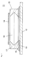
- Fig. 1 is a schematic cross-sectional view showing a structure of a conventional semiconductor device.
- a semiconductor device 11 has a lower surface of a semiconductor element 15 adhered to a die bonding pad 13 arranged on a substrate 12 like a printed wiring board using a die bonding resin 16 (silicon resin).
- the semiconductor element 15 has a diaphragm 14 laminated on the upper surface of a base 17, where the diaphragm 14 has the four corners fixed to the upper surface of the base 17, and a cavity 18 vertically passes through the base 17 so as not to inhibit the displacement or the vibration of the diaphragm 14.
- the upper half of the cavity 18 is a truncated pyramid shape, and the lower half is a reversed truncated pyramid shape, but the entire cavity 18 may be a truncated pyramid shape or a reversed truncated pyramid shape.
- the semiconductor device in which the semiconductor element is die bonded on the substrate like the printed wiring board includes a microphone disclosed in patent document 1, and the like.
- the die bonding resin 16 in the melted state is applied to the die bonding pad 13, the semiconductor element 15 is placed over the die bonding pad 13, and then the die bonding resin 16 is cured to fix the semiconductor element 15 to the substrate 12.
- the die bonding resin 16 in the melted state is sometimes taken up to the upper surface of the base 17. If the die bonding resin 16 is taken up, the die bonding resin 16 enters the gap between the diaphragm 14 and the upper surface of the base 17 and cures thereat, whereby the die bonding resin 16 may fix the diaphragm 14 to the base 17 or may enter the gap between the diaphragm 14 and the base 17 and become a foreign substance.
- the diaphragm 14 If the diaphragm 14 is fixed to the base 17, the diaphragm 14 cannot vibrate a defined amount and the semiconductor element 15 cannot obtain a predetermined sensitivity If the die bonding resin 16 is sandwiched between the diaphragm 14 and the base 17 as a foreign substance, the vibration characteristics of the semiconductor element 15 change. The failure thus occurs in the semiconductor device 11 and the yield of the semiconductor device 11 lower.
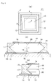
- Figs. 2 and 3 are views for describing the causes.
- Fig. 2A is a schematic plan view of the semiconductor device 11.
- Fig. 2B is an enlarged cross-sectional view taken along line X-X of Fig. 2A , and shows a cross-section of the semiconductor device 11 seen from a diagonal direction.
- Fig 2C is an enlarged cross-sectional view taken along line Y-Y of Fig. 2A , and shows a cross-section of the semiconductor device 11 seen from a diagonal direction.
- Fig. 3 shows a state in which the die bonding resin 16 rides up the wall surface of the cavity 18.
- the die bonding resin 16 (silicon resin) has satisfactory wetting property with respect to the base 17 made of semiconductor material such as Si, and thus the force F1 of riding up the through the wall surface 19 of the cavity 18 acts on the die bonding resin 16.
- the force of riding up the die bonding resin 16 acts on a valley section 20 where the wall surface 19 and the wall surface 19 cross from each wall surface 19 on both sides of the valley section 20, and a force of pushing up the die bonding resin 16 also acts by the capillary action as a narrow gap forms at the valley section 20.
- a large force F2 of riding up the die bonding resin 16 acts at the valley section 20 compared to the wall surface 19, and the die bonding resin 16 rides up to a higher position at the valley section 20.
- the height (distance) the die bonding resin 16 rides up the wall surface is determined by (1) surface tension that acts on the die bonding resin, (2) easiness in wetting of the wall surface, and (3) density of the die bonding resin.
- the die bonding resin 16 in the melted state rides up along the valley section 20, as shown with a broken line arrow in Fig. 2B , enters the gap between the diaphragm 14 and the base 17 from the valley section 20 as shown in Fig. 2C , and further spreads along the gap between the diaphragm 14 and the base 17.
- the diaphragm 14 fixes to the base 17 by the die bonding resin 16, or the die bonding resin 16 becomes a foreign substance thereby narrowing the gap between the diaphragm 14 and the base 17, and causing problems.
- the height or the amount the die bonding resin 16 rides up the valley section 20 changes depending on the elapsed time after the application and the application amount of the die bonding resin 16, and thus, consideration is made to reduce the application amount of the die bonding resin 16, or to reduce the time from when the die bonding resin 16 is applied until cured so that the above mentioned problems are unlikely to occur.
- the thickness of the die bonding resin 16 sandwiched between the die bonding pad 13 and the semiconductor element 15 becomes thin, and thus the action of alleviating the external impact on the semiconductor element 15 with the die bonding resin 16 may not be sufficiently obtained or the mounting strength of the semiconductor element 15 may lower.
- the manufacturing cost is high since a great number of semiconductor devices 11 cannot be processed all together, and the semiconductor device 11 needs to be transferred to a heating furnace to cure the die bonding resin 16 by a small number at a time. These methods are thus not practical.
- a semiconductor device includes a semiconductor element in which a cavity having a polygonal horizontal cross-section penetrates vertically through a base and a diaphragm is arranged on the base to cover the cavity, and a substrate formed with a die bonding pad, a lower surface of the semiconductor element being adhered on the die bonding pad with a die bonding resin; wherein the die bonding pad is formed so as not to contact a lower end of a valley section formed when a wall surface and a wall surface intersect at an inner peripheral surface of the cavity of the semiconductor element.
- the die bonding pad is formed so as not to contact the lower end of the valley section, and thus the die bonding resin does not touch the lower end of the valley section even if spread over the upper surface of the die bonding pad when the die bonding resin in the melted state is applied on the die bonding pad and the lower surface of the semiconductor element is overlapped thereon. Therefore, drawback in that the die bonding resin enters from the lower end of the valley section and rises up the cavity along the valley section thus fixing the diaphragm of entering the gap under the diaphragm and becoming a foreign substance can be prevented.
- the substrate is a printed substrate
- the die bonding pad is formed to include a conductor pattern of the printed substrate; and the conductor pattern is removed in a region (hereinafter referred to as valley section facing region) facing the lower end of the valley suction. If the substrate is a printed substrate, an opening can be formed in the conductor pattern by removing the conductor pattern in the valley section facing region, so that the die bonding resin can be prevented from rising up along the valley section.
- At least one part of a surface of an outer peripheral portion of the conductor pattern removed region of the conductor pattern is formed by an inorganic material such as Cu and Au.
- the inorganic material particularly Cu and Au does not have satisfactory wetting property with the die bonding resin, and thus the die bonding resin flowed towards the valley section facing region can be stopped at the portion formed with the inorganic material by forming at least one part of the surface of the outer peripheral portion of the conductor pattern removed region with an inorganic material such as Cu and Au, and the die bonding resin can be prevented from flowing into the conductor pattern removing region and contacting the lower end of the valley section.
- an outer peripheral edge of the die bonding pad is positioned on an outer side than an outer peripheral edge of the lower surface of the semiconductor element.
- the die bonding resin between the die bonding pad and the lower surface of the semiconductor element easily flows to the outer side of the semiconductor element since the die bonding pad is spread to the outer side than the semiconductor element.
- the die bonding resin that flows to the inner side of the semiconductor element reduces by such amount, and the die bonding resin is less likely to contact the wall surface of the cavity.
- the lower surface of the semiconductor element has an entire surface excluding a region in the vicinity of the lower end of the valley section adhered to the die bonding pad. According to such aspect, the adhering area of the semiconductor element can be increased since the lower surface of the semiconductor element is adhered with the entire surface excluding the region in the vicinity of the lower end of the valley section, and hence the adhering strength of the semiconductor element can be enhanced and the buffering effect by the die bonding resin can be enhanced.
- the means for solving the problems of the invention may appropriately combine the configuring elements described above, and the present invention enables a great number of variations from the combinations of the configuring elements.
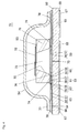
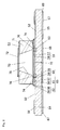
- Fig. 4 is a cross-sectional view showing a structure of a semiconductor device 51 according to a first embodiment of the present invention, and shows the cross-section in the diagonal direction of a substrate 52.
- Fig. 5 is a plan view of the substrate 52 used in the semiconductor device 51, and also shows one part thereof in an enlarged manner.
- the semiconductor device 51 shown here has a semiconductor element 53 mounted on an upper surface of the substrate 52, and the semiconductor element 53 accommodated in a package (Faraday cage) including the substrate 52 and a conductive cap 54,
- the substrate 52 is configured by a printed board, where a conductor pattern 56 (mental foil) of copper foil, and the like is stacked on substantially the entire surface of the upper surface of a substrate core material 55 (prepreg), as shown in Fig. 4 .
- a conductor pattern 69 (metal foil) of Cu and the like is also stacked on substantially the entire surface of the lower surface of the substrate core material 55, where an extraction electrode 67 and a rear surface side ground pattern 68 are formed by patterning the conductor pattern 69.
- the conductor pattern 56 on the upper surface is electrically connected to the rear surface side ground pattern 68 through the lower through a through-hole 70.
- the extraction electrode 67 and the rear surface side ground pattern 68 are patterns for solder mounting to the substrate (e.g., mother board for portable telephone) for mounting the semiconductor device 51.
- a first solder resist region 59 of a square shape in which the surface of the conductor pattern 56 is covered with a solder resist 57 is formed at a central part of the substrate 52.
- An inner peripheral side plated region 60 applied with an inorganic material layer 58 in which an inorganic material such as Cu and Au is plated on the surface of the conductor pattern 56 is formed to an annular shape on the outer side of the first solder resist region 59.
- a second solder resist region 61 of an annular shape in which the surface of the conductor pattern 56 is covered with the solder resist 57 is formed on the outer side of the inner peripheral side plated region 60.
- An outer peripheral side plated region 62 in which the inorganic material layer 58 including an inorganic material such as Cu and Au is applied on the surface of the conductor pattern 56 is formed to an annular shape on the outer side of the second solder resist region 61. Furthermore, a third solder resist region 63 of an annular shape in which the surface of the conductor pattern 56 is covered with the solder resist 57 is formed on the outer side of the outer peripheral side plated region 62. The region on the outer side of the third solder resist region 63 is a ground electrode portion 64 where the conductor pattern 56 is exposed.
- the solder resist 57 for protecting the conductor pattern 56 is obtained by applying the solder resist in the melted state to the surface of the surface of the substrate 52 by screen printing at an even thickness, and then heating to be cured.
- the solder resist is used as the covering member, but a silk pattern, and the like may be used. Since the copper foil is generally used for the conductor pattern 56 of the substrate 52, Au is desirably used for the inorganic material layer 58 of the inner peripheral side plated region 60 and the outer peripheral side plated region 62.
- the electrode pads 66a, 66b are arranged by exposing the conductor pattern 56 at one part of the third solder resist region 63.
- the electrode pads 66a, 66b are separated from the conductor pattern 56 of the third solder resist region 63 and electrically separated, and are electrically connected to the extraction electrode 67 of the rear surface of the substrate 52 through the through-hole (not shows),
- the semiconductor element 53 includes various types of sensing sensor chip (e.g., acoustic sensor, pressure sensor, etc.) including a diaphragm, and is an acoustic sensor (or transducer for converting acoustic vibration to electric energy) for detecting the acoustic vibration in the present embodiment.
- the semiconductor element 53 has a diaphragm 72 for sensing the acoustic vibration attached to the upper surface of the base 71 formed by processing the Si substrate, and the like, and detects the displacement of the diaphragm 72 due to acoustic vibration by electrostatic method and the like.
- a cavity73 having a square frustum shape is formed on the base 71 on the lower side of the diaphragm 72, and the cavity 73 penetrates the base 71 vertically.
- the cavity 73 is not limited to a square frustum shape as long as it penetrates vertically with a horizontal cross-section of a multiangular shape, and may be a polygonal frustum shape such as a triangular frustum shape or a pentagular frustum shape.
- the upper part of the cavity 73 may be a polygonal frustum shape and the lower part may be a reversed polygonal frustum shape.
- the diaphragm 72 has four corners fixed to the upper surface of the base 71, where a gap (vent hole) is formed between the lower surface of the diaphragm 72 and the upper surface of the base 71 at four sides on the outer periphery excluding the four corners.
- the lower surface of the semiconductor element 53 is a square ring shape surrounding the cavity 73, and is adhered and fixed on the die bonding pad 65 of the substrate 52 by the die bonding resin 74.
- An adhesive resin such as silicon resin having flexibility is used for the die bonding resin 74, where the die bonding resin 74 applied to a transfer pin (stamper) is transferred onto the die bonding pad 65, then the semiconductor element 53 is placed thereon and pushed with an even force, and the die bonding resin 74 is heated and cured to fix the semiconductor element 53.
- the die bonding resin 74 also acts to shield and buffer the extra force from the external environment other than to fix the semiconductor element 53.
- the terminal of the semiconductor element 53 and the electrode pads 66a, 66b are wire connected by a bonding wire (not shown), and hence the terminal of the semiconductor element 53 is electrically conducted to the extraction electrode 67 at the lower surface.
- the die bonding pad 65 is formed by the inner peripheral side plated region 60, the second solder resist region 61, and the outer peripheral side plated region 62.
- the positions of the inner peripheral end and the outer peripheral end of the lower surface of the semiconductor element 53 mounted on the upper surface of the substrate 52 are respectively indicated with a broken line.
- the inner peripheral end of the lower surface of the semiconductor element 53 substantially coincides with the inner peripheral end of the die bonding pad 65 (inner peripheral end of inner peripheral side plated region 60), and the outer peripheral end of the die bonding pad 65 (outer peripheral end of outer peripheral side plated region 62) is positioned on the outer side than the outer peripheral end of the lower surface of the semiconductor element 53.
- the opening 76 is formed excluding the die bonding pad 65 (conduct pattern 56) by etching, and the substrate core material 55 is exposed at the opening 65.
- the opening 76 has a square shape in Fig. 5 , but the shape of the opening 76 is not limited to a square and may be a circle or a polygonal etc. other than a square.
- the size of the opening 76 merely needs to have a length of one side of about 0.20 mm.
- the mounting accuracy of when mounting the semiconductor element 53 on the substrate 52 is ⁇ 0.05 mm, and thus a gap of at least 0.05 mm can be ensured between the lower end of the valley section 75 and the edge of the opening 76 if the dimension of the opening 76 has one side of 0.20 mm.
- the conductive cap 54 is formed to a cap shape by a metal material having small specific resistance, and a space for accommodating the semiconductor element 53 and the like is formed at the lower surface.
- a flange 77 extending substantially horizontally is formed over the entire periphery at the lower end of the conductive cap 54.
- the conductive cap 54 is mounted on the substrate 52 so as to cover the semiconductor element 53, and the like, where the lower surface of the flange 77 is joined and fixed to the ground electrode portion 64 by a conductive joining member 78 and electrically connected to the ground electrode portion 64 by the conductivity of the conductive joining member 78.
- the conductive cap 54 thus becomes the same potential (ground potential) as the rear surface side ground pattern 68 of the lower surface.
- a material such as conductive epoxy resin (e.g., epoxy resin containing silver filler), solder, and the like is used for the conductive joining member 78.
- the semiconductor element 53 to be mounted is an acoustic sensor
- a hole (not shown) for passing the acoustic vibration may be formed at the vertex of the conductive cap 54.
- the package including the conductive cap 54 and the substrate 52 may have a sealed structure depending on the type of semiconductor element 53 to accommodate. For instance, if dust, light, and the like from the outside are to be shielded, the semiconductor element 53 and the like may be covered with the package, where the package desirably has air tightness if humidity resistance and chemical resistance are required although air tightness is not necessarily required.
- the surface of the conductor pattern 56 is covered with the solder resist 57 in the second solder resist region 61 between the inner peripheral side plated region 60 and the outer peripheral side plated region 62 at the die bonding pad 65.
- the die bonding resin 74 such as silicon resin has higher adhering strength with respect to the solder resist than with respect to the inorganic material such as Cu and Au, and thus the adhering strength of the semiconductor element 53 by the die bonding resin 74 becomes higher by forming the solder resist 57 at one part of the die bonding pad 65.
- the inner peripheral side plated region 60 and the outer peripheral side plated region 62 covered with the inorganic material layer 58 having unsatisfactory wetting property with respect to the die bonding resin are formed at the inner peripheral part and the outer peripheral part of the die bonding pad 65, and hence the die bonding resin 74 can be prevented from leaking out to the inner peripheral side and the outer peripheral side of the die bonding pad 65.
- the reason therefor is as follows.
- a flexible resin such as silicon resin is used for the die bonding resin 74 to alleviate the factors of characteristic fluctuation such as external impact, which resin has a property of being easy to flow.
- the resin such as silicon resin has satisfactory wetting property and small contact angle with respect to the solder resist, which is the same organic maternal, Furthermore, the solder resist formed on the conductor pattern 56 is less likely to have the end face formed to a right angle and tends to be rounded.
- the contact angle ⁇ of when the die bonding resin 74 is applied becomes small, and consequently, the applied die bonding resin 74 easily flows out from the end of the die bonding pad 65, and the flow-out amount increases with time once the die bonding resin 74 starts to flow out.
- the resin such as silicon resin has unsatisfactory wetting property and large contact angle with respect to the inorganic material. Furthermore, the inorganic material tends to have the end face easily formed to a right angle compared to the solder resist. Therefore, if the surface of the inner peripheral part and the outer peripheral part of the die bonding pad 65 is configured by the inorganic material, the contact angle ⁇ of when the die bonding resin 74 is applied becomes large and the die bonding resin 74 becomes a spherical shape at the edge of the die bonding pad 65, and hence the applied die bonding resin 74 is less likely to flow out to the outer peripheral side or the inner peripheral side from the end of the die bonding pad 65.
- the die bonding resin 74 is inhibited from flowing out from the die bonding pad 65, the phenomenon in which the die bonding resin 74 that flowed out covers one part of the ground electrode portion 64 thereby inhibiting the joining of the conductive cap 54 to the ground electrode portion 64, and lowering the shielding property of the high frequency noise can be prevented.
- the thickness of die bonding resin 74 between the semiconductor element 53 and the die bonding pad 65 becomes thin with increase in the flow-out amount, but the variation in the thickness of the die bonding resin 74 can be reduced by managing the application amount of the die bonding resin 74 since the flow-out of the die bonding resin 74 can be prevented according to the present embodiment.
- the joining strength of the semiconductor element 53 becomes even
- the capacity of the cavity73 becomes even
- the elasticity of the die bonding resin 74 becomes even
- the quality of the semiconductor device 51 stabilizes.
- the thickness of the die bonding resin 74 at the lower surface of the semiconductor element 53 can be increased, and the effect of shielding redundant external force with the die bonding resin 74 can be further enhanced.
- the opening 76 is provided by removing the die bonding pad 65 (conductor pattern 56) in the region (region facing valley section) facing the lower end of the valley section 75, and thus the possibility the die bonding resin 74 applied to the die bonding pad 65 touches the lower end of the valley section 75 is small.
- the die bonding resin 74 can be prevented from entering the valley section 75 from the lower end of the valley section 75, rising up the valley section 75 and reaching the upper surface of the base 71.
- the die bonding resin 74 that attempts to flow towards the opening 76 is stopped by the inorganic material layer 58.
- the base 71 is formed from Si and has satisfactory wetting property with the die bonding resin 74 such as silicon resin, and thus the die bonding resin 74 accumulated at the distal end of the inner peripheral side plated region 60 rides up to the upper side along the outer peripheral side surface of the base 71 and forms a large resin fillet.
- the die bonding resin 74 that flowed towards the inner peripheral side of the die bonding pad 65 is inhibited from running out or flowing into the opening 76.
- the die bonding resin 74 that ran out or flowed out into the opening 76 is thus prevented from touching the lower end of the valley section 75 and running up the valley section 75.
- the entire periphery of the opening 76 is desirably surrounded with the inorganic material layer 58, but the inorganic material layer 58 may be formed at the periphery of the opening 76 only in the direction the die bonding resin 74 flows, as shown in Fig. 5 , in the present embodiment.
- the outer peripheral end of the die bonding pad 65 is positioned on the outer side than the outer peripheral end at the lower surface of the semiconductor element 53, and the outer peripheral end at the lower surface of the semiconductor element 53 is on the second solder resist region 61, and thus die bonding resin 74 is pulled towards the outer peripheral side than the inner peripheral side and thus easily runs out to the outer peripheral side.
- the amount of die bonding resin 74 flowing to the inner peripheral side where the opening 76 is formed can be reduced, whereby the die bonding resin 74 is less likely to run out or flow out into the opening 76 and the die bonding resin 74 can be prevented from touching the lower end of the valley section 75 and running up the valley section 75.
- the die bonding resin 74 in the melted state thus does not touch the lower end of the valley section 75 and run up the valley section 75, so that the diaphragm 72 is prevented from getting fixed to the base 71 by the die bonding resin 74 or being sandwiched between the diaphragm 72 and the base 71 as a foreign substance thereby inhibiting vibration and displacement.
- the Faraday cage is configured by a substrate 52 including the rear surface side ground pattern 68 and the conductor pattern 56 ground connected with the conductive cap 54 connected to the ground, and hence the semiconductor element 53 can be blocked from external high frequency noise and the influence oaf the semiconductor element 53 by external noise can be reduced.
- the warp of the substrate 52 due to temperature change, and the like can be prevented since substantival the entire surface of both front and rear surfaces of the substrate 52 are covered with a conductor pattern.
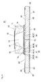
- Fig. 6 is a cross-sectional view showing a structure of a semiconductor device 81 according to a second embodiment of the present invention, and shows a state before attaching the conductive cap 54.
- Fig. 7 is a plan view of the substrate 52 used in the semiconductor device 81, and also shows one part thereof in an enlarged manner.
- the third solder resist region 63 in the first embodiment is removed to arrange a groove portion 82, and the substrate core material 55 is exposed in the groove portion 82.
- the inner peripheral end of the inner peripheral side plated region 60 is positioned on the inner side than the inner peripheral end (edge of cavity 73) at the lower surface of the semiconductor element 53, so that the entire periphery of the opening 76 is surrounded with the inner peripheral side plated region 60.
- the surface of the inner peripheral side plated region 60 is formed by the inorganic material layer 58 which has unsatisfactory wetting property with respect to the die bonding resin 74 and which end face tends to become a right angle, and hence the die bonding resin 74 is stopped at the entire periphery of the opening 76 and is more unlikely to flow into the opening 76, and the possibility of the die bonding resin 75 touching the lower end of the valley section 75 becomes smaller.
- Fig. 8 is a cross-sectional view showing a structure of a variant of the second embodiment, and shows a state before attaching the conductive cap 54.
- the substrate core material 55 is omitted at the bottom surface of the opening 76 to arrange an excavated portion 83. Since the excavated portion 83 is formed in the opening 76, the depth of the opening 76 becomes deeper and the die bonding resin 74 is less likely to touch the lower end of the valley section 75 in the unlikely event the die bonding resin 74 flows into the opening 76, whereby the possibility the die bonding resin 74 runs up along the valley section 75 becomes smaller.
- the aspect of deepening the opening 76 can be applied to embodiments other than the second embodiment.
- Fig. 9 is a cross-sectional view showing a structure of a semiconductor device 91 according to a third embodiment of the present invention, and shows a state before attaching the conductive cap 54.
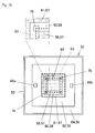
- Fig. 10 is a plan view of the substrate 52 used in the semiconductor device 91, and also shows one part thereof in an enlarged manner.
- the outer peripheral side plated region 62 in the second embodiment is removed to enlarge the groove portion 82, and the outer peripheral end of the second solder resist region 61 is substantially coincided with the outer peripheral end of the lower surface of the semiconductor element 53.
- the die bonding resin 74 that flowed out to the outer side is less likely to flow to the ground electrode portion 64 since the groove portion 82 can be widened.
- Fig. 1 is a cross-sectional view showing a structure of a semiconductor device 101 according to a fourth embodiment of the present invention, and shows a state before attaching the conductive cap 54.
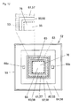
- Fin, 12 sis a plan view of the substrate 52 used in the semiconductor device 101, and also shows one part thereof in an enlarged manner.
- the first solder resist region 59 in the second embodiment is removed to expose the substrate core material 55.
- the inner peripheral end of the inner peripheral side plated region 60 is positioned on the outer peripheral side than the inner peripheral end (edge off cavity 73) of the lower surface of the semiconductor element 53 to form the opening 76 entirety on the inner side than the inner peripheral side plated region 60 including the region facing the valley section.
- the entire inner side of the die bonding pad 65 is the opening 76, and the effect of stopping the die bonding resin 74 with the inner peripheral end of the die bonding pad 65 (or inner peripheral side plated region 60) is enhanced by removing the first solder resist region 59, and thus the effect of preventing the die bonding resin 74 from running up the valley section 75 becomes higher.
Landscapes
- Engineering & Computer Science (AREA)
- Physics & Mathematics (AREA)
- Microelectronics & Electronic Packaging (AREA)
- Manufacturing & Machinery (AREA)
- Acoustics & Sound (AREA)
- Signal Processing (AREA)
- Pressure Sensors (AREA)
- Die Bonding (AREA)
- Structures Or Materials For Encapsulating Or Coating Semiconductor Devices Or Solid State Devices (AREA)
- Electrostatic, Electromagnetic, Magneto- Strictive, And Variable-Resistance Transducers (AREA)
- Health & Medical Sciences (AREA)
- Electromagnetism (AREA)
- Toxicology (AREA)
Abstract
Description
- The present invention rotates to semiconductor devices. Specifically, the present invention relates to a semiconductor device in which a semiconductor element such as a sensor chip including a diaphragm is mounted on a substrate.
-
Fig. 1 is a schematic cross-sectional view showing a structure of a conventional semiconductor device. Asemiconductor device 11 has a lower surface of asemiconductor element 15 adhered to adie bonding pad 13 arranged on asubstrate 12 like a printed wiring board using a die bonding resin 16 (silicon resin). Thesemiconductor element 15 has adiaphragm 14 laminated on the upper surface of abase 17, where thediaphragm 14 has the four corners fixed to the upper surface of thebase 17, and acavity 18 vertically passes through thebase 17 so as not to inhibit the displacement or the vibration of thediaphragm 14. In the illustrated example, the upper half of thecavity 18 is a truncated pyramid shape, and the lower half is a reversed truncated pyramid shape, but theentire cavity 18 may be a truncated pyramid shape or a reversed truncated pyramid shape. The semiconductor device in which the semiconductor element is die bonded on the substrate like the printed wiring board includes a microphone disclosed in patent document 1, and the like. - In the assembly step of
such semiconductor device 11, thedie bonding resin 16 in the melted state is applied to thedie bonding pad 13, thesemiconductor element 15 is placed over thedie bonding pad 13, and then thedie bonding resin 16 is cured to fix thesemiconductor element 15 to thesubstrate 12. - When die bonding the
semiconductor element 15 to thesubstrate 12 in such manner, thedie bonding resin 16 in the melted state is sometimes taken up to the upper surface of thebase 17. If thedie bonding resin 16 is taken up, thedie bonding resin 16 enters the gap between thediaphragm 14 and the upper surface of thebase 17 and cures thereat, whereby thedie bonding resin 16 may fix thediaphragm 14 to thebase 17 or may enter the gap between thediaphragm 14 and thebase 17 and become a foreign substance. If thediaphragm 14 is fixed to thebase 17, thediaphragm 14 cannot vibrate a defined amount and thesemiconductor element 15 cannot obtain a predetermined sensitivity If thedie bonding resin 16 is sandwiched between thediaphragm 14 and thebase 17 as a foreign substance, the vibration characteristics of thesemiconductor element 15 change. The failure thus occurs in thesemiconductor device 11 and the yield of thesemiconductor device 11 lower. - The inventors of the present invention examined the phenomenon in which the
die bonding resin 16 is taken up and found that it is caused by the following causes.Figs. 2 and3 are views for describing the causes.Fig. 2A is a schematic plan view of thesemiconductor device 11.Fig, 2B is an enlarged cross-sectional view taken along line X-X ofFig. 2A , and shows a cross-section of thesemiconductor device 11 seen from a diagonal direction.Fig 2C is an enlarged cross-sectional view taken along line Y-Y ofFig. 2A , and shows a cross-section of thesemiconductor device 11 seen from a diagonal direction.Fig. 3 shows a state in which the die bonding resin 16 rides up the wall surface of thecavity 18. - The die bonding resin 16 (silicon resin) has satisfactory wetting property with respect to the
base 17 made of semiconductor material such as Si, and thus the force F1 of riding up the through thewall surface 19 of thecavity 18 acts on thedie bonding resin 16. In particular, the force of riding up thedie bonding resin 16 acts on avalley section 20 where thewall surface 19 and thewall surface 19 cross from eachwall surface 19 on both sides of thevalley section 20, and a force of pushing up thedie bonding resin 16 also acts by the capillary action as a narrow gap forms at thevalley section 20. As a result, a large force F2 of riding up thedie bonding resin 16 acts at thevalley section 20 compared to thewall surface 19, and thedie bonding resin 16 rides up to a higher position at thevalley section 20. The height (distance) the die bonding resin 16 rides up the wall surface is determined by (1) surface tension that acts on the die bonding resin, (2) easiness in wetting of the wall surface, and (3) density of the die bonding resin. - Due to such causes, the
die bonding resin 16 in the melted state rides up along thevalley section 20, as shown with a broken line arrow inFig. 2B , enters the gap between thediaphragm 14 and thebase 17 from thevalley section 20 as shown inFig. 2C , and further spreads along the gap between thediaphragm 14 and thebase 17. As a result, thediaphragm 14 fixes to thebase 17 by thedie bonding resin 16, or thedie bonding resin 16 becomes a foreign substance thereby narrowing the gap between thediaphragm 14 and thebase 17, and causing problems. - The height or the amount the
die bonding resin 16 rides up thevalley section 20 changes depending on the elapsed time after the application and the application amount of thedie bonding resin 16, and thus, consideration is made to reduce the application amount of thedie bonding resin 16, or to reduce the time from when thedie bonding resin 16 is applied until cured so that the above mentioned problems are unlikely to occur. However, in the method of reducing the application amount of thedie bonding resin 16, the thickness of thedie bonding resin 16 sandwiched between thedie bonding pad 13 and thesemiconductor element 15 becomes thin, and thus the action of alleviating the external impact on thesemiconductor element 15 with thedie bonding resin 16 may not be sufficiently obtained or the mounting strength of thesemiconductor element 15 may lower. In the method of reducing the time until curing thedie bonding resin 16, the manufacturing cost is high since a great number ofsemiconductor devices 11 cannot be processed all together, and thesemiconductor device 11 needs to be transferred to a heating furnace to cure thedie bonding resin 16 by a small number at a time. These methods are thus not practical. -
- Patent Document 1:
US Patent Specification No. 7,166,910 (Fig. 28) - In view of the technical problems described above, it is an object of the present invention to provide a semiconductor device capable of preventing the die bonding resin from riding up the cavity through the valley section of the cavity arranged in the semiconductor element.
- In accordance with one aspect of the present invention, a semiconductor device according to the present invention includes a semiconductor element in which a cavity having a polygonal horizontal cross-section penetrates vertically through a base and a diaphragm is arranged on the base to cover the cavity, and a substrate formed with a die bonding pad, a lower surface of the semiconductor element being adhered on the die bonding pad with a die bonding resin; wherein the die bonding pad is formed so as not to contact a lower end of a valley section formed when a wall surface and a wall surface intersect at an inner peripheral surface of the cavity of the semiconductor element.
- In the semiconductor device of the present invention, the die bonding pad is formed so as not to contact the lower end of the valley section, and thus the die bonding resin does not touch the lower end of the valley section even if spread over the upper surface of the die bonding pad when the die bonding resin in the melted state is applied on the die bonding pad and the lower surface of the semiconductor element is overlapped thereon. Therefore, drawback in that the die bonding resin enters from the lower end of the valley section and rises up the cavity along the valley section thus fixing the diaphragm of entering the gap under the diaphragm and becoming a foreign substance can be prevented.
- In one aspect of the semiconductor device according to the present invention, the substrate is a printed substrate, the die bonding pad is formed to include a conductor pattern of the printed substrate; and the conductor pattern is removed in a region (hereinafter referred to as valley section facing region) facing the lower end of the valley suction. If the substrate is a printed substrate, an opening can be formed in the conductor pattern by removing the conductor pattern in the valley section facing region, so that the die bonding resin can be prevented from rising up along the valley section.
- In another aspect of the semiconductor device according to the present invention, at least one part of a surface of an outer peripheral portion of the conductor pattern removed region of the conductor pattern is formed by an inorganic material such as Cu and Au. The inorganic material particularly Cu and Au does not have satisfactory wetting property with the die bonding resin, and thus the die bonding resin flowed towards the valley section facing region can be stopped at the portion formed with the inorganic material by forming at least one part of the surface of the outer peripheral portion of the conductor pattern removed region with an inorganic material such as Cu and Au, and the die bonding resin can be prevented from flowing into the conductor pattern removing region and contacting the lower end of the valley section.
- In another further aspect of the semiconductor device according to the present invention, an outer peripheral edge of the die bonding pad is positioned on an outer side than an outer peripheral edge of the lower surface of the semiconductor element. According to such aspect, the die bonding resin between the die bonding pad and the lower surface of the semiconductor element easily flows to the outer side of the semiconductor element since the die bonding pad is spread to the outer side than the semiconductor element. The die bonding resin that flows to the inner side of the semiconductor element reduces by such amount, and the die bonding resin is less likely to contact the wall surface of the cavity.
- In another further aspect of the semiconductor device according to the present invention, the lower surface of the semiconductor element has an entire surface excluding a region in the vicinity of the lower end of the valley section adhered to the die bonding pad. According to such aspect, the adhering area of the semiconductor element can be increased since the lower surface of the semiconductor element is adhered with the entire surface excluding the region in the vicinity of the lower end of the valley section, and hence the adhering strength of the semiconductor element can be enhanced and the buffering effect by the die bonding resin can be enhanced.
- The means for solving the problems of the invention may appropriately combine the configuring elements described above, and the present invention enables a great number of variations from the combinations of the configuring elements.
-
-
Fig. 1 is a schematic cross-sectional view of a conventional semiconductor device. -
Fig. 2A is a schematic plan view of the semiconductor device,Fig. 2B is an enlarged cross-sectional view taken along line X-X ofFig. 2A, and Fig. 2C is an enlarged cross-sectional view taken along line Y-Y ofFig. 2A . -
Fig. 3 is a view describing the reasons the die bonding resin runs up along a valley line. -
Fig. 4 is a cross-sectional view of a semiconductor device according to a first embodiment of the present invention. - Fin. 5 is a plan view of a printed wiring board used in the semiconductor device of the first embodiment.
-
Fig. 6 is a cross-sectional view in which one part of the semiconductor device according to a second embodiment of the present invention is omitted. -
Fig. 7 is a plan view of the printed wiring board used in the semiconductor device of the second embodiment. -
Fig. 8 is a cross-sectional view in which one part of a semiconductor device according to a variant of the second embodiment is omitted. -
Fig. 9 is a cross-sectional view in which one part of a semiconductor device according to a third embodiment of the present invention is omitted. -
Fig. 10 is a plan view of a printed wiring board used in the semiconductor device of the third embodiment. -
Fig. 11 is a cross-sectional view in which one part of a semiconductor device according to a fourth embodiment of the present invention is omitted. -
Fig. 12 is a plan view of a printed wiring board used in the semiconductor device of the fourth embodiment. - Suitable embodiments of the present invention will be hereinafter described with reference to the accompanied drawings.
-
Fig. 4 is a cross-sectional view showing a structure of asemiconductor device 51 according to a first embodiment of the present invention, and shows the cross-section in the diagonal direction of asubstrate 52.Fig. 5 is a plan view of thesubstrate 52 used in thesemiconductor device 51, and also shows one part thereof in an enlarged manner. Thesemiconductor device 51 shown here has asemiconductor element 53 mounted on an upper surface of thesubstrate 52, and thesemiconductor element 53 accommodated in a package (Faraday cage) including thesubstrate 52 and aconductive cap 54, - The
substrate 52 is configured by a printed board, where a conductor pattern 56 (mental foil) of copper foil, and the like is stacked on substantially the entire surface of the upper surface of a substrate core material 55 (prepreg), as shown inFig. 4 . A conductor pattern 69 (metal foil) of Cu and the like is also stacked on substantially the entire surface of the lower surface of thesubstrate core material 55, where anextraction electrode 67 and a rear surfaceside ground pattern 68 are formed by patterning theconductor pattern 69. Theconductor pattern 56 on the upper surface is electrically connected to the rear surfaceside ground pattern 68 through the lower through a through-hole 70. Theextraction electrode 67 and the rear surfaceside ground pattern 68 are patterns for solder mounting to the substrate (e.g., mother board for portable telephone) for mounting thesemiconductor device 51. - As shown in
Fig. 5 , a first solder resistregion 59 of a square shape in which the surface of theconductor pattern 56 is covered with a solder resist 57 is formed at a central part of thesubstrate 52. An inner peripheral side platedregion 60 applied with aninorganic material layer 58 in which an inorganic material such as Cu and Au is plated on the surface of theconductor pattern 56 is formed to an annular shape on the outer side of the first solder resistregion 59. A second solder resistregion 61 of an annular shape in which the surface of theconductor pattern 56 is covered with the solder resist 57 is formed on the outer side of the inner peripheral side platedregion 60. An outer peripheral side platedregion 62 in which theinorganic material layer 58 including an inorganic material such as Cu and Au is applied on the surface of theconductor pattern 56 is formed to an annular shape on the outer side of the second solder resistregion 61. Furthermore, a third solder resistregion 63 of an annular shape in which the surface of theconductor pattern 56 is covered with the solder resist 57 is formed on the outer side of the outer peripheral side platedregion 62. The region on the outer side of the third solder resistregion 63 is aground electrode portion 64 where theconductor pattern 56 is exposed. - The solder resist 57 for protecting the
conductor pattern 56 is obtained by applying the solder resist in the melted state to the surface of the surface of thesubstrate 52 by screen printing at an even thickness, and then heating to be cured. In this embodiment, the solder resist is used as the covering member, but a silk pattern, and the like may be used. Since the copper foil is generally used for theconductor pattern 56 of thesubstrate 52, Au is desirably used for theinorganic material layer 58 of the inner peripheral side platedregion 60 and the outer peripheral side platedregion 62. - The
electrode pads conductor pattern 56 at one part of the third solder resistregion 63. Theelectrode pads conductor pattern 56 of the third solder resistregion 63 and electrically separated, and are electrically connected to theextraction electrode 67 of the rear surface of thesubstrate 52 through the through-hole (not shows), - The
semiconductor element 53 includes various types of sensing sensor chip (e.g., acoustic sensor, pressure sensor, etc.) including a diaphragm, and is an acoustic sensor (or transducer for converting acoustic vibration to electric energy) for detecting the acoustic vibration in the present embodiment. Thesemiconductor element 53 has adiaphragm 72 for sensing the acoustic vibration attached to the upper surface of the base 71 formed by processing the Si substrate, and the like, and detects the displacement of thediaphragm 72 due to acoustic vibration by electrostatic method and the like. A cavity73 having a square frustum shape is formed on thebase 71 on the lower side of thediaphragm 72, and thecavity 73 penetrates the base 71 vertically. Thecavity 73 is not limited to a square frustum shape as long as it penetrates vertically with a horizontal cross-section of a multiangular shape, and may be a polygonal frustum shape such as a triangular frustum shape or a pentagular frustum shape. Alternatively, the upper part of thecavity 73 may be a polygonal frustum shape and the lower part may be a reversed polygonal frustum shape. Thediaphragm 72 has four corners fixed to the upper surface of thebase 71, where a gap (vent hole) is formed between the lower surface of thediaphragm 72 and the upper surface of the base 71 at four sides on the outer periphery excluding the four corners. - The lower surface of the
semiconductor element 53 is a square ring shape surrounding thecavity 73, and is adhered and fixed on thedie bonding pad 65 of thesubstrate 52 by thedie bonding resin 74. An adhesive resin such as silicon resin having flexibility is used for thedie bonding resin 74, where thedie bonding resin 74 applied to a transfer pin (stamper) is transferred onto thedie bonding pad 65, then thesemiconductor element 53 is placed thereon and pushed with an even force, and thedie bonding resin 74 is heated and cured to fix thesemiconductor element 53. Thedie bonding resin 74 also acts to shield and buffer the extra force from the external environment other than to fix thesemiconductor element 53. The terminal of thesemiconductor element 53 and theelectrode pads semiconductor element 53 is electrically conducted to theextraction electrode 67 at the lower surface. - As shown in
Figs. 4 and5 , thedie bonding pad 65 is formed by the inner peripheral side platedregion 60, the second solder resistregion 61, and the outer peripheral side platedregion 62. InFig. 5 , the positions of the inner peripheral end and the outer peripheral end of the lower surface of thesemiconductor element 53 mounted on the upper surface of thesubstrate 52 are respectively indicated with a broken line. The inner peripheral end of the lower surface of thesemiconductor element 53 substantially coincides with the inner peripheral end of the die bonding pad 65 (inner peripheral end of inner peripheral side plated region 60), and the outer peripheral end of the die bonding pad 65 (outer peripheral end of outer peripheral side plated region 62) is positioned on the outer side than the outer peripheral end of the lower surface of thesemiconductor element 53. - At the position corresponding to the lower end of the
valley section 75 formed at the four corners of thecavity 73, theopening 76 is formed excluding the die bonding pad 65 (conduct pattern 56) by etching, and thesubstrate core material 55 is exposed at theopening 65. Theopening 76 has a square shape inFig. 5 , but the shape of theopening 76 is not limited to a square and may be a circle or a polygonal etc. other than a square. The size of theopening 76 merely needs to have a length of one side of about 0.20 mm. The mounting accuracy of when mounting thesemiconductor element 53 on thesubstrate 52 is ± 0.05 mm, and thus a gap of at least 0.05 mm can be ensured between the lower end of thevalley section 75 and the edge of theopening 76 if the dimension of theopening 76 has one side of 0.20 mm. - The
conductive cap 54 is formed to a cap shape by a metal material having small specific resistance, and a space for accommodating thesemiconductor element 53 and the like is formed at the lower surface. Aflange 77 extending substantially horizontally is formed over the entire periphery at the lower end of theconductive cap 54. - The
conductive cap 54 is mounted on thesubstrate 52 so as to cover thesemiconductor element 53, and the like, where the lower surface of theflange 77 is joined and fixed to theground electrode portion 64 by a conductive joiningmember 78 and electrically connected to theground electrode portion 64 by the conductivity of the conductive joiningmember 78. Theconductive cap 54 thus becomes the same potential (ground potential) as the rear surfaceside ground pattern 68 of the lower surface. A material such as conductive epoxy resin (e.g., epoxy resin containing silver filler), solder, and the like is used for the conductive joiningmember 78. - If the
semiconductor element 53 to be mounted is an acoustic sensor, a hole (not shown) for passing the acoustic vibration may be formed at the vertex of theconductive cap 54. The package including theconductive cap 54 and thesubstrate 52 may have a sealed structure depending on the type ofsemiconductor element 53 to accommodate. For instance, if dust, light, and the like from the outside are to be shielded, thesemiconductor element 53 and the like may be covered with the package, where the package desirably has air tightness if humidity resistance and chemical resistance are required although air tightness is not necessarily required. - As shown in
Fig. 5 , according to thesemiconductor device 51 configured as above, the surface of theconductor pattern 56 is covered with the solder resist 57 in the second solder resistregion 61 between the inner peripheral side platedregion 60 and the outer peripheral side platedregion 62 at thedie bonding pad 65. Thedie bonding resin 74 such as silicon resin has higher adhering strength with respect to the solder resist than with respect to the inorganic material such as Cu and Au, and thus the adhering strength of thesemiconductor element 53 by thedie bonding resin 74 becomes higher by forming the solder resist 57 at one part of thedie bonding pad 65. - In the
semiconductor device 51, the inner peripheral side platedregion 60 and the outer peripheral side platedregion 62 covered with theinorganic material layer 58 having unsatisfactory wetting property with respect to the die bonding resin are formed at the inner peripheral part and the outer peripheral part of thedie bonding pad 65, and hence thedie bonding resin 74 can be prevented from leaking out to the inner peripheral side and the outer peripheral side of thedie bonding pad 65. The reason therefor is as follows. - A flexible resin such as silicon resin is used for the
die bonding resin 74 to alleviate the factors of characteristic fluctuation such as external impact, which resin has a property of being easy to flow. The resin such as silicon resin has satisfactory wetting property and small contact angle with respect to the solder resist, which is the same organic maternal, Furthermore, the solder resist formed on theconductor pattern 56 is less likely to have the end face formed to a right angle and tends to be rounded. Thus, when the entire surface of thedie bonding resin 65 is covered with the solder resist 57, the contact angle θ of when thedie bonding resin 74 is applied becomes small, and consequently, the applied diebonding resin 74 easily flows out from the end of thedie bonding pad 65, and the flow-out amount increases with time once thedie bonding resin 74 starts to flow out. - The resin such as silicon resin has unsatisfactory wetting property and large contact angle with respect to the inorganic material. Furthermore, the inorganic material tends to have the end face easily formed to a right angle compared to the solder resist. Therefore, if the surface of the inner peripheral part and the outer peripheral part of the
die bonding pad 65 is configured by the inorganic material, the contact angle θ of when thedie bonding resin 74 is applied becomes large and thedie bonding resin 74 becomes a spherical shape at the edge of thedie bonding pad 65, and hence the applied diebonding resin 74 is less likely to flow out to the outer peripheral side or the inner peripheral side from the end of thedie bonding pad 65. - If the
die bonding resin 74 is inhibited from flowing out from thedie bonding pad 65, the phenomenon in which thedie bonding resin 74 that flowed out covers one part of theground electrode portion 64 thereby inhibiting the joining of theconductive cap 54 to theground electrode portion 64, and lowering the shielding property of the high frequency noise can be prevented. - If the
die bonding resin 74 flows out from thedie bonding pad 65, the thickness ofdie bonding resin 74 between thesemiconductor element 53 and thedie bonding pad 65 becomes thin with increase in the flow-out amount, but the variation in the thickness of thedie bonding resin 74 can be reduced by managing the application amount of thedie bonding resin 74 since the flow-out of thedie bonding resin 74 can be prevented according to the present embodiment. As a result, the joining strength of thesemiconductor element 53 becomes even, the capacity of the cavity73 becomes even, the elasticity of thedie bonding resin 74 becomes even, and the quality of thesemiconductor device 51 stabilizes. - Furthermore, since the flow-out of the
die bonding resin 74 can be prevented, the thickness of thedie bonding resin 74 at the lower surface of thesemiconductor element 53 can be increased, and the effect of shielding redundant external force with thedie bonding resin 74 can be further enhanced. - In the
semiconductor device 51 of the present embodiment, theopening 76 is provided by removing the die bonding pad 65 (conductor pattern 56) in the region (region facing valley section) facing the lower end of thevalley section 75, and thus the possibility thedie bonding resin 74 applied to the diebonding pad 65 touches the lower end of thevalley section 75 is small. Thus, thedie bonding resin 74 can be prevented from entering thevalley section 75 from the lower end of thevalley section 75, rising up thevalley section 75 and reaching the upper surface of thebase 71. - Since the
inorganic material layer 58 made of inorganic material such as Au having unsatisfactory wetting property with thedie bonding resin 74 and which end face easily becomes a right angle is formed at the periphery of theopening 76, thedie bonding resin 74 that attempts to flow towards the opening 76 is stopped by theinorganic material layer 58. Thebase 71 is formed from Si and has satisfactory wetting property with thedie bonding resin 74 such as silicon resin, and thus thedie bonding resin 74 accumulated at the distal end of the inner peripheral side platedregion 60 rides up to the upper side along the outer peripheral side surface of thebase 71 and forms a large resin fillet. As a result, thedie bonding resin 74 that flowed towards the inner peripheral side of thedie bonding pad 65 is inhibited from running out or flowing into theopening 76. Thedie bonding resin 74 that ran out or flowed out into theopening 76 is thus prevented from touching the lower end of thevalley section 75 and running up thevalley section 75. The entire periphery of theopening 76 is desirably surrounded with theinorganic material layer 58, but theinorganic material layer 58 may be formed at the periphery of theopening 76 only in the direction thedie bonding resin 74 flows, as shown inFig. 5 , in the present embodiment. - Furthermore, the outer peripheral end of the
die bonding pad 65 is positioned on the outer side than the outer peripheral end at the lower surface of thesemiconductor element 53, and the outer peripheral end at the lower surface of thesemiconductor element 53 is on the second solder resistregion 61, and thus diebonding resin 74 is pulled towards the outer peripheral side than the inner peripheral side and thus easily runs out to the outer peripheral side. Thus, the amount ofdie bonding resin 74 flowing to the inner peripheral side where theopening 76 is formed can be reduced, whereby thedie bonding resin 74 is less likely to run out or flow out into theopening 76 and thedie bonding resin 74 can be prevented from touching the lower end of thevalley section 75 and running up thevalley section 75. - The
die bonding resin 74 in the melted state thus does not touch the lower end of thevalley section 75 and run up thevalley section 75, so that thediaphragm 72 is prevented from getting fixed to thebase 71 by thedie bonding resin 74 or being sandwiched between thediaphragm 72 and the base 71 as a foreign substance thereby inhibiting vibration and displacement. - In the
semiconductor device 51, the Faraday cage is configured by asubstrate 52 including the rear surfaceside ground pattern 68 and theconductor pattern 56 ground connected with theconductive cap 54 connected to the ground, and hence thesemiconductor element 53 can be blocked from external high frequency noise and the influence oaf thesemiconductor element 53 by external noise can be reduced. - Furthermore, the warp of the
substrate 52 due to temperature change, and the like can be prevented since substantival the entire surface of both front and rear surfaces of thesubstrate 52 are covered with a conductor pattern. -
Fig. 6 is a cross-sectional view showing a structure of asemiconductor device 81 according to a second embodiment of the present invention, and shows a state before attaching theconductive cap 54.Fig. 7 is a plan view of thesubstrate 52 used in thesemiconductor device 81, and also shows one part thereof in an enlarged manner. In the embodiment, the third solder resistregion 63 in the first embodiment is removed to arrange agroove portion 82, and thesubstrate core material 55 is exposed in thegroove portion 82. Ifsuch groove portion 82 is formed, the effect of stopping thedie bonding resin 74 at the outer peripheral end of the die bonding pad 65 (or outer peripheral side plated region 62) becomes higher, and thedie bonding resin 74 is less likely to flow towards the outer side of thedie bonding pad 65 and attach to theground electrode portion 64. - As shown in
Fig. 7 , in the present embodiment, the inner peripheral end of the inner peripheral side platedregion 60 is positioned on the inner side than the inner peripheral end (edge of cavity 73) at the lower surface of thesemiconductor element 53, so that the entire periphery of theopening 76 is surrounded with the inner peripheral side platedregion 60. The surface of the inner peripheral side platedregion 60 is formed by theinorganic material layer 58 which has unsatisfactory wetting property with respect to the diebonding resin 74 and which end face tends to become a right angle, and hence thedie bonding resin 74 is stopped at the entire periphery of theopening 76 and is more unlikely to flow into theopening 76, and the possibility of thedie bonding resin 75 touching the lower end of thevalley section 75 becomes smaller. -
Fig. 8 is a cross-sectional view showing a structure of a variant of the second embodiment, and shows a state before attaching theconductive cap 54. In the variant, thesubstrate core material 55 is omitted at the bottom surface of theopening 76 to arrange an excavatedportion 83. Since the excavatedportion 83 is formed in theopening 76, the depth of theopening 76 becomes deeper and thedie bonding resin 74 is less likely to touch the lower end of thevalley section 75 in the unlikely event thedie bonding resin 74 flows into theopening 76, whereby the possibility thedie bonding resin 74 runs up along thevalley section 75 becomes smaller. - The aspect of deepening the
opening 76 can be applied to embodiments other than the second embodiment. -
Fig. 9 is a cross-sectional view showing a structure of asemiconductor device 91 according to a third embodiment of the present invention, and shows a state before attaching theconductive cap 54.Fig. 10 is a plan view of thesubstrate 52 used in thesemiconductor device 91, and also shows one part thereof in an enlarged manner. In the embodiment, the outer peripheral side platedregion 62 in the second embodiment is removed to enlarge thegroove portion 82, and the outer peripheral end of the second solder resistregion 61 is substantially coincided with the outer peripheral end of the lower surface of thesemiconductor element 53. According to such embodiment, thedie bonding resin 74 that flowed out to the outer side is less likely to flow to theground electrode portion 64 since thegroove portion 82 can be widened. -
Fig. 1 is a cross-sectional view showing a structure of asemiconductor device 101 according to a fourth embodiment of the present invention, and shows a state before attaching theconductive cap 54. Fin, 12 sis a plan view of thesubstrate 52 used in thesemiconductor device 101, and also shows one part thereof in an enlarged manner. In the embodiment, the first solder resistregion 59 in the second embodiment is removed to expose thesubstrate core material 55. The inner peripheral end of the inner peripheral side platedregion 60 is positioned on the outer peripheral side than the inner peripheral end (edge off cavity 73) of the lower surface of thesemiconductor element 53 to form theopening 76 entirety on the inner side than the inner peripheral side platedregion 60 including the region facing the valley section. In the embodiment, the entire inner side of thedie bonding pad 65 is theopening 76, and the effect of stopping thedie bonding resin 74 with the inner peripheral end of the die bonding pad 65 (or inner peripheral side plated region 60) is enhanced by removing the first solder resistregion 59, and thus the effect of preventing thedie bonding resin 74 from running up thevalley section 75 becomes higher. -
- 51, 81, 91, 101
- semiconductor device
- 52
- substrate
- 53
- semiconductor element
- 55
- substrate core material
- 56
- conductor pattern
- 57
- solder resist
- 58
- inorganic material layer
- 59
- first solder resist region
- 60
- inner peripheral side plated region
- 61
- second solder resist region
- 62
- outer peripheral side plated region
- 63
- third solder resist region
- 64
- ground electrode portion
- 65
- die bonding pad
- 71
- base
- 72
- diaphragm
- 73
- cavity
- 74
- die bonding resin
- 75
- valley section
- 76
- opening
Claims (5)
- A semiconductor device inducing a semiconductor element (53) in which a cavity (73) having a polygonal horizontal cross-section penetrates vertically through a base (71) and a diaphragm (72) is arranged on the base (71) to cover the cavity (73), and a substrate (52) formed with a die bonding pad (65), a lower surface of the semiconductor element (53) being adhered on the die bonding pad (65) with a die bonding resin (74); characterized in that
the die bonding pad (65) is formed so as not to contact a lower end of a valley section (75) formed when a wall surface and a wall surface intersect at an inner peripheral surface of the cavity (73) of the semiconductor element (53). - The semiconductor device according to claim 1, characterized in that
the substrate (52) is a printed substrate, the die bonding pad (65) being formed to include a conductor pattern of the printed substrate; and
the conductor pattern is removed in a region facing the lower end of the valley section (75). - The semiconductor device according to claim 2, characterized in that at least one part of a surface of an outer peripheral portion of the conductor pattern removed region of the conductor pattern is formed by an inorganic material such as Cu and Au.
- The semiconductor device according to claim 1, characterized in that an outer peripheral edge of the die bonding pad (65) is positioned on an outer side than an outer peripheral edge of the lower surface of the semiconductor element (53).
- The semiconductor device according to claim 1, characterized in that the lower surface of the semiconductor element (53) has an entire surface excluding a region in the vicinity of the lower end of the valley section (75) adhered to the die bonding pad (65).
Applications Claiming Priority (2)
| Application Number | Priority Date | Filing Date | Title |
|---|---|---|---|
| JP2008235736A JP4366666B1 (en) | 2008-09-12 | 2008-09-12 | Semiconductor device |
| PCT/JP2009/000728 WO2010029655A1 (en) | 2008-09-12 | 2009-02-20 | Semiconductor device |
Publications (3)
| Publication Number | Publication Date |
|---|---|
| EP2325875A1 true EP2325875A1 (en) | 2011-05-25 |
| EP2325875A4 EP2325875A4 (en) | 2014-08-06 |
| EP2325875B1 EP2325875B1 (en) | 2018-06-06 |
Family
ID=41443774
Family Applications (1)
| Application Number | Title | Priority Date | Filing Date |
|---|---|---|---|
| EP09812805.1A Not-in-force EP2325875B1 (en) | 2008-09-12 | 2009-02-20 | Semiconductor device |
Country Status (6)
| Country | Link |
|---|---|
| US (1) | US9363617B2 (en) |
| EP (1) | EP2325875B1 (en) |
| JP (1) | JP4366666B1 (en) |
| KR (1) | KR101166654B1 (en) |
| CN (1) | CN102124549B (en) |
| WO (1) | WO2010029655A1 (en) |
Families Citing this family (6)
| Publication number | Priority date | Publication date | Assignee | Title |
|---|---|---|---|---|
| WO2011045990A1 (en) * | 2009-10-14 | 2011-04-21 | シャープ株式会社 | Display device |
| CN102925347B (en) * | 2012-08-29 | 2016-01-20 | 张楚凡 | The method of semi-conductor chip, semi-conductor enzyme chip and screening target enzyme |
| JP6146466B2 (en) * | 2013-03-13 | 2017-06-14 | トヨタ自動車株式会社 | Semiconductor device |
| US10322481B2 (en) * | 2014-03-06 | 2019-06-18 | Infineon Technologies Ag | Support structure and method of forming a support structure |
| US10879211B2 (en) | 2016-06-30 | 2020-12-29 | R.S.M. Electron Power, Inc. | Method of joining a surface-mount component to a substrate with solder that has been temporarily secured |
| CN112404786B (en) * | 2020-09-28 | 2022-09-20 | 中国电子科技集团公司第二十九研究所 | Structure for improving air tightness soft soldering effect and welding process thereof |
Family Cites Families (20)
| Publication number | Priority date | Publication date | Assignee | Title |
|---|---|---|---|---|
| JPH08193897A (en) * | 1995-01-19 | 1996-07-30 | Mitsubishi Electric Corp | Semiconductor pressure sensor |
| JPH09222372A (en) * | 1996-02-19 | 1997-08-26 | Mitsubishi Electric Corp | Semiconductor type sensor |
| JPH1123613A (en) * | 1997-07-04 | 1999-01-29 | Tokai Rika Co Ltd | Sensor using diaphragm type sensor chip |
| US6255728B1 (en) * | 1999-01-15 | 2001-07-03 | Maxim Integrated Products, Inc. | Rigid encapsulation package for semiconductor devices |
| US7166910B2 (en) * | 2000-11-28 | 2007-01-23 | Knowles Electronics Llc | Miniature silicon condenser microphone |
| US6859542B2 (en) * | 2001-05-31 | 2005-02-22 | Sonion Lyngby A/S | Method of providing a hydrophobic layer and a condenser microphone having such a layer |
| JP2004039988A (en) | 2002-07-05 | 2004-02-05 | Shinko Electric Ind Co Ltd | Element mounting circuit board and electronic device |
| JP2004251742A (en) | 2003-02-20 | 2004-09-09 | Denso Corp | Sensor device |
| JP2004301740A (en) * | 2003-03-31 | 2004-10-28 | Denso Corp | Semiconductor sensor |
| JP4539450B2 (en) | 2004-11-04 | 2010-09-08 | オムロン株式会社 | Capacitive vibration sensor and manufacturing method thereof |
| JP2006302943A (en) | 2005-04-15 | 2006-11-02 | Tokyo Electron Ltd | Micro structure |
| JP4784289B2 (en) * | 2005-12-06 | 2011-10-05 | ヤマハ株式会社 | Manufacturing method of semiconductor device |
| EP1795496A2 (en) * | 2005-12-08 | 2007-06-13 | Yamaha Corporation | Semiconductor device for detecting pressure variations |
| US7436054B2 (en) * | 2006-03-03 | 2008-10-14 | Silicon Matrix, Pte. Ltd. | MEMS microphone with a stacked PCB package and method of producing the same |
| US20070284681A1 (en) * | 2006-06-12 | 2007-12-13 | Intermec Ip Corp. | Apparatus and method for protective covering of microelectromechanical system (mems) devices |
| US7579678B2 (en) * | 2006-09-04 | 2009-08-25 | Yamaha Corporation | Semiconductor microphone unit |
| TWI315295B (en) * | 2006-12-29 | 2009-10-01 | Advanced Semiconductor Eng | Mems microphone module and method thereof |
| CN101018429A (en) * | 2007-03-05 | 2007-08-15 | 胡维 | Capacitor micro silicon microphone and making method |
| US7745281B2 (en) * | 2007-03-07 | 2010-06-29 | Kemet Electronics Corporation | Thin solid electrolytic capacitor embeddable in a substrate |
| CN101022685A (en) * | 2007-03-23 | 2007-08-22 | 胡维 | Condenser miniature silicon microphone and preparative method |
-
2008
- 2008-09-12 JP JP2008235736A patent/JP4366666B1/en not_active Expired - Fee Related
-
2009
- 2009-02-20 WO PCT/JP2009/000728 patent/WO2010029655A1/en not_active Ceased
- 2009-02-20 KR KR1020117001383A patent/KR101166654B1/en not_active Expired - Fee Related
- 2009-02-20 CN CN200980132056XA patent/CN102124549B/en not_active Expired - Fee Related
- 2009-02-20 US US13/059,987 patent/US9363617B2/en active Active
- 2009-02-20 EP EP09812805.1A patent/EP2325875B1/en not_active Not-in-force
Also Published As
| Publication number | Publication date |
|---|---|
| CN102124549A (en) | 2011-07-13 |
| US9363617B2 (en) | 2016-06-07 |
| KR101166654B1 (en) | 2012-07-18 |
| EP2325875B1 (en) | 2018-06-06 |
| WO2010029655A1 (en) | 2010-03-18 |
| JP4366666B1 (en) | 2009-11-18 |
| US20110204457A1 (en) | 2011-08-25 |
| CN102124549B (en) | 2013-10-23 |
| EP2325875A4 (en) | 2014-08-06 |
| KR20110022685A (en) | 2011-03-07 |
| JP2010067934A (en) | 2010-03-25 |
Similar Documents
| Publication | Publication Date | Title |
|---|---|---|
| US8314485B2 (en) | Electronic component | |
| CN101499445B (en) | Semiconductor device and manufacturing method thereof | |
| US9363617B2 (en) | Semiconductor device having a base, a cavity, a diaphragm, and a substrate | |
| CN101804959A (en) | Semiconductor package and manufacturing method thereof | |
| JP5320863B2 (en) | Electronic components | |
| JP4636090B2 (en) | Semiconductor device and manufacturing method thereof | |
| US8274797B2 (en) | Electronic component | |
| CN117497614A (en) | Optical packaging chip and manufacturing method thereof, electronic equipment | |
| CN101499448A (en) | Semiconductor device and manufacturing method thereof | |
| WO2009113262A1 (en) | Semiconductor device and semiconductor device manufacturing method | |
| JP5001043B2 (en) | Semiconductor device and manufacturing method thereof | |
| JP2011187497A (en) | Structure and method of mounting semiconductor device | |
| CN107527876A (en) | Package structure | |
| KR20100129559A (en) | EMI shield module |
Legal Events
| Date | Code | Title | Description |
|---|---|---|---|
| PUAI | Public reference made under article 153(3) epc to a published international application that has entered the european phase |
Free format text: ORIGINAL CODE: 0009012 |
|
| 17P | Request for examination filed |
Effective date: 20110401 |
|
| AK | Designated contracting states |
Kind code of ref document: A1 Designated state(s): AT BE BG CH CY CZ DE DK EE ES FI FR GB GR HR HU IE IS IT LI LT LU LV MC MK MT NL NO PL PT RO SE SI SK TR |
|
| AX | Request for extension of the european patent |
Extension state: AL BA RS |
|
| DAX | Request for extension of the european patent (deleted) | ||
| REG | Reference to a national code |
Ref country code: DE Ref legal event code: R079 Ref document number: 602009052694 Country of ref document: DE Free format text: PREVIOUS MAIN CLASS: H01L0021520000 Ipc: B81C0003000000 |
|
| A4 | Supplementary search report drawn up and despatched |
Effective date: 20140709 |
|
| RIC1 | Information provided on ipc code assigned before grant |
Ipc: H01L 21/52 20060101ALI20140703BHEP Ipc: H04R 19/00 20060101ALI20140703BHEP Ipc: H04R 13/00 20060101ALI20140703BHEP Ipc: H05K 1/18 20060101ALI20140703BHEP Ipc: H04R 19/04 20060101ALI20140703BHEP Ipc: H01L 23/552 20060101ALI20140703BHEP Ipc: B81C 3/00 20060101AFI20140703BHEP |
|
| STAA | Information on the status of an ep patent application or granted ep patent |
Free format text: STATUS: EXAMINATION IS IN PROGRESS |
|
| 17Q | First examination report despatched |
Effective date: 20170418 |
|
| GRAP | Despatch of communication of intention to grant a patent |
Free format text: ORIGINAL CODE: EPIDOSNIGR1 |
|
| STAA | Information on the status of an ep patent application or granted ep patent |
Free format text: STATUS: GRANT OF PATENT IS INTENDED |
|
| INTG | Intention to grant announced |
Effective date: 20180313 |
|
| GRAS | Grant fee paid |
Free format text: ORIGINAL CODE: EPIDOSNIGR3 |
|
| GRAA | (expected) grant |
Free format text: ORIGINAL CODE: 0009210 |
|
| STAA | Information on the status of an ep patent application or granted ep patent |
Free format text: STATUS: THE PATENT HAS BEEN GRANTED |
|
| AK | Designated contracting states |
Kind code of ref document: B1 Designated state(s): AT BE BG CH CY CZ DE DK EE ES FI FR GB GR HR HU IE IS IT LI LT LU LV MC MK MT NL NO PL PT RO SE SI SK TR |
|
| REG | Reference to a national code |
Ref country code: GB Ref legal event code: FG4D |
|
| REG | Reference to a national code |
Ref country code: CH Ref legal event code: EP Ref country code: AT Ref legal event code: REF Ref document number: 1005878 Country of ref document: AT Kind code of ref document: T Effective date: 20180615 |
|
| REG | Reference to a national code |
Ref country code: IE Ref legal event code: FG4D |
|
| REG | Reference to a national code |
Ref country code: DE Ref legal event code: R096 Ref document number: 602009052694 Country of ref document: DE |
|
| REG | Reference to a national code |
Ref country code: NL Ref legal event code: MP Effective date: 20180606 |
|
| REG | Reference to a national code |
Ref country code: LT Ref legal event code: MG4D |
|
| PG25 | Lapsed in a contracting state [announced via postgrant information from national office to epo] |
Ref country code: SE Free format text: LAPSE BECAUSE OF FAILURE TO SUBMIT A TRANSLATION OF THE DESCRIPTION OR TO PAY THE FEE WITHIN THE PRESCRIBED TIME-LIMIT Effective date: 20180606 Ref country code: CY Free format text: LAPSE BECAUSE OF FAILURE TO SUBMIT A TRANSLATION OF THE DESCRIPTION OR TO PAY THE FEE WITHIN THE PRESCRIBED TIME-LIMIT Effective date: 20180606 Ref country code: ES Free format text: LAPSE BECAUSE OF FAILURE TO SUBMIT A TRANSLATION OF THE DESCRIPTION OR TO PAY THE FEE WITHIN THE PRESCRIBED TIME-LIMIT Effective date: 20180606 Ref country code: LT Free format text: LAPSE BECAUSE OF FAILURE TO SUBMIT A TRANSLATION OF THE DESCRIPTION OR TO PAY THE FEE WITHIN THE PRESCRIBED TIME-LIMIT Effective date: 20180606 Ref country code: NO Free format text: LAPSE BECAUSE OF FAILURE TO SUBMIT A TRANSLATION OF THE DESCRIPTION OR TO PAY THE FEE WITHIN THE PRESCRIBED TIME-LIMIT Effective date: 20180906 Ref country code: BG Free format text: LAPSE BECAUSE OF FAILURE TO SUBMIT A TRANSLATION OF THE DESCRIPTION OR TO PAY THE FEE WITHIN THE PRESCRIBED TIME-LIMIT Effective date: 20180906 Ref country code: FI Free format text: LAPSE BECAUSE OF FAILURE TO SUBMIT A TRANSLATION OF THE DESCRIPTION OR TO PAY THE FEE WITHIN THE PRESCRIBED TIME-LIMIT Effective date: 20180606 |
|
| PG25 | Lapsed in a contracting state [announced via postgrant information from national office to epo] |
Ref country code: HR Free format text: LAPSE BECAUSE OF FAILURE TO SUBMIT A TRANSLATION OF THE DESCRIPTION OR TO PAY THE FEE WITHIN THE PRESCRIBED TIME-LIMIT Effective date: 20180606 Ref country code: GR Free format text: LAPSE BECAUSE OF FAILURE TO SUBMIT A TRANSLATION OF THE DESCRIPTION OR TO PAY THE FEE WITHIN THE PRESCRIBED TIME-LIMIT Effective date: 20180907 Ref country code: LV Free format text: LAPSE BECAUSE OF FAILURE TO SUBMIT A TRANSLATION OF THE DESCRIPTION OR TO PAY THE FEE WITHIN THE PRESCRIBED TIME-LIMIT Effective date: 20180606 |
|
| REG | Reference to a national code |
Ref country code: AT Ref legal event code: MK05 Ref document number: 1005878 Country of ref document: AT Kind code of ref document: T Effective date: 20180606 |
|
| PG25 | Lapsed in a contracting state [announced via postgrant information from national office to epo] |
Ref country code: NL Free format text: LAPSE BECAUSE OF FAILURE TO SUBMIT A TRANSLATION OF THE DESCRIPTION OR TO PAY THE FEE WITHIN THE PRESCRIBED TIME-LIMIT Effective date: 20180606 |
|
| PG25 | Lapsed in a contracting state [announced via postgrant information from national office to epo] |
Ref country code: PL Free format text: LAPSE BECAUSE OF FAILURE TO SUBMIT A TRANSLATION OF THE DESCRIPTION OR TO PAY THE FEE WITHIN THE PRESCRIBED TIME-LIMIT Effective date: 20180606 Ref country code: SK Free format text: LAPSE BECAUSE OF FAILURE TO SUBMIT A TRANSLATION OF THE DESCRIPTION OR TO PAY THE FEE WITHIN THE PRESCRIBED TIME-LIMIT Effective date: 20180606 Ref country code: IS Free format text: LAPSE BECAUSE OF FAILURE TO SUBMIT A TRANSLATION OF THE DESCRIPTION OR TO PAY THE FEE WITHIN THE PRESCRIBED TIME-LIMIT Effective date: 20181006 Ref country code: CZ Free format text: LAPSE BECAUSE OF FAILURE TO SUBMIT A TRANSLATION OF THE DESCRIPTION OR TO PAY THE FEE WITHIN THE PRESCRIBED TIME-LIMIT Effective date: 20180606 Ref country code: EE Free format text: LAPSE BECAUSE OF FAILURE TO SUBMIT A TRANSLATION OF THE DESCRIPTION OR TO PAY THE FEE WITHIN THE PRESCRIBED TIME-LIMIT Effective date: 20180606 Ref country code: AT Free format text: LAPSE BECAUSE OF FAILURE TO SUBMIT A TRANSLATION OF THE DESCRIPTION OR TO PAY THE FEE WITHIN THE PRESCRIBED TIME-LIMIT Effective date: 20180606 Ref country code: RO Free format text: LAPSE BECAUSE OF FAILURE TO SUBMIT A TRANSLATION OF THE DESCRIPTION OR TO PAY THE FEE WITHIN THE PRESCRIBED TIME-LIMIT Effective date: 20180606 |
|
| PG25 | Lapsed in a contracting state [announced via postgrant information from national office to epo] |
Ref country code: IT Free format text: LAPSE BECAUSE OF FAILURE TO SUBMIT A TRANSLATION OF THE DESCRIPTION OR TO PAY THE FEE WITHIN THE PRESCRIBED TIME-LIMIT Effective date: 20180606 |
|
| REG | Reference to a national code |
Ref country code: DE Ref legal event code: R097 Ref document number: 602009052694 Country of ref document: DE |
|
| PLBE | No opposition filed within time limit |
Free format text: ORIGINAL CODE: 0009261 |
|
| STAA | Information on the status of an ep patent application or granted ep patent |
Free format text: STATUS: NO OPPOSITION FILED WITHIN TIME LIMIT |
|
| 26N | No opposition filed |
Effective date: 20190307 |
|
| PG25 | Lapsed in a contracting state [announced via postgrant information from national office to epo] |
Ref country code: SI Free format text: LAPSE BECAUSE OF FAILURE TO SUBMIT A TRANSLATION OF THE DESCRIPTION OR TO PAY THE FEE WITHIN THE PRESCRIBED TIME-LIMIT Effective date: 20180606 Ref country code: DK Free format text: LAPSE BECAUSE OF FAILURE TO SUBMIT A TRANSLATION OF THE DESCRIPTION OR TO PAY THE FEE WITHIN THE PRESCRIBED TIME-LIMIT Effective date: 20180606 |
|
| REG | Reference to a national code |
Ref country code: CH Ref legal event code: PL |
|
| GBPC | Gb: european patent ceased through non-payment of renewal fee |
Effective date: 20190220 |
|
| PG25 | Lapsed in a contracting state [announced via postgrant information from national office to epo] |
Ref country code: MC Free format text: LAPSE BECAUSE OF FAILURE TO SUBMIT A TRANSLATION OF THE DESCRIPTION OR TO PAY THE FEE WITHIN THE PRESCRIBED TIME-LIMIT Effective date: 20180606 Ref country code: LU Free format text: LAPSE BECAUSE OF NON-PAYMENT OF DUE FEES Effective date: 20190220 |
|
| REG | Reference to a national code |
Ref country code: BE Ref legal event code: MM Effective date: 20190228 |
|
| REG | Reference to a national code |
Ref country code: IE Ref legal event code: MM4A |
|
| PG25 | Lapsed in a contracting state [announced via postgrant information from national office to epo] |
Ref country code: CH Free format text: LAPSE BECAUSE OF NON-PAYMENT OF DUE FEES Effective date: 20190228 Ref country code: LI Free format text: LAPSE BECAUSE OF NON-PAYMENT OF DUE FEES Effective date: 20190228 |
|
| PG25 | Lapsed in a contracting state [announced via postgrant information from national office to epo] |
Ref country code: IE Free format text: LAPSE BECAUSE OF NON-PAYMENT OF DUE FEES Effective date: 20190220 Ref country code: GB Free format text: LAPSE BECAUSE OF NON-PAYMENT OF DUE FEES Effective date: 20190220 |
|
| PG25 | Lapsed in a contracting state [announced via postgrant information from national office to epo] |
Ref country code: FR Free format text: LAPSE BECAUSE OF NON-PAYMENT OF DUE FEES Effective date: 20190228 Ref country code: BE Free format text: LAPSE BECAUSE OF NON-PAYMENT OF DUE FEES Effective date: 20190228 |
|
| PG25 | Lapsed in a contracting state [announced via postgrant information from national office to epo] |
Ref country code: TR Free format text: LAPSE BECAUSE OF FAILURE TO SUBMIT A TRANSLATION OF THE DESCRIPTION OR TO PAY THE FEE WITHIN THE PRESCRIBED TIME-LIMIT Effective date: 20180606 |
|
| PG25 | Lapsed in a contracting state [announced via postgrant information from national office to epo] |
Ref country code: PT Free format text: LAPSE BECAUSE OF FAILURE TO SUBMIT A TRANSLATION OF THE DESCRIPTION OR TO PAY THE FEE WITHIN THE PRESCRIBED TIME-LIMIT Effective date: 20181008 Ref country code: MT Free format text: LAPSE BECAUSE OF NON-PAYMENT OF DUE FEES Effective date: 20190220 |
|
| PG25 | Lapsed in a contracting state [announced via postgrant information from national office to epo] |
Ref country code: HU Free format text: LAPSE BECAUSE OF FAILURE TO SUBMIT A TRANSLATION OF THE DESCRIPTION OR TO PAY THE FEE WITHIN THE PRESCRIBED TIME-LIMIT; INVALID AB INITIO Effective date: 20090220 |
|
| REG | Reference to a national code |
Ref country code: DE Ref legal event code: R081 Ref document number: 602009052694 Country of ref document: DE Owner name: MMI SEMICONDUCTOR CO., LTD., JP Free format text: FORMER OWNER: OMRON CORPORATION, KYOTO, JP |
|
| PGFP | Annual fee paid to national office [announced via postgrant information from national office to epo] |
Ref country code: DE Payment date: 20211230 Year of fee payment: 14 |
|
| PG25 | Lapsed in a contracting state [announced via postgrant information from national office to epo] |
Ref country code: MK Free format text: LAPSE BECAUSE OF FAILURE TO SUBMIT A TRANSLATION OF THE DESCRIPTION OR TO PAY THE FEE WITHIN THE PRESCRIBED TIME-LIMIT Effective date: 20180606 |
|
| REG | Reference to a national code |
Ref country code: DE Ref legal event code: R119 Ref document number: 602009052694 Country of ref document: DE |
|
| PG25 | Lapsed in a contracting state [announced via postgrant information from national office to epo] |
Ref country code: DE Free format text: LAPSE BECAUSE OF NON-PAYMENT OF DUE FEES Effective date: 20230901 |