EP2317614B1 - Light source device - Google Patents
Light source device Download PDFInfo
- Publication number
- EP2317614B1 EP2317614B1 EP10008176.9A EP10008176A EP2317614B1 EP 2317614 B1 EP2317614 B1 EP 2317614B1 EP 10008176 A EP10008176 A EP 10008176A EP 2317614 B1 EP2317614 B1 EP 2317614B1
- Authority
- EP
- European Patent Office
- Prior art keywords
- light source
- source device
- fixed
- base
- holder
- Prior art date
- Legal status (The legal status is an assumption and is not a legal conclusion. Google has not performed a legal analysis and makes no representation as to the accuracy of the status listed.)
- Not-in-force
Links
Images










Classifications
-
- H—ELECTRICITY
- H01—ELECTRIC ELEMENTS
- H01S—DEVICES USING THE PROCESS OF LIGHT AMPLIFICATION BY STIMULATED EMISSION OF RADIATION [LASER] TO AMPLIFY OR GENERATE LIGHT; DEVICES USING STIMULATED EMISSION OF ELECTROMAGNETIC RADIATION IN WAVE RANGES OTHER THAN OPTICAL
- H01S5/00—Semiconductor lasers
- H01S5/005—Optical components external to the laser cavity, specially adapted therefor, e.g. for homogenisation or merging of the beams or for manipulating laser pulses, e.g. pulse shaping
-
- G—PHYSICS
- G02—OPTICS
- G02B—OPTICAL ELEMENTS, SYSTEMS OR APPARATUS
- G02B6/00—Light guides; Structural details of arrangements comprising light guides and other optical elements, e.g. couplings
- G02B6/24—Coupling light guides
- G02B6/42—Coupling light guides with opto-electronic elements
- G02B6/4201—Packages, e.g. shape, construction, internal or external details
-
- G—PHYSICS
- G02—OPTICS
- G02B—OPTICAL ELEMENTS, SYSTEMS OR APPARATUS
- G02B6/00—Light guides; Structural details of arrangements comprising light guides and other optical elements, e.g. couplings
- G02B6/24—Coupling light guides
- G02B6/42—Coupling light guides with opto-electronic elements
- G02B6/4201—Packages, e.g. shape, construction, internal or external details
- G02B6/4204—Packages, e.g. shape, construction, internal or external details the coupling comprising intermediate optical elements, e.g. lenses, holograms
-
- G—PHYSICS
- G02—OPTICS
- G02B—OPTICAL ELEMENTS, SYSTEMS OR APPARATUS
- G02B6/00—Light guides; Structural details of arrangements comprising light guides and other optical elements, e.g. couplings
- G02B6/24—Coupling light guides
- G02B6/42—Coupling light guides with opto-electronic elements
- G02B6/4201—Packages, e.g. shape, construction, internal or external details
- G02B6/4266—Thermal aspects, temperature control or temperature monitoring
- G02B6/4268—Cooling
- G02B6/4271—Cooling with thermo electric cooling
-
- H—ELECTRICITY
- H01—ELECTRIC ELEMENTS
- H01S—DEVICES USING THE PROCESS OF LIGHT AMPLIFICATION BY STIMULATED EMISSION OF RADIATION [LASER] TO AMPLIFY OR GENERATE LIGHT; DEVICES USING STIMULATED EMISSION OF ELECTROMAGNETIC RADIATION IN WAVE RANGES OTHER THAN OPTICAL
- H01S5/00—Semiconductor lasers
- H01S5/02—Structural details or components not essential to laser action
- H01S5/024—Arrangements for thermal management
- H01S5/02407—Active cooling, e.g. the laser temperature is controlled by a thermo-electric cooler or water cooling
- H01S5/02415—Active cooling, e.g. the laser temperature is controlled by a thermo-electric cooler or water cooling by using a thermo-electric cooler [TEC], e.g. Peltier element
-
- H—ELECTRICITY
- H01—ELECTRIC ELEMENTS
- H01S—DEVICES USING THE PROCESS OF LIGHT AMPLIFICATION BY STIMULATED EMISSION OF RADIATION [LASER] TO AMPLIFY OR GENERATE LIGHT; DEVICES USING STIMULATED EMISSION OF ELECTROMAGNETIC RADIATION IN WAVE RANGES OTHER THAN OPTICAL
- H01S5/00—Semiconductor lasers
- H01S5/02—Structural details or components not essential to laser action
- H01S5/022—Mountings; Housings
- H01S5/02208—Mountings; Housings characterised by the shape of the housings
- H01S5/02212—Can-type, e.g. TO-CAN housings with emission along or parallel to symmetry axis
-
- H—ELECTRICITY
- H01—ELECTRIC ELEMENTS
- H01S—DEVICES USING THE PROCESS OF LIGHT AMPLIFICATION BY STIMULATED EMISSION OF RADIATION [LASER] TO AMPLIFY OR GENERATE LIGHT; DEVICES USING STIMULATED EMISSION OF ELECTROMAGNETIC RADIATION IN WAVE RANGES OTHER THAN OPTICAL
- H01S5/00—Semiconductor lasers
- H01S5/40—Arrangement of two or more semiconductor lasers, not provided for in groups H01S5/02 - H01S5/30
- H01S5/4025—Array arrangements, e.g. constituted by discrete laser diodes or laser bar
Definitions
- the present invention relates to a light source device used for a picture display device or the like, and more particularly to a light source device that synthesizes laser beams emitted from a plurality of semiconductor laser devices and concentrates the beams into an optical fiber in order to obtain a predetermined light output.
- a conventional light source device which synthesizes laser beams emitted from a plurality of semiconductor laser devices and concentrates the beams into an optical fiber, in order to obtain a predetermined light output, is configured to include: a plurality of chip-like semiconductor lasers arranged and fixed on a heat block; collimator lens arrays provided corresponding to the semiconductor lasers; a condenser lens that concentrates collimator light flux generated by the collimator lens arrays into one optical fiber; and a box-like package that air-tightly seals these multiplexing optical systems.
- the semiconductor laser devices, the collimator lens arrays, the condenser lens, and the optical fiber must be fixed with a predetermined positional precision in a state that inclinations of these parts precisely match with each other.
- a structure in which inclinations of precisely formed parts are measured by a laser automatic collimator and in this state, these parts are positioned precisely by a mechanical hand and are adhered and fixed see, for example, Japanese Patent Application Laid-open No. 2006-284851 (Page 7 and Fig. 1 )).
- organic gas (out gas) components of e.g., an adhesive for fixing multiplexing optical systems are deposited on a light emitting unit and an optical member, and this deteriorates laser characteristics.
- organic gas (out gas) components e.g., an adhesive for fixing multiplexing optical systems are deposited on a light emitting unit and an optical member, and this deteriorates laser characteristics.
- a light source device in which the concentration of organic gas in a package is limited to less than 1000 parts per million (ppm), and inert gas having an oxygen concentration in a range of 1 to 100 ppm is enclosed into the package (see, for example, Japanese Patent No. 4115732 (Page 5 and Fig. 2 )).
- the conventional light source device has a problem in that, due to the above configuration, a structure for taking wires for driving the semiconductor laser out of the hermetic package becomes complicated.
- the semiconductor laser device generates a large quantity of heat by emitting light, and accordingly has characteristics such that its light emitting efficiency is deteriorated by the heat and thus its lifetime is reduced, and its wavelength is shifted. Therefore, it is important to control heat radiation and the temperature thereof.
- the semiconductor laser device has a problem in that it cannot efficiently release the heat to outside from a fixed heat block to which the semiconductor laser device is fixed. Because the condenser lens and the semiconductor laser device are arranged on the same base plate, the thermal capacity of a portion whose temperature is to be controlled is large, and the cooling operation cannot be efficiently performed.
- the present invention has been achieved in view of the above problems, and an object of the present invention is to provide a light source device capable of efficiently cooling a semiconductor laser device without air-tightly sealing the device.
- a light source device having a plurality of laser modules, in each of which a semiconductor laser is arranged on one side of a stem and electricity-receiving terminals, which receive electricity for driving the semiconductor laser, are arranged on the other side of the stem, and configured to concentrate laser beams emitted from the laser modules and emit the concentrated laser beams, includes: a module fixing body having a plurality of mounting holes into which the laser modules are fitted and accommodated, respectively; an electricity-supplying member having an end provided with electricity-supplying terminals, which are connected to the electricity-receiving terminals of the laser module accommodated in the mounting hole; and a cooling member that cools each of the laser modules, wherein a groove in which the electricity-supplying member is accommodated is formed in a surface of the module fixing body, and the cooling member is closely arranged on the surface of the module fixing body.
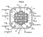
- Figs. 1 to 3 depict a configuration of a light source device according to a first embodiment of the present invention, where Fig. 1 is a sectional view, Fig. 2 is a bottom view, and Fig. 3 is an exploded view.
- Fig. 1 is the sectional view taken along a line 1-1 in Fig. 2 .
- a base 1 is formed from aluminum die-cast, seven stepped holes 1a to 1g in total are formed in the base 1 at a center and on a circumference around this center at equal distances from one another on the circumference.
- Semicircular notches 1h and 1i having different sizes are precisely formed in outer peripheral portions of the base 1. Centers of the notches 1h and 1i are asymmetric about a center of the stepped hole 1d formed at the central portion.
- a first collimator lens 2, a first spacer 3, and a second collimator lens 4 are fitted to each of the seven stepped holes 1a to 1g, and the second collimator lens 4 slightly projects from an upper surface 1j of the base 1.
- a leaf spring 5 is formed into a flat-plate shape by etching a spring stainless steel (SUS301) such that gimbal springlike spring portions are provided at positions corresponding to the seven stepped holes 1a to 1g of the base 1. Notches 5a and 5b are provided at positions corresponding to the notches 1h and 1i of the base 1.
- a restraining plate 6 is formed into a flat-plate shape by stamping a stainless material (SUS304) thicker than the leaf spring 5 such that holes corresponding to the seven stepped holes 1a to 1g of the base 1 and notches 6a and 6b corresponding to the notches 1h and 1i of the base 1 are formed.
- the restraining plate 6 presses the leaf spring 5 so that a portion thereof except the spring portion is not deformed.
- the leaf spring 5 and the restraining plate 6 are fixed without deviation by a plurality of screws 7 such that the notches 5a, 5b, 6a, and 6b match with the notches 1h and 1i of the base 1, and the leaf spring 5 and the restraining plate 6 are pressed against the upper surface 1j of the base 1. Because the notches 1h and 1i are arranged asymmetric around the center of the stepped hole 1d that is arranged at the central portion, front and back surfaces of the leaf spring 5 and the restraining plate 6 are determined uniquely.
- a collimator lens group which includes the first collimator lens 2, the first spacer 3, and the second collimator lens 4, is precisely fixed to the base 1 such that a deviation is not generated even if a vibration or an impact is applied. Because an adhesive is not used, even if it becomes necessary to disassemble the device for removing a foreign matter, the device can be disassembled such that all of the parts can be reused, and the optics such as the first collimator lens 2 and the second collimator lens 4 are not contaminated by out gas of an adhesive.
- a lens barrel 8 is made by cutting aluminum.
- a first condenser lens 9, a second spacer 10, and a second condenser lens 11 are fitted into the lens barrel 8, and they are fixed by a screw ring 12.
- the second spacer 10 and the screw ring 12 are made of brass.
- a recess 12a is provided in a central portion of a side surface of the screw ring 12.
- a setscrew 13 is screwed from a side surface of the lens barrel 8, and a tip end of the setscrew 13 is inserted into the recess 12a. With this arrangement, the recess 12a is fixed to the lens barrel 8 such that it is not loosened.
- a receptacle 14 made of brass is fixed to an upper surface of the lens barrel 8 by screws 15 such that an optical fiber 16 can be attached and detached.
- a condenser lens group formed of the first condenser lens 9, the second spacer 10, and the second condenser lens 11 is precisely fixed to the base 1 such that the group is not deviated even if a vibration or an impact is applied to the group.
- an adhesive is not used, even if it becomes necessary to disassemble the device for removing a foreign matter, the device can be disassembled such that all of parts can be reused without damaging the screw portion of the screw ring 12.
- the optics such as the first condenser lens 9, the second condenser lens 11 and the optical fiber 16 are not contaminated by out gas of an adhesive.
- a spacer 17 is a molded article made of polycarbonate having glass fibers, and the base 1 is fitted into a cylindrical portion of the spacer 17. Projections 17a and 17b corresponding to the notches 1h and 1i of the base 1 are formed inside of the cylindrical portion. A projection 17c corresponding to the notch 8a provided in the lens barrel 8 is provided on outside of the cylindrical portion.
- the base 1 and the lens barrel 8 are fastened to the spacer 17 by four conductive screws 18 so that they are restrained from rotating, and a light source module 24 is formed. Because thermal conductivity of the spacer 17 is sufficiently lower than those of the base 1 and the lens barrel 8, heat is not easily transmitted between the base 1 and the lens barrel 8.
- the base 1 and the lens barrel 8 are fastened to each other by the conductive screws 18, they are electrically conductive.
- LDs 19 Semiconductor lasers (hereinafter, Laser Diodes (LDs)) 19 are light sources that emit blue light having wavelength of 445 nanometers. Relative orientations in rotating directions of optical axes (polarizing directions) of the seven LDs 19 with respect to an LD holder 20 are all the same, and the LDs 19 are press-fitted to the LD holder 20. There are seven LDs 19 and LD holders 20 corresponding to the collimator lens group. In the following explanations, when it is necessary to distinguish a certain one among the LDs 19 from each other, they are described as LD-I to LD-VII. When it is necessary to distinguish a certain one among the LD holders 20 from each other, they are described as LD holders I to VII.
- An upper surface 20a of the LD holder 20 to which the LD 19 is press-fitted is arranged such that the upper surface 20a abuts against a bottom surface 1k of the base 1.
- Optical axes of the LDs 19 and the optical axes of the collimator lens groups are adjusted to appropriate positions on the abutment surfaces, and the LD holder 20 is adhered and fixed to the base 1 by acrylic-based ultraviolet cure adhesives 21a and 21b.
- the lens barrel 8 By fixing the lens barrel 8 made of metal to the base 1 by the conductive screws 18 through the plastic spacer 17, the ground of the LD 19 is electrically connected to the lens barrel 8 through the LD holder 20, the base 1, and the screws 18. Therefore, it is possible to suppress generation of unnecessary radiation when the LD 19 is pulse-driven at high frequencies.
- the lens barrel 8 can be fixed to a later-described Peltier module 34 through the plastic spacer 17 by using a conductive screw.
- Figs. 4-1 and 4-2 are perspective views of a detailed configuration of the LD holder 20.
- the LD holder 20 is of a substantially cylindrical shape, and an outer peripheral surface of the LD holder 20 includes two pairs of notched portions 20b and 20c, as well as 20d and 20e that are symmetric about a center axis of an inner surface hole 201.
- a stepped portion 20g and two pairs of hole portions 20h and 20i as well as 20j and 20k, which are symmetric about the optical axis of the LD 19, are provided in a lower surface 20f of the LD holder 20.
- the lower surface 20f is opposite from the upper surface 20a that abuts against the base 1.
- the hole portions 20h to 20k are provided such that a line connecting centers of the hole portions 20h and 20i and a line connecting centers of the hole portions 20j and 20k intersects with each other at a right angle.
- the inner surface hole 201 that is a cylindrical inner surface of the LD holder 20 is slightly larger in diameter than a press-fit hole 20m into which the LD 19 is inserted.
- Figs. 5 and 6 are enlarged views of a state after the LD holder 20 into which the LD 19 is press-fitted is adhered and fixed to the base 1.
- the LD 19 is a standard CAN package of ⁇ 5.6 millimeters, and includes a notch 19a on a stem and conduction leads 19b.
- a laser beam is emitted from a laser-beam emitting window 19c.
- a light emitting point 19d of the LD 19 is flush with the upper surface 20a of the LD holder 20 so that even if the LD holder 20 is inclined when adjusting its optical axis in position, an amount of positional deviation of the optical axis of the light emitting point 19d in the vertical direction can be suppressed to the minimum.
- the LD holder 20 is designed such that when the LD 19 is press-fitted, a through hole 22 is formed between the LD 19 and the inner surface hole 201 of the LD holder 20 by the notch 19a of the LD 19. That is, in a state that the LDs 19 are press-fitted into the LD holders 20 and are adhered and fixed to the base 1, small chambers 23, which are formed by the stepped holes 1a to 1g of the base 1, the first collimator lenses 2, the LD holders 20, and the LDs 19, are in communication with outside air through the through hole 22.
- the adhesive 21a that fixes the LD holder 20 is applied to four points that are substantially symmetric about the optical axis of the LD 19.
- the adhesive 21a straddle the bottom surface 1k of the base 1 and the notched portions 20b and 20c, which are an outer peripheral side surface of the LD holder 20.
- the adhesive 21b is applied substantially symmetrically about the optical axis of the LD 19 and straddle the bottom surface 1k of the base 1 and the notched portions 20d and 20e, which are the outer peripheral side surface of the LD holder 20. As shown in Fig.
- the LD holders III to VII are arranged such that the stepped portions 20g are oriented to the same direction; however, the LD holder I is arranged in a direction rotated 90° and the LD holder II is arranged in a direction rotated -90°.
- the light source module 24 has the configuration described above.
- the substantially cylindrical LD holder 20 has the notched portions 20b and 20c as well as 20d and 20e that are symmetric about the center axis thereof, and the adhesives 21a and 21b are applied to the notched portions 20b to 20e.
- This configuration can suppress the increase in adhering margins, narrow a distance between the optical axes, and reduce the sizes of the entire device. Because the adhesive is applied to a plurality of locations that are substantially symmetric about the optical axis of the LD 19, even if the adhesive is cured and shrunk or linearly expanded, these phenomena cancel out each other, and a positional deviation is not generated in the LD holder 20. With this configuration, the yield of the light source device can be enhanced.
- Diverging light 25a emitted from the LD 19 is converted into parallel light 25b by the collimator lens group formed of the first collimator lens 2 and the second collimator lens 4. Furthermore, the light 25b is concentrated on an end surface of the optical fiber 16 having a diameter of 400 micrometers by the condenser lens group formed of the first condenser lens 9 and the second condenser lens 11. Incidentally, precision of the parts and precision of assembling position have errors from design center values. A focal point 25c can be deviated from the end surface of the optical fiber 16 and a loss can be generated, and the amount of light entering the optical fiber 16 can be reduced in some cases.
- the focal point 25c can be moved in the direction intersecting with the optical axis at right angles. Therefore, a positional deviation of the light emitting point 19d of the LD 19, positional deviations of the optical axes of the first collimator lenses 2a to 2g and the second collimator lenses 4a to 4g, inclinations of the first condenser lens 9 and the second condenser lens 11, and a positional deviation of the receptacle 14 can be absorbed by adjusting the position of the LD 19 in the direction intersecting with the optical axis at right angles.
- the focal point 25c can be aligned with the end surface of the optical fiber 16.
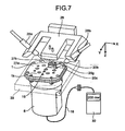
- a movable block 26 is driven in X, Y, and Z directions by an electric inching stage (not shown).
- Two pointed adjusting pins 27a and 27b capable of moving in the Z direction, and two UV fibers 28a and 28b for applying ultraviolet light (hereinafter, UV light) for curing the adhesive are fixed.
- the two adjusting pins 27a and 27b are elastically supported independent from each other to push the LD holder 20 against the bottom surface 1k of the base 1 (in a +Z direction in Figs. 7 and 9 ).
- the pushing force of each of the adjusting pins 27a and 27b is set to about 0.05 Newton (5-gram weight) so that the LD holder 20 does not float from the bottom surface 1k of the base 1, but smoothly moves on the abutment surface.
- the UV fibers 28a and 28b are arranged such that a pair of the notched portions 20b and 20c of the LD holder 20 and the bottom surface 1k of the base 1 near the notched portions are irradiated with light at those spots.
- a socket (not shown) for supplying current is mounted on the LD 19 so that the LD 19 can emit light at a predetermined current.
- the light source module 24 before the LD 19 and the LD holder 20 are fixed thereto is mounted on a fixing block 29 with no backlash.
- the fixing block 29 is shown with broken lines in Figs. 7 and 9 and members located behind the fixing block 29 are shown through the fixing block 29.
- the optical fiber 16 is mounted on the receptacle 14, and a laser beam emitted from the end surface of the opposite end surface of the optical fiber 16 is received by an optical power meter 30.
- the LD holder 20 into which the LD 19 is press-fitted is set, and the adjusting pins 27a and 27b are inserted into a pair of the hole portions 20h and 20i.
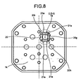
- the stepped portion 20g of the LD holder 20 is set such that it is oriented rightward (the +X direction) in Fig. 8 .
- current of a predetermined current value is made to flow through the LD-I, the movable block 26 is made to move in the X and Y directions such that laser power emitted from the optical fiber 16 becomes maximum, a user checks that the laser power becomes greater than a standard power that was previously obtained by calculation.
- the adhesive 21a is applied to the four locations about the optical axis of the LD 19 so as to straddle the bottom surface 1k of the base 1 and the notched portions 20b and 20c of the outer peripheral surface of the LD holder 20. Then, the adhesive 21a is irradiated with UV light from the UV fibers 28a and 28b and the adhesive 21a is cured. There is nothing that cuts off UV light emitted to the adhesive 21a, and the adhesive 21a can be reliably irradiated with UV light and cured. Because the adhesive 21a is applied to the locations symmetric about the LD holder 20, a deviation of the LD holder 20 is not easily generated when the adhesive is cured and shrunk or linearly expanded.
- the LD holder 20, into which the LD 19 is press-fitted is set on the left side of the LD-I that is adhered and fixed as shown in Fig. 8 such that the stepped portion 20g is oriented leftward (the -X direction).
- LD-II is adjusted and fixed in the same manner as the LD-I.
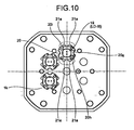
- the LD holder 20, into which the LD 19 is press-fitted is set such that the stepped portion 20g is oriented rightward (the +X direction) in Fig. 10 in a state that the fixing block 29 is rotated 90° in a counterclockwise direction.
- the adjusting pins 27a and 27b are inserted into a pair of the hole portions 20h and 20i, and the LD-III is adjusted and fixed in the same manner as the LD-I.
- the LD-IV to LD-VII are adjusted and fixed in the same manner.
- the fixing block 29 is rotated 90° in the counterclockwise direction when the LD-III to LD-VII are adjusted and fixed; however, they can be also adjusted and fixed by inserting the adjusting pins 27a and 27b into a pair of the hole portions 20j and 20k without rotating the fixing block.
- the light source module 24 is removed from an adjusting device.
- the adhesive 21b which is the same kind as the adhesive 21a, is applied to two locations of each of the seven LD holders 20 so as to straddle the bottom surface 1k of the base 1 and the notched portions 20d and 20e that are outer peripheral surface of the LD holder 20 as shown in Fig. 11 .
- the seven LD holders 20 are collectively irradiated with UV light and adhesive is cured.
- the adhesive 21b is additionally applied to the locations of the LD holder 20 symmetrically and is cured, the positional deviation of the LD holder 20 is not caused by curing and shrinking of the adhesive 21b and the adhering strength of the LD holder 20 can be enhanced. Because the adhesives 21a and 21b are arranged symmetrically on the LD holder 20, to which the LD 19 is fixed, near the abutment surface between the base 1 and the LD holder 20, they are fixed such that a deviation of the LD holder 20 caused by linear expansion of the adhesives 21a and 21b, the positional deviation of the optical axis of the LD 19, and inclination of the optical axis are not generated almost at all.
- the stepped portions 20g of the LD-III to LD-VII of the LD holders 20 are arranged such that they are oriented in the same direction as shown in Fig. 2 ; on the contrary, the LD-I is arranged in the orientation rotated 90° and the LD-II is arranged in the orientation rotated 90° in the opposite direction.
- the polarizing direction of the LD 19 is not constant, a polarizing direction of a laser beam that enters the optical fiber 16 is mixed, and thus color unevenness of a picture when an image is displayed can be suppressed (uniformity can be improved).
- the LDs 19 are press-fitted into the LD holders 20 such that the polarizing directions thereof are set the same, and the LD holders 20 are fixed to the base 1 such that orientations of some of the LD holders 20 are changed. Therefore, the polarizing directions of the LDs 19 are mixed, and the color unevenness of a picture can be suppressed.
- the adjusting operations can be performed at one location. Also, variation in part size and variation in optical characteristics can be absorbed, and the centering operation to the optimal position can be performed. That is, by relatively moving the LD holder 20, to which the LD 19 is fixed, within the abutment surface with respect to the base 1 to which the optics (the first collimator lens 2, the second collimator lens 4, the first condenser lens 9, and the second condenser lens 11) is fixed, the position of the optical axis of the LD 19 can be adjusted with one positioning operation.
- the abutment surface of the base 1 and the side surface of the LD holder 20 are adhered to each other, they can be reliably fixed to each other even if the LD holder 20 and the base 1 do not have UV-permeability, and durability is enhanced.
- the adjusting pins 27a and 27b of the adjusting device are pressed against the position-adjusting recesses (the hole portions 20h to 20k) provided in the lower surface 20f of the LD holder 20 and the position adjustment is performed. Therefore, the position adjustment in the order of micron can be easily performed, a shadow of an adjusting jig does not appear on the adhesive, and the adhesive can be reliably irradiated with UV.
- the LD holder 20 is adhered and cured with high reliability such that the LD holder 20 is not deviated when it is adhered and after it was adhered.
- the adhesives 21a and 21b generate acrylate-based monomer (monomer of acrylic ester) as out gas when they are cured, the out gas enters the small chamber 23 through a gap of several microns due to surface roughness formed on the abutment surface of between the base 1 and the LD holder 20, and the out gas exists in a form of gas. If the LD 19 lights up in this state, out gases are superposed on each other by photon energy, and the out gasses become fine particles and adhere to peripheries.
- This fouling causes a problem that it adheres also to surfaces of the laser-beam emitting window 19c of the LD 19 and the first collimator lens 2, at which photon energy density is particularly high.
- the permeability of the laser beam emitted from the LD 19 is lowered over time.
- the base 1 on the side of the bottom surface 1k is intimately mounted on a decompressor 31, and out gases dispersed in the small chambers 23 at seven locations are collectively sucked and removed from the through hole 22. As described above, the out gas generated when the adhesive is cured is removed from an optical path, and contamination generated by interaction between the LD 19 and the photon energy is suppressed.
- an acrylic-based UV cure adhesive discharges gas even by heat. Therefore, out gas components are exhausted from the adhesives 21a and 21b by subjecting the light source module 24 to thermal processing. For example, if the acrylic-based UV cure adhesive is heated at 65°C for 9 hours, remaining out gas amount can be reduced by 10% or less as compared with UV cure adhesive. At this time, because out gas generated from the adhesives 21a and 21b enters the small chamber 23 through a gap between the abutment surfaces of the base 1 and the LD holder 20. For this reason, the base 1 on the side of the bottom surface 1k is intimately mounted on the decompressor 31 after the thermal processing as shown in Fig.
- the light source module 24 is adjusted and assembled as described above.
- a UV cure adhesive is used as the adhesive 21 for fixing the LD holder 20 to the base 1, thermal processing is performed after the UV curing operation to generate out gas from the adhesive 21, out gas in the small chambers 23, each of which is formed by the stepped holes 1a to 1g of the base 1, the first collimator lens 2, the LD holder 20, and the LD 19, is sucked and exhausted from the through hole 22.
- thermal processing is performed after the UV curing operation to generate out gas from the adhesive 21, out gas in the small chambers 23, each of which is formed by the stepped holes 1a to 1g of the base 1, the first collimator lens 2, the LD holder 20, and the LD 19, is sucked and exhausted from the through hole 22.
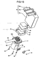
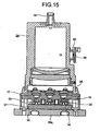
- Figs. 13 to 15 depict a configuration of the light source device in its entirety, in which a flexible printed board (FPC) 32 as a feeding unit, a radiation unit 36 as a cooling unit, and an optical sensor are mounted on the light source module 24.
- Fig. 13 is an exploded view
- Fig. 14 is a perspective view after assembling
- Fig. 15 is a sectional view taken along a line 15-15 in Fig. 14 .
- the FPC 32 for supplying current to the LD 19 is made of polyimide, which has excellent light resistance and heat resistance.
- the FPC 32 passes through the stepped portion 20g of the LD holder 20 and is soldered to the conduction leads 19b that are an anode and a cathode of the LD 19.
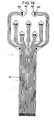
- the FPC 32 includes substantially circular LD-mounting portions 32a on which the LD 19 is mounted.
- Each of the LD-mounting portions 32a includes a soldering land 32b having holes, and a projection 32c formed on a tip end of the LD-mounting portion 32a. Because the projection 32c comes into elastic contact with an inner surface hole 201 of the LD holder 20, the conduction leads 19b, and the holes of the soldering land 32b are pushed against one side (see Figs. 17 and 18 ).
- the LD-mounting portion 32a is fixed such that it is not pulled from the LD holder 20 and does not rattle even before the LD-mounting portion 32a is soldered to the LD 19.
- the LD-mounting portions 32a of the FPC 32 are stably fixed independently, the LDs 19 can be easily and reliably soldered even when there are a plurality of the LDs 19. Because the through hole 22 is closed with the projection 32c of the FPC 32, flux at the time of the soldering operation does not scatter, its fumes do not enter the small chamber 23 easily, and thus it is possible to prevent unwanted material from adhering to surfaces of the laser-beam emitting window 19c of the LD 19 and the first collimator lens 2.
- a thermal-conductive sheet 33 is made of a silicon-based elastic material having thickness of 0.5 millimeter.
- the Peltier module 34 includes a Peltier device, and a surface temperature thereof can be controlled by flowing a current through the Peltier device.
- the thermal-conductive sheet 35 has the same configuration as that of the thermal-conductive sheet 33.
- the radiation unit 36 includes a heat block 36a, a heat pipe 36b, and a fin 36c.
- a Peltier cover 37 is a molded article of polycarbonate having glass fibers like the spacer 17. The Peltier cover 37 is designed such that it can be positioned with respect to the base 1, the Peltier module 34 and the heat block 36a. Four fixing screws 38 are uniformly fastened to the heat block 36a through the Peltier cover 37 from the side of the base 1.
- the thermal-conductive sheet 33 and the thermal-conductive sheet 35 are elastically deformed, and the LD holder 20, the thermal-conductive sheet 33, the Peltier module 34, the thermal-conductive sheet 35, and the heat block 36a are intimately fixed.
- the Peltier cover 37 is positioned to a height where the Peltier cover 37 comes into contact with the spacer 17 and the heat block 36a that are fixed to the base 1 in a state that the fixing screws 38 are fastened, and the base 1 and the heat block 36a cannot approach each other more than this. Therefore, it is possible to avoid a case where an excessive force is applied to the Peltier module 34 due to excessive fastening of the fixing screws 38, or a vibration or an impact from outside, and the Peltier module 34 is damaged.
- the heat block 36a is fixed to the base 1 by the conductive fixing screws 38 through the plastic Peltier cover 37. With this configuration, a thermal capacity of a portion thereof cooled by the Peltier module 34 is reduced, and the LD 19 can be efficiently cooled. That is, the energy required for cooling the LD 19 can be reduced. Also, the lifetime of the LD 19 can be increased.
- An optical sensor is fixed to an optical sensor module 39.
- the optical sensor module 39 is fixed to the lens barrel 8 by a screw 41 through a sensor holder 40 so that a laser beam leaking from a hole 8b formed in a side surface of the lens barrel 8 can be detected.
- a position and a diameter of the hole 8b are designed such that the optical sensor is not saturated.
- the operation of the light source device is described.
- a predetermined current flows through the FPC 32 in a state that the LDs 19 are connected to the control board in series.
- the LD 19 generates heat
- the LD 19 is cooled to a predetermined temperature by the Peltier module 34 through the LD holder 20 and the thermal-conductive sheet 33 based on temperature information of a thermistor (not shown) fixed to the base 1.
- a thermistor (not shown) fixed to the base 1. Because the lens barrel 8 is thermally separated from the base 1 by the spacer 17, a thermal capacity in a range where the temperature is adjusted does not become large more than necessary, and it is possible to efficiently adjust the temperature.
- the optical sensor module 39 can detect a laser beam that reflects on an inner surface of the lens barrel 8 when the LD 19 emits light and that leaks from the hole 8b.
- the optical sensor module 39 compares the laser beam with laser power emitted from the optical fiber 16, thereby monitoring whether there is abnormality such as bending or deterioration of the optical fiber 16.
- the optical sensor module 39 is used for emergency stopping processing for interrupting the current that is supplied to the LD 19.
- the LD 19 is driven at necessary temperature and current, and is operated while monitoring that power is normally emitted from the optical fiber 16.
- the conduction lead 19b of the LD 19 and the FPC 32 are soldered to each other in the inner surface hole 201 of the LD holder 20, and the Peltier module 34 is intimately arranged on the lower surface 20f of the LD holder 20 through the thermal-conductive sheet 33.
- the FPC 32 can be connected using a small space, and LD 19 can be cooled efficiently and easily without sealing the LD 19 air-tightly.
- the through hole that is in communication with outside air is provided in the LD holder 20 to which the LD 19 is fixed, the position of the LD holder is adjusted, and it is adhered and fixed.
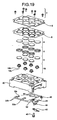
- Figs. 19 to 21 depict a configuration of relevant parts of a light source device according to a second embodiment the present invention.
- Fig. 19 depicts an exploded view
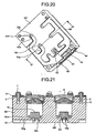
- Fig. 20 depicts an assembly diagram
- Fig. 21 depicts a sectional view taken along a line 21-21 in Fig. 20 .
- Parts shown in the drawings are components corresponding to the base 1, the collimator lens group, the leaf spring 5, the restraining plate 6, the screws 7, the LDs 19, and the LD holders 20 according to the first embodiment.
- the members identical to those of the first embodiment are denoted by like reference numerals.
- six LDs 19 are press-fitted and fixed into press-fit holes 50m of single base holder 50 from the side of the conduction leads 19b.
- the LDs 19 are arranged three each in a state in which rotating directions of optical axes of the LDs 19 are different from each other through 90° so that polarizing directions of the LDs 19 are not directed to the same orientation.
- Six first collimator lenses 2, six first spacers 3, and six second collimator lenses 4 are fitted into the base holder 50 corresponding to the six LDs 19.
- the collimator lens groups are precisely fixed to the base holder 50 such that the groups are not deviated even if a vibration or an impact is applied. This is made by fixing the one leaf spring 5 and the one restraining plate 6 to each other by the screws 7 without a deviation.
- Inner surface holes 501 which are arranged corresponding to the six LDs 19 so as to accommodate the conduction leads 19b, and a groove 50g in which the FPC 32 passes are formed in a back surface 50f of the base holder 50.
- the FPC 32 and tip ends of the conduction leads 19b are configured not to protrude from the back surface 50f of the base holder 50.
- the substantially circular LD-mounting portion 32a of the FPC 32, which is attached to the LD 19, has the soldering lands 32b each having a hole and the projection 32c at a tip end thereof.
- the projection 32c comes into elastic contact with the inner surface hole 501 of the base holder 50, the conduction leads 19b and the holes of the soldering lands 32b are pressed against one side. Then, the LD-mounting portion 32a is fixed such that it is not pulled out from the base holder 50 and it does not rattle even before the LD-mounting portion 32a is soldered to the LD 19.
- the LD-mounting portions 32a of the FPC 32 are stably fixed, it is possible to achieve soldering of the LDs 19 with better operability and higher reliability.
- a thermistor 42 that measures a temperature of the base holder 50 is fixed to a recess formed in the back surface 50f of the base holder 50 by a screw 43 such that the thermistor 42 does not protrude from the back surface 50f. Furthermore, the thermistor 42 is soldered to the FPC 32.
- the LDs 19 and a connector 44 that connects the thermistor 42 and an external board with each other are soldered to an end of the FPC 32, and they are positioned and fixed to a side surface of the base holder 50 by screws 45.
- Fig. 23 depicts a sectional view of the light source device after assembling a condenser lens and a cooling unit 46.
- the cooling unit 46 that can perform temperature adjustment by using a tiller or a Peltier module is closely arranged on the back surface 50f of the base holder 50 through a thermal-conductive sheet 33 by screws, thereby cooling the LDs 19.
- the lens barrel 8 to which the condenser lens 9 is fixed is fastened to the cooling unit 46 by conductive screws 38 through the spacer 17 that is a molded article made of polycarbonate having glass fibers.
- the spacer 17 has sufficiently lower thermal conductivity than those of the cooling unit 46 and the lens barrel 8.
- the ground of the LD 19 is electrically connected to the lens barrel 8 through the base holder 50 and the fixing screws 38 by fixing the metal lens barrel 8 to the cooling unit 46 by the conductive fixing screws 38 through the plastic spacer 17.
- the lens barrel 8 can be fixed to the base holder 50 through the plastic spacer 17 using a conductive screw.
- the FPC 32 and the conduction leads 19b of the LD 19 are soldered to each other in the inner surface hole 501 of the base holder 50, the FPC 32 can be connected with a small space. Also, because the cooling unit 46 is closely arranged on the back surface 50f of the base holder 50, the LD 19 can be efficiently cooled easily without air-tightly sealing it.
- laser beams are concentrated on the end of the optical fiber having the diameter of 400 micrometers.
- positions of the optical axis of the LD and the optical axis of the collimator lens are adjusted.
- the second embodiment when beams are concentrated on a rod 56 having an end of a large area, it is possible to assemble the LD and the collimator lens with mechanical precision. That is, the optical axes adjustment is not necessarily required. Even with this configuration, it is possible to realize a light source device that can efficiently cool the semiconductor laser with excellent assembling operability.
- the present invention it is possible to increase the lifetime of a light source device while suppressing deterioration in light emitting efficiency of a semiconductor laser device due to heat.
Landscapes
- Physics & Mathematics (AREA)
- General Physics & Mathematics (AREA)
- Optics & Photonics (AREA)
- Condensed Matter Physics & Semiconductors (AREA)
- Electromagnetism (AREA)
- Semiconductor Lasers (AREA)
- Optical Couplings Of Light Guides (AREA)
- Projection Apparatus (AREA)
Description
- The present invention relates to a light source device used for a picture display device or the like, and more particularly to a light source device that synthesizes laser beams emitted from a plurality of semiconductor laser devices and concentrates the beams into an optical fiber in order to obtain a predetermined light output.
- A conventional light source device, which synthesizes laser beams emitted from a plurality of semiconductor laser devices and concentrates the beams into an optical fiber, in order to obtain a predetermined light output, is configured to include: a plurality of chip-like semiconductor lasers arranged and fixed on a heat block; collimator lens arrays provided corresponding to the semiconductor lasers; a condenser lens that concentrates collimator light flux generated by the collimator lens arrays into one optical fiber; and a box-like package that air-tightly seals these multiplexing optical systems.
- According to the light source device of this kind, to concentrate laser beams emitted from the semiconductor laser devices into an optical fiber, the semiconductor laser devices, the collimator lens arrays, the condenser lens, and the optical fiber must be fixed with a predetermined positional precision in a state that inclinations of these parts precisely match with each other. To fix these parts in this manner, there is proposed a structure in which inclinations of precisely formed parts are measured by a laser automatic collimator and in this state, these parts are positioned precisely by a mechanical hand and are adhered and fixed (see, for example, Japanese Patent Application Laid-open No.
2006-284851 Page 7 andFig. 1 )). - When a semiconductor laser device having an emission wavelength in a range of 350 to 450 nanometers is used, organic gas (out gas) components of e.g., an adhesive for fixing multiplexing optical systems are deposited on a light emitting unit and an optical member, and this deteriorates laser characteristics. To solve this problem, there is proposed a light source device in which the concentration of organic gas in a package is limited to less than 1000 parts per million (ppm), and inert gas having an oxygen concentration in a range of 1 to 100 ppm is enclosed into the package (see, for example, Japanese Patent No.
4115732 Page 5 andFig. 2 )). - Document
US 6,343,092 B1 discloses a light source comprising semiconductor laser modules and a flat base having through bores for accomodating the laser modules. - However, the conventional light source device has a problem in that, due to the above configuration, a structure for taking wires for driving the semiconductor laser out of the hermetic package becomes complicated.
- The semiconductor laser device generates a large quantity of heat by emitting light, and accordingly has characteristics such that its light emitting efficiency is deteriorated by the heat and thus its lifetime is reduced, and its wavelength is shifted. Therefore, it is important to control heat radiation and the temperature thereof. However, the semiconductor laser device has a problem in that it cannot efficiently release the heat to outside from a fixed heat block to which the semiconductor laser device is fixed. Because the condenser lens and the semiconductor laser device are arranged on the same base plate, the thermal capacity of a portion whose temperature is to be controlled is large, and the cooling operation cannot be efficiently performed.
- The present invention has been achieved in view of the above problems, and an object of the present invention is to provide a light source device capable of efficiently cooling a semiconductor laser device without air-tightly sealing the device.
- A light source device according to an aspect of the present invention, as defined in
claim 1, having a plurality of laser modules, in each of which a semiconductor laser is arranged on one side of a stem and electricity-receiving terminals, which receive electricity for driving the semiconductor laser, are arranged on the other side of the stem, and configured to concentrate laser beams emitted from the laser modules and emit the concentrated laser beams, includes: a module fixing body having a plurality of mounting holes into which the laser modules are fitted and accommodated, respectively; an electricity-supplying member having an end provided with electricity-supplying terminals, which are connected to the electricity-receiving terminals of the laser module accommodated in the mounting hole; and a cooling member that cools each of the laser modules, wherein a groove in which the electricity-supplying member is accommodated is formed in a surface of the module fixing body, and the cooling member is closely arranged on the surface of the module fixing body. - The above and other objects, features, advantages and technical and industrial significance of this invention will be better understood by reading the following detailed description of presently preferred embodiments of the invention, when considered in connection with the accompanying drawings.
-
-
Fig. 1 depicts a sectional view of a configuration of a light source device according to a first embodiment of the present invention; -
Fig. 2 depicts a bottom view of a configuration of the light source device according to the first embodiment; -
Fig. 3 depicts an exploded view of a configuration of the light source device according to the first embodiment; -
Figs. 4-1 and 4-2 depict perspective views of a detailed configuration of an LD holder according to the first embodiment; -
Fig. 5 depicts an enlarged view of a state after the LD holder into which an LD according to the first embodiment is press-fitted is adhered and fixed to a base; -
Fig. 6 depicts another enlarged view of a state after the LD holder into which the LD according to the first embodiment is press-fitted is adhered and fixed to a base; -
Fig. 7 depicts a perspective view explaining an adjusting and fixing method of an LD-I according to the first embodiment; -
Fig. 8 depicts a bottom view explaining the adjusting and fixing method of the LD-I according to the first embodiment; -
Fig. 9 depicts a perspective view explaining an adjusting and fixing method of an LD-III according to the first embodiment; -
Fig. 10 depicts a bottom view explaining the adjusting and fixing method of the LD-III according to the first embodiment; -
Fig. 11 depicts a bottom view explaining a method of additionally applying and curing an adhesive according to the first embodiment; -
Fig. 12 depicts a schematic diagram explaining a method of sucking out gas according to the first embodiment; -
Fig. 13 depicts an exploded view of a configuration of the entire light source device according to the first embodiment; -
Fig. 14 depicts a perspective view of a configuration of the light source device according to the first embodiment in its entirety after assembling; -
Fig. 15 depicts a sectional view of a configuration of the entire light source device according to the first embodiment; -
Fig. 16 depicts a configuration of a flexible printed board according to the first embodiment; -
Fig. 17 depicts a sectional view explaining a soldering method of the flexible printed board according to the first embodiment; -
Fig. 18 depicts a bottom view explaining the soldering method of the flexible printed board according to the first embodiment; -
Fig. 19 depicts an exploded view of a configuration of relevant parts of a light source device according to a second embodiment the present invention; -
Fig. 20 depicts an assembly diagram of a configuration of relevant parts of the light source device according to the second embodiment; -
Fig. 21 depicts a sectional view of a configuration of relevant parts of the light source device according to the second embodiment; -
Fig. 22 depicts a bottom view of a soldering method of a flexible printed board according to the second embodiment; and -
Fig. 23 depicts a sectional view of a configuration of the entire light source device according to the second embodiment. - Exemplary embodiments of a light source device according to the present invention will be explained below in detail with reference to the accompanying drawings. The present invention is not limited to the embodiments.
-
Figs. 1 to 3 depict a configuration of a light source device according to a first embodiment of the present invention, whereFig. 1 is a sectional view,Fig. 2 is a bottom view, andFig. 3 is an exploded view.Fig. 1 is the sectional view taken along a line 1-1 inFig. 2 . - A
base 1 is formed from aluminum die-cast, sevenstepped holes 1a to 1g in total are formed in thebase 1 at a center and on a circumference around this center at equal distances from one another on the circumference.Semicircular notches base 1. Centers of thenotches stepped hole 1d formed at the central portion. Afirst collimator lens 2, afirst spacer 3, and asecond collimator lens 4 are fitted to each of the seven steppedholes 1a to 1g, and thesecond collimator lens 4 slightly projects from an upper surface 1j of thebase 1. Aleaf spring 5 is formed into a flat-plate shape by etching a spring stainless steel (SUS301) such that gimbal springlike spring portions are provided at positions corresponding to the seven steppedholes 1a to 1g of thebase 1.Notches notches base 1. Arestraining plate 6 is formed into a flat-plate shape by stamping a stainless material (SUS304) thicker than theleaf spring 5 such that holes corresponding to the sevenstepped holes 1a to 1g of thebase 1 andnotches notches base 1 are formed. Therestraining plate 6 presses theleaf spring 5 so that a portion thereof except the spring portion is not deformed. Theleaf spring 5 and therestraining plate 6 are fixed without deviation by a plurality ofscrews 7 such that thenotches notches base 1, and theleaf spring 5 and therestraining plate 6 are pressed against the upper surface 1j of thebase 1. Because thenotches stepped hole 1d that is arranged at the central portion, front and back surfaces of theleaf spring 5 and therestraining plate 6 are determined uniquely. Also, theleaf spring 5 and therestraining plate 6 do not float or deviate from each other due to a burr or a flatness of the part. With the above configuration, a collimator lens group, which includes thefirst collimator lens 2, thefirst spacer 3, and thesecond collimator lens 4, is precisely fixed to thebase 1 such that a deviation is not generated even if a vibration or an impact is applied. Because an adhesive is not used, even if it becomes necessary to disassemble the device for removing a foreign matter, the device can be disassembled such that all of the parts can be reused, and the optics such as thefirst collimator lens 2 and thesecond collimator lens 4 are not contaminated by out gas of an adhesive. - A
lens barrel 8 is made by cutting aluminum. Afirst condenser lens 9, asecond spacer 10, and asecond condenser lens 11 are fitted into thelens barrel 8, and they are fixed by ascrew ring 12. Thesecond spacer 10 and thescrew ring 12 are made of brass. Arecess 12a is provided in a central portion of a side surface of thescrew ring 12. Asetscrew 13 is screwed from a side surface of thelens barrel 8, and a tip end of thesetscrew 13 is inserted into therecess 12a. With this arrangement, therecess 12a is fixed to thelens barrel 8 such that it is not loosened. Areceptacle 14 made of brass is fixed to an upper surface of thelens barrel 8 byscrews 15 such that anoptical fiber 16 can be attached and detached. With this configuration, a condenser lens group formed of thefirst condenser lens 9, thesecond spacer 10, and thesecond condenser lens 11 is precisely fixed to thebase 1 such that the group is not deviated even if a vibration or an impact is applied to the group. Because an adhesive is not used, even if it becomes necessary to disassemble the device for removing a foreign matter, the device can be disassembled such that all of parts can be reused without damaging the screw portion of thescrew ring 12. Also, the optics such as thefirst condenser lens 9, thesecond condenser lens 11 and theoptical fiber 16 are not contaminated by out gas of an adhesive. - A
spacer 17 is a molded article made of polycarbonate having glass fibers, and thebase 1 is fitted into a cylindrical portion of thespacer 17.Projections notches base 1 are formed inside of the cylindrical portion. Aprojection 17c corresponding to thenotch 8a provided in thelens barrel 8 is provided on outside of the cylindrical portion. In a state that thebase 1 and thelens barrel 8 are positioned precisely, they are fastened to thespacer 17 by fourconductive screws 18 so that they are restrained from rotating, and alight source module 24 is formed. Because thermal conductivity of thespacer 17 is sufficiently lower than those of thebase 1 and thelens barrel 8, heat is not easily transmitted between thebase 1 and thelens barrel 8. In addition, because thebase 1 and thelens barrel 8 are fastened to each other by theconductive screws 18, they are electrically conductive. - Semiconductor lasers (hereinafter, Laser Diodes (LDs)) 19 are light sources that emit blue light having wavelength of 445 nanometers. Relative orientations in rotating directions of optical axes (polarizing directions) of the seven
LDs 19 with respect to anLD holder 20 are all the same, and theLDs 19 are press-fitted to theLD holder 20. There are sevenLDs 19 andLD holders 20 corresponding to the collimator lens group. In the following explanations, when it is necessary to distinguish a certain one among theLDs 19 from each other, they are described as LD-I to LD-VII. When it is necessary to distinguish a certain one among theLD holders 20 from each other, they are described as LD holders I to VII. Anupper surface 20a of theLD holder 20 to which theLD 19 is press-fitted is arranged such that theupper surface 20a abuts against abottom surface 1k of thebase 1. Optical axes of theLDs 19 and the optical axes of the collimator lens groups are adjusted to appropriate positions on the abutment surfaces, and theLD holder 20 is adhered and fixed to thebase 1 by acrylic-basedultraviolet cure adhesives - By fixing the
lens barrel 8 made of metal to thebase 1 by theconductive screws 18 through theplastic spacer 17, the ground of theLD 19 is electrically connected to thelens barrel 8 through theLD holder 20, thebase 1, and thescrews 18. Therefore, it is possible to suppress generation of unnecessary radiation when theLD 19 is pulse-driven at high frequencies. Thelens barrel 8 can be fixed to a later-describedPeltier module 34 through theplastic spacer 17 by using a conductive screw. -
Figs. 4-1 and 4-2 are perspective views of a detailed configuration of theLD holder 20. TheLD holder 20 is of a substantially cylindrical shape, and an outer peripheral surface of theLD holder 20 includes two pairs of notchedportions inner surface hole 201. A steppedportion 20g and two pairs ofhole portions LD 19, are provided in alower surface 20f of theLD holder 20. Thelower surface 20f is opposite from theupper surface 20a that abuts against thebase 1. Thehole portions 20h to 20k are provided such that a line connecting centers of thehole portions hole portions inner surface hole 201 that is a cylindrical inner surface of theLD holder 20 is slightly larger in diameter than a press-fit hole 20m into which theLD 19 is inserted. -
Figs. 5 and6 are enlarged views of a state after theLD holder 20 into which theLD 19 is press-fitted is adhered and fixed to thebase 1. TheLD 19 is a standard CAN package of φ5.6 millimeters, and includes anotch 19a on a stem and conduction leads 19b. A laser beam is emitted from a laser-beam emitting window 19c. Alight emitting point 19d of theLD 19 is flush with theupper surface 20a of theLD holder 20 so that even if theLD holder 20 is inclined when adjusting its optical axis in position, an amount of positional deviation of the optical axis of thelight emitting point 19d in the vertical direction can be suppressed to the minimum. With this configuration, its centering operability and reliability of a product are enhanced. TheLD holder 20 is designed such that when theLD 19 is press-fitted, a throughhole 22 is formed between theLD 19 and theinner surface hole 201 of theLD holder 20 by thenotch 19a of theLD 19. That is, in a state that theLDs 19 are press-fitted into theLD holders 20 and are adhered and fixed to thebase 1,small chambers 23, which are formed by the steppedholes 1a to 1g of thebase 1, thefirst collimator lenses 2, theLD holders 20, and theLDs 19, are in communication with outside air through the throughhole 22. The adhesive 21a that fixes theLD holder 20 is applied to four points that are substantially symmetric about the optical axis of theLD 19. The adhesive 21a straddle thebottom surface 1k of thebase 1 and the notchedportions LD holder 20. The adhesive 21b is applied substantially symmetrically about the optical axis of theLD 19 and straddle thebottom surface 1k of thebase 1 and the notchedportions LD holder 20. As shown inFig. 2 , the LD holders III to VII are arranged such that the steppedportions 20g are oriented to the same direction; however, the LD holder I is arranged in a direction rotated 90° and the LD holder II is arranged in a direction rotated -90°. Thelight source module 24 has the configuration described above. - The substantially
cylindrical LD holder 20 has the notchedportions adhesives portions 20b to 20e. This configuration can suppress the increase in adhering margins, narrow a distance between the optical axes, and reduce the sizes of the entire device. Because the adhesive is applied to a plurality of locations that are substantially symmetric about the optical axis of theLD 19, even if the adhesive is cured and shrunk or linearly expanded, these phenomena cancel out each other, and a positional deviation is not generated in theLD holder 20. With this configuration, the yield of the light source device can be enhanced. - An operation of the present embodiment is described next. Diverging light 25a emitted from the
LD 19 is converted intoparallel light 25b by the collimator lens group formed of thefirst collimator lens 2 and thesecond collimator lens 4. Furthermore, the light 25b is concentrated on an end surface of theoptical fiber 16 having a diameter of 400 micrometers by the condenser lens group formed of thefirst condenser lens 9 and thesecond condenser lens 11. Incidentally, precision of the parts and precision of assembling position have errors from design center values. Afocal point 25c can be deviated from the end surface of theoptical fiber 16 and a loss can be generated, and the amount of light entering theoptical fiber 16 can be reduced in some cases. In this embodiment, when theLD 19 is moved in a direction intersecting with the optical axis at right angles, the optical axis of theparallel light 25b is inclined, and thefocal point 25c can be moved in the direction intersecting with the optical axis at right angles. Therefore, a positional deviation of thelight emitting point 19d of theLD 19, positional deviations of the optical axes of the first collimator lenses 2a to 2g and the second collimator lenses 4a to 4g, inclinations of thefirst condenser lens 9 and thesecond condenser lens 11, and a positional deviation of thereceptacle 14 can be absorbed by adjusting the position of theLD 19 in the direction intersecting with the optical axis at right angles. Thus, thefocal point 25c can be aligned with the end surface of theoptical fiber 16. - An adjusting and fixing method according to the present embodiment is explained next with reference to
Figs. 7 to 10 . Amovable block 26 is driven in X, Y, and Z directions by an electric inching stage (not shown). Two pointed adjustingpins UV fibers pins LD holder 20 against thebottom surface 1k of the base 1 (in a +Z direction inFigs. 7 and9 ). At this time, the pushing force of each of the adjusting pins 27a and 27b is set to about 0.05 Newton (5-gram weight) so that theLD holder 20 does not float from thebottom surface 1k of thebase 1, but smoothly moves on the abutment surface. TheUV fibers portions LD holder 20 and thebottom surface 1k of thebase 1 near the notched portions are irradiated with light at those spots. A socket (not shown) for supplying current is mounted on theLD 19 so that theLD 19 can emit light at a predetermined current. - The
light source module 24 before theLD 19 and theLD holder 20 are fixed thereto is mounted on a fixingblock 29 with no backlash. To facilitate understanding of the configuration, the fixingblock 29 is shown with broken lines inFigs. 7 and9 and members located behind the fixingblock 29 are shown through the fixingblock 29. Theoptical fiber 16 is mounted on thereceptacle 14, and a laser beam emitted from the end surface of the opposite end surface of theoptical fiber 16 is received by anoptical power meter 30. - When the LD-I is to be adjusted and fixed, as shown in
Figs. 7 and8 , theLD holder 20 into which theLD 19 is press-fitted is set, and the adjusting pins 27a and 27b are inserted into a pair of thehole portions portion 20g of theLD holder 20 is set such that it is oriented rightward (the +X direction) inFig. 8 . In this state, current of a predetermined current value is made to flow through the LD-I, themovable block 26 is made to move in the X and Y directions such that laser power emitted from theoptical fiber 16 becomes maximum, a user checks that the laser power becomes greater than a standard power that was previously obtained by calculation. The adhesive 21a is applied to the four locations about the optical axis of theLD 19 so as to straddle thebottom surface 1k of thebase 1 and the notchedportions LD holder 20. Then, the adhesive 21a is irradiated with UV light from theUV fibers LD holder 20, a deviation of theLD holder 20 is not easily generated when the adhesive is cured and shrunk or linearly expanded. Even if theLD holder 20 is inclined, because the positional deviation of thelight emitting point 19d is not easily generated, a value of theoptical power meter 30 is not varied at the time of adjustment. Thus, the adjusting operability is excellent. Also, because the position of thelight emitting point 19d is not easily changed with respect to the inclination of theLD holder 20, a light source device having higher reliability can be provided. - Next, when the LD-II is to be adjusted and fixed, the
LD holder 20, into which theLD 19 is press-fitted, is set on the left side of the LD-I that is adhered and fixed as shown inFig. 8 such that the steppedportion 20g is oriented leftward (the -X direction). Thus, LD-II is adjusted and fixed in the same manner as the LD-I. - When the LD-III is to be fixed, as shown in
Figs. 9 and10 , theLD holder 20, into which theLD 19 is press-fitted, is set such that the steppedportion 20g is oriented rightward (the +X direction) inFig. 10 in a state that the fixingblock 29 is rotated 90° in a counterclockwise direction. Then, the adjusting pins 27a and 27b are inserted into a pair of thehole portions block 29 is rotated 90° in the counterclockwise direction when the LD-III to LD-VII are adjusted and fixed; however, they can be also adjusted and fixed by inserting the adjusting pins 27a and 27b into a pair of thehole portions - When the adjusting and fixing operations of the LD-I to LD-VII are completed, the
light source module 24 is removed from an adjusting device. The adhesive 21b, which is the same kind as the adhesive 21a, is applied to two locations of each of the sevenLD holders 20 so as to straddle thebottom surface 1k of thebase 1 and the notchedportions LD holder 20 as shown inFig. 11 . The sevenLD holders 20 are collectively irradiated with UV light and adhesive is cured. Because the adhesive 21b is additionally applied to the locations of theLD holder 20 symmetrically and is cured, the positional deviation of theLD holder 20 is not caused by curing and shrinking of the adhesive 21b and the adhering strength of theLD holder 20 can be enhanced. Because theadhesives LD holder 20, to which theLD 19 is fixed, near the abutment surface between thebase 1 and theLD holder 20, they are fixed such that a deviation of theLD holder 20 caused by linear expansion of theadhesives LD 19, and inclination of the optical axis are not generated almost at all. The steppedportions 20g of the LD-III to LD-VII of theLD holders 20 are arranged such that they are oriented in the same direction as shown inFig. 2 ; on the contrary, the LD-I is arranged in the orientation rotated 90° and the LD-II is arranged in the orientation rotated 90° in the opposite direction. With this, the polarizing direction of theLD 19 is not constant, a polarizing direction of a laser beam that enters theoptical fiber 16 is mixed, and thus color unevenness of a picture when an image is displayed can be suppressed (uniformity can be improved). That is, theLDs 19 are press-fitted into theLD holders 20 such that the polarizing directions thereof are set the same, and theLD holders 20 are fixed to thebase 1 such that orientations of some of theLD holders 20 are changed. Therefore, the polarizing directions of theLDs 19 are mixed, and the color unevenness of a picture can be suppressed. - Because the positions of the lens and the optical axis of the
LD 19 are adjusted on the abutment surface between thebase 1 to which thelens barrel 8 is fixed and theLD holder 20 to which theLD 19 is fixed, the adjusting operations can be performed at one location. Also, variation in part size and variation in optical characteristics can be absorbed, and the centering operation to the optimal position can be performed. That is, by relatively moving theLD holder 20, to which theLD 19 is fixed, within the abutment surface with respect to thebase 1 to which the optics (thefirst collimator lens 2, thesecond collimator lens 4, thefirst condenser lens 9, and the second condenser lens 11) is fixed, the position of the optical axis of theLD 19 can be adjusted with one positioning operation. Because the abutment surface of thebase 1 and the side surface of theLD holder 20 are adhered to each other, they can be reliably fixed to each other even if theLD holder 20 and thebase 1 do not have UV-permeability, and durability is enhanced. The adjusting pins 27a and 27b of the adjusting device are pressed against the position-adjusting recesses (thehole portions 20h to 20k) provided in thelower surface 20f of theLD holder 20 and the position adjustment is performed. Therefore, the position adjustment in the order of micron can be easily performed, a shadow of an adjusting jig does not appear on the adhesive, and the adhesive can be reliably irradiated with UV. - The
LD holder 20 is adhered and cured with high reliability such that theLD holder 20 is not deviated when it is adhered and after it was adhered. However, because theadhesives small chamber 23 through a gap of several microns due to surface roughness formed on the abutment surface of between thebase 1 and theLD holder 20, and the out gas exists in a form of gas. If theLD 19 lights up in this state, out gases are superposed on each other by photon energy, and the out gasses become fine particles and adhere to peripheries. This fouling causes a problem that it adheres also to surfaces of the laser-beam emitting window 19c of theLD 19 and thefirst collimator lens 2, at which photon energy density is particularly high. The permeability of the laser beam emitted from theLD 19 is lowered over time. To avoid this problem, in the present embodiment, as shown inFig. 12 , thebase 1 on the side of thebottom surface 1k is intimately mounted on adecompressor 31, and out gases dispersed in thesmall chambers 23 at seven locations are collectively sucked and removed from the throughhole 22. As described above, the out gas generated when the adhesive is cured is removed from an optical path, and contamination generated by interaction between theLD 19 and the photon energy is suppressed. Generally, an acrylic-based UV cure adhesive discharges gas even by heat. Therefore, out gas components are exhausted from theadhesives light source module 24 to thermal processing. For example, if the acrylic-based UV cure adhesive is heated at 65°C for 9 hours, remaining out gas amount can be reduced by 10% or less as compared with UV cure adhesive. At this time, because out gas generated from theadhesives small chamber 23 through a gap between the abutment surfaces of thebase 1 and theLD holder 20. For this reason, thebase 1 on the side of thebottom surface 1k is intimately mounted on thedecompressor 31 after the thermal processing as shown inFig. 12 , so that out gases dispersed in thesmall chambers 23 at the seven locations are collectively sucked and eliminated via the throughhole 22. The out gas is eliminated from the optical path in the manner described above, contamination generated by interaction between theLD 19 and the photon energy is further suppressed, and deterioration in permeability of the laser beam emitted from theLD 19 is prevented. Thelight source module 24 is adjusted and assembled as described above. - A UV cure adhesive is used as the adhesive 21 for fixing the
LD holder 20 to thebase 1, thermal processing is performed after the UV curing operation to generate out gas from the adhesive 21, out gas in thesmall chambers 23, each of which is formed by the steppedholes 1a to 1g of thebase 1, thefirst collimator lens 2, theLD holder 20, and theLD 19, is sucked and exhausted from the throughhole 22. Thus, it is possible to reliably remove the out gas and to prevent out gas from being generated with time. -
Figs. 13 to 15 depict a configuration of the light source device in its entirety, in which a flexible printed board (FPC) 32 as a feeding unit, aradiation unit 36 as a cooling unit, and an optical sensor are mounted on thelight source module 24.Fig. 13 is an exploded view,Fig. 14 is a perspective view after assembling, andFig. 15 is a sectional view taken along a line 15-15 inFig. 14 . TheFPC 32 for supplying current to theLD 19 is made of polyimide, which has excellent light resistance and heat resistance. TheFPC 32 passes through the steppedportion 20g of theLD holder 20 and is soldered to the conduction leads 19b that are an anode and a cathode of theLD 19.Figs. 16 to 18 show details of theFPC 32. As shown inFigs. 16 to 18 , theFPC 32 includes substantially circular LD-mountingportions 32a on which theLD 19 is mounted. Each of the LD-mountingportions 32a includes asoldering land 32b having holes, and aprojection 32c formed on a tip end of the LD-mountingportion 32a. Because theprojection 32c comes into elastic contact with aninner surface hole 201 of theLD holder 20, the conduction leads 19b, and the holes of thesoldering land 32b are pushed against one side (seeFigs. 17 and 18 ). The LD-mountingportion 32a is fixed such that it is not pulled from theLD holder 20 and does not rattle even before the LD-mountingportion 32a is soldered to theLD 19. With this configuration, because the LD-mountingportions 32a of theFPC 32 are stably fixed independently, theLDs 19 can be easily and reliably soldered even when there are a plurality of theLDs 19. Because the throughhole 22 is closed with theprojection 32c of theFPC 32, flux at the time of the soldering operation does not scatter, its fumes do not enter thesmall chamber 23 easily, and thus it is possible to prevent unwanted material from adhering to surfaces of the laser-beam emitting window 19c of theLD 19 and thefirst collimator lens 2. It is also possible to prevent scattered light emitted from theLD 19 from leaking out from the throughhole 22. Therefore, it is possible to avoid a case that a material that can be a cause of contamination is generated from a part that is arranged therearound by leaked scattered light. - A thermal-
conductive sheet 33 is made of a silicon-based elastic material having thickness of 0.5 millimeter. ThePeltier module 34 includes a Peltier device, and a surface temperature thereof can be controlled by flowing a current through the Peltier device. The thermal-conductive sheet 35 has the same configuration as that of the thermal-conductive sheet 33. Theradiation unit 36 includes aheat block 36a, aheat pipe 36b, and afin 36c. APeltier cover 37 is a molded article of polycarbonate having glass fibers like thespacer 17. The Peltier cover 37 is designed such that it can be positioned with respect to thebase 1, thePeltier module 34 and theheat block 36a. Four fixingscrews 38 are uniformly fastened to theheat block 36a through the Peltier cover 37 from the side of thebase 1. With this configuration, the thermal-conductive sheet 33 and the thermal-conductive sheet 35 are elastically deformed, and theLD holder 20, the thermal-conductive sheet 33, thePeltier module 34, the thermal-conductive sheet 35, and theheat block 36a are intimately fixed. The Peltier cover 37 is positioned to a height where thePeltier cover 37 comes into contact with thespacer 17 and theheat block 36a that are fixed to thebase 1 in a state that the fixing screws 38 are fastened, and thebase 1 and theheat block 36a cannot approach each other more than this. Therefore, it is possible to avoid a case where an excessive force is applied to thePeltier module 34 due to excessive fastening of the fixing screws 38, or a vibration or an impact from outside, and thePeltier module 34 is damaged. - The
heat block 36a is fixed to thebase 1 by the conductive fixing screws 38 through theplastic Peltier cover 37. With this configuration, a thermal capacity of a portion thereof cooled by thePeltier module 34 is reduced, and theLD 19 can be efficiently cooled. That is, the energy required for cooling theLD 19 can be reduced. Also, the lifetime of theLD 19 can be increased. - An optical sensor is fixed to an
optical sensor module 39. Theoptical sensor module 39 is fixed to thelens barrel 8 by ascrew 41 through asensor holder 40 so that a laser beam leaking from ahole 8b formed in a side surface of thelens barrel 8 can be detected. A position and a diameter of thehole 8b are designed such that the optical sensor is not saturated. - The operation of the light source device is described. First, to make the
LD 19 emit light, a predetermined current flows through theFPC 32 in a state that theLDs 19 are connected to the control board in series. At this time, because theLD 19 generates heat, theLD 19 is cooled to a predetermined temperature by thePeltier module 34 through theLD holder 20 and the thermal-conductive sheet 33 based on temperature information of a thermistor (not shown) fixed to thebase 1. Because thelens barrel 8 is thermally separated from thebase 1 by thespacer 17, a thermal capacity in a range where the temperature is adjusted does not become large more than necessary, and it is possible to efficiently adjust the temperature. Heat generated on a surface opposite from the thermal-conductive sheet 33 when thePeltier module 34 is driven is transmitted to theheat block 36a through the thermal-conductive sheet 35, and transmitted to thefin 36c through theheat pipe 36b and is radiated in the air. Theoptical sensor module 39 can detect a laser beam that reflects on an inner surface of thelens barrel 8 when theLD 19 emits light and that leaks from thehole 8b. Theoptical sensor module 39 compares the laser beam with laser power emitted from theoptical fiber 16, thereby monitoring whether there is abnormality such as bending or deterioration of theoptical fiber 16. When abnormal condition is detected, theoptical sensor module 39 is used for emergency stopping processing for interrupting the current that is supplied to theLD 19. TheLD 19 is driven at necessary temperature and current, and is operated while monitoring that power is normally emitted from theoptical fiber 16. - According to the light source device of the embodiment, the
conduction lead 19b of theLD 19 and theFPC 32 are soldered to each other in theinner surface hole 201 of theLD holder 20, and thePeltier module 34 is intimately arranged on thelower surface 20f of theLD holder 20 through the thermal-conductive sheet 33. With this configuration, theFPC 32 can be connected using a small space, andLD 19 can be cooled efficiently and easily without sealing theLD 19 air-tightly. - The through hole that is in communication with outside air is provided in the
LD holder 20 to which theLD 19 is fixed, the position of the LD holder is adjusted, and it is adhered and fixed. With this configuration, laser beams are synthesized, light is concentrated into the optical fiber, and the productivity and reliability are high although the device is inexpensive. -
Figs. 19 to 21 depict a configuration of relevant parts of a light source device according to a second embodiment the present invention.Fig. 19 depicts an exploded view,Fig. 20 depicts an assembly diagram, andFig. 21 depicts a sectional view taken along a line 21-21 inFig. 20 . Parts shown in the drawings are components corresponding to thebase 1, the collimator lens group, theleaf spring 5, the restrainingplate 6, thescrews 7, theLDs 19, and theLD holders 20 according to the first embodiment. The members identical to those of the first embodiment are denoted by like reference numerals. In the second embodiment, sixLDs 19 are press-fitted and fixed into press-fit holes 50m ofsingle base holder 50 from the side of the conduction leads 19b. To suppress unevenness and ensure uniformity, theLDs 19 are arranged three each in a state in which rotating directions of optical axes of theLDs 19 are different from each other through 90° so that polarizing directions of theLDs 19 are not directed to the same orientation. Sixfirst collimator lenses 2, sixfirst spacers 3, and sixsecond collimator lenses 4 are fitted into thebase holder 50 corresponding to the sixLDs 19. The collimator lens groups are precisely fixed to thebase holder 50 such that the groups are not deviated even if a vibration or an impact is applied. This is made by fixing the oneleaf spring 5 and the onerestraining plate 6 to each other by thescrews 7 without a deviation. - Inner surface holes 501 which are arranged corresponding to the six
LDs 19 so as to accommodate the conduction leads 19b, and agroove 50g in which theFPC 32 passes are formed in aback surface 50f of thebase holder 50. TheFPC 32 and tip ends of the conduction leads 19b are configured not to protrude from theback surface 50f of thebase holder 50. As shown inFig. 22 , the substantially circular LD-mountingportion 32a of theFPC 32, which is attached to theLD 19, has the soldering lands 32b each having a hole and theprojection 32c at a tip end thereof. As theprojection 32c comes into elastic contact with theinner surface hole 501 of thebase holder 50, the conduction leads 19b and the holes of the soldering lands 32b are pressed against one side. Then, the LD-mountingportion 32a is fixed such that it is not pulled out from thebase holder 50 and it does not rattle even before the LD-mountingportion 32a is soldered to theLD 19. With this configuration, even when there areplural LDs 19 to be soldered, because the LD-mountingportions 32a of theFPC 32 are stably fixed, it is possible to achieve soldering of theLDs 19 with better operability and higher reliability. Athermistor 42 that measures a temperature of thebase holder 50 is fixed to a recess formed in theback surface 50f of thebase holder 50 by ascrew 43 such that thethermistor 42 does not protrude from theback surface 50f. Furthermore, thethermistor 42 is soldered to theFPC 32. TheLDs 19 and aconnector 44 that connects thethermistor 42 and an external board with each other are soldered to an end of theFPC 32, and they are positioned and fixed to a side surface of thebase holder 50 byscrews 45. -
Fig. 23 depicts a sectional view of the light source device after assembling a condenser lens and acooling unit 46. The coolingunit 46 that can perform temperature adjustment by using a tiller or a Peltier module is closely arranged on theback surface 50f of thebase holder 50 through a thermal-conductive sheet 33 by screws, thereby cooling theLDs 19. Thelens barrel 8 to which thecondenser lens 9 is fixed is fastened to thecooling unit 46 byconductive screws 38 through thespacer 17 that is a molded article made of polycarbonate having glass fibers. Thespacer 17 has sufficiently lower thermal conductivity than those of the coolingunit 46 and thelens barrel 8. With this configuration, heat is easily transferred from thebase holder 50 to thecooling unit 46; however, heat is not easily transferred from the lens barrel 8 (in other words, a thermal capacity of a portion that is cooled by the coolingunit 46 is small), and thus theLDs 19 can be efficiently cooled. That is, the energy required for cooling theLDs 19 can be reduced, and the lifetime of theLD 19 can be increased. - The ground of the
LD 19 is electrically connected to thelens barrel 8 through thebase holder 50 and the fixing screws 38 by fixing themetal lens barrel 8 to thecooling unit 46 by the conductive fixing screws 38 through theplastic spacer 17. Thus, it is possible to suppress generation of parasitic emissions when theLD 19 is pulse-driven at high frequencies. Similarly to the first embodiment, thelens barrel 8 can be fixed to thebase holder 50 through theplastic spacer 17 using a conductive screw. - Because the
FPC 32 and the conduction leads 19b of theLD 19 are soldered to each other in theinner surface hole 501 of thebase holder 50, theFPC 32 can be connected with a small space. Also, because thecooling unit 46 is closely arranged on theback surface 50f of thebase holder 50, theLD 19 can be efficiently cooled easily without air-tightly sealing it. - In the first embodiment, laser beams are concentrated on the end of the optical fiber having the diameter of 400 micrometers. Thus, positions of the optical axis of the LD and the optical axis of the collimator lens are adjusted. Meanwhile, as in the second embodiment, when beams are concentrated on a
rod 56 having an end of a large area, it is possible to assemble the LD and the collimator lens with mechanical precision. That is, the optical axes adjustment is not necessarily required. Even with this configuration, it is possible to realize a light source device that can efficiently cool the semiconductor laser with excellent assembling operability. - According to the present invention, it is possible to increase the lifetime of a light source device while suppressing deterioration in light emitting efficiency of a semiconductor laser device due to heat.
- Although the invention has been described with respect to specific embodiments for a complete and clear disclosure, the appended claims are not to be thus limited but are to be construed as embodying all modifications and alternative constructions that may occur to one skilled in the art that fairly fall within the basic teaching herein set forth.
Claims (8)
- A light source device having a plurality of laser modules (19), in each of which a semiconductor laser is arranged on one side of a stem and electricity-receiving terminals (19b), which receive electricity for driving the semiconductor laser, are arranged on the other side of the stem, and configured to concentrate laser beams emitted from the laser modules (19) and emit the concentrated laser beams, the light source device comprising a module fixing body (1, 20; 50) into which the laser modules (19) are fitted and accommodated, respectively; wherein,
the module fixing body (1, 20) comprises a plurality of cylindrical holders (20) having mounting holes (20m, 201), and a plate-like base (1) having a plurality of through holes (1a, 1b, 1c, 1d, 1e, 1f, 1g) through which laser beams from the laser modules (19) fixed to the holders (20) pass, the holders (20) being fixed to the base (1) such that the through holes (1a, 1b, 1c, 1d, 1e, 1f, 1g) and the mounting holes (20m, 20l) are connected to each other,
an electricity-supplying member (32) is provided with electricity-supplying terminals (32b), which are connected to the electricity-receiving terminals (19b) of the laser modules (19) accommodated in respective mounting holes (20m, 20l; 50m, 50l), the electricity-supplying member being a flexible printed board which includes mounting portions (32a) on which the laser modules (19) are mounted; and
a cooling member (34, 36a; 46) is fixed to the base (1) of the module fixing body (1, 20) that cools each of the laser modules (19), wherein each holder (20) includes a cutout portion forming a stepped portion (20g; 50g) provided in a lower surface (20f) thereof, through which the electricity-supplying member (32) passes to be soldered to the electricity-receiving terminals (19b) of the respective laser module (19). - The light source device according to claim 1, wherein
a projection (32c) is formed on the end of the electricity-supplying member (32), and
the end of the electricity-supplying member (32) is fixed to the mounting hole (20m, 20l; 50m, 50l) while deforming the projection (32c) by an inner peripheral surface of the mounting hole (20m, 20l; 50m, 50l). - The light source device according to claim 1 or 2, wherein
the cooling member (34, 36a) comprises:a Peltier module (34) being abutted against the module fixing body (1, 20) on a heat-absorbing side thereof, anda heat block (36a) arranged on a heat-generating side of the Peltier module (34). - The light source device according to claim 1, further comprising:a cylindrical lens holding body (8) that is fixed to the base (1) and holding a condenser lens (9) that collectively concentrates the laser beams emitted from the through holes (1a, 1b, 1c, 1d, 1e, 1f, 1g), anda spacer (17) that is interposed between the base (1) and the lens holding body (8) and having thermal conductivity lower than that of the lens holding body (8).
- The light source device according to claim 1, further comprising:a cylindrical lens holding body (8) that is fixed to the cooling member (34, 36a) and holding a condenser lens (9) that collectively concentrates the laser beams emitted from the through holes (1a, 1b, 1c, 1d, 1e, 1f, 1g), anda spacer (17) that is interposed between the cooling member (34, 36a) and the lens holding body (8) and having thermal conductivity lower than that of the lens holding body (8).
- The light source device according to any one of claims 1 to 3, wherein the module fixing body (50) is integrally formed.
- The light source device according to claim 6, further comprising:a cylindrical lens holding body (8) that is fixed to the cooling member (46) and holding a condenser lens (9) that collectively concentrates the laser beams emitted from the mounting holes (50m, 50l), anda spacer (17) that is interposed between the cooling member (46) and the lens holding body (8) and having thermal conductivity lower than that of the lens holding body (8).
- The light source device according to claim 6, further comprising:a cylindrical lens holding body (8) that is fixed to the module fixing body (50) and holding a condenser lens (9) that collectively concentrates the laser beams emitted from the mounting holes (50m, 501), anda spacer (17) that is interposed between the module fixing body (50) and the lens holding body (8) and having thermal conductivity lower than that of the lens holding body (8).
Applications Claiming Priority (1)
| Application Number | Priority Date | Filing Date | Title |
|---|---|---|---|
| JP2009248214A JP5473535B2 (en) | 2009-10-28 | 2009-10-28 | Light source device |
Publications (3)
| Publication Number | Publication Date |
|---|---|
| EP2317614A2 EP2317614A2 (en) | 2011-05-04 |
| EP2317614A3 EP2317614A3 (en) | 2012-02-29 |
| EP2317614B1 true EP2317614B1 (en) | 2015-04-15 |
Family
ID=42754554
Family Applications (1)
| Application Number | Title | Priority Date | Filing Date |
|---|---|---|---|
| EP10008176.9A Not-in-force EP2317614B1 (en) | 2009-10-28 | 2010-08-05 | Light source device |
Country Status (5)
| Country | Link |
|---|---|
| US (1) | US8724668B2 (en) |
| EP (1) | EP2317614B1 (en) |
| JP (1) | JP5473535B2 (en) |
| CN (1) | CN102052608B (en) |
| CA (1) | CA2716066C (en) |
Families Citing this family (42)
| Publication number | Priority date | Publication date | Assignee | Title |
|---|---|---|---|---|
| JP5473534B2 (en) * | 2009-10-28 | 2014-04-16 | 三菱電機株式会社 | Light source device |
| JP5934914B2 (en) * | 2011-05-13 | 2016-06-15 | パナソニックIpマネジメント株式会社 | Laser array light source unit |
| CN202351450U (en) * | 2011-06-07 | 2012-07-25 | 奥兰若技术有限公司 | Calibrator assembly with external full-glass shell |
| JP5817313B2 (en) * | 2011-08-09 | 2015-11-18 | セイコーエプソン株式会社 | Light source device and projector |
| WO2013023488A1 (en) * | 2011-08-12 | 2013-02-21 | Li Changxing | Led light source |
| JP5846416B2 (en) * | 2011-08-31 | 2016-01-20 | カシオ計算機株式会社 | Light source device and projector |
| JP5950147B2 (en) | 2011-09-20 | 2016-07-13 | カシオ計算機株式会社 | LIGHT SOURCE DEVICE, PROJECTOR, AND LIGHT SOURCE DEVICE MANUFACTURING METHOD |
| JP2013011841A (en) * | 2011-09-28 | 2013-01-17 | Panasonic Corp | Image display device |
| GB2495774A (en) * | 2011-10-21 | 2013-04-24 | Barco Nv | Laser diode grid element comprised of standard laser diodes on a heat exchange plate and PCB |
| WO2014103019A1 (en) * | 2012-12-28 | 2014-07-03 | Necディスプレイソリューションズ株式会社 | Semiconductor element cooling structure and electronic apparatus provided with same |
| JP6423997B2 (en) * | 2013-07-09 | 2018-11-14 | オリンパス株式会社 | Heat treatment apparatus for light source and light source apparatus |
| JP2015022244A (en) * | 2013-07-23 | 2015-02-02 | 株式会社リコー | Solid light source device and image projection device |
| US9628184B2 (en) | 2013-11-05 | 2017-04-18 | Cisco Technology, Inc. | Efficient optical communication device |
| CN104104013A (en) * | 2014-08-07 | 2014-10-15 | 西安精英光电技术有限公司 | Split type semiconductor laser diode energy beam combination device |
| JP6655287B2 (en) * | 2014-12-25 | 2020-02-26 | 古河電気工業株式会社 | Optical unit, optical unit fixing structure, and semiconductor laser module |
| JP6545991B2 (en) * | 2015-03-31 | 2019-07-17 | 株式会社小糸製作所 | Light source module |
| US10761276B2 (en) | 2015-05-15 | 2020-09-01 | Nlight, Inc. | Passively aligned crossed-cylinder objective assembly |
| CN104901147A (en) * | 2015-06-18 | 2015-09-09 | 潍坊华光数码设备有限公司 | UV laser refrigeration mechanism for CTP |
| JP6553966B2 (en) * | 2015-07-14 | 2019-07-31 | 株式会社小糸製作所 | Light source module |
| JP6137265B2 (en) * | 2015-10-01 | 2017-05-31 | セイコーエプソン株式会社 | Light source device and projector |
| JP6431617B2 (en) * | 2015-10-27 | 2018-11-28 | 三菱電機株式会社 | Laser light source module |
| JP6720502B2 (en) * | 2015-10-30 | 2020-07-08 | 株式会社島津製作所 | Laser device manufacturing method |
| CN105552711B (en) * | 2016-01-29 | 2018-10-26 | 中国科学院长春光学精密机械与物理研究所 | The small-volume large-power semiconductor laser to be radiated using heat pipe radiating system |
| EP3417340A1 (en) | 2016-02-16 | 2018-12-26 | NLIGHT, Inc. | Passively aligned single element telescope for improved package brightness |
| JP6922236B2 (en) * | 2016-03-10 | 2021-08-18 | 株式会社リコー | Laser light emitting device, engine spark plug system |
| JP6739067B2 (en) * | 2016-10-25 | 2020-08-12 | パナソニックIpマネジメント株式会社 | Semiconductor laser device |
| CN106443910A (en) * | 2016-11-17 | 2017-02-22 | 武汉电信器件有限公司 | Precise temperature control coupled platform device for photoelectronic device |
| WO2018200587A1 (en) | 2017-04-24 | 2018-11-01 | Nlight, Inc. | Low swap two-phase cooled diode laser package |
| JP7039909B2 (en) * | 2017-09-27 | 2022-03-23 | セイコーエプソン株式会社 | Lighting equipment and projectors |
| JP7032634B2 (en) * | 2017-09-29 | 2022-03-09 | 日亜化学工業株式会社 | Optical engine and projector |
| US10833482B2 (en) | 2018-02-06 | 2020-11-10 | Nlight, Inc. | Diode laser apparatus with FAC lens out-of-plane beam steering |
| US10673203B2 (en) * | 2018-03-09 | 2020-06-02 | North Inc. | Alignment methods for laser diodes |
| JP7142227B2 (en) * | 2018-05-24 | 2022-09-27 | パナソニックIpマネジメント株式会社 | Exchangeable Laser Cavity with Angular Adjustment |
| CN109084189B (en) * | 2018-06-29 | 2020-06-26 | 北京工业大学 | Remote laser illumination optical system |
| US10746944B2 (en) * | 2018-08-24 | 2020-08-18 | Shimadzu Corporation | Laser device |
| JP7110851B2 (en) * | 2018-09-10 | 2022-08-02 | セイコーエプソン株式会社 | Light source device and projector |
| EP3716418A4 (en) | 2019-01-10 | 2021-12-08 | Hisense Laser Display Co., Ltd. | LASER LIGHT SOURCE AND LASER PROJECTOR DEVICE |
| US11570411B2 (en) * | 2019-01-10 | 2023-01-31 | Hisense Laser Display Co., Ltd. | Laser light source and laser projection device |
| CN115413391A (en) * | 2020-04-13 | 2022-11-29 | 株式会社岛津制作所 | Light source device, projector, machining device, light source unit, and method for adjusting light source device |
| DE102020120167A1 (en) | 2020-07-30 | 2022-02-03 | Schott Ag | Housing, preferably TO housing, base for housing and assembly with such a housing and/or base |
| JP7507046B2 (en) * | 2020-09-15 | 2024-06-27 | 浜松ホトニクス株式会社 | Quantum Cascade Laser Module |
| WO2026071235A1 (en) * | 2024-09-30 | 2026-04-02 | 京セラ株式会社 | Optical element mounting package and light-emitting device |
Family Cites Families (21)
| Publication number | Priority date | Publication date | Assignee | Title |
|---|---|---|---|---|
| JPH05290669A (en) * | 1992-01-22 | 1993-11-05 | Fujikura Ltd | Lighting switch |
| JPH09293917A (en) * | 1996-04-26 | 1997-11-11 | Mitsui Petrochem Ind Ltd | Semiconductor laser pumped solid-state laser device |
| US6097749A (en) * | 1997-04-07 | 2000-08-01 | Ricoh Company, Ltd. | Light source device including semiconductor lasers |
| JP2000286483A (en) * | 1999-03-31 | 2000-10-13 | Sony Precision Technology Inc | Laser light generator |
| JP3556121B2 (en) * | 1999-05-11 | 2004-08-18 | 三菱電機株式会社 | Electric power steering circuit device |
| US6855566B2 (en) * | 2001-07-24 | 2005-02-15 | Sumitomo Electric Industries, Ltd. | Optical semiconductor module and method of producing the same |
| JP4115732B2 (en) | 2002-04-03 | 2008-07-09 | 富士フイルム株式会社 | Laser module and manufacturing method thereof |
| JP4047131B2 (en) * | 2002-10-18 | 2008-02-13 | 株式会社オーク製作所 | Solid state laser equipment |
| JP4359757B2 (en) * | 2003-09-17 | 2009-11-04 | ソニー株式会社 | Information display device |
| JP2006054366A (en) * | 2004-08-13 | 2006-02-23 | Fuji Photo Film Co Ltd | Laser module |
| JP2006072232A (en) * | 2004-09-06 | 2006-03-16 | Mitsubishi Electric Corp | Optical transceiver module |
| JP2006284851A (en) | 2005-03-31 | 2006-10-19 | Fuji Photo Film Co Ltd | Lens holder and laser array unit using the same |
| JP4571902B2 (en) * | 2005-10-20 | 2010-10-27 | Hoya株式会社 | Flexible substrate arrangement structure of imaging apparatus |
| JP2007019301A (en) | 2005-07-08 | 2007-01-25 | Fujifilm Holdings Corp | Optical multiplexing laser source and adjusting method thereof |
| JP2007025431A (en) * | 2005-07-20 | 2007-02-01 | Fujifilm Holdings Corp | Laser module |
| JP2007067271A (en) * | 2005-09-01 | 2007-03-15 | Fujifilm Corp | Laser module |
| JP2007163947A (en) * | 2005-12-15 | 2007-06-28 | Fujifilm Corp | Combined optics |
| JP4900106B2 (en) * | 2007-07-19 | 2012-03-21 | 富士通株式会社 | SEAL STRUCTURE, ELECTRONIC DEVICE, PORTABLE DEVICE, AND METHOD FOR MANUFACTURING ELECTRONIC DEVICE |
| JP2009140718A (en) * | 2007-12-05 | 2009-06-25 | Toshiba Lighting & Technology Corp | Lighting device |
| JP2009246040A (en) * | 2008-03-28 | 2009-10-22 | Mitsubishi Electric Corp | Laser light source device |
| DE102008051256B4 (en) * | 2008-10-10 | 2018-05-24 | Ivoclar Vivadent Ag | Semiconductor radiation source |
-
2009
- 2009-10-28 JP JP2009248214A patent/JP5473535B2/en not_active Expired - Fee Related
-
2010
- 2010-08-05 US US12/850,668 patent/US8724668B2/en not_active Expired - Fee Related
- 2010-08-05 EP EP10008176.9A patent/EP2317614B1/en not_active Not-in-force
- 2010-09-28 CN CN2010105027290A patent/CN102052608B/en not_active Expired - Fee Related
- 2010-09-30 CA CA2716066A patent/CA2716066C/en not_active Expired - Fee Related
Also Published As
| Publication number | Publication date |
|---|---|
| EP2317614A2 (en) | 2011-05-04 |
| US20110096543A1 (en) | 2011-04-28 |
| CA2716066A1 (en) | 2011-04-28 |
| JP2011096790A (en) | 2011-05-12 |
| US8724668B2 (en) | 2014-05-13 |
| CN102052608A (en) | 2011-05-11 |
| CN102052608B (en) | 2013-02-06 |
| JP5473535B2 (en) | 2014-04-16 |
| EP2317614A3 (en) | 2012-02-29 |
| CA2716066C (en) | 2014-04-22 |
Similar Documents
| Publication | Publication Date | Title |
|---|---|---|
| CA2716066C (en) | Light source device | |
| EP2325956B1 (en) | Light source device | |
| RU2653892C2 (en) | Laser cutting head for machine tool | |
| EP2928031B1 (en) | Laser light source module and laser light source device | |
| CN100555188C (en) | The optical tracking assembly and the assemble method thereof that are used for optical mouse | |
| EP0573374A1 (en) | Athermally compensated optical head for a laser scanner | |
| US11191162B2 (en) | Circuit board supporting structure and light emitting device having the same | |
| JP2015191742A (en) | Light irradiation unit and light irradiation device | |
| US9548586B2 (en) | Energy integrating device for split semiconductor laser diodes | |
| CN103180939A (en) | Optical module and manufacturing method | |
| JP5538467B2 (en) | Lens unit, light irradiation unit and light irradiation device | |
| CN115884879A (en) | Light irradiation device | |
| KR20180113755A (en) | Lens driving unit, light emitting module, LiDAR and driving method of LiDAR | |
| US20090175152A1 (en) | Optical disk apparatus and optical pickup | |
| US10746944B2 (en) | Laser device | |
| JP2014007232A (en) | Semiconductor laser device | |
| WO2023182190A1 (en) | Circuit board fixing structure and light radiation device | |
| JP2016033670A (en) | Light source device and projector | |
| JP4622396B2 (en) | Laser light source device | |
| JP2006191956A (en) | Biological light measuring apparatus | |
| JP2008053380A (en) | Laser device | |
| JP2006108501A (en) | LASER UNIT, OPTICAL ADJUSTMENT METHOD, OPTICAL DEVICE, AND ASSEMBLING METHOD THEREOF |
Legal Events
| Date | Code | Title | Description |
|---|---|---|---|
| PUAI | Public reference made under article 153(3) epc to a published international application that has entered the european phase |
Free format text: ORIGINAL CODE: 0009012 |
|
| AK | Designated contracting states |
Kind code of ref document: A2 Designated state(s): AL AT BE BG CH CY CZ DE DK EE ES FI FR GB GR HR HU IE IS IT LI LT LU LV MC MK MT NL NO PL PT RO SE SI SK SM TR |
|
| AX | Request for extension of the european patent |
Extension state: BA ME RS |
|
| PUAL | Search report despatched |
Free format text: ORIGINAL CODE: 0009013 |
|
| AK | Designated contracting states |
Kind code of ref document: A3 Designated state(s): AL AT BE BG CH CY CZ DE DK EE ES FI FR GB GR HR HU IE IS IT LI LT LU LV MC MK MT NL NO PL PT RO SE SI SK SM TR |
|
| AX | Request for extension of the european patent |
Extension state: BA ME RS |
|
| RIC1 | Information provided on ipc code assigned before grant |
Ipc: H01S 5/022 20060101ALI20120126BHEP Ipc: H01S 5/40 20060101AFI20120126BHEP Ipc: G02B 6/42 20060101ALN20120126BHEP Ipc: H01S 5/024 20060101ALN20120126BHEP |
|
| 17P | Request for examination filed |
Effective date: 20120827 |
|
| 17Q | First examination report despatched |
Effective date: 20130510 |
|
| GRAP | Despatch of communication of intention to grant a patent |
Free format text: ORIGINAL CODE: EPIDOSNIGR1 |
|
| RIC1 | Information provided on ipc code assigned before grant |
Ipc: H01S 5/024 20060101ALN20141024BHEP Ipc: G02B 6/42 20060101ALN20141024BHEP Ipc: H01S 5/40 20060101AFI20141024BHEP Ipc: H01S 5/022 20060101ALI20141024BHEP |
|
| INTG | Intention to grant announced |
Effective date: 20141114 |
|
| GRAS | Grant fee paid |
Free format text: ORIGINAL CODE: EPIDOSNIGR3 |
|
| GRAA | (expected) grant |
Free format text: ORIGINAL CODE: 0009210 |
|
| AK | Designated contracting states |
Kind code of ref document: B1 Designated state(s): AL AT BE BG CH CY CZ DE DK EE ES FI FR GB GR HR HU IE IS IT LI LT LU LV MC MK MT NL NO PL PT RO SE SI SK SM TR |
|
| REG | Reference to a national code |
Ref country code: GB Ref legal event code: FG4D Ref country code: CH Ref legal event code: EP |
|
| REG | Reference to a national code |
Ref country code: IE Ref legal event code: FG4D |
|
| REG | Reference to a national code |
Ref country code: AT Ref legal event code: REF Ref document number: 722431 Country of ref document: AT Kind code of ref document: T Effective date: 20150515 |
|
| REG | Reference to a national code |
Ref country code: DE Ref legal event code: R096 Ref document number: 602010023901 Country of ref document: DE Effective date: 20150528 |
|
| REG | Reference to a national code |
Ref country code: NL Ref legal event code: VDEP Effective date: 20150415 |
|
| REG | Reference to a national code |
Ref country code: AT Ref legal event code: MK05 Ref document number: 722431 Country of ref document: AT Kind code of ref document: T Effective date: 20150415 |
|
| REG | Reference to a national code |
Ref country code: LT Ref legal event code: MG4D |
|
| PG25 | Lapsed in a contracting state [announced via postgrant information from national office to epo] |
Ref country code: NL Free format text: LAPSE BECAUSE OF FAILURE TO SUBMIT A TRANSLATION OF THE DESCRIPTION OR TO PAY THE FEE WITHIN THE PRESCRIBED TIME-LIMIT Effective date: 20150415 |
|
| PG25 | Lapsed in a contracting state [announced via postgrant information from national office to epo] |
Ref country code: ES Free format text: LAPSE BECAUSE OF FAILURE TO SUBMIT A TRANSLATION OF THE DESCRIPTION OR TO PAY THE FEE WITHIN THE PRESCRIBED TIME-LIMIT Effective date: 20150415 Ref country code: LT Free format text: LAPSE BECAUSE OF FAILURE TO SUBMIT A TRANSLATION OF THE DESCRIPTION OR TO PAY THE FEE WITHIN THE PRESCRIBED TIME-LIMIT Effective date: 20150415 Ref country code: FI Free format text: LAPSE BECAUSE OF FAILURE TO SUBMIT A TRANSLATION OF THE DESCRIPTION OR TO PAY THE FEE WITHIN THE PRESCRIBED TIME-LIMIT Effective date: 20150415 Ref country code: NO Free format text: LAPSE BECAUSE OF FAILURE TO SUBMIT A TRANSLATION OF THE DESCRIPTION OR TO PAY THE FEE WITHIN THE PRESCRIBED TIME-LIMIT Effective date: 20150715 Ref country code: PT Free format text: LAPSE BECAUSE OF FAILURE TO SUBMIT A TRANSLATION OF THE DESCRIPTION OR TO PAY THE FEE WITHIN THE PRESCRIBED TIME-LIMIT Effective date: 20150817 Ref country code: HR Free format text: LAPSE BECAUSE OF FAILURE TO SUBMIT A TRANSLATION OF THE DESCRIPTION OR TO PAY THE FEE WITHIN THE PRESCRIBED TIME-LIMIT Effective date: 20150415 |
|
| PG25 | Lapsed in a contracting state [announced via postgrant information from national office to epo] |
Ref country code: IS Free format text: LAPSE BECAUSE OF FAILURE TO SUBMIT A TRANSLATION OF THE DESCRIPTION OR TO PAY THE FEE WITHIN THE PRESCRIBED TIME-LIMIT Effective date: 20150815 Ref country code: AT Free format text: LAPSE BECAUSE OF FAILURE TO SUBMIT A TRANSLATION OF THE DESCRIPTION OR TO PAY THE FEE WITHIN THE PRESCRIBED TIME-LIMIT Effective date: 20150415 Ref country code: LV Free format text: LAPSE BECAUSE OF FAILURE TO SUBMIT A TRANSLATION OF THE DESCRIPTION OR TO PAY THE FEE WITHIN THE PRESCRIBED TIME-LIMIT Effective date: 20150415 Ref country code: GR Free format text: LAPSE BECAUSE OF FAILURE TO SUBMIT A TRANSLATION OF THE DESCRIPTION OR TO PAY THE FEE WITHIN THE PRESCRIBED TIME-LIMIT Effective date: 20150716 |
|
| REG | Reference to a national code |
Ref country code: DE Ref legal event code: R097 Ref document number: 602010023901 Country of ref document: DE |
|
| PG25 | Lapsed in a contracting state [announced via postgrant information from national office to epo] |
Ref country code: EE Free format text: LAPSE BECAUSE OF FAILURE TO SUBMIT A TRANSLATION OF THE DESCRIPTION OR TO PAY THE FEE WITHIN THE PRESCRIBED TIME-LIMIT Effective date: 20150415 Ref country code: DK Free format text: LAPSE BECAUSE OF FAILURE TO SUBMIT A TRANSLATION OF THE DESCRIPTION OR TO PAY THE FEE WITHIN THE PRESCRIBED TIME-LIMIT Effective date: 20150415 |
|
| PLBE | No opposition filed within time limit |
Free format text: ORIGINAL CODE: 0009261 |
|
| STAA | Information on the status of an ep patent application or granted ep patent |
Free format text: STATUS: NO OPPOSITION FILED WITHIN TIME LIMIT |
|
| PG25 | Lapsed in a contracting state [announced via postgrant information from national office to epo] |
Ref country code: SK Free format text: LAPSE BECAUSE OF FAILURE TO SUBMIT A TRANSLATION OF THE DESCRIPTION OR TO PAY THE FEE WITHIN THE PRESCRIBED TIME-LIMIT Effective date: 20150415 Ref country code: PL Free format text: LAPSE BECAUSE OF FAILURE TO SUBMIT A TRANSLATION OF THE DESCRIPTION OR TO PAY THE FEE WITHIN THE PRESCRIBED TIME-LIMIT Effective date: 20150415 Ref country code: CZ Free format text: LAPSE BECAUSE OF FAILURE TO SUBMIT A TRANSLATION OF THE DESCRIPTION OR TO PAY THE FEE WITHIN THE PRESCRIBED TIME-LIMIT Effective date: 20150415 Ref country code: RO Free format text: LAPSE BECAUSE OF NON-PAYMENT OF DUE FEES Effective date: 20150415 |
|
| 26N | No opposition filed |
Effective date: 20160118 |
|
| PG25 | Lapsed in a contracting state [announced via postgrant information from national office to epo] |
Ref country code: MC Free format text: LAPSE BECAUSE OF FAILURE TO SUBMIT A TRANSLATION OF THE DESCRIPTION OR TO PAY THE FEE WITHIN THE PRESCRIBED TIME-LIMIT Effective date: 20150415 Ref country code: LU Free format text: LAPSE BECAUSE OF FAILURE TO SUBMIT A TRANSLATION OF THE DESCRIPTION OR TO PAY THE FEE WITHIN THE PRESCRIBED TIME-LIMIT Effective date: 20150805 |
|
| REG | Reference to a national code |
Ref country code: CH Ref legal event code: PL |
|
| PG25 | Lapsed in a contracting state [announced via postgrant information from national office to epo] |
Ref country code: LI Free format text: LAPSE BECAUSE OF NON-PAYMENT OF DUE FEES Effective date: 20150831 Ref country code: CH Free format text: LAPSE BECAUSE OF NON-PAYMENT OF DUE FEES Effective date: 20150831 Ref country code: IT Free format text: LAPSE BECAUSE OF FAILURE TO SUBMIT A TRANSLATION OF THE DESCRIPTION OR TO PAY THE FEE WITHIN THE PRESCRIBED TIME-LIMIT Effective date: 20150415 |
|
| PG25 | Lapsed in a contracting state [announced via postgrant information from national office to epo] |
Ref country code: SI Free format text: LAPSE BECAUSE OF FAILURE TO SUBMIT A TRANSLATION OF THE DESCRIPTION OR TO PAY THE FEE WITHIN THE PRESCRIBED TIME-LIMIT Effective date: 20150415 |
|
| REG | Reference to a national code |
Ref country code: IE Ref legal event code: MM4A |
|
| REG | Reference to a national code |
Ref country code: FR Ref legal event code: PLFP Year of fee payment: 7 |
|
| PG25 | Lapsed in a contracting state [announced via postgrant information from national office to epo] |
Ref country code: IE Free format text: LAPSE BECAUSE OF NON-PAYMENT OF DUE FEES Effective date: 20150805 |
|
| PG25 | Lapsed in a contracting state [announced via postgrant information from national office to epo] |
Ref country code: BE Free format text: LAPSE BECAUSE OF FAILURE TO SUBMIT A TRANSLATION OF THE DESCRIPTION OR TO PAY THE FEE WITHIN THE PRESCRIBED TIME-LIMIT Effective date: 20150415 |
|
| PG25 | Lapsed in a contracting state [announced via postgrant information from national office to epo] |
Ref country code: MT Free format text: LAPSE BECAUSE OF FAILURE TO SUBMIT A TRANSLATION OF THE DESCRIPTION OR TO PAY THE FEE WITHIN THE PRESCRIBED TIME-LIMIT Effective date: 20150415 |
|
| PG25 | Lapsed in a contracting state [announced via postgrant information from national office to epo] |
Ref country code: BG Free format text: LAPSE BECAUSE OF FAILURE TO SUBMIT A TRANSLATION OF THE DESCRIPTION OR TO PAY THE FEE WITHIN THE PRESCRIBED TIME-LIMIT Effective date: 20150415 Ref country code: SM Free format text: LAPSE BECAUSE OF FAILURE TO SUBMIT A TRANSLATION OF THE DESCRIPTION OR TO PAY THE FEE WITHIN THE PRESCRIBED TIME-LIMIT Effective date: 20150415 Ref country code: HU Free format text: LAPSE BECAUSE OF FAILURE TO SUBMIT A TRANSLATION OF THE DESCRIPTION OR TO PAY THE FEE WITHIN THE PRESCRIBED TIME-LIMIT; INVALID AB INITIO Effective date: 20100805 |
|
| PG25 | Lapsed in a contracting state [announced via postgrant information from national office to epo] |
Ref country code: SE Free format text: LAPSE BECAUSE OF FAILURE TO SUBMIT A TRANSLATION OF THE DESCRIPTION OR TO PAY THE FEE WITHIN THE PRESCRIBED TIME-LIMIT Effective date: 20150415 Ref country code: CY Free format text: LAPSE BECAUSE OF FAILURE TO SUBMIT A TRANSLATION OF THE DESCRIPTION OR TO PAY THE FEE WITHIN THE PRESCRIBED TIME-LIMIT Effective date: 20150415 |
|
| REG | Reference to a national code |
Ref country code: FR Ref legal event code: PLFP Year of fee payment: 8 |
|
| PG25 | Lapsed in a contracting state [announced via postgrant information from national office to epo] |
Ref country code: TR Free format text: LAPSE BECAUSE OF FAILURE TO SUBMIT A TRANSLATION OF THE DESCRIPTION OR TO PAY THE FEE WITHIN THE PRESCRIBED TIME-LIMIT Effective date: 20150415 |
|
| PG25 | Lapsed in a contracting state [announced via postgrant information from national office to epo] |
Ref country code: MK Free format text: LAPSE BECAUSE OF FAILURE TO SUBMIT A TRANSLATION OF THE DESCRIPTION OR TO PAY THE FEE WITHIN THE PRESCRIBED TIME-LIMIT Effective date: 20150415 |
|
| REG | Reference to a national code |
Ref country code: FR Ref legal event code: PLFP Year of fee payment: 9 |
|
| PG25 | Lapsed in a contracting state [announced via postgrant information from national office to epo] |
Ref country code: AL Free format text: LAPSE BECAUSE OF FAILURE TO SUBMIT A TRANSLATION OF THE DESCRIPTION OR TO PAY THE FEE WITHIN THE PRESCRIBED TIME-LIMIT Effective date: 20150415 |
|
| PGFP | Annual fee paid to national office [announced via postgrant information from national office to epo] |
Ref country code: GB Payment date: 20200729 Year of fee payment: 11 Ref country code: DE Payment date: 20200722 Year of fee payment: 11 Ref country code: FR Payment date: 20200715 Year of fee payment: 11 |
|
| REG | Reference to a national code |
Ref country code: DE Ref legal event code: R119 Ref document number: 602010023901 Country of ref document: DE |
|
| GBPC | Gb: european patent ceased through non-payment of renewal fee |
Effective date: 20210805 |
|
| PG25 | Lapsed in a contracting state [announced via postgrant information from national office to epo] |
Ref country code: GB Free format text: LAPSE BECAUSE OF NON-PAYMENT OF DUE FEES Effective date: 20210805 Ref country code: FR Free format text: LAPSE BECAUSE OF NON-PAYMENT OF DUE FEES Effective date: 20210831 Ref country code: DE Free format text: LAPSE BECAUSE OF NON-PAYMENT OF DUE FEES Effective date: 20220301 |