EP2312300A1 - Wire surface inspection device - Google Patents
Wire surface inspection device Download PDFInfo
- Publication number
- EP2312300A1 EP2312300A1 EP08791464A EP08791464A EP2312300A1 EP 2312300 A1 EP2312300 A1 EP 2312300A1 EP 08791464 A EP08791464 A EP 08791464A EP 08791464 A EP08791464 A EP 08791464A EP 2312300 A1 EP2312300 A1 EP 2312300A1
- Authority
- EP
- European Patent Office
- Prior art keywords
- light
- inspection target
- wire
- light receiving
- inspecting
- Prior art date
- Legal status (The legal status is an assumption and is not a legal conclusion. Google has not performed a legal analysis and makes no representation as to the accuracy of the status listed.)
- Granted
Links
- 0 CCCI[C@](C(C)C)[C@@](CC1)C1*1(*(C)CC2)C2(C)C(C)C1 Chemical compound CCCI[C@](C(C)C)[C@@](CC1)C1*1(*(C)CC2)C2(C)C(C)C1 0.000 description 2
Images





Classifications
-
- G—PHYSICS
- G01—MEASURING; TESTING
- G01N—INVESTIGATING OR ANALYSING MATERIALS BY DETERMINING THEIR CHEMICAL OR PHYSICAL PROPERTIES
- G01N21/00—Investigating or analysing materials by the use of optical means, i.e. using sub-millimetre waves, infrared, visible or ultraviolet light
- G01N21/84—Systems specially adapted for particular applications
- G01N21/88—Investigating the presence of flaws or contamination
- G01N21/89—Investigating the presence of flaws or contamination in moving material, e.g. running paper or textiles
- G01N21/892—Investigating the presence of flaws or contamination in moving material, e.g. running paper or textiles characterised by the flaw, defect or object feature examined
- G01N21/8921—Streaks
-
- G—PHYSICS
- G01—MEASURING; TESTING
- G01N—INVESTIGATING OR ANALYSING MATERIALS BY DETERMINING THEIR CHEMICAL OR PHYSICAL PROPERTIES
- G01N21/00—Investigating or analysing materials by the use of optical means, i.e. using sub-millimetre waves, infrared, visible or ultraviolet light
- G01N21/84—Systems specially adapted for particular applications
- G01N21/88—Investigating the presence of flaws or contamination
- G01N21/95—Investigating the presence of flaws or contamination characterised by the material or shape of the object to be examined
- G01N21/952—Inspecting the exterior surface of cylindrical bodies or wires
Definitions
- the present invention relates to a defect inspection device which inspects various types of defects such as stain and unevenness of the surface of a wire member, and more particularly, to a wire surface inspection device which inspects defects existing on the surface of a wire member provided with a coating layer such as an insulating layer thereon.
- the present invention is made in view of the problems in the related art and is to provide a wire surface inspection device capable of accurately detecting a defect such as a scar (a bump, a cut, a foam, or the like), a stain, or discoloration of the surface of a wire element (hereinafter, referred to as a " wire") which is formed to extend in a wire shape by preventing erroneous detection attributable to the vibration of the inspection target wire.
- a defect such as a scar (a bump, a cut, a foam, or the like)
- a stain, or discoloration of the surface of a wire element hereinafter, referred to as a " wire”
- a plurality of light receiving elements is symmetrically disposed in the width direction of an inspection target wire, and vibration components in the width direction of the inspection target wire can be offset by a process of calculating output signals from the light receiving elements that are symmetrically disposed.
- a wire surface inspection device including: a light source which outputs inspecting light onto the surface of an inspection target wire; an optical processing portion which allows the inspecting light output from the light source to illuminate the surface of the inspection target wire; a light receiving portion where at least two light receiving elements which receive reflected light of the inspecting light from the inspection target wire are disposed around the inspection target wire at substantially symmetric positions with respect to a central axis of the inspection target wire and a plane having the central axis of the inspection target wire thereon; and a defect detection portion which performs a calculation process on output signals of the symmetrically-disposed light receiving elements and detects a defect of the surface of the inspection target wire based on the calculated result of the output signals.
- the vibration noise is removed from the output signal by performing calculation (for example, addition, subtraction, differentiation, integration, or the like) on the output signals of the light receiving elements which are symmetrically disposed in the width direction of the inspection target wire, so that it is possible to prevent the erroneous detection attributable to the vibration of the inspection target wire in the width direction. Furthermore, since there is no likelihood that the reflected light comes to deviate from the wire due to the vibration, the longitudinal direction component of the vibration (long-side direction vibration component) of the inspection target wire is not substantially influenced from the vibration. Therefore, the longitudinal direction component of the vibration of the inspection target wire can be neglected.
- n sets of inspection units are disposed at an interval of equally n-divided angles of the circumference of the inspection target wire (n is an integer equal to two or more).
- plural inspection unit sets are disposed to surround the inspection target wire.
- the plural inspection units are disposed to surround the inspection target wire, so that the entire surface of the inspection target wire can be inspected. For example, in the case where the entire angle is divided into four angle ranges, if each inspection unit securely covers the angle of 90° (+45°), the detection can be achieved over the entire angle range of 360°.
- the coverage range of one set of inspection units is 90°, very accurate detection can be obtained.
- the defect is located at the position shifted by ⁇ 60° from the front position of the light source (laser) (that is, the position of the end portion in the case where the sensors are disposed at the interval of 120°)
- the change amount of the reflected light decreases at the end portion, so that it is difficult to detect the defect.
- the defect is located at the position shifted by about ⁇ 45° (that is, at the position of the end portion in the case where the sensors are disposed at the interval of 90°)
- the change amount of the reflected light also increases, so that it is possible to detect the defect with high accuracy.
- the optical processing portion shapes the inspecting light into a thin slit shape by concentrating the focal point of the inspecting light output from the light source so that the short axis thereof is aligned with the longitudinal direction of the inspection target wire and allows the inspecting light to illuminate the inspection target wire.
- the inspecting light is shaped into a thin slit shape by concentrating the focal point of the inspecting light in the longitudinal direction of the inspection target wire.
- the resolution in the longitudinal direction of the inspection target wire can be increased by concentrating the short axis of the inspecting light into a thin slit shape, so that it is possible to detect the defect (discoloration, a stain, a scar, or the like) which is small in size in the longitudinal direction.
- the optical processing portion includes: a cylindrical convex lens which concentrates a focal point of the inspecting light in the short axis direction; a cylindrical concave lens which converts the concentrated inspecting light into a parallel light; and a light condensing lens which further concentrates the focal point of the parallel light-converted inspecting light in the short axis direction and allows the inspecting light as a slit-shaped spot light to illuminate the inspection target wire.
- the reflected light does not spread and the entire reflected light can be received by the light receiving sensor even though the light receiving sensor has a small size. Therefore, the light reception sensitivity improves.
- the concentration is performed and the light can be concentrated into the thinner slit-shaped beam.
- the aspect it is possible to further concentrate the focal point in the short axis direction (longitudinal direction of the inspection target wire) of the inspecting light while suppressing the spreading of the inspecting light.
- the length in the short axis direction of the inspecting light can be decreased to several hundreds micrometers, for example, to about 100 to 150 micrometers. In this manner, by reducing the length of the inspecting light to about 100 to 150 micrometers, it is possible to detect infinitesimal defects having the order of 100 micrometers.
- the optical processing portion performs a shaping process of shaping the inspecting light into a substantial elliptic shape having a long axis in a short side direction of the inspection target wire.
- the signal processing portion adds the output signals of at least the two light receiving elements.
- the vibration noise is removed from the output signal by offsetting the vibration components in the width direction by adding the output signals of the of the light receiving elements which are symmetrically disposed in the width direction of the inspection target wire, so that it is possible to prevent the erroneous detection attributable to the vibration in the width direction of the inspection target wire. Furthermore, since the reflected light des not deviate from the wire due to the vibration, the longitudinal direction component of the vibration (longitudinal direction vibration component) of the inspection target wire is not substantially influenced from the vibration. Therefore, the longitudinal direction component of the vibration of the inspection target wire can be neglected.
- a ratio of the long diameter and the short diameter of the substantial elliptic shape is 30 or more.
- the vibration noise is removed from the output signal by performing calculation (for example, addition, subtraction, differentiation, integration, or the like) on the output signals of the light receiving elements which are symmetrically disposed in the width direction of the inspection target wire, so that it is possible to prevent the erroneous detection attributable to the vibration in the width direction of the inspection target wire.
- plural inspection unit sets are disposed to surround the inspection target wire.
- one inspection unit set there is a limitation in the range of the inspecting light which can be illuminated from the light source. Therefore, plural inspection unit sets are disposed to surround the inspection target wire, so that the entire surface of the inspection target wire can be inspected.
- the inspecting light is shaped into a thin slit shape by concentrating the focal point of the inspecting light in the longitudinal direction of the inspection target wire.
- the resolution in the longitudinal direction of the inspection target wire can be increased by concentrating the short axis of the inspecting light into a thin slit shape, so that it is possible to detect defects (discoloration, a stain, a scar, or the like) which are small in the longitudinal direction.
- the wire surface inspection device since parallel light or nearly-parallel light is illuminated as the inspecting light, the reflected light does not spread and thus the entire reflected light can be received by the light receiving sensor even though the light receiving sensor has a small size. Therefore, the light reception sensitivity improves.
- the concentration is performed and the light can be concentrated into the thinner slit-shaped beam. In other words, according to the aspect, it is possible to further concentrate the focal point in the short axis direction of the inspecting light (that is, longitudinal direction of the inspection target wire) while suppressing the spreading of the inspecting light.
- the wire surface inspection device in the case of surface inspection of the inspection target wire, it is possible to detect stain, scar, or the like even though the inspection target wire slightly vibrates in the transverse direction.
- the vibration noise is removed from the output signal by offsetting the vibration components in the width direction by adding the output signals of the of the light receiving elements which are symmetrically disposed in the width direction of the inspection target wire, so that it is possible to prevent the erroneous detection attributable to the vibration of the inspection target wire in the width direction.
- a wire surface inspection device in the case of surface inspection of the inspection target wire, it is possible to detect stain, scar, or the like even though the inspection target wire slightly vibrates in the transverse direction.
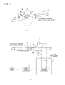
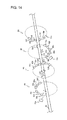
- Fig. 1 is a schematic view for explaining a basic principle and a basic configuration of the present invention.
- Fig. 1(a) is a perspective view schematically illustrating a light source 1 and light receiving elements 3a and 3b
- Fig. 1 (b) is a functional block diagram illustrating a wire surface inspection device according to the present invention.
- states of the light source 1 and the light receiving elements 3a and 3b as seen from the top are illustrated.
- the light from the light source 1 is processed by an optical processing portion (optical system) 2 to be inspecting light.
- the optical processing portion 2 is not illustrated.
- a cylindrical wire member 80 such as an insulated cable which is formed to extend in a wire shape is drawn to be wound at a high speed in the direction A illustrated in the figure.
- Inspection light beams 30a and 30b such as laser beams from the light source 1 are illuminated onto the surface of the wire 80, and the reflected light beams are received by light receiving elements 3a and 3b.
- the light receiving elements 3a and 3b are disposed at positions on a concentric circle, in the case where four or more light receiving elements are disposed, it is not necessary to dispose all the light receiving elements on the concentric circle, but any arrangement satisfying the above condition may be employed.
- the left and right light receiving elements in the width direction
- light receiving elements (not shown) which are not symmetrically disposed with respect to the width direction may be included.
- Output signals of the light receiving elements 3a and 3b which are symmetrically disposed with respect to the width direction are input to an addition processing portion 5 of a signal processing portion 4 to be added to each other.
- the output signal obtained from the addition is output to a defect detection portion 6.
- the defect detection portion 6 detects defect or stain based on whether or not the output signal is equal to or less than a predetermined threshold value. For example, if the stain or the defect exists, the reflected light decreases, so that the output signal of the light receiving element becomes weaker. Therefore, if the output signal is less than the threshold value, it is determined that the defect exists. Furthermore, the outputs of the light receiving elements which are not symmetrically disposed in the width direction are output to the defect detection portion 6 without use of the addition processing portion 5.
- the inspecting light beams 30a and 30b illuminated from the light source 1 alternately deviate from the wire 80. If the inspecting light beams 30a and 30b deviate from the wire 80, there is no reflected light. Therefore, although there is no defect or the like, the output signals of the light receiving elements 3a and 3b are equal to or less than the threshold value, which results in erroneous detection. However, since the left and right light receiving elements 3a and 3b are symmetrically disposed, the output signals of the light receiving elements 3a and 3b change alternately in the opposite directions due to the vibration, so that the output signals have symmetric waveforms.
- the vibration components can be offset by adding the two output signals.
- the influence on the detection of the vibration components can be suppressed by offsetting the changed amounts of the output signals that are generated due to the vibration of the wire 80 in the width direction by adding the output signals of the left and right symmetrically disposed light receiving elements, so that it is possible to accurately detect the defect such as scar (a bump, a cut, a foam, or the like) or the stain of the surface of the wire 80.
- a noise processing portion 7 such as a noise filter is provided at an upstream of the signal processing portion 4 or in front of the addition processing portion 5 in the signal processing portion 4 so that noise of the output signal is removed before the output signal is subject to the addition process.
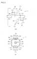
- Fig. 2 is a diagram illustrating arrangement of a light source and light receiving elements or the like of a wire surface inspection device according to an embodiment of the present invention.
- the signal processing portion 4 and the defect detection portion 6 are not illustrated in Figs. 2 to 15 .
- Fig. 2(a) is a side view illustrating the arrangement of the components of the wire surface inspection device 10 according to the embodiment of the present invention
- Fig. 2 (b) is a cross sectional view taken along line A-A'.
- Each of the light projecting portions 11 is a light source emitting an inspecting light beam 30.
- the light projecting portion (light source) 11 a laser and other light emitting devices may be used.
- the inspecting light beams 30 from the light projecting portions 11 are illuminated onto the inspection target wire 80 through an optical processing portion (optical system) 12 (12a and 12b), and the reflected light beams or the scattered light beams are sensed by light receiving portions 20 and 21.
- the optical system 12 (12a, 12b) is described later.
- the light receiving portions 20 and 21 are configured to include light receiving elements (hereinafter, referred to as "optical sensors") 20a to 20f, which are constructed with a plurality of optical sensors or the like, and optical sensors 21a to 21f.
- the light receiving portion 20 is disposed so as to surround the upper half portion of the circumference of the inspection target wire 80, and the light receiving portion 21 is disposed so as to surround the lower half portion thereof. Therefore, it is possible to inspect the entire surface of the front and rear (upper and lower) surfaces of the inspection target wire 80 without dead angle.
- Fig. 2(b) although the 12 optical sensors 20a to 20f and 21a to 21f are disposed in a concentric shape to surround the inspection target wire 80, as illustrated in Fig. 2(a) , with respect to the real positions of the optical sensors, the positions of the light receiving portion 20 and the light receiving portion 21 are disposed to be shifted in the longitudinal direction of the inspection target wire 80. In this manner, it is preferable that the positions of the light receiving portions 20 and 21 are disposed to be shifted from each other.
- the output signals of each pair of the optical sensors 20a and 20f, 20b and 20e, and 20c and 20d of the light receiving portion 20 are added to each other in the signal processing portion (refer to Fig. 1(b) ).
- the output signals of each pair of the optical sensors 21a and 21f, 21b and 21e, and 21c and 21d of the light receiving portion 21 are added to each other in the signal processing portion (refer to Fig. 1(b) ).
- the output signals of all the pairs of the symmetrically disposed optical sensors are not necessarily added to each other. Only the output signals of some pairs of the optical sensors may be added to each other, and the output signals of other optical sensors may be directly output to the defect detection portion 6. For example, only the output signals of the pair of the optical sensors 20a and 20f and the output signals of the pair of the optical sensors 21a and 21f may be added to each other, and other output signals may be directly output.
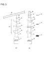
- Fig. 3 is a schematic view for explaining an example of a shaping process for inspecting light in an optical system according to the present invention.
- Fig. 3 (a) is a schematic view illustrating the optical system 12 as seen in the transverse direction of the inspection target wire 80 which is an inspection target.
- Fig. 3 (b) is a view illustrating the optical system 12 illustrated in Fig. 3(a) as seen from the just upper position or the just lower position (the side of the light source 11) of the inspection target wire 80.
- outer shapes of the inspecting light shaped by the optical system 12 are illustrated.
- the inspecting light 31 from the light projecting portion 11 such as a laser emitting device is incident onto the optical system 12.
- a cylindrical convex lens 13, a cylindrical concave lens 14, and a cylindrical convex lens 15 are arrayed in this order.
- the cylindrical convex lens is used so as to concentrate the focal point of the circular or elliptic parallel light in one axial direction.
- the cylindrical concave lens is used so as to convert the incident light, which is concentrated with a predetermined angle in one axial direction, into a parallel light.
- the laser beam generated by the light projecting portion 11 is an elliptic parallel light (inspecting light) 31 and is incident onto the cylindrical convex lens 13.
- the focal point of the incident parallel light 31 is concentrated by the cylindrical convex lens 13 so that the ellipse of the inspection target wire 80 is decreased in size in the long axis direction, and thus, the parallel light 31 is shaped into an horizontally-elongated thin elliptic light 32.
- the inspecting light 32 which is angled so as to concentrate the focal point thereof is allowed to return to the parallel light by the cylindrical concave lens 14.
- the inspecting light 33 which is allowed to return to the parallel light is concentrated again by a secondary cylindrical convex lens 15 in the long axis direction of the ellipse of the inspection target wire 80, so that the focal point of the inspecting light 33 can be adjust to the inspection target wire 80. Therefore, the short, thin slit-shaped inspecting light 35 which is formed to extend in the width direction is illuminated as a spot on the inspection target wire 80.
- the focal point of the inspecting light 35 is concentrated so as to be thin and sharp in the longitudinal direction of the inspection target wire 80.
- the original length of the inspecting light 35 in the width direction of the inspection target wire 80 is maintained. Therefore, the inspecting light 35 is illuminated as a horizontally-elongated thin slit-shaped beam on the inspection target wire 80.
- the inspecting light 35 which is shaped in a slit shape can be condensed so that the width in the short axis direction of the inspecting light 35 is equal to or less than 150 ⁇ m. Since the width of the inspecting light 35 is allowed to be equal to or less than 150 ⁇ m, it is possible to detect infinitesimal stain or the like which is beyond the visual detection limitation.
- the length of the long axis (the transverse direction length of the inspecting light) is sufficiently larger than the width (wire diameter) of the inspection target wire 80.
- the inspecting light 35 is shaped in such a manner that the long axis direction length of the ellipse is in a range of from 3 to 6 mm, and the length in the short axis direction is 200 ⁇ m or less.
- the wire diameter of the inspection target wire 80 is about 1 mm
- the long width of the beam-like inspecting light 35 is about 5 mm.
- the ratio (aspect ratio) of the width in the long axis direction to the width in the short axis direction of the ellipse of the inspecting light 35 is 30 or more.
- the vibration becomes strong in comparison with the case where the aspect ratio is 30.
- the power of the corresponding portion of the inspection target wire 80 decreases by half.
- the amplification ratio needs to be doubled. At this time, the ambient light or the electromagnetic noise increases twice, so that the S/N ratio of the inspection deteriorates.
- the aspect ratio is 60 or less.
- the outputs of the symmetrically disposed optical sensors are added to each other, so that the detection of the defect is achieved.
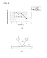
- Fig.4 illustrates the relationship between an illumination angle of inspecting light and a signal change rate.
- Fig. 4 (a) is a graph illustrating a change rate of a light receiving signal according to a change in the illumination angle ⁇ of the inspecting light 30, and
- Fig. 4 (b) is a view illustrating the illumination angle ⁇ with respect to the inspection target wire, which is the vertical axis of the graph of Fig. 4(a) .
- the change rate of the light receiving signal represents a change rate [(vl-v2) /v1] of the light receiving voltage v1 of the case where there is no stained point (reference black point) in the inspection target wire with respect to the light receiving voltage v2 of the case where there is a stained point.
- the higher signal change rate represents the higher stained point detection ability.
- the graph of the optical element 1 represents the measurement result of the optical sensor disposed just above the inspection target wire 80
- the graph of the optical element 2 represents the measurement result of the optical sensor which is disposed at the angle of 45° on the concentric circle to the reference point which is the point just above the inspection target wire 80.
- the change rate rapidly drops.
- the illumination angle ⁇ decreases, the transverse direction distance from the light projecting portion 11 to the light receiving portion 20 increases, so that the entire size of the inspection device increases.
- the illumination angle ⁇ is large.
- the illumination angle ⁇ is small. It can be understood from the graph of Fig. 4 (a) that, if the illumination angle ⁇ exceeds 70°, the detection ability deteriorates. Therefore, considering the miniaturization of the inspection device, it is preferable that the illumination angle ⁇ of the inspecting light 30 to the inspection target wire 80 is in a range of from 50° to 70° (incident angle of from 20° to 40°).
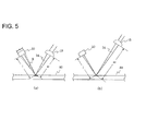
- Fig. 5 is a view for explaining a difference between the focal length of the light condensing lens 15 and the scattering range of the reflected light.
- Fig. 5(a) illustrates a case where the focal length a1 of the light condensing lens 15 is short
- Fig. 5 (b) illustrates a case where the focal length a2 is long.
- the longer focal length a2 illustrated in Fig. 5 (b) leads to the reduced scattering angle at the light receiving portion 20.
- the focal length of 50 mm since the reflected light spreads in a short distance , if the light receiving sensor is not closely disposed, the entire reflected light cannot be received.
- the focal length is 150 mm, since the reflected light spreads in a long distance, even though the light receiving sensor is disposed at a long distance, the entire reflected light can be received.
- the focal length of the light condensing lens 15 is preferably 100 mm or more and, in particular, more preferably, about 150 mm.
- the maximum value of a light condensing angle ⁇ of the reflected light is expressed by the following Equation.
- the angle is equal to or less than the light condensing angle ⁇ expressed by the following Equation, the light can be received by the light receiving sensor having the width w disposed at the distance 1.
- the light intensity P of the condensed inspecting light 35 has a Gaussian distribution indicated by the broken line 36 in Fig. 6 .
- the intensity P in the long axis direction of the ellipse of the inspecting light 35 indicated by the solid line 37 is uniformed by using diffraction type optical parts.
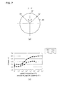
- Fig. 7 illustrates the relationship between positions of black points (indicated by the angle ⁇ ) on the circumference of the inspection target wire and light receiving voltages.
- Fig. 7 (a) is a conceptual view for explaining the angles ⁇ representing the positions of the black points (stained points) on the circumference.
- the position of the black point on the circumference of the inspection target wire 80 is defined by the angle ⁇ between the line from the center to the start point and the line from the center to the black point.
- the black points 82 and 83 are treated as the same position because the black points are symmetrically disposed. Therefore, 0° ⁇ 90°.
- the position of the black point in the width direction (on the circumference) is represented by the angle ⁇ shifted from the start point, that is, the position of the top of the inspection target wire 80.
- Fig. 7(b) is a graph illustrating the measurement results of the light receiving signals with respect to the positions of the black points.
- the graph illustrating the measurement results of the cases where the distances (optical paths) 1 from the inspection target wire 80 to the light receiving portion 20 are 11 mm and 17 mm, respectively. Since the angles ⁇ representing the positions of the black points are symmetric and the light receiving voltages thereof are the same, only the one measured side is illustrated in the graph.
- the amount of the reflected light decreases. Therefore, the amount of received light decreases and thus the output voltage of the light receiving portion 20 decreases. In other words, it is represented that, the lower the voltage, the higher the black point recognition sensitivity. Furthermore, the magnitude of the voltage of the light receiving signal is not a matter of interest, but the change amount of the light receiving signal caused by the difference between the positions of the black points is important.
- one light receiving portion 20 receives a positive reflected light in a range of from about 15° to about 22.5°. Therefore, if the inspection target wire 80 is rotated, there is no black point in the portion where the light receiving portion 20 receives the positive reflected light. Since the black point has a certain size, although the inspection target wire 80 is rotated by 15° to 22.5°, the black point does not completely disappear in the portion where the light receiving portion 20 receives the positive reflected light.
- the portion where the light receiving amount is uniform due to the rotation of the inspection target wire 80 since the black point completely disappears in the portion where the light receiving portion 20 receives the positive reflected light, the portion is regarded as the good part portion, and the recognition sensitivity for the black point is estimated according to the difference in the light receiving amount between the good part portion and the defective portion.
- the base level of the good part portion is about 6.5 V, and in the case where the distance (optical path) 1 from the inspection target wire 80 to the light receiving portion 20 is 17 mm, the base level of the good part portion is about 5.5 V.
- the sensitivity is the best in the angle range of from 0° to 20°, and the black point can be sufficiently detected until the angle of 35°. If the angle exceeds 40°, the change in voltage is small. In other words, the measurement result shows the tendency that, if the position of the black point is shifted toward the end, it is difficult to accurately detect the black point.
- plural light receiving sensors are disposed at a suitable angle interval around the axis of the inspection target wire so that the defect can be detected by the other sensors.
- the detection sensitivity varies depending on the position of the defect, and the reflection amount of the light varies, so that the base levels are different between the sensors. Therefore, it is more preferable that, in order to equalize the detection sensitivities of the sensors the base levels are adjusted to predetermined values, and the threshold values are set to different values according to the positions of the sensors.
- the method of adjusting the detection sensitivity there is a method of equalizing the levels (differences from the base levels) of the detection signals of the sensors in the case where the same defect is shifted in the circumferential direction by gain adjustment or the like and, after that, equalizing the base levels or a method of setting the threshold values according to the sensors so as to detect the same defect without adjustment of the detection signals.
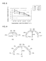
- Fig. 8 is a view illustrating measurement results of the change of the light receiving signal with respect to the magnitude of the transverse vibration of the inspection target wire.
- the vertical axis indicates the difference between the light receiving signal (output voltage) of the light receiving portion 20 in the case where there is no transverse vibration and the light receiving signal (output voltage) in the case where there is transverse vibration as the "signal change amount (V)," and the horizontal axis indicates the magnitude (amplitude) of the transverse vibration.
- the same shape and magnitude of the inspecting light 35 as the slit shape having a size of 5 mm x 0.15 mm described above are used.
- Figs. 9(a), 9(b) and 9 (c) illustrate that different numbers of light receiving sensors need to be used when the distances from the inspection target wire 80 to the light receiving sensors are changed, for example, 10 mm, 20 mm, and 30 mm.
- Fig. 9 illustrates the upper half portion, the same illustration may also apply to the lower half portion.
- Fig. 9(a) in the case where the distance is 10 mm, 4 light receiving sensors 20a to 20d are needed to cover the upper half portion of the inspection target wire 80 without dead angle, so that a total of 8 light receiving sensors are needed, including the light receiving sensors for the lower half portion.
- 6 light receiving sensors 20a to 20f are needed for the upper half portion, so that a total of 12 light receiving sensors are needed.
- 8 light receiving sensors 20a to 20h are needed for the upper half portion, so that a total of 16 light receiving sensors are needed.
- the distance 1 from the inspection target wire 80 increases, the more light receiving sensors are needed.
- the distance 1 from the inspection target wire 80 to the light receiving sensor is preferably in a range of from about 15 mm to about 20 mm.
- Fig. 10 (a) is a view illustrating the case where the optical sensors 20a to 20f are disposed to be perpendicular to the inspection target wire 80
- Fig. 10(b) is a view illustrating the case where the light receiving planes of the optical sensors 20a to 20f are disposed to be parallel to the inspection target wire 80.
- the light receiving elements 20a and 20d and the light receiving elements 20b and 20c make pairs of light receiving elements which are objects to be subjected to the addition process.
- the light receiving elements 20a and 20f, the light receiving elements 20b and 20e, and the light receiving elements 20c and 20d make pairs of light receiving elements which are objects to be subjected to the addition process.
- the arrangement of Fig. 9(b) the light receiving elements 20a and 20f, the light receiving elements 20b and 20e, and the light receiving elements 20c and 20d make pairs of light receiving elements which are objects to be subjected to the addition process.
- the light receiving elements 20a and 20h, the light receiving elements 20b and 20g, the light receiving elements 20c and 20f, and the light receiving elements 20d and 20e make pairs of light receiving elements which are objects to be subjected to the addition process.
- the description about which light receiving elements make respective pairs is not given in the following examples.
- the positions of a plurality of inspection unit sets, each including the light projecting portion 11, the optical system 12, and the light receiving portion 20, are disposed to be shifted in the longitudinal direction of the inspection target wire 80 and the angles are shifted from one another in the axial direction of the inspection target wire 80.
- Such arrangement of shifting in the longitudinal direction is effective in preventing the negative influence caused when the reflected lights of the inspecting lights of different sets are incident onto to the light receiving portions of other sets.
- a set of two inspection units a set of arbitrary number of inspection units such as a set of three, four, five, or six inspection units may be provided.
- a set of three inspection units it is preferable that the positions of the inspection units in the longitudinal direction are shifted from one other, and the arrangement angle with respect to the axial direction of the inspection target wire 80 is shifted by 120°.
- the arrangement angle of the case of using the four inspection units is shifted by 90°; the arrangement angle of the case of using the five inspection units is shifted by 72°; and the arrangement angle of the case of using the six inspection units is shifted by 60°.
- Fig. 11 illustrates an example of arrangement of inspection units in the case where a set of four inspection units 51 to 54 is provided.
- each of the inspection units 51 to 54 illustrates four optical sensors, and each of the inspection units 51 to 54 covers a range of about 150°.
- Fig. 11(a) is a schematic view illustrating a wire surface inspection device including a set of four inspection units 51 to 54 as seen from the side
- Fig. 11(b) is a cross sectional view taken along line A-A'.
- the inspection units 51 to 54 include four optical sensors 22a to 22d, 23a to 23d, 24a to 24d, and 25a to 25d, respectively.
- the inspection units 51 to 54 are disposed so that the end portions of the optical sensors overlap each other. Therefore, it is possible to increase accuracy of detection of the defect of the end portion of the inspecting light. It is preferable that the adjacent inspection units among the inspection units 51 to 54 are disposed to be separated from each other by a distance of from about 100 mm to about 200 mm in order to prevent the influence of the inspecting light beams.
- Fig. 12 illustrates another example of arrangement of the optical sensors.
- six optical sensors 20a to 20f similar to those illustrated in Fig. 10 are deposed to cover 200° of the circumference of the inspection target wire 80. Therefore, it is possible to detect the reflected light of the inspection target wire 80 without loss.
- Fig. 12 although only one set of the optical sensors are illustrated, two sets, three sets, four sets, or desired number of sets of the optical sensors may be disposed so that the optical sensors in such an arrangement are disposed to cover the circumference of the inspection target wire 80.
- Fig. 13 illustrates still another example of arrangement of the optical sensors.
- six optical sensors 20a to 20f similar to those of Fig. 12 are used.
- detection portions 25 of the optical sensors 20a to 20f are illustrated.
- Fig. 13 (a) illustrates the same arrangement state as that of Fig. 12
- Fig. 13(b) illustrate an arrangement state where positions of some optical sensors, that is, the optical sensors 20b and 20e are shifted.
- each of the detection portions 25 of the optical sensors 20a to 20f is slightly smaller than the optical sensor in the outer shape, if the optical sensors 20a to 20f are disposed so as for the front surfaces of the optical sensors to abut one another as illustrated in Fig. 13 (a) , non-detected zones 41 exists between the detection portions 25 of the adjacent optical sensors
- the non-detected zones 41 are decreased. In this manner, it is possible to decrease the non-detected zones 41 by shifting the positions of the optical sensors towards the inspection target wire 80. In addition, it is also possible to adjust the sensitivity of the optical sensor by changing the distance from the inspection target wire 80 to the optical sensor.
- Fig. 13 (b) although the case where the positions of the optical sensors 20b and 20e are shifted is illustrated, it is also possible to decrease some of the non-detected zones 41 by shifting the positions of other optical sensors (for example, 20c and 20d). In the example illustrated in Fig. 13 , as illustrated in Fig. 13(b) , it is most efficient to shift the positions of the optical sensors 20b and 20e. However, which optical sensors are to be shifted in position is an optional configuration which can be appropriately changed according to the structure or the like of the apparatus.
- the inspecting light may be shaped into a thin slit-shaped inspecting light by using a transmitting light of a thin slit obtained by illuminating the inspecting light from the light source on the thin slit (a slit having a width of about 100 micron to several hundred micron).
- the light source a light source (for example, LED or the like) other than the laser may be used besides the laser source.
- the output light is a parallel light.
- the light source is disposed at a focal point portion of a parabolic reflecting mirror (paraboloidal mirror), so that it is possible to output the parallel light as a reflected light of the paraboloidal mirror.
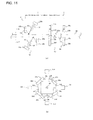
- Fig. 14 illustrates still another embodiment of the present invention.
- four inspection units 60 to 63 are disposed around the wire 80 in an equal interval.
- the inspection units 60 to 63 are disposed to be shifted in the axial direction so as not to be overlapped. In this manner, the range of 360° is detected by the four inspection units 60 to 63, so that it is possible to securely inspect the entire circumference.
- Each of the inspection units 60 to 63 includes six light receiving elements (three sets) (60a to 60f, 61a to 61f, 62a to 62f, and 63a to 63f) which are symmetrically disposed in the axial direction. Therefore, it is possible to accurately detect the reflected light of the inspection range of each of the inspection units 60 to 63. In order to accurately detect the defect of the surface of the wire 80, it is preferable that the four inspection units 60 to 63 and the six light receiving elements (three sets) are disposed in this manner.
- the outputs of the light receiving elements 60a and 60f, the outputs of the light receiving elements 60b and 60e, and the outputs of the light receiving elements 60c and 60d are added respectively, and after that, are output to the defect detection portion 6 (refer to Fig. 1(b) ).
- the outputs of only one set, for example, only the light receiving elements 60a and 60f may be added to each other. In this case, the outputs that are not added are directly output to the defect detection portion 6.
- the process for the output signals of the light receiving elements of the other inspection units 61 to 63 is also the same as that of the inspection unit 60.
- Fig. 15 is a graph illustrating the output signals of the light receiving elements 60a to 60f of the inspection unit 60 illustrated in Fig. 14 .
- the graph illustrates the output signals when the vibration occurs in the portion where there is no defect.
- the light receiving elements 60a and 60f, the light receiving elements 60b and 60e, and the light receiving elements 60c and 60d have substantially symmetric waveforms, respectively. Therefore, by adding outputs of the corresponding light receiving elements in each pair, it is possible to cancel the vibration components.
Landscapes
- Physics & Mathematics (AREA)
- Health & Medical Sciences (AREA)
- Life Sciences & Earth Sciences (AREA)
- Chemical & Material Sciences (AREA)
- Analytical Chemistry (AREA)
- Biochemistry (AREA)
- General Health & Medical Sciences (AREA)
- General Physics & Mathematics (AREA)
- Immunology (AREA)
- Pathology (AREA)
- Engineering & Computer Science (AREA)
- Textile Engineering (AREA)
- Investigating Materials By The Use Of Optical Means Adapted For Particular Applications (AREA)
Abstract
Description
- The present invention relates to a defect inspection device which inspects various types of defects such as stain and unevenness of the surface of a wire member, and more particularly, to a wire surface inspection device which inspects defects existing on the surface of a wire member provided with a coating layer such as an insulating layer thereon.
- Concomitantly with an increasing export of wire elements such as multi-layered insulated cable for use in transformers or the like incorporated in mobile phones or game machines, visual inspection on the appearance of the wire elements has been strictly performed by customers. Recently, there is a demand on that infinitesimal stain or scar is strictly checked. As a wire surface inspection device which inspects unevenness or scars of the surface of a wire element, there has been disclosed a device with a plurality of light projectors that is disposed around a wire element so as to illuminate the wire element in the slanted direction with respect to the central axis line of the wire element, in order to detect defects on a peripheral portion of the wire element (refer to Patent Document 1). There has been also disclosed a wire surface inspection device with two laser sources that are allowed to illuminate the entire circumference of the wire element with inspecting light, without dead angles (refer to Patent Document 2).
- Patent Document 1: Japanese Utility Model Application Laid-Open (JU-A) No.
49-013688 - Patent Document 2: Japanese Patent Application Laid-Open (JP-A) No.
10-68700 - However, in the technologies disclosed in
Patent Documents - In addition, due to the vibration of an inspection target wire in the width direction (the direction perpendicular to the axial direction), there occurs a phenomenon where the inspecting light illuminated onto a peripheral portion of the inspection target wire subtly collides with the wire element or not. Therefore, since the reflected light incident onto the light receiving element greatly varies, the vibration in the width direction results in erroneous detection.
- The present invention is made in view of the problems in the related art and is to provide a wire surface inspection device capable of accurately detecting a defect such as a scar (a bump, a cut, a foam, or the like), a stain, or discoloration of the surface of a wire element (hereinafter, referred to as a " wire") which is formed to extend in a wire shape by preventing erroneous detection attributable to the vibration of the inspection target wire.
- In order to solve the aforementioned problems, in the present invention, a plurality of light receiving elements is symmetrically disposed in the width direction of an inspection target wire, and vibration components in the width direction of the inspection target wire can be offset by a process of calculating output signals from the light receiving elements that are symmetrically disposed.
- According to a first aspect of the present invention, there is provided a wire surface inspection device including: a light source which outputs inspecting light onto the surface of an inspection target wire; an optical processing portion which allows the inspecting light output from the light source to illuminate the surface of the inspection target wire; a light receiving portion where at least two light receiving elements which receive reflected light of the inspecting light from the inspection target wire are disposed around the inspection target wire at substantially symmetric positions with respect to a central axis of the inspection target wire and a plane having the central axis of the inspection target wire thereon; and a defect detection portion which performs a calculation process on output signals of the symmetrically-disposed light receiving elements and detects a defect of the surface of the inspection target wire based on the calculated result of the output signals.
- In the aspect, the vibration noise is removed from the output signal by performing calculation (for example, addition, subtraction, differentiation, integration, or the like) on the output signals of the light receiving elements which are symmetrically disposed in the width direction of the inspection target wire, so that it is possible to prevent the erroneous detection attributable to the vibration of the inspection target wire in the width direction. Furthermore, since there is no likelihood that the reflected light comes to deviate from the wire due to the vibration, the longitudinal direction component of the vibration (long-side direction vibration component) of the inspection target wire is not substantially influenced from the vibration. Therefore, the longitudinal direction component of the vibration of the inspection target wire can be neglected.
- According to a second aspect of the present invention, in the wire surface inspection device according to the first aspect, n sets of inspection units, each set including the light source, the optical processing portion, and the light receiving portion, are disposed at an interval of equally n-divided angles of the circumference of the inspection target wire (n is an integer equal to two or more).
- In the aspect, plural inspection unit sets are disposed to surround the inspection target wire. When one set of inspection units is used, there is a limitation in the inspection range by the inspecting light which can be illuminated from the light source. Therefore, the plural inspection units are disposed to surround the inspection target wire, so that the entire surface of the inspection target wire can be inspected. For example, in the case where the entire angle is divided into four angle ranges, if each inspection unit securely covers the angle of 90° (+45°), the detection can be achieved over the entire angle range of 360°.
- If the coverage range of one set of inspection units is 90°, very accurate detection can be obtained. For example, if the defect is located at the position shifted by ±60° from the front position of the light source (laser) (that is, the position of the end portion in the case where the sensors are disposed at the interval of 120°), the change amount of the reflected light decreases at the end portion, so that it is difficult to detect the defect. However, according to this aspect, if the defect is located at the position shifted by about ±45° (that is, at the position of the end portion in the case where the sensors are disposed at the interval of 90°), the change amount of the reflected light also increases, so that it is possible to detect the defect with high accuracy.
- According to a third aspect of the present invention, in the wire surface inspection device according to the first or second aspect, the optical processing portion shapes the inspecting light into a thin slit shape by concentrating the focal point of the inspecting light output from the light source so that the short axis thereof is aligned with the longitudinal direction of the inspection target wire and allows the inspecting light to illuminate the inspection target wire.
- In the aspect, the inspecting light is shaped into a thin slit shape by concentrating the focal point of the inspecting light in the longitudinal direction of the inspection target wire. In this manner, the resolution in the longitudinal direction of the inspection target wire can be increased by concentrating the short axis of the inspecting light into a thin slit shape, so that it is possible to detect the defect (discoloration, a stain, a scar, or the like) which is small in size in the longitudinal direction.
- According to a fourth aspect of the present invention, in the wire surface inspection device according to any one of the first to third aspects, the optical processing portion includes: a cylindrical convex lens which concentrates a focal point of the inspecting light in the short axis direction; a cylindrical concave lens which converts the concentrated inspecting light into a parallel light; and a light condensing lens which further concentrates the focal point of the parallel light-converted inspecting light in the short axis direction and allows the inspecting light as a slit-shaped spot light to illuminate the inspection target wire.
- According to the aspect, since parallel light or nearly-parallel light is illuminated as the inspecting light, the reflected light does not spread and the entire reflected light can be received by the light receiving sensor even though the light receiving sensor has a small size. Therefore, the light reception sensitivity improves. In addition, after the ellipse parallel light is formed one time, the concentration is performed and the light can be concentrated into the thinner slit-shaped beam.
- In other words, according to the aspect, it is possible to further concentrate the focal point in the short axis direction (longitudinal direction of the inspection target wire) of the inspecting light while suppressing the spreading of the inspecting light. Finally, the length in the short axis direction of the inspecting light can be decreased to several hundreds micrometers, for example, to about 100 to 150 micrometers. In this manner, by reducing the length of the inspecting light to about 100 to 150 micrometers, it is possible to detect infinitesimal defects having the order of 100 micrometers.
- According to a fifth aspect of the present invention, in the wire surface inspection device according to any one of the first to fourth aspects, the optical processing portion performs a shaping process of shaping the inspecting light into a substantial elliptic shape having a long axis in a short side direction of the inspection target wire.
- According to a sixth aspect of the present invention, in the wire surface inspection device according to any one of the first to fifth aspects, the signal processing portion adds the output signals of at least the two light receiving elements.
- In the aspect, the vibration noise is removed from the output signal by offsetting the vibration components in the width direction by adding the output signals of the of the light receiving elements which are symmetrically disposed in the width direction of the inspection target wire, so that it is possible to prevent the erroneous detection attributable to the vibration in the width direction of the inspection target wire. Furthermore, since the reflected light des not deviate from the wire due to the vibration, the longitudinal direction component of the vibration (longitudinal direction vibration component) of the inspection target wire is not substantially influenced from the vibration. Therefore, the longitudinal direction component of the vibration of the inspection target wire can be neglected.
- According to a seventh aspect of the present invention, in the wire surface inspection device according to any one of the first to fifth aspects, a ratio of the long diameter and the short diameter of the substantial elliptic shape is 30 or more.
- In the wire surface inspection device according to the firth aspect of the present invention, the vibration noise is removed from the output signal by performing calculation (for example, addition, subtraction, differentiation, integration, or the like) on the output signals of the light receiving elements which are symmetrically disposed in the width direction of the inspection target wire, so that it is possible to prevent the erroneous detection attributable to the vibration in the width direction of the inspection target wire.
- In the wire surface inspection device according to the second aspect of the present invention, plural inspection unit sets are disposed to surround the inspection target wire. In one inspection unit set, there is a limitation in the range of the inspecting light which can be illuminated from the light source. Therefore, plural inspection unit sets are disposed to surround the inspection target wire, so that the entire surface of the inspection target wire can be inspected.
- In the wire surface inspection device according to the third aspect of the present invention, the inspecting light is shaped into a thin slit shape by concentrating the focal point of the inspecting light in the longitudinal direction of the inspection target wire. In this manner, the resolution in the longitudinal direction of the inspection target wire can be increased by concentrating the short axis of the inspecting light into a thin slit shape, so that it is possible to detect defects (discoloration, a stain, a scar, or the like) which are small in the longitudinal direction.
- In the wire surface inspection device according to a fourth aspect of the present invention, since parallel light or nearly-parallel light is illuminated as the inspecting light, the reflected light does not spread and thus the entire reflected light can be received by the light receiving sensor even though the light receiving sensor has a small size. Therefore, the light reception sensitivity improves. In addition, after the ellipse parallel light is formed one time, the concentration is performed and the light can be concentrated into the thinner slit-shaped beam. In other words, according to the aspect, it is possible to further concentrate the focal point in the short axis direction of the inspecting light (that is, longitudinal direction of the inspection target wire) while suppressing the spreading of the inspecting light.
- In the wire surface inspection device according to the fifth aspect of the present invention, in the case of surface inspection of the inspection target wire, it is possible to detect stain, scar, or the like even though the inspection target wire slightly vibrates in the transverse direction.
- In the wire surface inspection device according to the sixth aspect of the present invention, the vibration noise is removed from the output signal by offsetting the vibration components in the width direction by adding the output signals of the of the light receiving elements which are symmetrically disposed in the width direction of the inspection target wire, so that it is possible to prevent the erroneous detection attributable to the vibration of the inspection target wire in the width direction.
- In a wire surface inspection device according to the seventh aspect of the present invention, in the case of surface inspection of the inspection target wire, it is possible to detect stain, scar, or the like even though the inspection target wire slightly vibrates in the transverse direction.
-
-
Fig. 1 is a schematic view for explaining a basic principle and a basic configuration of the present invention. -
Fig. 2 is a schematic view illustrating the appearance of a wire surface inspection device according to an embodiment of the present invention. -
Fig. 3 is a diagram for explaining an example of a shaping process for inspecting light using an optical system according to the present invention. -
Fig. 4 is a diagram for explaining the relationship between an illumination angle of inspecting light and a signal change rate. -
Fig. 5 is a diagram for explaining a focal length of a light condensing lens and a difference of a scattering range of a reflected light. -
Fig. 6 is a diagram for explaining equalization of light intensities in a long axis direction of the ellipse-shaped inspecting light by using a refraction type optical part. -
Fig. 7 is a diagram illustrating the relationship between a position of a stained point (represented by an angle β) of an inspection target wire in the width direction and a light receiving voltage. -
Fig. 8 is a diagram illustrating measurement results of transverse vibration amount of inspection target wires and a change in a light receiving signal. -
Fig. 9 is a diagram for explaining the number of light receiving sensors in the cases a distance from an inspection target wire to a light receiving device varies, for example, 10 mm, 20 mm, and 30 mm, respectively. -
Fig. 10 is a diagram for explaining a decrease in gap (non-detected zone) between adjacent optical sensors, the decrease being achieved by slanting optical sensors in the rear side. -
Fig. 11 is a diagram illustrating an example of arrangement of inspection units in the case where a set of four inspection units is disposed. -
Fig. 12 is a diagram illustrating another example of arrangement of optical sensors. -
Fig. 13 is a diagram illustrating still another example of arrangement of optical sensors for decreasing a non-detected zone. -
Fig. 14 is a diagram illustrating another embodiment of the present invention. -
Fig. 15 is a graph illustrating output signals of six light receiving elements in one inspection unit according to the embodiment illustrated inFig. 14 . -
- 10: wire surface inspection device
- 11: light projecting portion
- 12: optical system (optical processing portion)
- 13: cylindrical convex lens
- 14: cylindrical concave lens
- 15: secondary cylindrical convex lens (light condensing lens)
- 20 to 25: light receiving portion
- 20a to 20f, 21a to 21f, 22a to 22d, 23a to 23d, 24a to 24d, 25a to 25f: optical sensor (optical element)
- 25: detection portion
- 30, 31, 32, 33, 34, 35: inspecting light
- 40, 41: non-detected zone
- 51 ∼ 54, 60 ∼ 63: inspection unit
- 80: inspection target wire
- Hereinafter, embodiments of the present invention will be described in detail.
Fig. 1 is a schematic view for explaining a basic principle and a basic configuration of the present invention.Fig. 1(a) is a perspective view schematically illustrating alight source 1 andlight receiving elements Fig. 1 (b) is a functional block diagram illustrating a wire surface inspection device according to the present invention. InFig. 1(b) , states of thelight source 1 and thelight receiving elements Fig. 1(b) , the light from thelight source 1 is processed by an optical processing portion (optical system) 2 to be inspecting light. However, inFig. 1(a) , theoptical processing portion 2 is not illustrated. - A cylindrical wire member 80 (hereinafter, referred to as a "
wire 80") such as an insulated cable which is formed to extend in a wire shape is drawn to be wound at a high speed in the direction A illustrated in the figure.Inspection light beams light source 1 are illuminated onto the surface of thewire 80, and the reflected light beams are received bylight receiving elements light receiving elements wire 80 is set as a reference line and that the optical paths from thelight source 1 to thelight receiving elements - Furthermore, in
Fig. 1(a) , although thelight receiving elements - Output signals of the
light receiving elements signal processing portion 4 to be added to each other. The output signal obtained from the addition is output to adefect detection portion 6. Thedefect detection portion 6 detects defect or stain based on whether or not the output signal is equal to or less than a predetermined threshold value. For example, if the stain or the defect exists, the reflected light decreases, so that the output signal of the light receiving element becomes weaker. Therefore, if the output signal is less than the threshold value, it is determined that the defect exists. Furthermore, the outputs of the light receiving elements which are not symmetrically disposed in the width direction are output to thedefect detection portion 6 without use of the addition processing portion 5. - However, in the case where the
wire 80 vibrates in the transverse direction, as easily expected fromFig. 1(b) , if the vibration width is large, the inspectinglight beams light source 1 alternately deviate from thewire 80. If the inspectinglight beams wire 80, there is no reflected light. Therefore, although there is no defect or the like, the output signals of thelight receiving elements light receiving elements light receiving elements - Therefore, the vibration components can be offset by adding the two output signals. In this manner, in the present invention, the influence on the detection of the vibration components can be suppressed by offsetting the changed amounts of the output signals that are generated due to the vibration of the
wire 80 in the width direction by adding the output signals of the left and right symmetrically disposed light receiving elements, so that it is possible to accurately detect the defect such as scar (a bump, a cut, a foam, or the like) or the stain of the surface of thewire 80. - In addition, it is preferable that a
noise processing portion 7 such as a noise filter is provided at an upstream of thesignal processing portion 4 or in front of the addition processing portion 5 in thesignal processing portion 4 so that noise of the output signal is removed before the output signal is subject to the addition process. - Hereinafter, the embodiments of the present invention will be described in detailed with reference to
Figs. 2 and15 .Fig. 2 is a diagram illustrating arrangement of a light source and light receiving elements or the like of a wire surface inspection device according to an embodiment of the present invention. In the hereinafter description, thesignal processing portion 4 and thedefect detection portion 6 are not illustrated inFigs. 2 to 15 .Fig. 2(a) is a side view illustrating the arrangement of the components of the wiresurface inspection device 10 according to the embodiment of the present invention, andFig. 2 (b) is a cross sectional view taken along line A-A'. - Each of the light projecting portions 11 (11a and 11b) is a light source emitting an inspecting
light beam 30. As the light projecting portion (light source) 11, a laser and other light emitting devices may be used. The inspectinglight beams 30 from thelight projecting portions 11 are illuminated onto theinspection target wire 80 through an optical processing portion (optical system) 12 (12a and 12b), and the reflected light beams or the scattered light beams are sensed by light receivingportions - The
light receiving portions optical sensors 21a to 21f. Thelight receiving portion 20 is disposed so as to surround the upper half portion of the circumference of theinspection target wire 80, and thelight receiving portion 21 is disposed so as to surround the lower half portion thereof. Therefore, it is possible to inspect the entire surface of the front and rear (upper and lower) surfaces of theinspection target wire 80 without dead angle. - In
Fig. 2(b) , although the 12optical sensors 20a to 20f and 21a to 21f are disposed in a concentric shape to surround theinspection target wire 80, as illustrated inFig. 2(a) , with respect to the real positions of the optical sensors, the positions of thelight receiving portion 20 and thelight receiving portion 21 are disposed to be shifted in the longitudinal direction of theinspection target wire 80. In this manner, it is preferable that the positions of thelight receiving portions light projecting portion 11b onto thelight receiving portion 20 and to prevent the inspecting light incident from the otherlight projecting portion 11a onto thelight receiving portion 21, so that the light receiving portion is not influenced by the other inspecting light. - The output signals of each pair of the
optical sensors light receiving portion 20 are added to each other in the signal processing portion (refer toFig. 1(b) ). Similarly, the output signals of each pair of theoptical sensors light receiving portion 21 are added to each other in the signal processing portion (refer toFig. 1(b) ). In addition, the output signals of all the pairs of the symmetrically disposed optical sensors are not necessarily added to each other. Only the output signals of some pairs of the optical sensors may be added to each other, and the output signals of other optical sensors may be directly output to thedefect detection portion 6. For example, only the output signals of the pair of theoptical sensors optical sensors -
Fig. 3 is a schematic view for explaining an example of a shaping process for inspecting light in an optical system according to the present invention.Fig. 3 (a) is a schematic view illustrating theoptical system 12 as seen in the transverse direction of theinspection target wire 80 which is an inspection target.Fig. 3 (b) is a view illustrating theoptical system 12 illustrated inFig. 3(a) as seen from the just upper position or the just lower position (the side of the light source 11) of theinspection target wire 80. In the right side ofFig. 3(b) , outer shapes of the inspecting light shaped by theoptical system 12 are illustrated. - The inspecting light 31 from the
light projecting portion 11 such as a laser emitting device is incident onto theoptical system 12. In theoptical system 12, a cylindricalconvex lens 13, a cylindricalconcave lens 14, and a cylindricalconvex lens 15 are arrayed in this order. The cylindrical convex lens is used so as to concentrate the focal point of the circular or elliptic parallel light in one axial direction. The cylindrical concave lens is used so as to convert the incident light, which is concentrated with a predetermined angle in one axial direction, into a parallel light. - The laser beam generated by the
light projecting portion 11 is an elliptic parallel light (inspecting light) 31 and is incident onto the cylindricalconvex lens 13. The focal point of the incidentparallel light 31 is concentrated by the cylindricalconvex lens 13 so that the ellipse of theinspection target wire 80 is decreased in size in the long axis direction, and thus, theparallel light 31 is shaped into an horizontally-elongated thinelliptic light 32. - Next, the inspecting
light 32 which is angled so as to concentrate the focal point thereof is allowed to return to the parallel light by the cylindricalconcave lens 14. The inspectinglight 33 which is allowed to return to the parallel light is concentrated again by a secondary cylindricalconvex lens 15 in the long axis direction of the ellipse of theinspection target wire 80, so that the focal point of the inspectinglight 33 can be adjust to theinspection target wire 80. Therefore, the short, thin slit-shaped inspecting light 35 which is formed to extend in the width direction is illuminated as a spot on theinspection target wire 80. - In other words, as illustrated in
Figs. 3 (a) and (b) , the focal point of the inspectinglight 35 is concentrated so as to be thin and sharp in the longitudinal direction of theinspection target wire 80. However, as illustrated inFig. 3(b) , the original length of the inspectinglight 35 in the width direction of theinspection target wire 80 is maintained. Therefore, the inspectinglight 35 is illuminated as a horizontally-elongated thin slit-shaped beam on theinspection target wire 80. - In this manner, by modifying the inspecting light into the thin slit-shaped beam by concentrating the focal point of the one axis of the inspecting light, it is possible to increase an S/N ratio at the time of detecting the stain, the scar, or the like of the inspection target wire, so that it is possible to detect infinitesimal stain or the like. For example, the inspecting
light 35 which is shaped in a slit shape can be condensed so that the width in the short axis direction of the inspectinglight 35 is equal to or less than 150 µm. Since the width of the inspectinglight 35 is allowed to be equal to or less than 150µm, it is possible to detect infinitesimal stain or the like which is beyond the visual detection limitation. - It is preferable that, in the ellipse of the inspecting
light 35 shaped in a slit shape, the length of the long axis (the transverse direction length of the inspecting light) is sufficiently larger than the width (wire diameter) of theinspection target wire 80. In addition, it is more preferable that the inspectinglight 35 is shaped in such a manner that the long axis direction length of the ellipse is in a range of from 3 to 6 mm, and the length in the short axis direction is 200 µm or less. For example, it is preferable that, if the wire diameter of theinspection target wire 80 is about 1 mm, the long width of the beam-like inspectinglight 35 is about 5 mm. - In addition, from the defection size (150 µm) which is to be detected and the size (5 mm) of the light emitted from the light source, 5÷0.15≒30, and thus, it is preferable that the ratio (aspect ratio) of the width in the long axis direction to the width in the short axis direction of the ellipse of the inspecting
light 35 is 30 or more. In addition, for example, in the case where the aspect ratio is 60, the vibration becomes strong in comparison with the case where the aspect ratio is 30. However, since the beam spreads, the power of the corresponding portion of theinspection target wire 80 decreases by half. - As the power decreases, the amount of signal change due to the defect decreases. Therefore, the amplification ratio needs to be doubled. At this time, the ambient light or the electromagnetic noise increases twice, so that the S/N ratio of the inspection deteriorates. In addition, it is necessary to broaden the beam of the light source and thus the lens needs to be added. In addition, it is necessary to increase the sizes of the lens and mirror and thus the head increases in size. In addition, since only the central portion of the beam is used but other portions are not, the loss in energy increases. From the viewpoint of the trade-off relationship, it is preferable that the aspect ratio is 60 or less.
- Therefore, in the case where the surface inspection is performed during the extraction of the
inspection target wire 80, although there is a small vibration of theinspection target wire 80 in the transverse direction, stain, scar, or the like can be detected. - However, when the transverse vibration is large, since the output signal is influenced by the vibration, it may be difficult to accurately detect the stain, scar, or the like. According to the present invention, in order to more securely prevent the influence of the transverse vibration, the outputs of the symmetrically disposed optical sensors are added to each other, so that the detection of the defect is achieved.
- With respect to the illumination angle of the inspecting light from the
light projecting portion 11, an appropriate angle exists.Fig.4 illustrates the relationship between an illumination angle of inspecting light and a signal change rate.Fig. 4 (a) is a graph illustrating a change rate of a light receiving signal according to a change in the illumination angle α of the inspectinglight 30, andFig. 4 (b) is a view illustrating the illumination angle α with respect to the inspection target wire, which is the vertical axis of the graph ofFig. 4(a) . Herein, the graph ofFig. 4 (a) illustrates the change rate of the light receiving signal when changing the illumination angle α (incident angle=90-α) of the inspectinglight 30 illuminated from thelight projecting portion 11 to theinspection target wire 80. In addition, the change rate of the light receiving signal represents a change rate [(vl-v2) /v1] of the light receiving voltage v1 of the case where there is no stained point (reference black point) in the inspection target wire with respect to the light receiving voltage v2 of the case where there is a stained point. The higher signal change rate represents the higher stained point detection ability. The graph of theoptical element 1 represents the measurement result of the optical sensor disposed just above theinspection target wire 80, and the graph of theoptical element 2 represents the measurement result of the optical sensor which is disposed at the angle of 45° on the concentric circle to the reference point which is the point just above theinspection target wire 80. - According to the measurement result, at the angle where the illumination angle α is larger than 70°, the change rate rapidly drops. In addition, if the illumination angle α decreases, the transverse direction distance from the
light projecting portion 11 to thelight receiving portion 20 increases, so that the entire size of the inspection device increases. In terms of the miniaturization of the device, it is preferable that the illumination angle α is large. However, in terms of the defect detection ability, it is preferable that the illumination angle α is small. It can be understood from the graph ofFig. 4 (a) that, if the illumination angle α exceeds 70°, the detection ability deteriorates. Therefore, considering the miniaturization of the inspection device, it is preferable that the illumination angle α of the inspectinglight 30 to theinspection target wire 80 is in a range of from 50° to 70° (incident angle of from 20° to 40°). - In addition, the relationship between the position of the light receiving sensor and the focal length of the light condensing lens (cylindrical convex lens) 15 of the
optical system 12 is described with reference toFig. 5. Fig. 5 is a view for explaining a difference between the focal length of thelight condensing lens 15 and the scattering range of the reflected light.Fig. 5(a) illustrates a case where the focal length a1 of thelight condensing lens 15 is short, andFig. 5 (b) illustrates a case where the focal length a2 is long. - As clarified from
Fig. 5 , it can be understood that, when thedistances 1 to thelight receiving portions 20 is set to be the same, the longer focal length a2 illustrated inFig. 5 (b) leads to the reduced scattering angle at thelight receiving portion 20. For example, in the case where the focal length of 50 mm, since the reflected light spreads in a short distance , if the light receiving sensor is not closely disposed, the entire reflected light cannot be received. On the contrary, in the case where the focal length is 150 mm, since the reflected light spreads in a long distance, even though the light receiving sensor is disposed at a long distance, the entire reflected light can be received. - As a result of experiments, it can be understood that, in the case where general light receiving sensors are used, if the distance from the
inspection target wire 80 to thelight receiving portion 20 is in a range of from 10 mm to 20 mm, the focal length of thelight condensing lens 15 is preferably 100 mm or more and, in particular, more preferably, about 150 mm. - When the distance 1 (optical path) from the
inspection target wire 80 to thelight receiving portion 20 and the width w of the light receiving plane illustrated inFig. 5(a) are set to be the same, the maximum value of a light condensing angle θ of the reflected light is expressed by the following Equation. In other words, if the angle is equal to or less than the light condensing angle θ expressed by the following Equation, the light can be received by the light receiving sensor having the width w disposed at thedistance 1.
- In addition, the light intensity P of the condensed inspecting
light 35 has a Gaussian distribution indicated by thebroken line 36 inFig. 6 . Herein, it is preferable that the intensity P in the long axis direction of the ellipse of the inspectinglight 35 indicated by thesolid line 37 is uniformed by using diffraction type optical parts. -
Fig. 7 illustrates the relationship between positions of black points (indicated by the angle β) on the circumference of the inspection target wire and light receiving voltages.Fig. 7 (a) is a conceptual view for explaining the angles β representing the positions of the black points (stained points) on the circumference. In the case where the position of the top of the inspection target wire 80 (position of the black point 81) as seen from thelight projecting portion 11 is set as a start point β=0°), the position of the black point on the circumference of theinspection target wire 80 is defined by the angle β between the line from the center to the start point and the line from the center to the black point. Theblack points 82 and 83 are treated as the same position because the black points are symmetrically disposed. Therefore, 0°≤β≤90°. In other words, the position of the black point in the width direction (on the circumference) is represented by the angle β shifted from the start point, that is, the position of the top of theinspection target wire 80. -
Fig. 7(b) is a graph illustrating the measurement results of the light receiving signals with respect to the positions of the black points. The graph illustrating the measurement results of the cases where the distances (optical paths) 1 from theinspection target wire 80 to thelight receiving portion 20 are 11 mm and 17 mm, respectively. Since the angles β representing the positions of the black points are symmetric and the light receiving voltages thereof are the same, only the one measured side is illustrated in the graph. - If there is a black point, illuminated light energy is absorbed, so that the amount of the reflected light decreases. Therefore, the amount of received light decreases and thus the output voltage of the
light receiving portion 20 decreases. In other words, it is represented that, the lower the voltage, the higher the black point recognition sensitivity. Furthermore, the magnitude of the voltage of the light receiving signal is not a matter of interest, but the change amount of the light receiving signal caused by the difference between the positions of the black points is important. - When the position of the
light receiving portion 20 is at a distance in a range of from about 11 mm to about 17 mm from theinspection target wire 80, one light receiving portion 20 (light receiving sensor) receives a positive reflected light in a range of from about 15° to about 22.5°. Therefore, if theinspection target wire 80 is rotated, there is no black point in the portion where thelight receiving portion 20 receives the positive reflected light. Since the black point has a certain size, although theinspection target wire 80 is rotated by 15° to 22.5°, the black point does not completely disappear in the portion where thelight receiving portion 20 receives the positive reflected light. In the portion where the light receiving amount is uniform due to the rotation of theinspection target wire 80, since the black point completely disappears in the portion where thelight receiving portion 20 receives the positive reflected light, the portion is regarded as the good part portion, and the recognition sensitivity for the black point is estimated according to the difference in the light receiving amount between the good part portion and the defective portion. - In
Fig. 7(b) , in the case where the distance (optical path) 1 from theinspection target wire 80 to thelight receiving portion 20 is 11 mm, the base level of the good part portion is about 6.5 V, and in the case where the distance (optical path) 1 from theinspection target wire 80 to thelight receiving portion 20 is 17 mm, the base level of the good part portion is about 5.5 V. It can be understood from the measurement result that the sensitivity is the best in the angle range of from 0° to 20°, and the black point can be sufficiently detected until the angle of 35°. If the angle exceeds 40°, the change in voltage is small. In other words, the measurement result shows the tendency that, if the position of the black point is shifted toward the end, it is difficult to accurately detect the black point. - Therefore, in the case where the defect is positioned at the end portion of the detection angle with respect to one sensor, the accuracy of the detection decreases. Accordingly, it is preferable that plural light receiving sensors are disposed at a suitable angle interval around the axis of the inspection target wire so that the defect can be detected by the other sensors.
- In addition, with respect to the same defect, the detection sensitivity varies depending on the position of the defect, and the reflection amount of the light varies, so that the base levels are different between the sensors. Therefore, it is more preferable that, in order to equalize the detection sensitivities of the sensors the base levels are adjusted to predetermined values, and the threshold values are set to different values according to the positions of the sensors.
- In addition to the aforementioned method, as the method of adjusting the detection sensitivity, there is a method of equalizing the levels (differences from the base levels) of the detection signals of the sensors in the case where the same defect is shifted in the circumferential direction by gain adjustment or the like and, after that, equalizing the base levels or a method of setting the threshold values according to the sensors so as to detect the same defect without adjustment of the detection signals.
-
Fig. 8 is a view illustrating measurement results of the change of the light receiving signal with respect to the magnitude of the transverse vibration of the inspection target wire. The vertical axis indicates the difference between the light receiving signal (output voltage) of thelight receiving portion 20 in the case where there is no transverse vibration and the light receiving signal (output voltage) in the case where there is transverse vibration as the "signal change amount (V)," and the horizontal axis indicates the magnitude (amplitude) of the transverse vibration. The same shape and magnitude of the inspectinglight 35 as the slit shape having a size of 5 mm x 0.15 mm described above are used. The graph illustrates the measurement results in the cases where the distance 1 (optical path) (refer toFig. 5 (a) ) from theinspection target wire 80 to the light receiving portion 20 (light receiving sensor) is 1=10 mm, 1=15 mm, and 1=25 mm. - It can be understood from the measurement result that, as the transverse vibration is small, the change amount of the light receiving signal is also small. In addition, it can be understood that, as the distance from the
inspection target wire 80 to the light receiving sensor becomes longer, the influence of the transverse vibration decreases. However, when the distance is long, many light receiving sensors need to be disposed to cover the entire circumference of theinspection target wire 80.Figs. 9(a), 9(b) and 9 (c) illustrate that different numbers of light receiving sensors need to be used when the distances from theinspection target wire 80 to the light receiving sensors are changed, for example, 10 mm, 20 mm, and 30 mm. AlthoughFig. 9 illustrates the upper half portion, the same illustration may also apply to the lower half portion. - As illustrated in
Fig. 9(a) , in the case where the distance is 10 mm, 4light receiving sensors 20a to 20d are needed to cover the upper half portion of theinspection target wire 80 without dead angle, so that a total of 8 light receiving sensors are needed, including the light receiving sensors for the lower half portion. As illustrated in (b), in the case where the distance is 20 mm, 6light receiving sensors 20a to 20f are needed for the upper half portion, so that a total of 12 light receiving sensors are needed. As illustrated in (c), in the case where the distance is 30 mm, 8light receiving sensors 20a to 20h are needed for the upper half portion, so that a total of 16 light receiving sensors are needed. In this manner, if thedistance 1 from theinspection target wire 80 increases, the more light receiving sensors are needed. As the distance where the influence of the transverse vibration is suppressed and too many light receiving sensors are not needed, thedistance 1 from theinspection target wire 80 to the light receiving sensor is preferably in a range of from about 15 mm to about 20 mm. - A method of disposing the
optical sensors 20a to 20f and theoptical sensors 21a to 21f constituting thelight receiving portions Fig. 10. Fig. 10 (a) is a view illustrating the case where theoptical sensors 20a to 20f are disposed to be perpendicular to theinspection target wire 80, andFig. 10(b) is a view illustrating the case where the light receiving planes of theoptical sensors 20a to 20f are disposed to be parallel to theinspection target wire 80. - As seen from
Fig. 10 (a) , if theoptical sensors 20a to 20f are disposed to be perpendicular to the longitudinal direction of theinspection target wire 80, there may be aundetectable zones 40 where the light receiving sensors cannot sense. However, in this manner, if the optical sensors are disposed to be perpendicular, the reflected light beams pass through the centers of the light receiving sensors. - Furthermore, in the case of the arrangement of
Fig. 9(a) , thelight receiving elements light receiving elements Fig. 9(b) , thelight receiving elements light receiving elements light receiving elements Fig. 9 (c) , thelight receiving elements light receiving elements light receiving elements light receiving elements - As illustrated in
Fig. 2(a) , in the wiresurface inspection device 10 according to the present invention, the positions of a plurality of inspection unit sets, each including thelight projecting portion 11, theoptical system 12, and thelight receiving portion 20, are disposed to be shifted in the longitudinal direction of theinspection target wire 80 and the angles are shifted from one another in the axial direction of theinspection target wire 80. Such arrangement of shifting in the longitudinal direction is effective in preventing the negative influence caused when the reflected lights of the inspecting lights of different sets are incident onto to the light receiving portions of other sets. - In the example of
Fig. 2 , although a set of two inspection units is provided, a set of arbitrary number of inspection units such as a set of three, four, five, or six inspection units may be provided. In the case where a set of three inspection units is provided, it is preferable that the positions of the inspection units in the longitudinal direction are shifted from one other, and the arrangement angle with respect to the axial direction of theinspection target wire 80 is shifted by 120°. In addition, it is preferable that, the arrangement angle of the case of using the four inspection units is shifted by 90°; the arrangement angle of the case of using the five inspection units is shifted by 72°; and the arrangement angle of the case of using the six inspection units is shifted by 60°. -
Fig. 11 illustrates an example of arrangement of inspection units in the case where a set of four inspection units 51 to 54 is provided. In the example illustrated inFig. 11 , each of the inspection units 51 to 54 illustrates four optical sensors, and each of the inspection units 51 to 54 covers a range of about 150°.Fig. 11(a) is a schematic view illustrating a wire surface inspection device including a set of four inspection units 51 to 54 as seen from the side, andFig. 11(b) is a cross sectional view taken along line A-A'. The inspection units 51 to 54 include fouroptical sensors 22a to 22d, 23a to 23d, 24a to 24d, and 25a to 25d, respectively. - As illustrated in
Fig. 11(a) , although the positions of the optical sensors are shifted from one another in the longitudinal direction of theinspection target wire 80, as seen fromFig. 11(b) , all the optical sensors are disposed to surround the circumference of theinspection target wire 80, and theinspection target wire 80 moves so as to be drawn or extracted in the axial direction, so that it is possible to entirely detect theinspection target wire 80 without dead zone. In addition, the inspection units 51 to 54 are disposed so that the end portions of the optical sensors overlap each other. Therefore, it is possible to increase accuracy of detection of the defect of the end portion of the inspecting light. It is preferable that the adjacent inspection units among the inspection units 51 to 54 are disposed to be separated from each other by a distance of from about 100 mm to about 200 mm in order to prevent the influence of the inspecting light beams. -
Fig. 12 illustrates another example of arrangement of the optical sensors. In the example ofFig. 12 , sixoptical sensors 20a to 20f similar to those illustrated inFig. 10 are deposed to cover 200° of the circumference of theinspection target wire 80. Therefore, it is possible to detect the reflected light of theinspection target wire 80 without loss. InFig. 12 , although only one set of the optical sensors are illustrated, two sets, three sets, four sets, or desired number of sets of the optical sensors may be disposed so that the optical sensors in such an arrangement are disposed to cover the circumference of theinspection target wire 80. -
Fig. 13 illustrates still another example of arrangement of the optical sensors. In the example illustrated inFig. 13 , sixoptical sensors 20a to 20f similar to those ofFig. 12 are used. InFig. 13 ,detection portions 25 of theoptical sensors 20a to 20f are illustrated.Fig. 13 (a) illustrates the same arrangement state as that ofFig. 12 , andFig. 13(b) illustrate an arrangement state where positions of some optical sensors, that is, theoptical sensors - Since each of the
detection portions 25 of theoptical sensors 20a to 20f is slightly smaller than the optical sensor in the outer shape, if theoptical sensors 20a to 20f are disposed so as for the front surfaces of the optical sensors to abut one another as illustrated inFig. 13 (a) ,non-detected zones 41 exists between thedetection portions 25 of the adjacent optical sensors - As illustrated in
Fig. 13(b) , if the positions of some of the optical sensors, that is, theoptical sensors inspection target wire 80, thenon-detected zones 41 are decreased. In this manner, it is possible to decrease thenon-detected zones 41 by shifting the positions of the optical sensors towards theinspection target wire 80. In addition, it is also possible to adjust the sensitivity of the optical sensor by changing the distance from theinspection target wire 80 to the optical sensor. - In
Fig. 13 (b) , although the case where the positions of theoptical sensors non-detected zones 41 by shifting the positions of other optical sensors (for example, 20c and 20d). In the example illustrated inFig. 13 , as illustrated inFig. 13(b) , it is most efficient to shift the positions of theoptical sensors - Furthermore, in the above description, although only the embodiment where the inspecting light is shaped into the slit-shaped inspecting light by concentrating the inspecting light using the cylindrical
convex lens 13, the cylindricalconcave lens 14, light condensing lens (cylindrical convex lens) 15, or the like is described, the inspecting light may be shaped into a thin slit-shaped inspecting light by using a transmitting light of a thin slit obtained by illuminating the inspecting light from the light source on the thin slit (a slit having a width of about 100 micron to several hundred micron). - As the light source, a light source (for example, LED or the like) other than the laser may be used besides the laser source. In this case, it is preferable that the output light is a parallel light. For example, the light source is disposed at a focal point portion of a parabolic reflecting mirror (paraboloidal mirror), so that it is possible to output the parallel light as a reflected light of the paraboloidal mirror.
-
Fig. 14 illustrates still another embodiment of the present invention. In the embodiment, fourinspection units 60 to 63 are disposed around thewire 80 in an equal interval. Theinspection units 60 to 63 are disposed to be shifted in the axial direction so as not to be overlapped. In this manner, the range of 360° is detected by the fourinspection units 60 to 63, so that it is possible to securely inspect the entire circumference. Each of theinspection units 60 to 63 includes six light receiving elements (three sets) (60a to 60f, 61a to 61f, 62a to 62f, and 63a to 63f) which are symmetrically disposed in the axial direction. Therefore, it is possible to accurately detect the reflected light of the inspection range of each of theinspection units 60 to 63. In order to accurately detect the defect of the surface of thewire 80, it is preferable that the fourinspection units 60 to 63 and the six light receiving elements (three sets) are disposed in this manner. - If the added outputs of the light receiving elements are described by using the
inspection unit 60, the outputs of thelight receiving elements 60a and 60f, the outputs of thelight receiving elements light receiving elements Fig. 1(b) ). In addition, the outputs of only one set, for example, only thelight receiving elements 60a and 60f may be added to each other. In this case, the outputs that are not added are directly output to thedefect detection portion 6. The process for the output signals of the light receiving elements of theother inspection units 61 to 63 is also the same as that of theinspection unit 60. -
Fig. 15 is a graph illustrating the output signals of thelight receiving elements 60a to 60f of theinspection unit 60 illustrated inFig. 14 . The graph illustrates the output signals when the vibration occurs in the portion where there is no defect. - As seen from
Fig. 15 , thelight receiving elements 60a and 60f, thelight receiving elements light receiving elements
Claims (6)
- A wire surface inspection device comprising:a light source which outputs inspecting light illuminating a surface of an inspection target wire;an optical processing portion which allows the inspecting light output from the light source to illuminate the surface of the inspection target wire;a light receiving portion where at least two light receiving elements which receive reflected light of the inspecting light from the inspection target wire are disposed around the inspection target wire at substantially symmetric positions with respect to a central axis of the inspecting light and to a plane having the central axis of the inspection target wire thereon; anda defect detection portion which performs a calculation process on output signals of the symmetrically-disposed light receiving elements and detects a defect of the surface of the inspection target wire based on the calculated output signal.
- The wire surface inspection device according to claim 1, wherein n sets of inspection units, each set including the light source, the optical processing portion, and the light receiving portion, are disposed at equally n-divided angles of the circumference of the inspection target wire (n is an integer equal to or larger than 2).
- The wire surface inspection device according to claim 1 or 2, wherein the optical processing portion shapes the inspecting light into a thin slit shape by concentrating the focal point of the inspecting light output from the light source so that the short axis thereof is in the longitudinal direction of the inspection target wire and allows the inspecting light to illuminate the inspection target wire.
- The wire surface inspection device according to any one of claims 1 to 3, wherein the optical processing portion includes:a cylindrical convex lens which concentrates a focal point of the inspecting light in the short axis direction;a cylindrical concave lens which converts the concentrated inspecting light into a parallel light; anda light condensing lens which further concentrates the focal point of the parallel light-converted inspecting light in the short axis direction and allows the inspecting light as a slit-shaped spot light to illuminate the inspection target wire.
- The wire surface inspection device according to any one of claims 1 to 4, wherein the optical processing portion performs a shaping process of shaping the inspecting light into a substantial elliptic shape having a long axis in a short side direction of the inspection target wire.
- The wire surface inspection device according to any one of claims 1 to 5, wherein the signal processing portion adds the output signals of at least the two light receiving elements.
Applications Claiming Priority (2)
| Application Number | Priority Date | Filing Date | Title |
|---|---|---|---|
| JP2008185296A JP5459995B2 (en) | 2008-07-16 | 2008-07-16 | Wire surface inspection device |
| PCT/JP2008/063207 WO2010007693A1 (en) | 2008-07-16 | 2008-07-23 | Streak surface inspection device |
Publications (3)
| Publication Number | Publication Date |
|---|---|
| EP2312300A1 true EP2312300A1 (en) | 2011-04-20 |
| EP2312300A4 EP2312300A4 (en) | 2011-08-17 |
| EP2312300B1 EP2312300B1 (en) | 2013-03-27 |
Family
ID=41550111
Family Applications (1)
| Application Number | Title | Priority Date | Filing Date |
|---|---|---|---|
| EP08791464A Active EP2312300B1 (en) | 2008-07-16 | 2008-07-23 | Wire surface inspection device |
Country Status (3)
| Country | Link |
|---|---|
| EP (1) | EP2312300B1 (en) |
| JP (1) | JP5459995B2 (en) |
| WO (1) | WO2010007693A1 (en) |
Cited By (1)
| Publication number | Priority date | Publication date | Assignee | Title |
|---|---|---|---|---|
| EP4537093A4 (en) * | 2022-06-08 | 2026-05-06 | Essex Solutions Usa Llc | SYSTEMS AND METHODS FOR DETECTING DEFECTs IN MAGNETIC WIRE INSULATION |
Families Citing this family (4)
| Publication number | Priority date | Publication date | Assignee | Title |
|---|---|---|---|---|
| JP2019215230A (en) * | 2018-06-12 | 2019-12-19 | 日新電機株式会社 | Electric wire coating deterioration detector and electric wire coating deterioration detection method |
| DE102021100051B4 (en) * | 2021-01-05 | 2024-01-11 | Sikora Aktiengesellschaft | Method and device for detecting defects in a strand-shaped product |
| JP7549349B2 (en) * | 2021-02-24 | 2024-09-11 | テックス理研株式会社 | Outer circumference inspection device |
| CN117434084A (en) * | 2023-12-06 | 2024-01-23 | 四川万圣通实业有限公司 | Digital detection device and detection method for steel pipe |
Family Cites Families (11)
| Publication number | Priority date | Publication date | Assignee | Title |
|---|---|---|---|---|
| JPS4913688U (en) * | 1972-05-08 | 1974-02-05 | ||
| JPS5479693A (en) * | 1977-12-07 | 1979-06-25 | Sumitomo Electric Ind Ltd | Wire body surface defect detector |
| JPS559170A (en) * | 1978-07-07 | 1980-01-23 | Fujikura Ltd | Surface flaw detector |
| US4659937A (en) * | 1985-11-12 | 1987-04-21 | Canadian Patents And Development Limited | Optical device for measuring the diameter and detecting surface defects of moving wire |
| JPH01112143A (en) * | 1987-10-26 | 1989-04-28 | Toyoda Gosei Co Ltd | Abnormality deciding device for long-sized body |
| JPH06331557A (en) * | 1993-05-24 | 1994-12-02 | Sumitomo Electric Ind Ltd | Method and apparatus for measurement of abnormal point linear body as well as method and apparatus for manufacture of linear body |
| JP3384927B2 (en) * | 1996-04-25 | 2003-03-10 | 古河電気工業株式会社 | Transparent long body defect detection device |
| JP2809214B2 (en) * | 1996-08-28 | 1998-10-08 | 日本電気株式会社 | Wire surface defect inspection equipment |
| AUPP298698A0 (en) * | 1998-04-17 | 1998-05-07 | Crc For Intelligent Manufacturing Systems & Technologies Ltd | Fault detection apparatus |
| US6950546B2 (en) * | 2002-12-03 | 2005-09-27 | Og Technologies, Inc. | Apparatus and method for detecting surface defects on a workpiece such as a rolled/drawn metal bar |
| AU2006240965A1 (en) * | 2005-04-21 | 2006-11-02 | Sumitomo Electric Industries, Ltd. | Superconducting wire inspection device and inspection method |
-
2008
- 2008-07-16 JP JP2008185296A patent/JP5459995B2/en active Active
- 2008-07-23 EP EP08791464A patent/EP2312300B1/en active Active
- 2008-07-23 WO PCT/JP2008/063207 patent/WO2010007693A1/en not_active Ceased
Cited By (1)
| Publication number | Priority date | Publication date | Assignee | Title |
|---|---|---|---|---|
| EP4537093A4 (en) * | 2022-06-08 | 2026-05-06 | Essex Solutions Usa Llc | SYSTEMS AND METHODS FOR DETECTING DEFECTs IN MAGNETIC WIRE INSULATION |
Also Published As
| Publication number | Publication date |
|---|---|
| WO2010007693A1 (en) | 2010-01-21 |
| JP5459995B2 (en) | 2014-04-02 |
| EP2312300A4 (en) | 2011-08-17 |
| EP2312300B1 (en) | 2013-03-27 |
| JP2010025642A (en) | 2010-02-04 |
Similar Documents
| Publication | Publication Date | Title |
|---|---|---|
| US8306308B2 (en) | Method for optically detecting surface defect of round wire rod | |
| EP3088874B1 (en) | Surface defect detection method and surface defect detection device | |
| EP2312300B1 (en) | Wire surface inspection device | |
| US8289509B2 (en) | Inspection device and inspection method for the optical examination of object surfaces, particularly of wafer surfaces | |
| EP2799848A1 (en) | External view inspection device and external view inspection method | |
| EP2126552A1 (en) | Method and apparatus for illuminating material for automated inspection | |
| US12405224B2 (en) | Surface inspection device, surface inspection method, method of manufacturing steel material, method of managing quality of steel material, and manufacturing facility for steel material | |
| TWI235827B (en) | Method for inspecting surface and apparatus inspecting it | |
| US20140250679A1 (en) | Optical inspection apparatus and optical inspection system | |
| JP2013036948A (en) | Defect inspection device | |
| JP2013205332A (en) | Defect inspection device and defect inspection method | |
| JP2008145428A (en) | Rod lens array inspection apparatus and method | |
| CN111323371A (en) | Optical detection system and optical detection method | |
| GB2236848A (en) | Sorting apparatus utilizing transmitted light | |
| KR102070295B1 (en) | A portable detecting apparatus and a module for detecting component in agricultural products and livestock prodects | |
| JP2005291900A (en) | Lens meter | |
| JP2004132773A (en) | Vegetable gloss inspection device | |
| JP4902145B2 (en) | Equipment for quantitative evaluation of surface properties | |
| JP4904169B2 (en) | Wire surface inspection device | |
| US20170268925A1 (en) | Inspection apparatus | |
| US20050219537A1 (en) | Metal surface inspection device | |
| KR102049038B1 (en) | Screw inspection method for pipe nut | |
| JP2009025269A (en) | Defect inspection device and defect inspection method for light transmissive sheet | |
| JP4169718B2 (en) | Metal ring inspection device | |
| US9420191B2 (en) | Sensor for capturing a moving material web |
Legal Events
| Date | Code | Title | Description |
|---|---|---|---|
| PUAI | Public reference made under article 153(3) epc to a published international application that has entered the european phase |
Free format text: ORIGINAL CODE: 0009012 |
|
| 17P | Request for examination filed |
Effective date: 20110209 |
|
| AK | Designated contracting states |
Kind code of ref document: A1 Designated state(s): AT BE BG CH CY CZ DE DK EE ES FI FR GB GR HR HU IE IS IT LI LT LU LV MC MT NL NO PL PT RO SE SI SK TR |
|
| AX | Request for extension of the european patent |
Extension state: AL BA MK RS |
|
| A4 | Supplementary search report drawn up and despatched |
Effective date: 20110715 |
|
| RIC1 | Information provided on ipc code assigned before grant |
Ipc: G01N 21/892 20060101AFI20110711BHEP |
|
| DAX | Request for extension of the european patent (deleted) | ||
| REG | Reference to a national code |
Ref country code: DE Ref legal event code: R079 Ref document number: 602008023289 Country of ref document: DE Free format text: PREVIOUS MAIN CLASS: G01N0021892000 Ipc: G01N0021952000 |
|
| RIC1 | Information provided on ipc code assigned before grant |
Ipc: G01N 21/952 20060101AFI20120224BHEP Ipc: G01N 21/892 20060101ALI20120224BHEP |
|
| GRAP | Despatch of communication of intention to grant a patent |
Free format text: ORIGINAL CODE: EPIDOSNIGR1 |
|
| GRAS | Grant fee paid |
Free format text: ORIGINAL CODE: EPIDOSNIGR3 |
|
| GRAA | (expected) grant |
Free format text: ORIGINAL CODE: 0009210 |
|
| AK | Designated contracting states |
Kind code of ref document: B1 Designated state(s): AT BE BG CH CY CZ DE DK EE ES FI FR GB GR HR HU IE IS IT LI LT LU LV MC MT NL NO PL PT RO SE SI SK TR |
|
| REG | Reference to a national code |
Ref country code: GB Ref legal event code: FG4D |
|
| REG | Reference to a national code |
Ref country code: CH Ref legal event code: EP |
|
| REG | Reference to a national code |
Ref country code: AT Ref legal event code: REF Ref document number: 603703 Country of ref document: AT Kind code of ref document: T Effective date: 20130415 |
|
| REG | Reference to a national code |
Ref country code: IE Ref legal event code: FG4D |
|
| REG | Reference to a national code |
Ref country code: DE Ref legal event code: R096 Ref document number: 602008023289 Country of ref document: DE Effective date: 20130529 |
|
| PG25 | Lapsed in a contracting state [announced via postgrant information from national office to epo] |
Ref country code: NO Free format text: LAPSE BECAUSE OF FAILURE TO SUBMIT A TRANSLATION OF THE DESCRIPTION OR TO PAY THE FEE WITHIN THE PRESCRIBED TIME-LIMIT Effective date: 20130627 Ref country code: SE Free format text: LAPSE BECAUSE OF FAILURE TO SUBMIT A TRANSLATION OF THE DESCRIPTION OR TO PAY THE FEE WITHIN THE PRESCRIBED TIME-LIMIT Effective date: 20130327 Ref country code: BG Free format text: LAPSE BECAUSE OF FAILURE TO SUBMIT A TRANSLATION OF THE DESCRIPTION OR TO PAY THE FEE WITHIN THE PRESCRIBED TIME-LIMIT Effective date: 20130627 Ref country code: LT Free format text: LAPSE BECAUSE OF FAILURE TO SUBMIT A TRANSLATION OF THE DESCRIPTION OR TO PAY THE FEE WITHIN THE PRESCRIBED TIME-LIMIT Effective date: 20130327 |
|
| REG | Reference to a national code |
Ref country code: AT Ref legal event code: MK05 Ref document number: 603703 Country of ref document: AT Kind code of ref document: T Effective date: 20130327 |
|
| REG | Reference to a national code |
Ref country code: LT Ref legal event code: MG4D |
|
| PG25 | Lapsed in a contracting state [announced via postgrant information from national office to epo] |
Ref country code: GR Free format text: LAPSE BECAUSE OF FAILURE TO SUBMIT A TRANSLATION OF THE DESCRIPTION OR TO PAY THE FEE WITHIN THE PRESCRIBED TIME-LIMIT Effective date: 20130628 Ref country code: LV Free format text: LAPSE BECAUSE OF FAILURE TO SUBMIT A TRANSLATION OF THE DESCRIPTION OR TO PAY THE FEE WITHIN THE PRESCRIBED TIME-LIMIT Effective date: 20130327 Ref country code: SI Free format text: LAPSE BECAUSE OF FAILURE TO SUBMIT A TRANSLATION OF THE DESCRIPTION OR TO PAY THE FEE WITHIN THE PRESCRIBED TIME-LIMIT Effective date: 20130327 Ref country code: FI Free format text: LAPSE BECAUSE OF FAILURE TO SUBMIT A TRANSLATION OF THE DESCRIPTION OR TO PAY THE FEE WITHIN THE PRESCRIBED TIME-LIMIT Effective date: 20130327 |
|
| REG | Reference to a national code |
Ref country code: NL Ref legal event code: VDEP Effective date: 20130327 |
|
| PG25 | Lapsed in a contracting state [announced via postgrant information from national office to epo] |
Ref country code: HR Free format text: LAPSE BECAUSE OF FAILURE TO SUBMIT A TRANSLATION OF THE DESCRIPTION OR TO PAY THE FEE WITHIN THE PRESCRIBED TIME-LIMIT Effective date: 20130327 Ref country code: BE Free format text: LAPSE BECAUSE OF FAILURE TO SUBMIT A TRANSLATION OF THE DESCRIPTION OR TO PAY THE FEE WITHIN THE PRESCRIBED TIME-LIMIT Effective date: 20130327 |
|
| PG25 | Lapsed in a contracting state [announced via postgrant information from national office to epo] |
Ref country code: CZ Free format text: LAPSE BECAUSE OF FAILURE TO SUBMIT A TRANSLATION OF THE DESCRIPTION OR TO PAY THE FEE WITHIN THE PRESCRIBED TIME-LIMIT Effective date: 20130327 Ref country code: PT Free format text: LAPSE BECAUSE OF FAILURE TO SUBMIT A TRANSLATION OF THE DESCRIPTION OR TO PAY THE FEE WITHIN THE PRESCRIBED TIME-LIMIT Effective date: 20130729 Ref country code: SK Free format text: LAPSE BECAUSE OF FAILURE TO SUBMIT A TRANSLATION OF THE DESCRIPTION OR TO PAY THE FEE WITHIN THE PRESCRIBED TIME-LIMIT Effective date: 20130327 Ref country code: EE Free format text: LAPSE BECAUSE OF FAILURE TO SUBMIT A TRANSLATION OF THE DESCRIPTION OR TO PAY THE FEE WITHIN THE PRESCRIBED TIME-LIMIT Effective date: 20130327 Ref country code: ES Free format text: LAPSE BECAUSE OF FAILURE TO SUBMIT A TRANSLATION OF THE DESCRIPTION OR TO PAY THE FEE WITHIN THE PRESCRIBED TIME-LIMIT Effective date: 20130708 Ref country code: RO Free format text: LAPSE BECAUSE OF FAILURE TO SUBMIT A TRANSLATION OF THE DESCRIPTION OR TO PAY THE FEE WITHIN THE PRESCRIBED TIME-LIMIT Effective date: 20130327 Ref country code: IS Free format text: LAPSE BECAUSE OF FAILURE TO SUBMIT A TRANSLATION OF THE DESCRIPTION OR TO PAY THE FEE WITHIN THE PRESCRIBED TIME-LIMIT Effective date: 20130727 Ref country code: AT Free format text: LAPSE BECAUSE OF FAILURE TO SUBMIT A TRANSLATION OF THE DESCRIPTION OR TO PAY THE FEE WITHIN THE PRESCRIBED TIME-LIMIT Effective date: 20130327 Ref country code: NL Free format text: LAPSE BECAUSE OF FAILURE TO SUBMIT A TRANSLATION OF THE DESCRIPTION OR TO PAY THE FEE WITHIN THE PRESCRIBED TIME-LIMIT Effective date: 20130327 |
|
| PG25 | Lapsed in a contracting state [announced via postgrant information from national office to epo] |
Ref country code: PL Free format text: LAPSE BECAUSE OF FAILURE TO SUBMIT A TRANSLATION OF THE DESCRIPTION OR TO PAY THE FEE WITHIN THE PRESCRIBED TIME-LIMIT Effective date: 20130327 Ref country code: CY Free format text: LAPSE BECAUSE OF FAILURE TO SUBMIT A TRANSLATION OF THE DESCRIPTION OR TO PAY THE FEE WITHIN THE PRESCRIBED TIME-LIMIT Effective date: 20130327 |
|
| PG25 | Lapsed in a contracting state [announced via postgrant information from national office to epo] |
Ref country code: DK Free format text: LAPSE BECAUSE OF FAILURE TO SUBMIT A TRANSLATION OF THE DESCRIPTION OR TO PAY THE FEE WITHIN THE PRESCRIBED TIME-LIMIT Effective date: 20130327 |
|
| PLBE | No opposition filed within time limit |
Free format text: ORIGINAL CODE: 0009261 |
|
| STAA | Information on the status of an ep patent application or granted ep patent |
Free format text: STATUS: NO OPPOSITION FILED WITHIN TIME LIMIT |
|
| PG25 | Lapsed in a contracting state [announced via postgrant information from national office to epo] |
Ref country code: MC Free format text: LAPSE BECAUSE OF FAILURE TO SUBMIT A TRANSLATION OF THE DESCRIPTION OR TO PAY THE FEE WITHIN THE PRESCRIBED TIME-LIMIT Effective date: 20130327 |
|
| REG | Reference to a national code |
Ref country code: CH Ref legal event code: PL |
|
| 26N | No opposition filed |
Effective date: 20140103 |
|
| GBPC | Gb: european patent ceased through non-payment of renewal fee |
Effective date: 20130723 |
|
| REG | Reference to a national code |
Ref country code: DE Ref legal event code: R097 Ref document number: 602008023289 Country of ref document: DE Effective date: 20140103 |
|
| REG | Reference to a national code |
Ref country code: IE Ref legal event code: MM4A |
|
| PG25 | Lapsed in a contracting state [announced via postgrant information from national office to epo] |
Ref country code: LI Free format text: LAPSE BECAUSE OF NON-PAYMENT OF DUE FEES Effective date: 20130731 Ref country code: GB Free format text: LAPSE BECAUSE OF NON-PAYMENT OF DUE FEES Effective date: 20130723 Ref country code: CH Free format text: LAPSE BECAUSE OF NON-PAYMENT OF DUE FEES Effective date: 20130731 |
|
| PG25 | Lapsed in a contracting state [announced via postgrant information from national office to epo] |
Ref country code: IE Free format text: LAPSE BECAUSE OF NON-PAYMENT OF DUE FEES Effective date: 20130723 |
|
| PG25 | Lapsed in a contracting state [announced via postgrant information from national office to epo] |
Ref country code: MT Free format text: LAPSE BECAUSE OF FAILURE TO SUBMIT A TRANSLATION OF THE DESCRIPTION OR TO PAY THE FEE WITHIN THE PRESCRIBED TIME-LIMIT Effective date: 20130327 Ref country code: TR Free format text: LAPSE BECAUSE OF FAILURE TO SUBMIT A TRANSLATION OF THE DESCRIPTION OR TO PAY THE FEE WITHIN THE PRESCRIBED TIME-LIMIT Effective date: 20130327 |
|
| PG25 | Lapsed in a contracting state [announced via postgrant information from national office to epo] |
Ref country code: LU Free format text: LAPSE BECAUSE OF NON-PAYMENT OF DUE FEES Effective date: 20130723 Ref country code: HU Free format text: LAPSE BECAUSE OF FAILURE TO SUBMIT A TRANSLATION OF THE DESCRIPTION OR TO PAY THE FEE WITHIN THE PRESCRIBED TIME-LIMIT; INVALID AB INITIO Effective date: 20080723 |
|
| REG | Reference to a national code |
Ref country code: FR Ref legal event code: PLFP Year of fee payment: 9 |
|
| REG | Reference to a national code |
Ref country code: FR Ref legal event code: PLFP Year of fee payment: 10 |
|
| REG | Reference to a national code |
Ref country code: FR Ref legal event code: PLFP Year of fee payment: 11 |
|
| P01 | Opt-out of the competence of the unified patent court (upc) registered |
Effective date: 20230512 |
|
| PGFP | Annual fee paid to national office [announced via postgrant information from national office to epo] |
Ref country code: DE Payment date: 20250528 Year of fee payment: 18 |
|
| PGFP | Annual fee paid to national office [announced via postgrant information from national office to epo] |
Ref country code: IT Payment date: 20260622 Year of fee payment: 19 |
|
| PGFP | Annual fee paid to national office [announced via postgrant information from national office to epo] |
Ref country code: FR Payment date: 20260608 Year of fee payment: 19 |