EP2309834A1 - Compression bonding device, compression bonding method, package, and pressing plate - Google Patents
Compression bonding device, compression bonding method, package, and pressing plate Download PDFInfo
- Publication number
- EP2309834A1 EP2309834A1 EP09804657A EP09804657A EP2309834A1 EP 2309834 A1 EP2309834 A1 EP 2309834A1 EP 09804657 A EP09804657 A EP 09804657A EP 09804657 A EP09804657 A EP 09804657A EP 2309834 A1 EP2309834 A1 EP 2309834A1
- Authority
- EP
- European Patent Office
- Prior art keywords
- pressurizing section
- electronic component
- pressurizing
- section
- mounting
- Prior art date
- Legal status (The legal status is an assumption and is not a legal conclusion. Google has not performed a legal analysis and makes no representation as to the accuracy of the status listed.)
- Granted
Links
Images




Classifications
-
- H—ELECTRICITY
- H05—ELECTRIC TECHNIQUES NOT OTHERWISE PROVIDED FOR
- H05K—PRINTED CIRCUITS; CASINGS OR CONSTRUCTIONAL DETAILS OF ELECTRIC APPARATUS; MANUFACTURE OF ASSEMBLAGES OF ELECTRICAL COMPONENTS
- H05K3/00—Apparatus or processes for manufacturing printed circuits
- H05K3/30—Assembling printed circuits with electric components, e.g. with resistors
- H05K3/303—Assembling printed circuits with electric components, e.g. with resistors with surface mounted components
-
- H—ELECTRICITY
- H05—ELECTRIC TECHNIQUES NOT OTHERWISE PROVIDED FOR
- H05K—PRINTED CIRCUITS; CASINGS OR CONSTRUCTIONAL DETAILS OF ELECTRIC APPARATUS; MANUFACTURE OF ASSEMBLAGES OF ELECTRICAL COMPONENTS
- H05K13/00—Apparatus or processes specially adapted for manufacturing or adjusting assemblages of electric components
- H05K13/04—Mounting of components, e.g. of leadless components
-
- H—ELECTRICITY
- H05—ELECTRIC TECHNIQUES NOT OTHERWISE PROVIDED FOR
- H05K—PRINTED CIRCUITS; CASINGS OR CONSTRUCTIONAL DETAILS OF ELECTRIC APPARATUS; MANUFACTURE OF ASSEMBLAGES OF ELECTRICAL COMPONENTS
- H05K3/00—Apparatus or processes for manufacturing printed circuits
- H05K3/30—Assembling printed circuits with electric components, e.g. with resistors
- H05K3/32—Assembling printed circuits with electric components, e.g. with resistors electrically connecting electric components or wires to printed circuits
-
- H—ELECTRICITY
- H05—ELECTRIC TECHNIQUES NOT OTHERWISE PROVIDED FOR
- H05K—PRINTED CIRCUITS; CASINGS OR CONSTRUCTIONAL DETAILS OF ELECTRIC APPARATUS; MANUFACTURE OF ASSEMBLAGES OF ELECTRICAL COMPONENTS
- H05K2203/00—Indexing scheme relating to apparatus or processes for manufacturing printed circuits covered by H05K3/00
- H05K2203/07—Treatments involving liquids, e.g. plating, rinsing
- H05K2203/0736—Methods for applying liquids, e.g. spraying
- H05K2203/074—Features related to the fluid pressure
-
- H—ELECTRICITY
- H05—ELECTRIC TECHNIQUES NOT OTHERWISE PROVIDED FOR
- H05K—PRINTED CIRCUITS; CASINGS OR CONSTRUCTIONAL DETAILS OF ELECTRIC APPARATUS; MANUFACTURE OF ASSEMBLAGES OF ELECTRICAL COMPONENTS
- H05K2203/00—Indexing scheme relating to apparatus or processes for manufacturing printed circuits covered by H05K3/00
- H05K2203/15—Position of the PCB during processing
- H05K2203/1572—Processing both sides of a PCB by the same process; Providing a similar arrangement of components on both sides; Making interlayer connections from two sides
-
- H—ELECTRICITY
- H05—ELECTRIC TECHNIQUES NOT OTHERWISE PROVIDED FOR
- H05K—PRINTED CIRCUITS; CASINGS OR CONSTRUCTIONAL DETAILS OF ELECTRIC APPARATUS; MANUFACTURE OF ASSEMBLAGES OF ELECTRICAL COMPONENTS
- H05K3/00—Apparatus or processes for manufacturing printed circuits
- H05K3/30—Assembling printed circuits with electric components, e.g. with resistors
- H05K3/32—Assembling printed circuits with electric components, e.g. with resistors electrically connecting electric components or wires to printed circuits
- H05K3/321—Assembling printed circuits with electric components, e.g. with resistors electrically connecting electric components or wires to printed circuits by conductive adhesives
- H05K3/323—Assembling printed circuits with electric components, e.g. with resistors electrically connecting electric components or wires to printed circuits by conductive adhesives by applying an anisotropic conductive adhesive layer over an array of pads
-
- H—ELECTRICITY
- H10—SEMICONDUCTOR DEVICES; ELECTRIC SOLID-STATE DEVICES NOT OTHERWISE PROVIDED FOR
- H10W—GENERIC PACKAGES, INTERCONNECTIONS, CONNECTORS OR OTHER CONSTRUCTIONAL DETAILS OF DEVICES COVERED BY CLASS H10
- H10W72/00—Interconnections or connectors in packages
- H10W72/071—Connecting or disconnecting
- H10W72/0711—Apparatus therefor
- H10W72/07141—Means for applying energy, e.g. ovens or lasers
-
- H—ELECTRICITY
- H10—SEMICONDUCTOR DEVICES; ELECTRIC SOLID-STATE DEVICES NOT OTHERWISE PROVIDED FOR
- H10W—GENERIC PACKAGES, INTERCONNECTIONS, CONNECTORS OR OTHER CONSTRUCTIONAL DETAILS OF DEVICES COVERED BY CLASS H10
- H10W72/00—Interconnections or connectors in packages
- H10W72/071—Connecting or disconnecting
- H10W72/0711—Apparatus therefor
- H10W72/07188—Apparatus chuck
-
- H—ELECTRICITY
- H10—SEMICONDUCTOR DEVICES; ELECTRIC SOLID-STATE DEVICES NOT OTHERWISE PROVIDED FOR
- H10W—GENERIC PACKAGES, INTERCONNECTIONS, CONNECTORS OR OTHER CONSTRUCTIONAL DETAILS OF DEVICES COVERED BY CLASS H10
- H10W72/00—Interconnections or connectors in packages
- H10W72/071—Connecting or disconnecting
- H10W72/072—Connecting or disconnecting of bump connectors
- H10W72/07251—Connecting or disconnecting of bump connectors characterised by changes in properties of the bump connectors during connecting
-
- H—ELECTRICITY
- H10—SEMICONDUCTOR DEVICES; ELECTRIC SOLID-STATE DEVICES NOT OTHERWISE PROVIDED FOR
- H10W—GENERIC PACKAGES, INTERCONNECTIONS, CONNECTORS OR OTHER CONSTRUCTIONAL DETAILS OF DEVICES COVERED BY CLASS H10
- H10W72/00—Interconnections or connectors in packages
- H10W72/071—Connecting or disconnecting
- H10W72/073—Connecting or disconnecting of die-attach connectors
- H10W72/07331—Connecting techniques
-
- H—ELECTRICITY
- H10—SEMICONDUCTOR DEVICES; ELECTRIC SOLID-STATE DEVICES NOT OTHERWISE PROVIDED FOR
- H10W—GENERIC PACKAGES, INTERCONNECTIONS, CONNECTORS OR OTHER CONSTRUCTIONAL DETAILS OF DEVICES COVERED BY CLASS H10
- H10W72/00—Interconnections or connectors in packages
- H10W72/20—Bump connectors, e.g. solder bumps or copper pillars; Dummy bumps; Thermal bumps
-
- H—ELECTRICITY
- H10—SEMICONDUCTOR DEVICES; ELECTRIC SOLID-STATE DEVICES NOT OTHERWISE PROVIDED FOR
- H10W—GENERIC PACKAGES, INTERCONNECTIONS, CONNECTORS OR OTHER CONSTRUCTIONAL DETAILS OF DEVICES COVERED BY CLASS H10
- H10W72/00—Interconnections or connectors in packages
- H10W72/30—Die-attach connectors
- H10W72/351—Materials of die-attach connectors
- H10W72/353—Materials of die-attach connectors not comprising solid metals or solid metalloids, e.g. ceramics
- H10W72/354—Materials of die-attach connectors not comprising solid metals or solid metalloids, e.g. ceramics comprising polymers
-
- H—ELECTRICITY
- H10—SEMICONDUCTOR DEVICES; ELECTRIC SOLID-STATE DEVICES NOT OTHERWISE PROVIDED FOR
- H10W—GENERIC PACKAGES, INTERCONNECTIONS, CONNECTORS OR OTHER CONSTRUCTIONAL DETAILS OF DEVICES COVERED BY CLASS H10
- H10W72/00—Interconnections or connectors in packages
- H10W72/90—Bond pads, in general
-
- H—ELECTRICITY
- H10—SEMICONDUCTOR DEVICES; ELECTRIC SOLID-STATE DEVICES NOT OTHERWISE PROVIDED FOR
- H10W—GENERIC PACKAGES, INTERCONNECTIONS, CONNECTORS OR OTHER CONSTRUCTIONAL DETAILS OF DEVICES COVERED BY CLASS H10
- H10W72/00—Interconnections or connectors in packages
- H10W72/90—Bond pads, in general
- H10W72/921—Structures or relative sizes of bond pads
- H10W72/923—Bond pads having multiple stacked layers
-
- H—ELECTRICITY
- H10—SEMICONDUCTOR DEVICES; ELECTRIC SOLID-STATE DEVICES NOT OTHERWISE PROVIDED FOR
- H10W—GENERIC PACKAGES, INTERCONNECTIONS, CONNECTORS OR OTHER CONSTRUCTIONAL DETAILS OF DEVICES COVERED BY CLASS H10
- H10W72/00—Interconnections or connectors in packages
- H10W72/90—Bond pads, in general
- H10W72/941—Dispositions of bond pads
- H10W72/9415—Dispositions of bond pads relative to the surface, e.g. recessed, protruding
-
- H—ELECTRICITY
- H10—SEMICONDUCTOR DEVICES; ELECTRIC SOLID-STATE DEVICES NOT OTHERWISE PROVIDED FOR
- H10W—GENERIC PACKAGES, INTERCONNECTIONS, CONNECTORS OR OTHER CONSTRUCTIONAL DETAILS OF DEVICES COVERED BY CLASS H10
- H10W72/00—Interconnections or connectors in packages
- H10W72/90—Bond pads, in general
- H10W72/951—Materials of bond pads
- H10W72/952—Materials of bond pads comprising metals or metalloids, e.g. PbSn, Ag or Cu
-
- H—ELECTRICITY
- H10—SEMICONDUCTOR DEVICES; ELECTRIC SOLID-STATE DEVICES NOT OTHERWISE PROVIDED FOR
- H10W—GENERIC PACKAGES, INTERCONNECTIONS, CONNECTORS OR OTHER CONSTRUCTIONAL DETAILS OF DEVICES COVERED BY CLASS H10
- H10W90/00—Package configurations
- H10W90/701—Package configurations characterised by the relative positions of pads or connectors relative to package parts
- H10W90/731—Package configurations characterised by the relative positions of pads or connectors relative to package parts of die-attach connectors
- H10W90/734—Package configurations characterised by the relative positions of pads or connectors relative to package parts of die-attach connectors between a chip and a stacked insulating package substrate, interposer or RDL
-
- Y—GENERAL TAGGING OF NEW TECHNOLOGICAL DEVELOPMENTS; GENERAL TAGGING OF CROSS-SECTIONAL TECHNOLOGIES SPANNING OVER SEVERAL SECTIONS OF THE IPC; TECHNICAL SUBJECTS COVERED BY FORMER USPC CROSS-REFERENCE ART COLLECTIONS [XRACs] AND DIGESTS
- Y02—TECHNOLOGIES OR APPLICATIONS FOR MITIGATION OR ADAPTATION AGAINST CLIMATE CHANGE
- Y02P—CLIMATE CHANGE MITIGATION TECHNOLOGIES IN THE PRODUCTION OR PROCESSING OF GOODS
- Y02P70/00—Climate change mitigation technologies in the production process for final industrial or consumer products
- Y02P70/50—Manufacturing or production processes characterised by the final manufactured product
-
- Y—GENERAL TAGGING OF NEW TECHNOLOGICAL DEVELOPMENTS; GENERAL TAGGING OF CROSS-SECTIONAL TECHNOLOGIES SPANNING OVER SEVERAL SECTIONS OF THE IPC; TECHNICAL SUBJECTS COVERED BY FORMER USPC CROSS-REFERENCE ART COLLECTIONS [XRACs] AND DIGESTS
- Y10—TECHNICAL SUBJECTS COVERED BY FORMER USPC
- Y10T—TECHNICAL SUBJECTS COVERED BY FORMER US CLASSIFICATION
- Y10T29/00—Metal working
- Y10T29/49—Method of mechanical manufacture
- Y10T29/49002—Electrical device making
- Y10T29/49117—Conductor or circuit manufacturing
- Y10T29/49124—On flat or curved insulated base, e.g., printed circuit, etc.
- Y10T29/4913—Assembling to base an electrical component, e.g., capacitor, etc.
-
- Y—GENERAL TAGGING OF NEW TECHNOLOGICAL DEVELOPMENTS; GENERAL TAGGING OF CROSS-SECTIONAL TECHNOLOGIES SPANNING OVER SEVERAL SECTIONS OF THE IPC; TECHNICAL SUBJECTS COVERED BY FORMER USPC CROSS-REFERENCE ART COLLECTIONS [XRACs] AND DIGESTS
- Y10—TECHNICAL SUBJECTS COVERED BY FORMER USPC
- Y10T—TECHNICAL SUBJECTS COVERED BY FORMER US CLASSIFICATION
- Y10T29/00—Metal working
- Y10T29/53—Means to assemble or disassemble
- Y10T29/5313—Means to assemble electrical device
- Y10T29/53174—Means to fasten electrical component to wiring board, base, or substrate
Definitions
- the present invention relates to a mounting device, a mounting method, a package, and a pressurizing plate.
- the present invention relates to a mounting device, a mounting method, a package, and a pressurizing plate, for allowing even pressure to be applied to a mounting target, even in a case where electronic components having different heights from each other are attempted to be mounted to a substrate, or in a case where an electronic component is attempted to be mounted to a substrate whose rear surface is provided with another electronic component.
- the present application relates to Japanese Patent Applications No. 2008-206217 filed on August 8, 2008 and No. 2008-242946 filed on September 22, 2008 , the contents of which are incorporated herein by reference, if applicable.
- Japanese Patent Application Publication No. 2007-227622 and Japanese Patent No. 3921459 disclose a mounting device whose head or mount is made of elastomer such as silicone rubber.
- a mounting device equipped with elastomer can mount, onto a substrate, a plurality of electronic components having different heights from each other at a time, and therefore is applicable even when a conventional metal head cannot be used due to the unevenness among the electronic components.
- the mounting device equipped with elastomer is useful in assuring connection between an electronic component and a substrate.
- one exemplary package includes a first electronic component, an anisotropic conductive film, and a second electronic component, the package obtained by a) adjusting a relative positional relation between the first electronic component and the second electronic component, b) arranging the first electronic component, the anisotropic conductive film, and the second electronic component in the stated order, and c) sandwiching and pressurizing the first electronic component and the second electronic component between a first pressurizing section and a second pressurizing section, where at least one of the first pressurizing section and the second pressurizing section includes a dilatancy fluid.
- the dilatancy fluid 116 consists of powders whose particle diameters are uniform, with sphericity of 1.5 ⁇ m or below, and average particle diameter of 0.05 ⁇ m - 30 ⁇ m.
- the sphericity can be measured in a measurement method of steel spheres for ball bearing prescribed in JIS B1501.
- the heating section 120 applies heat to the mounting target.
- the heating section 120 may be a heater by means of resistive heating, or a halogen lamp by means of lamp heating.
- the heating section 120 is supplied with a power from the power source 111 controlled by the control section 112.
- the heating section 120 is placed inside the base 118, to heat the mounting target via the dilatancy fluid 116.
- the heating section 120 may be placed within the dilatancy fluid 116, to heat the mounting target via the dilatancy fluid 116.
- the dilatancy fluid 116 has to be heat resistant.
- the cover sheet 108 covers the upper surface of the dilatancy fluid 116.
- the lower pressurizing section 102 sandwiches the mounting target with the upper pressurizing section 104, via the cover sheet 108 which elongates in the form of the mounting target.
- the cover sheet 108 is selected to have a material and a thickness to elongate depending on the form of the mounting target without broken.
- An example of the material of the cover sheet 108 is a PTFE (polytetrafluoroethylene) sheet having a thickness of 0.05 mm.
- the cover sheet 108 may take a sheet form having its longitudinal side in the A1 direction in the drawing, if it is exchanged for each mounting operation.
- the third electric component 214 may be an example of the second mounting target.
- the third electric component 214 operates by being bonded to the substrate 202 or the like.
- the third electric component 214 may include a conductive section 216 to allow electric connection of the third electric component 214 to the substrate 202 or the like.
- the minimum distance between the first electronic component 206 and the second electronic component 210 as well as the minimum distance between the second electronic component 210 and the third electronic component 214 may be approximately 0.05mm.
- the distance between the first electronic component 206 and the third electronic component 214 can be set to approximately 0.3mm (e.g. between 0.3mm and 0.8mm).
- the minimum distance between the first electronic component 206 and the third electronic component 214 can be smaller than 0.3mm in the direction substantially parallel to the main surface of the substrate 202.
- An anisotropic conductive film 220 by being pressurized and heated, is able to electrically and physically bond the substrate 202, the first, second, and third electronic components 206, 210, and 214 each other.
- the anisotropic conductive film 220 may have a thickness sufficient for filling, with the adhesive resin 222, the spaces created between the mounting targets when mounting the mounting targets.
- the anisotropic conductive film 220 may contain the adhesive resin 222 functioning as an adhesive agent, and conductive particles 224 dispersed in the adhesive resin 222.
- the anisotropic conductive film 220 may be an anisotropic conductive film (ACF) and an anisotropic conductive paste (ACP), for example.
- Fig. 2 shows a state after a step of preparing the substrate 202 and the first, second, and third electronic components 206, 210, 214, a step of adjusting the relative positional relation among the substrate 202 and the first, second and third electronic components 206, 210, 214, and a step of arranging the substrate 202, the anisotropic conductive film 220, and the first, second, and third electronic components 206, 210, 214 in the stated order.
- Fig. 3 shows an exemplary cross section of the package in a mounting operation. Specifically, Fig. 3 shows a step of sandwiching the substrate 202 and the first, second and third electronic components 206, 210, 214, between the lower pressurizing section 102 and the upper pressurizing section 104, to pressurize them.
- the package 300 completes after being subjected to pressure and heating, between the lower pressurizing section 102 containing the dilatancy fluid 116 and the upper pressurizing section 104.
- Fig. 4 shows a state after a step of preparing the substrate 202 and the flexible print circuit 404, a step of adjusting the relative positional relation between the substrate 202 and the flexible print circuit 404, and a step of arranging the substrate 202, an anisotropic conductive film 220, and the flexible print circuit 404, in the stated order.
- FIG. 6 shows an overview of a mounting device 600 according to a modification example of the present embodiment.
- An upper pressurizing section 602 of the mounting device 600 may include a dilatancy fluid 604, the cover bag 606, and a base 608.
- the dilatancy fluid 604 may be produced just as the dilatancy fluid 116.
- the cover bag 606 may be a bag-like member produced in a material similar to the material of the cover sheet 108 of the first embodiment.
- the purpose of the cover bag 606 is to seal the dilatancy fluid 604 therein, to prevent the dilatancy fluid 604 from leaking outside the bag.
- the purpose of the base 608 is to enable the dilatancy fluid 604 to function as the upper pressurizing section 602, just as the base 118 of the first embodiment.
- the dilatancy fluid 116 is sand
- the base 118 is a sand-filled base.
- the sand-filled base filled with sand is used as a lower pressurizing section 102.
- the average particle diameter of sand in the sand-filled base is 0.25mm.
- a metal head was used as an upper pressurizing section 104.
- the relative positional relation among the heat resistant glass base epoxy resin laminate, the dummy elements, and the 0 ⁇ jumper resistor is adjusted, and the heat resistant glass base epoxy resin laminate, the ACF, the dummy elements, and the 0 ⁇ jumper resistor were arranged in the stated order.
- the heat resistant glass base epoxy resin laminate, the dummy elements, and the 0 ⁇ jumper resistor were sandwiched between the sand-filled base and the metal head, and were subjected to thermocompression bonding for 20 seconds at a temperature of 180 degrees centigrade and at a pressure of 2MPa, thereby completing the package 300.
- a package was created by using a ceramic base as a lower pressurizing section 102 and an elastic member as an upper pressurizing section 104, which were subjected to thermo compression bonding under the same condition as Embodiment Example 1.
- the conduction contact resistance of the 0 ⁇ jumper resistor was evaluated in cases where the height difference between the dummy elements and the 0 ⁇ jumper resistor is adjusted to 1.0mm and to 1.5mm, respectively.
- the height difference H between the dummy elements and the 0 ⁇ jumper resistor is shown by the arrow H in Fig. 9 .
- Phenoxy resin manufactured by Union Carbide Corporation
- PKHH Phenoxy resin
- EP828, manufactured by Japan Epoxy Resins Co., Ltd. a 10 mass portion of liquid epoxy resin
- A-187 silane coupling agent
- SG80H manufactured by Nagase Chemtech Corp.
- conductive particles Ni-Au plating ⁇ 5 ⁇ m, manufactured by Sony Chemical & Information Device Corporation
- HX3941HP a hardening agent
- the relative positional relation among the TEG substrate and the flexible print circuit was adjusted, and the TEG substrate, the anisotropic conductive film 220, and the flexible print circuit were arranged in the stated order.
- the TEG substrate and the flexible print circuit were sandwiched between the sand-filled base and the metal head, and were subjected to thermocompression bonding for 10 seconds at a temperature of 190 degrees centigrade and at a pressure of 3MPa, thereby completing the package 500.
- a package was created by using a rubber base as a lower pressurizing section 102, and a metal head as an upper pressurizing section 104, which were subjected to thermocompression bonding under the same condition as Embodiment Example 2.
- a package was created by using an excavated base as a lower pressurizing section 102, and a metal head as an upper pressurizing section 104, which were subjected to thermocompression bonding under the same condition as Embodiment Example 2, where the excavated base has convex and concave in accordance with the form of a 1005R-size resistor bonded to the lower surface of the substrate 202.
- a package was created by thermocompression bonding a flexible print circuit to a TEG substrate having no electronic component bonded to the lower surface thereof.
Landscapes
- Engineering & Computer Science (AREA)
- Manufacturing & Machinery (AREA)
- Microelectronics & Electronic Packaging (AREA)
- Electric Connection Of Electric Components To Printed Circuits (AREA)
- Wire Bonding (AREA)
- Combinations Of Printed Boards (AREA)
Abstract
Description
- The present invention relates to a mounting device, a mounting method, a package, and a pressurizing plate. In particular, the present invention relates to a mounting device, a mounting method, a package, and a pressurizing plate, for allowing even pressure to be applied to a mounting target, even in a case where electronic components having different heights from each other are attempted to be mounted to a substrate, or in a case where an electronic component is attempted to be mounted to a substrate whose rear surface is provided with another electronic component.. The present application relates to Japanese Patent Applications No.
2008-206217 filed on August 8, 2008 2008-242946 filed on September 22, 2008 - Japanese Patent Application Publication No.
2007-227622 3921459 - In these days, in the upsurge of fine pitch connection, there is demand for a mounting method adapted for fine pitch connection. In the recent trend of high density IC package, it has become common to attempt to mount a component to a substrate whose rear surface is already provided with another component. Reliable connection is also desired in these cases.
- So as to solve the above problems, according to the first aspect related to the innovations herein, one exemplary mounting device includes a first pressurizing section and a second pressurizing section for mounting a first mounting target and a second mounting target sandwiched between the first pressurizing section and the second pressurizing section, where the first pressurizing section or the second pressurizing section includes a dilatancy fluid. It is also possible to provide a mounting device including a first pressurizing section and a second pressurizing section which are used in performing mounting, where the first pressurizing section or the second pressurizing section includes a dilatancy fluid may be provided
- In the mounting device stated above, the first pressurizing section or the second pressurizing section may include a heating section. In this case, the heating section may heat the first mounting target or the second mounting target. In the mounting device stated above, it is possible to arrange so that pressurizing surfaces respectively of the first pressurizing section and the second pressurizing section are substantially flat, and that the first pressurizing section includes the dilatancy fluid, and that the second pressurizing section is provided above the first pressurizing section. The mounting device stated above may further include a cover sheet that covers an upper surface of the dilatancy fluid; a carrier that carries the cover sheet; and a leveling section provided to an end of the first pressurizing section, the leveling section restraining the dilatancy fluid from being carried away with the cover sheet, where the first pressurizing section and the second pressurizing section perform the mounting via the cover sheet. The first pressurizing section and the second pressurizing section may pressurize a first mounting target and a second mounting target sandwiched between the first pressurizing section and the second pressurizing section.
- According to the second aspect related to the innovations herein, one exemplary mounting method includes preparing a first mounting target and a second mounting target, adjusting a relative relation between the first mounting target and the second mounting target, and sandwiching and pressurizing the first mounting target and the second mounting target between a first pressurizing section and a second pressurizing section, where the first pressurizing section or the second pressurizing section includes a dilatancy fluid. It is also possible to provide a mounting method including adjusting a relative positional relation between a first mounting target and a second mounting target; and sandwiching and pressurizing the first mounting target and the second mounting target between a first pressurizing section and a second pressurizing section, where the first pressurizing section or the second pressurizing section includes a dilatancy fluid. In the stated mounting method, prior to adjusting the relative positional relation, further included is arranging the first mounting target, an anisotropic conductive film, and the second mounting target, in the stated order.
- According to the third aspect related to the innovations herein, one exemplary package includes a first electronic component and a second electronic component, the package obtained by a) adjusting a relative positional relation between the first electronic component and the second electronic component, and b) sandwiching and pressurizing the first electronic component and the second electronic component between a first pressurizing section and a second pressurizing section, where at least one of the first pressurizing section and the second pressurizing section includes a dilatancy fluid.
- According to the fourth aspect related to the innovations herein, one exemplary package includes a first electronic component, an anisotropic conductive film, and a second electronic component, the package obtained by a) adjusting a relative positional relation between the first electronic component and the second electronic component, b) arranging the first electronic component, the anisotropic conductive film, and the second electronic component in the stated order, and c) sandwiching and pressurizing the first electronic component and the second electronic component between a first pressurizing section and a second pressurizing section, where at least one of the first pressurizing section and the second pressurizing section includes a dilatancy fluid.
- According to the fifth aspect related to the innovations herein, one exemplary package includes a substrate and a plurality of electronic components mounted to the substrate, where the plurality of electronic components are a first electronic component, a second electronic component, and a third electronic component arranged in the stated order in a direction substantially parallel to a main surface of the substrate, in a direction substantially vertical to the main surface of the substrate, a maximum distance between the first and the third electronic components and the second electronic component is 1mm or above, and in a direction substantially parallel to the main surface of the substrate, a minimum distance between the first electronic component and the third electronic component is 0.8mm or below.
- According to the sixth aspect related to the innovations herein, one exemplary pressurizing plate is for use in a pressurizing apparatus for mounting and electrically coupling a plurality of electric components and includes: a dilatancy fluid; and a base that retains the dilatancy fluid.
- The summary clause does not necessarily describe all necessary features of the embodiments of the present invention. The present invention may also be a sub-combination of the features described above. The above and other features and advantages of the present invention will become more apparent from the following description of the embodiments taken in conjunction with the accompanying drawings.
- Some aspects of the invention will now be described based on the embodiments, which do not intend to limit the scope of the present invention, but exemplify the invention. All of the features and the combinations thereof described in the embodiment are not necessarily essential to the invention.
-
Fig. 1 shows an example of amounting device 100 according to the present embodiment. Themounting device 100 mounts a plurality of electric components to a substrate thereby electrically couples the electric components to the substrate. Note that "electric component" used in the present specification includes "interconnect substrate." Some examples of the interconnect substrate are an insulation plate such as glass epoxy or a bake plate or a flexible insulation sheet made of polyimide to which interconnect of conductive coating such as copper foil is provided. InFig. 1 , the bottom corresponds to the direction of gravitational force. - The
mounting device 100 includes alower pressurizing section 102, an upper pressurizingsection 104, amovable section 106, acover sheet 108, acarrier 110, apower source 111, acontrol section 112, and aholding section 114. The lower pressurizingsection 102 includes adilatancy fluid 116, abase 118, and aheating section 120. - The lower pressurizing
section 102 may be an example of a first pressure section, and functions as a pressurizing plate of themounting device 100. Thedilatancy fluid 116 provided at the lower pressurizingsection 102 may be a substance that changes from a liquid state to a solid state when applied shearing stress (shearing force). Such a substance can take a fluid form when the shearing stress is small, while taking a solid form when the shearing stress becomes large. Therefore, the substance can change its form according to the change in form of a mounting target, and function as a mount of the mounting target. Preferably, thedilatancy fluid 116 consists of powders whose particle diameters are uniform, with sphericity of 1.5 µm or below, and average particle diameter of 0.05 µm - 30 µm. The sphericity can be measured in a measurement method of steel spheres for ball bearing prescribed in JIS B1501. - When pressurized slowly, the
dilatancy fluid 116 changes the form of the surface thereof contacting the mounting target, to conform to the form of the mounting target. On the other hand, thedilatancy fluid 116 can consolidate to a certain level if appropriate welding force is selected, to cause a drag against the welding force. As a result, thedilatancy fluid 116 can apply an even pressure to the mounting target, without causing the entire mounting target to sink into thedilatancy fluid 116. - The
base 118 retains thedilatancy fluid 116. Thebase 118 is designed to function as a mount of thefluid 116, and may be made of a material that does not deteriorate thedilatancy fluid 116 as well as being not deteriorated by thedilatancy fluid 116. One example of such material is metal. Thebase 118 may include aleveling section 122 at the end thereof. Theleveling section 122, pressed againstcover sheet 108 by theholding section 114, restrains thedilatancy fluid 116 from being carried away with thecover sheet 108 at the time of exchange of thecover sheet 108. - The
heating section 120 applies heat to the mounting target. Theheating section 120 may be a heater by means of resistive heating, or a halogen lamp by means of lamp heating. Theheating section 120 is supplied with a power from thepower source 111 controlled by thecontrol section 112. In the present embodiment, theheating section 120 is placed inside thebase 118, to heat the mounting target via thedilatancy fluid 116. Or, theheating section 120 may be placed within thedilatancy fluid 116, to heat the mounting target via thedilatancy fluid 116. In this case, thedilatancy fluid 116 has to be heat resistant. By placing theheating section 120 at the lower pressurizingsection 102, the mechanism of the upper pressurizingsection 104 can be simplified, which is very advantageous if it is the upper pressurizingsection 104 that moves up and down. - The upper pressurizing
section 104 may be an example of a second pressurizing section, and moves up and down by means of themovable section 106. The upper pressurizingsection 104 may be an inelastic member such as metal, or an elastic member such as elastomer. The upper pressurizingsection 104 is provided above the lower pressurizingsection 102, and the pressurizing surfaces respectively of the upper pressurizingsection 104 and of the lower pressurizingsection 102 are substantially flat. The lower pressurizingsection 102 and the upper pressurizingsection 104 pressurize a mounting target sandwiched therebetween, thereby mounting the target. - When the rear surface of a substrate (a mounting target) already has any electronic component mounted thereon, the
upper pressurizing section 104 may have concave and convex in accordance with the form of the electronic component(s) provided at the rear surface of the substrate. It should be noted that theheating section 120 is provided at thelower pressurizing section 102 in the present embodiment, theheating section 120 may be provided at theupper pressurizing section 104. When theupper pressurizing section 104 is not provided with a heating section, the pressurizing surface of theupper pressuring section 104 can be made of an elastomer material having poor heat resistance. If the pressurizing surface is made of an elastomer material, a mounting target having concave and convex can be evenly pressurized. Thelower pressurizing section 102 and theupper pressurizing section 104 may include a cooling section. - The
movable section 106 moves theupper pressurizing section 104 up and down. By the up and down movement, thelower pressurizing section 102 and theupper pressurizing section 104 sandwich and pressurize the mounting target. - The
cover sheet 108 covers the upper surface of thedilatancy fluid 116. By insertion of thecover sheet 108 between thedilatancy fluid 116 and the electronic component, the dilatancy powders are prevented from being attached to the electronic component (i.e. mounting target). Thelower pressurizing section 102 sandwiches the mounting target with theupper pressurizing section 104, via thecover sheet 108 which elongates in the form of the mounting target. Thecover sheet 108 is selected to have a material and a thickness to elongate depending on the form of the mounting target without broken. An example of the material of thecover sheet 108 is a PTFE (polytetrafluoroethylene) sheet having a thickness of 0.05 mm. Thecover sheet 108 may take a sheet form having its longitudinal side in the A1 direction in the drawing, if it is exchanged for each mounting operation. - The
carrier 110 carries thecover sheet 108 by winding it in A2 direction for example. Thecarrier 110 may exchange thecover sheet 108 covering the upper surface of thedilatancy fluid 116 every time a mounting operation has finished. At the exchange of thecover sheet 108, theleveling section 122 restrains thedilatancy fluid 116 from being carried away with thecover sheet 108. - The
control section 112 controls the operation of themovable section 106, thecarrier 110, and thepower source 111. Although shown to be connected to only one of themovable section 106 and thecarrier 110 inFig. 1 , thecontrol section 112 also controls the operation of the other of themovable section 106 and thecarrier 110 that is not connected to thecontrol section 112. -
Fig. 2 shows an exemplary cross section of a package in a mounting operation. Thesubstrate 202 may be one example of a first mounting target. First, second, and thirdelectric components substrate 202 in this order in a direction parallel to the main surface of thesubstrate 202. Thesubstrate 202 may be made of plastic, polymer film, silicon substrate, glass, or a laminate of them. Thesubstrate 202 may include aconductive section 204 to allow electric connection of thesubstrate 202 to the other electric components or the like. - The first
electric component 206 may be an example of a second mounting target. The firstelectric component 206 operates by being bonded to thesubstrate 202 or the like. The firstelectric component 206 may include aconductive section 208 to allow electric connection of the firstelectric component 206 to thesubstrate 202 or the like. - The second
electric component 210 may be an example of the second mounting target. The secondelectric component 210 operates by being bonded to thesubstrate 202 or the like. The secondelectric component 210 may include aconductive section 212 to allow electric connection of the secondelectric component 210 to thesubstrate 202 or the like. - The third
electric component 214 may be an example of the second mounting target. The thirdelectric component 214 operates by being bonded to thesubstrate 202 or the like. The thirdelectric component 214 may include aconductive section 216 to allow electric connection of the thirdelectric component 214 to thesubstrate 202 or the like. - The first, second, and third
electric components substrate 202, the maximum distance of the secondelectronic component 210 from the first and thirdelectronic components - In the direction parallel to the main surface of the
substrate 202, the minimum distance between the firstelectronic component 206 and the secondelectronic component 210 as well as the minimum distance between the secondelectronic component 210 and the thirdelectronic component 214 may be approximately 0.05mm. When the width of the secondelectronic component 210 is 0.2mm in the direction substantially parallel to the main surface of thesubstrate 202, the distance between the firstelectronic component 206 and the thirdelectronic component 214 can be set to approximately 0.3mm (e.g. between 0.3mm and 0.8mm). However, in realization of electronic components having minimum width smaller than 0.2mm, the minimum distance between the firstelectronic component 206 and the thirdelectronic component 214 can be smaller than 0.3mm in the direction substantially parallel to the main surface of thesubstrate 202. - An anisotropic
conductive film 220, by being pressurized and heated, is able to electrically and physically bond thesubstrate 202, the first, second, and thirdelectronic components conductive film 220 may have a thickness sufficient for filling, with theadhesive resin 222, the spaces created between the mounting targets when mounting the mounting targets. The anisotropicconductive film 220 may contain theadhesive resin 222 functioning as an adhesive agent, andconductive particles 224 dispersed in theadhesive resin 222. The anisotropicconductive film 220 may be an anisotropic conductive film (ACF) and an anisotropic conductive paste (ACP), for example. - The anisotropic
conductive film 220 is pressed down between thesubstrate 202 and the first, second, and thirdelectronic components conductive particles 224 electrically connect thesubstrate 202 and the first, second, and thirdelectronic components conductive film 220 betweensubstrate 202 and the first, second, and thirdelectronic components adhesive resin 222 is hardened to physically bond thesubstrate 202 and the first, second, and thirdelectronic components conductive film 220, there may be a member allowing NCF connection (e.g. epoxy resin film not including any conductive particles) betweensubstrate 202 and the first, second, and thirdelectronic components -
Fig. 2 shows a state after a step of preparing thesubstrate 202 and the first, second, and thirdelectronic components substrate 202 and the first, second and thirdelectronic components substrate 202, the anisotropicconductive film 220, and the first, second, and thirdelectronic components -
Fig. 3 shows an exemplary cross section of the package in a mounting operation. Specifically,Fig. 3 shows a step of sandwiching thesubstrate 202 and the first, second and thirdelectronic components lower pressurizing section 102 and theupper pressurizing section 104, to pressurize them. Thepackage 300 completes after being subjected to pressure and heating, between thelower pressurizing section 102 containing thedilatancy fluid 116 and theupper pressurizing section 104. -
Fig. 4 shows an exemplary cross section of a package in a different mounting operation. Aconductive section 402 of asubstrate 202 has a conductive property, and electrically connects thesubstrate 202 to the other electronic components or the like. Aflexible print circuit 404 may be one example of a first mounting target and a second mounting target. Theflexible print circuit 404 may have a base made of an insulation film having a thickness of 12 µm - 50 µm, for example. Theflexible print circuit 404 may have aconductive film 406 electrically connecting theflexible print circuit 404 to thesubstrate 202 or the like. Theconductive film 406 may be made of copper, for example. -
Fig. 4 shows a state after a step of preparing thesubstrate 202 and theflexible print circuit 404, a step of adjusting the relative positional relation between thesubstrate 202 and theflexible print circuit 404, and a step of arranging thesubstrate 202, an anisotropicconductive film 220, and theflexible print circuit 404, in the stated order. -
Fig. 5 shows an exemplary cross section of a package in the different mounting operation. Specifically,Fig. 5 shows a step of sandwiching thesubstrate 202 and theflexible print circuit 404, between thelower pressurizing section 102 and theupper pressurizing section 104, to pressurize them. Thepackage 500 completes after being subjected to pressure and heating, between thelower pressurizing section 102 containing thedilatancy fluid 116 and theupper pressurizing section 104. -
Fig. 6 shows an overview of a mountingdevice 600 according to a modification example of the present embodiment. Anupper pressurizing section 602 of the mountingdevice 600 may include adilatancy fluid 604, thecover bag 606, and abase 608. - The
dilatancy fluid 604 may be produced just as thedilatancy fluid 116. Thecover bag 606 may be a bag-like member produced in a material similar to the material of thecover sheet 108 of the first embodiment. The purpose of thecover bag 606 is to seal thedilatancy fluid 604 therein, to prevent thedilatancy fluid 604 from leaking outside the bag. The purpose of thebase 608 is to enable thedilatancy fluid 604 to function as theupper pressurizing section 602, just as thebase 118 of the first embodiment. -
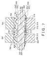
Fig. 7 shows an exemplary cross section of a package in a mounting operation performed by the mountingdevice 600. Aconductive section 702 of thesubstrate 202 has a conductive property, and electrically connects thesubstrate 202 to the other electronic components or the like. Anelectronic component 704 may be an example of the first mounting target and the second mounting target. Theelectronic component 704 operates by being bonded to thesubstrate 202. Theelectronic component 704 may include aconductive section 706 to allow electric connection of theelectronic component 704 to thesubstrate 202 or the like. -
Fig. 7 shows a state, in a mounting operation performed using the mountingdevice 600, after a step of preparing thesubstrate 202 and a plurality ofelectronic components 704, a step of adjusting the relative positional relation between thesubstrate 202 and the plurality ofelectronic components 704, and a step of arranging thesubstrate 202, an anisotropicconductive film 220, and the plurality ofelectronic components 704, in the stated order. -
Fig. 8 shows an exemplary cross section of a package in a mounting operation performed by the mountingdevice 600. Specifically,Fig. 8 shows a step of sandwiching thesubstrate 202 and the plurality ofelectronic components 704, between thelower pressurizing section 102 and theupper pressurizing section 602, to pressurize them. Thepackage 800 completes after being subjected to pressure and heating, between thelower pressurizing section 102 containing thedilatancy fluid 116 and theupper pressurizing section 602 containing thedilatancy fluid 604. -
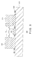
Fig. 9 shows an exemplary cross section of apackage 300 according to Embodiment Example 1. Thepackage 300 was created by mounting asubstrate 202, and first, second, and thirdelectronic components substrate 202. As each of the firstelectronic component 206 and the thirdelectronic component 214, a dummy element made of the heat resistant glass base epoxy resin laminate and having a surface area of 3*2mm2 and a height of 1.35mm was prepared. As the secondelectronic component 210, a 1005-size 0Ω jumper resistor having a height of 0.35mm was prepared. The width of the secondelectronic component 210 is 0.5mm. ACF was prepared as the anisotropicconductive film 220. - Here, the
dilatancy fluid 116 is sand, and thebase 118 is a sand-filled base. The sand-filled base filled with sand is used as alower pressurizing section 102. The average particle diameter of sand in the sand-filled base is 0.25mm. A metal head was used as anupper pressurizing section 104. - The relative positional relation among the heat resistant glass base epoxy resin laminate, the dummy elements, and the 0Ω jumper resistor is adjusted, and the heat resistant glass base epoxy resin laminate, the ACF, the dummy elements, and the 0Ω jumper resistor were arranged in the stated order. The heat resistant glass base epoxy resin laminate, the dummy elements, and the 0Ω jumper resistor were sandwiched between the sand-filled base and the metal head, and were subjected to thermocompression bonding for 20 seconds at a temperature of 180 degrees centigrade and at a pressure of 2MPa, thereby completing the
package 300. As Comparison Example 1, a package was created by using a ceramic base as alower pressurizing section 102 and an elastic member as anupper pressurizing section 104, which were subjected to thermo compression bonding under the same condition as Embodiment Example 1. - The conduction contact resistance of the 0Ω jumper resistor was evaluated in cases where the height difference between the dummy elements and the 0Ω jumper resistor is adjusted to 1.0mm and to 1.5mm, respectively. The height difference H between the dummy elements and the 0Ω jumper resistor is shown by the arrow H in
Fig. 9 . -
Table 1 HEIGHT DIFFERENCE (H) (mm) INTERELEMENT SPACING (D1) (mm) INTERELEMENT SPACING (D2) (mm) EMBODIMENT EXAMPLE 1 COMPARISON EXAMPLE 1 1.0 0.9 0.2 ○ × 1.1 0.3 ○ × 1.3 0.4 ○ ○ 1.5 0.9 0.2 ○ × 1.1 0.3 ○ × 1.3 0.4 ○ × 1.5 0.5 ○ ○ - Table 1 shows the result of evaluating the conduction contact resistance for the
package 300 of Embodiment Example 1 and the package of Comparison Example 1. ○ in Table 1 indicates that the conduction contact resistance is evaluated as 0.2Ω or be low so that conduction is possible, and × indicates that the conduction contact resistance is evaluated to exceed 0.2Ω so that conduction is impossible. - When the height difference H between the dummy elements (i.e. first and third
electronic components 206 and 214) and the 0Ω jumper resistor (i.e. second electronic component 210) is adjusted to be 1.0mm, the conduction is not possible in Comparison Example 1 unless the spacing D1 between the dummy elements is 1.3mm or greater, which corresponds to the spacing of 0.4mm between the dummy elements and the 0Ω jumper resistor. In contrast, in Embodiment Example 1, the conduction was still possible even when the spacing D1 between the dummy elements was narrowed down to 0.9mm, which corresponds to the spacing of 0.2mm between the dummy elements and the 0Ω jumper resistor. In Comparison Example 1, when the height difference H between the dummy elements and the 0Ω jumper resistor is 1.5mm, the conduction is not possible unless the spacing D1 between the dummy elements is 1.5mm or greater, which corresponds to the spacing of 0.5mm between the dummy elements and the 0Ω jumper resistor. In contrast, in Embodiment Example 1, the conduction was still allowed even when the spacing D1 between the dummy elements was narrowed down to 0.9mm, which corresponds to the spacing of 0.2mm between the dummy elements and the 0Ω jumper resistor. The evaluation results in Table 1 show that the technique of the present embodiment enables to prevent failure in mounting the components to a package. - As a
substrate 202, prepared is a TEG (test element group) substrate having lamination of heat resistant glass base epoxy resins and being provided with conductive sections at 200 µm pitch. A resistor of 1005-size is bonded to the lower surface of thesubstrate 202. A flexible print circuit provided with conductive sections at 200 µm pitch is prepared as aflexible print circuit 404. - Toluene was added to a 30 mass portion of Phenoxy resin (PKHH, manufactured by Union Carbide Corporation), a 10 mass portion of liquid epoxy resin (EP828, manufactured by Japan Epoxy Resins Co., Ltd.), a 1 mass portion of silane coupling agent (A-187, manufactured by Momentive Performance Materials Inc.), a 10 mass portion of rubber component (SG80H, manufactured by Nagase Chemtech Corp.), a 9 mass portion of conductive particles (Ni-Au plating ϕ5 µm, manufactured by Sony Chemical & Information Device Corporation), and a 40 mass portion of a hardening agent (HX3941HP, manufactured by Asahi Kasei Chemicals Corporation). The result was then adjusted to a resin solution having 50% solid content, and was applied to release PET film (manufactured by Sony Chemical & Information Device Corporation) using a bar coater. Then the solvent was dried in an oven at a temperature of 80 degrees centigrade, thereby preparing an anisotropic
conductive film 220 having a thickness of 20 µm. - Sand was used as a
dilatancy fluid 116, and a sand-filled base was used as abase 118. The sand-filled base filled with sand was used as alow pressures section 102. The average particle diameter of sand in the sand-filled base was 0.25mm. A metal head was used as anupper pressurizing section 104. - The relative positional relation among the TEG substrate and the flexible print circuit was adjusted, and the TEG substrate, the anisotropic
conductive film 220, and the flexible print circuit were arranged in the stated order. The TEG substrate and the flexible print circuit were sandwiched between the sand-filled base and the metal head, and were subjected to thermocompression bonding for 10 seconds at a temperature of 190 degrees centigrade and at a pressure of 3MPa, thereby completing thepackage 500. As Comparison Example 2, a package was created by using a rubber base as alower pressurizing section 102, and a metal head as anupper pressurizing section 104, which were subjected to thermocompression bonding under the same condition as Embodiment Example 2. As Comparison Example 3, a package was created by using an excavated base as alower pressurizing section 102, and a metal head as anupper pressurizing section 104, which were subjected to thermocompression bonding under the same condition as Embodiment Example 2, where the excavated base has convex and concave in accordance with the form of a 1005R-size resistor bonded to the lower surface of thesubstrate 202. As Comparison Example 4, a package was created by thermocompression bonding a flexible print circuit to a TEG substrate having no electronic component bonded to the lower surface thereof. - Under the high-temperature and high-humidity condition (i.e. temperature of 85 degrees centigrade and 85%RH humidity), 1000hr aging test was conducted, to evaluate the conduction resistance between the substrate and the flexible print circuit of the package, for Embodiment Example 2, Comparison Example 2, Comparison Example 3, and Comparison example 4. The evaluation of the conduction resistance was performed using a four probe method.
-
Fig. 10 shows the evaluation result for Embodiment Example 2, Comparison Example 2, Comparison Example 3, and Comparison Example 4. For Comparison Example 2 and Comparison Example 3, in the lapse of aging time, the conduction resistance increased. In other words, the electric connection was instable in the package according to Comparison Example 2 and Comparison Example 3. On the other hand, Embodiment Example 2 was able to restrain conduction resistance increase in the lapse of aging time, just as Comparison Example 4. The evaluation result of Embodiment Example 2 indicates that the technique of the present embodiment enables to stabilize electric connection of a package. - The mounting
device 100 and the mountingdevice 600 used in the above-described embodiments are of so-called face-down type. However, the mountingdevice 100 and the mountingdevice 600 are not limited to the face-down type, and can adopt a face-up type where pressurizing is conducted in a state where a plurality of electronic apparatuses are provided on an upper side of asubstrate 202. The present invention can also adopt such a type of mounting device that pressurizes a substrate in a vertically upright state between alower pressurizing section 102 and anupper pressurizing section 104 facing each other in the horizontal direction. - Although some aspects of the present invention have been described by way of exemplary embodiments, it should be understood that those skilled in the art might make many changes and substitutions without departing from the spirit and the scope of the present invention which is defined only by the appended claims.
The operations, the processes, the steps, or the like in the apparatus, the system, the program, and the method described in the claims, the specification, and the drawings are not necessarily performed in the described order. The operations, the processes, the steps, or the like can be performed in an arbitrary order, unless the output of the former-described processing is used in the later processing. Even when expressions such as "First," or "Next," or the like are used to explain the operational flow in the claims, the specification, or the drawings, they are intended to facilitate the understanding of the invention, and are never intended to show that the described order is mandatory. -
-
Fig. 1 shows an overview of a mountingdevice 100 according to the present embodiment. -
Fig. 2 shows an exemplary cross section of apackage 300 in a mounting operation. -
Fig. 3 shows an exemplary cross section of thepackage 300 in a mounting operation. -
Fig. 4 shows an exemplary cross section of apackage 500 in a mounting operation. -
Figs. 5 shows an exemplary cross section of thepackage 500 in a mounting operation. -
Fig. 6 shows an overview of a mountingdevice 600 according to a modification example of the present embodiment. -
Fig. 7 shows an exemplary cross section of apackage 800 in a mounting operation. -
Fig. 8 shows an exemplary cross section of thepackage 800 in a mounting operation. -
Fig. 9 shows an exemplary cross section of apackage 300 according to Embodiment Example 1. -
Fig. 10 shows an evaluation result of Embodiment Example 2.
Claims (11)
- A mounting device comprising:a first pressurizing section and a second pressurizing section which are used in performing mounting, whereinthe first pressurizing section or the second pressurizing section includes a dilatancy fluid.
- The mounting device according to Claim 1, wherein
the first pressurizing section or the second pressurizing section includes a heating section. - The mounting device according to Claim 1 or Claim 2, wherein
pressurizing surfaces respectively of the first pressurizing section and the second pressurizing section are substantially flat,
the first pressurizing section includes the dilatancy fluid, and
the second pressurizing section is provided above the first pressurizing section. - The mounting device according to Claim 3, further comprising:a cover sheet that covers an upper surface of the dilatancy fluid;a carrier that carries the cover sheet; anda leveling section provided to an end of the first pressurizing section, the leveling section restraining the dilatancy fluid from being carried away with the cover sheet, whereinthe first pressurizing section and the second pressurizing section perform the mounting via the cover sheet.
- The mounting device according to any of Claims 1 - 4, wherein
the first pressurizing section and the second pressurizing section pressurize a first mounting target and a second mounting target sandwiched between the first pressurizing section and the second pressurizing section. - A mounting method, comprising:adjusting a relative positional relation between a first mounting target and a second mounting target; andsandwiching and pressurizing the first mounting target and the second mounting target between a first pressurizing section and a second pressurizing section, whereinthe first pressurizing section or the second pressurizing section includes a dilatancy fluid.
- The mounting method according to Claim 6, prior to adjusting the relative positional relation, further comprising:arranging the first mounting target, an anisotropic conductive film, and the second mounting target, in the stated order.
- A package comprising a first electronic component and a second electronic component, the package obtained by a) adjusting a relative positional relation between the first electronic component and the second electronic component, and b) sandwiching and pressurizing the first electronic component and the second electronic component between a first pressurizing section and a second pressurizing section, wherein
at least one of the first pressurizing section and the second pressurizing section includes a dilatancy fluid. - A package comprising a first electronic component, an anisotropic conductive film, and a second electronic component, the package obtained by a) adjusting a relative positional relation between the first electronic component and the second electronic component, b) arranging the first electronic component, the anisotropic conductive film, and the second electronic component in the stated order, and c) sandwiching and pressurizing the first electronic component and the second electronic component between a first pressurizing section and a second pressurizing section, wherein
at least one of the first pressurizing section and the second pressurizing section includes a dilatancy fluid. - A package comprising:a substrate and a plurality of electronic components mounted to the substrate, whereinthe plurality of electronic components are a first electronic component, a second electronic component, and a third electronic component arranged in the stated order in a direction substantially parallel to a main surface of the substrate,in a direction substantially vertical to the main surface of the substrate, a maximum distance between the first and the third electronic components and the second electronic component is 1mm or above, andin a direction substantially parallel to the main surface of the substrate, a minimum distance between the first electronic component and the third electronic component is 0.8mm or below.
- A pressurizing plate for use in a pressurizing apparatus for mounting and electrically coupling a plurality of electric components, the pressurizing plate comprising:a dilatancy fluid; anda base that retains the dilatancy fluid.
Applications Claiming Priority (3)
| Application Number | Priority Date | Filing Date | Title |
|---|---|---|---|
| JP2008206217 | 2008-08-08 | ||
| JP2008242946A JP4916494B2 (en) | 2008-08-08 | 2008-09-22 | Crimping apparatus, crimping method, and pressing plate |
| PCT/JP2009/001901 WO2010016170A1 (en) | 2008-08-08 | 2009-04-24 | Compression bonding device, compression bonding method, package, and pressing plate |
Publications (3)
| Publication Number | Publication Date |
|---|---|
| EP2309834A1 true EP2309834A1 (en) | 2011-04-13 |
| EP2309834A4 EP2309834A4 (en) | 2011-09-14 |
| EP2309834B1 EP2309834B1 (en) | 2015-02-25 |
Family
ID=41663399
Family Applications (1)
| Application Number | Title | Priority Date | Filing Date |
|---|---|---|---|
| EP09804657.6A Not-in-force EP2309834B1 (en) | 2008-08-08 | 2009-04-24 | Compression bonding device, compression bonding method and pressing plate |
Country Status (7)
| Country | Link |
|---|---|
| US (1) | US8296939B2 (en) |
| EP (1) | EP2309834B1 (en) |
| JP (1) | JP4916494B2 (en) |
| KR (1) | KR20110039510A (en) |
| CN (1) | CN101810067B (en) |
| TW (1) | TWI436700B (en) |
| WO (1) | WO2010016170A1 (en) |
Families Citing this family (7)
| Publication number | Priority date | Publication date | Assignee | Title |
|---|---|---|---|---|
| JP2011109046A (en) * | 2009-11-20 | 2011-06-02 | Sony Chemical & Information Device Corp | Mounting apparatus and method for manufacturing electronic module |
| JP6041463B2 (en) * | 2009-12-25 | 2016-12-07 | デクセリアルズ株式会社 | Epoxy resin composition, method for producing joined body using the same, and joined body |
| DE102010039749A1 (en) * | 2010-08-25 | 2012-03-01 | Robert Bosch Gmbh | A method of assembling a multi-component circuit board and an electrical circuit comprising a circuit board and a plurality of components mounted thereon |
| WO2016068165A1 (en) * | 2014-10-29 | 2016-05-06 | デクセリアルズ株式会社 | Conductive material |
| TWI581942B (en) * | 2015-04-08 | 2017-05-11 | 韋僑科技股份有限公司 | Crimping apparatus and system and method for crimping a flexible printed circuit using the same |
| TWI681701B (en) * | 2018-09-03 | 2020-01-01 | 活躍科技股份有限公司 | Energy-saving platen press |
| CN109335675B (en) * | 2018-11-09 | 2024-07-05 | 南京富信节能科技有限公司 | Automatic ball top sticking machine and working method thereof |
Family Cites Families (16)
| Publication number | Priority date | Publication date | Assignee | Title |
|---|---|---|---|---|
| US3529117A (en) * | 1969-09-11 | 1970-09-15 | Argus Eng Co | Soldering apparatus |
| JPH0690099A (en) * | 1992-06-09 | 1994-03-29 | Ibiden Co Ltd | Jig for supporting substrate |
| US5414298A (en) * | 1993-03-26 | 1995-05-09 | Tessera, Inc. | Semiconductor chip assemblies and components with pressure contact |
| JPH08146451A (en) * | 1994-11-16 | 1996-06-07 | Sony Corp | Circuit device manufacturing equipment |
| JPH10150297A (en) * | 1996-11-18 | 1998-06-02 | Toyo Commun Equip Co Ltd | Support jig for mounting electronic components |
| JP2002017519A (en) * | 2000-07-06 | 2002-01-22 | Toyo Tire & Rubber Co Ltd | Equalizing mat |
| JP2004322490A (en) * | 2003-04-25 | 2004-11-18 | Konica Minolta Photo Imaging Inc | Laminated body manufacturing method and laminated body manufacturing apparatus |
| JP3921459B2 (en) * | 2003-07-11 | 2007-05-30 | ソニーケミカル&インフォメーションデバイス株式会社 | Mounting method and mounting apparatus for electrical parts |
| JP4274126B2 (en) * | 2005-01-18 | 2009-06-03 | パナソニック株式会社 | Crimping apparatus and crimping method |
| EP1845556A4 (en) * | 2005-02-02 | 2010-02-10 | Sony Chem & Inf Device Corp | APPARATUS FOR MOUNTING ELECTRICAL COMPONENTS |
| CN1307699C (en) * | 2005-03-14 | 2007-03-28 | 西安交通大学 | Method for making crimping interconnection technology based power electronic integrated module |
| JP4925669B2 (en) | 2006-01-13 | 2012-05-09 | ソニーケミカル&インフォメーションデバイス株式会社 | Crimping apparatus and mounting method |
| JP4832107B2 (en) | 2006-02-23 | 2011-12-07 | ソニーケミカル&インフォメーションデバイス株式会社 | Implementation method |
| JP2007294607A (en) * | 2006-04-24 | 2007-11-08 | Sony Chemical & Information Device Corp | Press head and press device |
| JP2008206217A (en) | 2007-02-16 | 2008-09-04 | Yaskawa Electric Corp | Semiconductor power conversion device having life monitoring circuit of semiconductor switching element |
| JP2008242946A (en) | 2007-03-28 | 2008-10-09 | Toshiba Corp | Electronic device and key press determination method |
-
2008
- 2008-09-22 JP JP2008242946A patent/JP4916494B2/en not_active Expired - Fee Related
-
2009
- 2009-04-24 CN CN2009800004033A patent/CN101810067B/en not_active Expired - Fee Related
- 2009-04-24 KR KR1020097025760A patent/KR20110039510A/en not_active Ceased
- 2009-04-24 EP EP09804657.6A patent/EP2309834B1/en not_active Not-in-force
- 2009-04-24 WO PCT/JP2009/001901 patent/WO2010016170A1/en not_active Ceased
- 2009-06-11 TW TW098119562A patent/TWI436700B/en not_active IP Right Cessation
- 2009-12-10 US US12/635,651 patent/US8296939B2/en not_active Expired - Fee Related
Also Published As
| Publication number | Publication date |
|---|---|
| US8296939B2 (en) | 2012-10-30 |
| CN101810067A (en) | 2010-08-18 |
| KR20110039510A (en) | 2011-04-19 |
| EP2309834B1 (en) | 2015-02-25 |
| JP4916494B2 (en) | 2012-04-11 |
| TWI436700B (en) | 2014-05-01 |
| CN101810067B (en) | 2013-07-10 |
| HK1143023A1 (en) | 2010-12-17 |
| WO2010016170A1 (en) | 2010-02-11 |
| TW201018329A (en) | 2010-05-01 |
| EP2309834A4 (en) | 2011-09-14 |
| US20100085723A1 (en) | 2010-04-08 |
| JP2010062504A (en) | 2010-03-18 |
Similar Documents
| Publication | Publication Date | Title |
|---|---|---|
| EP2309834B1 (en) | Compression bonding device, compression bonding method and pressing plate | |
| Lin et al. | A review of the influencing factors on anisotropic conductive adhesives joining technology in electrical applications | |
| KR101193735B1 (en) | Adhesive film, connection method, and assembly | |
| KR101376002B1 (en) | Adhesive composition, circuit connecting material using the same, method for connecting circuit members, and circuit connection structure | |
| KR101398307B1 (en) | Method and apparatus for mounting electric parts | |
| JP3801666B2 (en) | Electrode connection method and connection member used therefor | |
| KR20160114054A (en) | Connection body and connection body production method | |
| US20120222808A1 (en) | Mounting device and method for manufacturing electronic module | |
| KR102028384B1 (en) | Connection device, method for manufacturing connection structure, method for manufacturing stacked chip component and method for mounting electronic component | |
| CN101889335B (en) | Method and apparatus for mounting electric component | |
| WO2006056999A2 (en) | Methods for manufacturing a sensor assembly | |
| KR102028466B1 (en) | Method for manufacturing connecting body, and method for connecting electronic component | |
| JP4378788B2 (en) | IC chip connection method | |
| CN107230646B (en) | Method for making linker | |
| KR102758192B1 (en) | Adhesive composition | |
| Ramkumar et al. | Novel anisotropic conductive adhesive for 3D stacking and lead-free PCB packaging—A review | |
| JP2011081257A (en) | Method for manufacturing circuit component | |
| JP2010166097A (en) | Connection method and connection structure obtained by using connection apparatus and the connection method | |
| HK1143023B (en) | Compression bonding device, compression bonding method, package and pressurizing plate | |
| KR20220161358A (en) | Adhesive composition and bonded structure | |
| JP6431572B2 (en) | Connection film, connection film manufacturing method, connection structure, connection structure manufacturing method, and connection method | |
| JP2003060333A (en) | How to connect electronic components | |
| JP6177642B2 (en) | Connection film, connection structure, method for manufacturing connection structure, connection method | |
| Ramkumar et al. | Influence of Filler Modifications on the Performance of a Novel Anisotropic Conductive Adhesive under Temperature/Humidity Aging | |
| HK1225165B (en) | Electronic component, connector, connector production method, and electronic component connecting method |
Legal Events
| Date | Code | Title | Description |
|---|---|---|---|
| PUAI | Public reference made under article 153(3) epc to a published international application that has entered the european phase |
Free format text: ORIGINAL CODE: 0009012 |
|
| 17P | Request for examination filed |
Effective date: 20100330 |
|
| AK | Designated contracting states |
Kind code of ref document: A1 Designated state(s): AT BE BG CH CY CZ DE DK EE ES FI FR GB GR HR HU IE IS IT LI LT LU LV MC MK MT NL NO PL PT RO SE SI SK TR |
|
| AX | Request for extension of the european patent |
Extension state: AL BA RS |
|
| A4 | Supplementary search report drawn up and despatched |
Effective date: 20110816 |
|
| RIC1 | Information provided on ipc code assigned before grant |
Ipc: H01L 21/60 20060101ALI20110809BHEP Ipc: H05K 13/04 20060101AFI20110809BHEP Ipc: H05K 3/32 20060101ALI20110809BHEP |
|
| DAX | Request for extension of the european patent (deleted) | ||
| RAP1 | Party data changed (applicant data changed or rights of an application transferred) |
Owner name: DEXERIALS CORPORATION |
|
| 17Q | First examination report despatched |
Effective date: 20140416 |
|
| GRAP | Despatch of communication of intention to grant a patent |
Free format text: ORIGINAL CODE: EPIDOSNIGR1 |
|
| INTG | Intention to grant announced |
Effective date: 20140922 |
|
| GRAS | Grant fee paid |
Free format text: ORIGINAL CODE: EPIDOSNIGR3 |
|
| GRAA | (expected) grant |
Free format text: ORIGINAL CODE: 0009210 |
|
| AK | Designated contracting states |
Kind code of ref document: B1 Designated state(s): AT BE BG CH CY CZ DE DK EE ES FI FR GB GR HR HU IE IS IT LI LT LU LV MC MK MT NL NO PL PT RO SE SI SK TR |
|
| REG | Reference to a national code |
Ref country code: GB Ref legal event code: FG4D |
|
| REG | Reference to a national code |
Ref country code: CH Ref legal event code: EP |
|
| REG | Reference to a national code |
Ref country code: IE Ref legal event code: FG4D |
|
| REG | Reference to a national code |
Ref country code: DE Ref legal event code: R096 Ref document number: 602009029653 Country of ref document: DE Effective date: 20150409 |
|
| REG | Reference to a national code |
Ref country code: AT Ref legal event code: REF Ref document number: 712945 Country of ref document: AT Kind code of ref document: T Effective date: 20150415 |
|
| REG | Reference to a national code |
Ref country code: NL Ref legal event code: T3 |
|
| REG | Reference to a national code |
Ref country code: AT Ref legal event code: MK05 Ref document number: 712945 Country of ref document: AT Kind code of ref document: T Effective date: 20150225 |
|
| REG | Reference to a national code |
Ref country code: LT Ref legal event code: MG4D |
|
| PG25 | Lapsed in a contracting state [announced via postgrant information from national office to epo] |
Ref country code: FI Free format text: LAPSE BECAUSE OF FAILURE TO SUBMIT A TRANSLATION OF THE DESCRIPTION OR TO PAY THE FEE WITHIN THE PRESCRIBED TIME-LIMIT Effective date: 20150225 Ref country code: HR Free format text: LAPSE BECAUSE OF FAILURE TO SUBMIT A TRANSLATION OF THE DESCRIPTION OR TO PAY THE FEE WITHIN THE PRESCRIBED TIME-LIMIT Effective date: 20150225 Ref country code: ES Free format text: LAPSE BECAUSE OF FAILURE TO SUBMIT A TRANSLATION OF THE DESCRIPTION OR TO PAY THE FEE WITHIN THE PRESCRIBED TIME-LIMIT Effective date: 20150225 Ref country code: SE Free format text: LAPSE BECAUSE OF FAILURE TO SUBMIT A TRANSLATION OF THE DESCRIPTION OR TO PAY THE FEE WITHIN THE PRESCRIBED TIME-LIMIT Effective date: 20150225 Ref country code: NO Free format text: LAPSE BECAUSE OF FAILURE TO SUBMIT A TRANSLATION OF THE DESCRIPTION OR TO PAY THE FEE WITHIN THE PRESCRIBED TIME-LIMIT Effective date: 20150525 Ref country code: LT Free format text: LAPSE BECAUSE OF FAILURE TO SUBMIT A TRANSLATION OF THE DESCRIPTION OR TO PAY THE FEE WITHIN THE PRESCRIBED TIME-LIMIT Effective date: 20150225 |
|
| PG25 | Lapsed in a contracting state [announced via postgrant information from national office to epo] |
Ref country code: IS Free format text: LAPSE BECAUSE OF FAILURE TO SUBMIT A TRANSLATION OF THE DESCRIPTION OR TO PAY THE FEE WITHIN THE PRESCRIBED TIME-LIMIT Effective date: 20150625 Ref country code: GR Free format text: LAPSE BECAUSE OF FAILURE TO SUBMIT A TRANSLATION OF THE DESCRIPTION OR TO PAY THE FEE WITHIN THE PRESCRIBED TIME-LIMIT Effective date: 20150526 Ref country code: AT Free format text: LAPSE BECAUSE OF FAILURE TO SUBMIT A TRANSLATION OF THE DESCRIPTION OR TO PAY THE FEE WITHIN THE PRESCRIBED TIME-LIMIT Effective date: 20150225 Ref country code: LV Free format text: LAPSE BECAUSE OF FAILURE TO SUBMIT A TRANSLATION OF THE DESCRIPTION OR TO PAY THE FEE WITHIN THE PRESCRIBED TIME-LIMIT Effective date: 20150225 |
|
| PG25 | Lapsed in a contracting state [announced via postgrant information from national office to epo] |
Ref country code: CZ Free format text: LAPSE BECAUSE OF FAILURE TO SUBMIT A TRANSLATION OF THE DESCRIPTION OR TO PAY THE FEE WITHIN THE PRESCRIBED TIME-LIMIT Effective date: 20150225 Ref country code: EE Free format text: LAPSE BECAUSE OF FAILURE TO SUBMIT A TRANSLATION OF THE DESCRIPTION OR TO PAY THE FEE WITHIN THE PRESCRIBED TIME-LIMIT Effective date: 20150225 Ref country code: DK Free format text: LAPSE BECAUSE OF FAILURE TO SUBMIT A TRANSLATION OF THE DESCRIPTION OR TO PAY THE FEE WITHIN THE PRESCRIBED TIME-LIMIT Effective date: 20150225 Ref country code: SK Free format text: LAPSE BECAUSE OF FAILURE TO SUBMIT A TRANSLATION OF THE DESCRIPTION OR TO PAY THE FEE WITHIN THE PRESCRIBED TIME-LIMIT Effective date: 20150225 Ref country code: RO Free format text: LAPSE BECAUSE OF FAILURE TO SUBMIT A TRANSLATION OF THE DESCRIPTION OR TO PAY THE FEE WITHIN THE PRESCRIBED TIME-LIMIT Effective date: 20150225 |
|
| REG | Reference to a national code |
Ref country code: DE Ref legal event code: R097 Ref document number: 602009029653 Country of ref document: DE |
|
| PG25 | Lapsed in a contracting state [announced via postgrant information from national office to epo] |
Ref country code: LU Free format text: LAPSE BECAUSE OF FAILURE TO SUBMIT A TRANSLATION OF THE DESCRIPTION OR TO PAY THE FEE WITHIN THE PRESCRIBED TIME-LIMIT Effective date: 20150424 Ref country code: MC Free format text: LAPSE BECAUSE OF FAILURE TO SUBMIT A TRANSLATION OF THE DESCRIPTION OR TO PAY THE FEE WITHIN THE PRESCRIBED TIME-LIMIT Effective date: 20150225 Ref country code: PL Free format text: LAPSE BECAUSE OF FAILURE TO SUBMIT A TRANSLATION OF THE DESCRIPTION OR TO PAY THE FEE WITHIN THE PRESCRIBED TIME-LIMIT Effective date: 20150225 |
|
| REG | Reference to a national code |
Ref country code: CH Ref legal event code: PL |
|
| PLBE | No opposition filed within time limit |
Free format text: ORIGINAL CODE: 0009261 |
|
| STAA | Information on the status of an ep patent application or granted ep patent |
Free format text: STATUS: NO OPPOSITION FILED WITHIN TIME LIMIT |
|
| REG | Reference to a national code |
Ref country code: IE Ref legal event code: MM4A |
|
| PG25 | Lapsed in a contracting state [announced via postgrant information from national office to epo] |
Ref country code: CH Free format text: LAPSE BECAUSE OF NON-PAYMENT OF DUE FEES Effective date: 20150430 Ref country code: LI Free format text: LAPSE BECAUSE OF NON-PAYMENT OF DUE FEES Effective date: 20150430 |
|
| 26N | No opposition filed |
Effective date: 20151126 |
|
| PG25 | Lapsed in a contracting state [announced via postgrant information from national office to epo] |
Ref country code: SI Free format text: LAPSE BECAUSE OF FAILURE TO SUBMIT A TRANSLATION OF THE DESCRIPTION OR TO PAY THE FEE WITHIN THE PRESCRIBED TIME-LIMIT Effective date: 20150225 |
|
| REG | Reference to a national code |
Ref country code: FR Ref legal event code: PLFP Year of fee payment: 8 |
|
| PG25 | Lapsed in a contracting state [announced via postgrant information from national office to epo] |
Ref country code: IE Free format text: LAPSE BECAUSE OF NON-PAYMENT OF DUE FEES Effective date: 20150424 |
|
| PGFP | Annual fee paid to national office [announced via postgrant information from national office to epo] |
Ref country code: NL Payment date: 20160310 Year of fee payment: 8 |
|
| PG25 | Lapsed in a contracting state [announced via postgrant information from national office to epo] |
Ref country code: BE Free format text: LAPSE BECAUSE OF FAILURE TO SUBMIT A TRANSLATION OF THE DESCRIPTION OR TO PAY THE FEE WITHIN THE PRESCRIBED TIME-LIMIT Effective date: 20150225 |
|
| PGFP | Annual fee paid to national office [announced via postgrant information from national office to epo] |
Ref country code: FR Payment date: 20160309 Year of fee payment: 8 |
|
| PGFP | Annual fee paid to national office [announced via postgrant information from national office to epo] |
Ref country code: DE Payment date: 20160419 Year of fee payment: 8 Ref country code: GB Payment date: 20160420 Year of fee payment: 8 |
|
| PGFP | Annual fee paid to national office [announced via postgrant information from national office to epo] |
Ref country code: IT Payment date: 20160418 Year of fee payment: 8 |
|
| PG25 | Lapsed in a contracting state [announced via postgrant information from national office to epo] |
Ref country code: MT Free format text: LAPSE BECAUSE OF FAILURE TO SUBMIT A TRANSLATION OF THE DESCRIPTION OR TO PAY THE FEE WITHIN THE PRESCRIBED TIME-LIMIT Effective date: 20150225 |
|
| PG25 | Lapsed in a contracting state [announced via postgrant information from national office to epo] |
Ref country code: HU Free format text: LAPSE BECAUSE OF FAILURE TO SUBMIT A TRANSLATION OF THE DESCRIPTION OR TO PAY THE FEE WITHIN THE PRESCRIBED TIME-LIMIT; INVALID AB INITIO Effective date: 20090424 Ref country code: BG Free format text: LAPSE BECAUSE OF FAILURE TO SUBMIT A TRANSLATION OF THE DESCRIPTION OR TO PAY THE FEE WITHIN THE PRESCRIBED TIME-LIMIT Effective date: 20150225 |
|
| PG25 | Lapsed in a contracting state [announced via postgrant information from national office to epo] |
Ref country code: CY Free format text: LAPSE BECAUSE OF FAILURE TO SUBMIT A TRANSLATION OF THE DESCRIPTION OR TO PAY THE FEE WITHIN THE PRESCRIBED TIME-LIMIT Effective date: 20150225 |
|
| PG25 | Lapsed in a contracting state [announced via postgrant information from national office to epo] |
Ref country code: PT Free format text: LAPSE BECAUSE OF FAILURE TO SUBMIT A TRANSLATION OF THE DESCRIPTION OR TO PAY THE FEE WITHIN THE PRESCRIBED TIME-LIMIT Effective date: 20150625 |
|
| PG25 | Lapsed in a contracting state [announced via postgrant information from national office to epo] |
Ref country code: TR Free format text: LAPSE BECAUSE OF FAILURE TO SUBMIT A TRANSLATION OF THE DESCRIPTION OR TO PAY THE FEE WITHIN THE PRESCRIBED TIME-LIMIT Effective date: 20150225 |
|
| REG | Reference to a national code |
Ref country code: DE Ref legal event code: R119 Ref document number: 602009029653 Country of ref document: DE |
|
| REG | Reference to a national code |
Ref country code: NL Ref legal event code: MM Effective date: 20170501 |
|
| GBPC | Gb: european patent ceased through non-payment of renewal fee |
Effective date: 20170424 |
|
| REG | Reference to a national code |
Ref country code: FR Ref legal event code: ST Effective date: 20171229 |
|
| PG25 | Lapsed in a contracting state [announced via postgrant information from national office to epo] |
Ref country code: NL Free format text: LAPSE BECAUSE OF NON-PAYMENT OF DUE FEES Effective date: 20170501 Ref country code: DE Free format text: LAPSE BECAUSE OF NON-PAYMENT OF DUE FEES Effective date: 20171103 Ref country code: FR Free format text: LAPSE BECAUSE OF NON-PAYMENT OF DUE FEES Effective date: 20170502 |
|
| PG25 | Lapsed in a contracting state [announced via postgrant information from national office to epo] |
Ref country code: GB Free format text: LAPSE BECAUSE OF NON-PAYMENT OF DUE FEES Effective date: 20170424 |
|
| PG25 | Lapsed in a contracting state [announced via postgrant information from national office to epo] |
Ref country code: IT Free format text: LAPSE BECAUSE OF NON-PAYMENT OF DUE FEES Effective date: 20170424 |
|
| PG25 | Lapsed in a contracting state [announced via postgrant information from national office to epo] |
Ref country code: MK Free format text: LAPSE BECAUSE OF FAILURE TO SUBMIT A TRANSLATION OF THE DESCRIPTION OR TO PAY THE FEE WITHIN THE PRESCRIBED TIME-LIMIT Effective date: 20150225 |