EP2309541A2 - Solid-state image sensor and image sensing apparatus - Google Patents
Solid-state image sensor and image sensing apparatus Download PDFInfo
- Publication number
- EP2309541A2 EP2309541A2 EP10177869A EP10177869A EP2309541A2 EP 2309541 A2 EP2309541 A2 EP 2309541A2 EP 10177869 A EP10177869 A EP 10177869A EP 10177869 A EP10177869 A EP 10177869A EP 2309541 A2 EP2309541 A2 EP 2309541A2
- Authority
- EP
- European Patent Office
- Prior art keywords
- pixel
- group
- readout line
- column readout
- column
- Prior art date
- Legal status (The legal status is an assumption and is not a legal conclusion. Google has not performed a legal analysis and makes no representation as to the accuracy of the status listed.)
- Granted
Links
- 238000006243 chemical reaction Methods 0.000 claims abstract description 52
- 238000012546 transfer Methods 0.000 claims description 23
- 230000003321 amplification Effects 0.000 claims description 14
- 238000003199 nucleic acid amplification method Methods 0.000 claims description 14
- 238000012545 processing Methods 0.000 claims description 13
- 239000003086 colorant Substances 0.000 claims description 4
- 238000000034 method Methods 0.000 claims description 4
- 230000008569 process Effects 0.000 claims description 3
- 230000000295 complement effect Effects 0.000 claims description 2
- 238000010586 diagram Methods 0.000 description 17
- 230000008878 coupling Effects 0.000 description 5
- 238000010168 coupling process Methods 0.000 description 5
- 238000005859 coupling reaction Methods 0.000 description 5
- 238000003491 array Methods 0.000 description 4
- 239000000470 constituent Substances 0.000 description 4
- 238000012937 correction Methods 0.000 description 3
- 230000004888 barrier function Effects 0.000 description 2
- 238000013461 design Methods 0.000 description 2
- 238000004519 manufacturing process Methods 0.000 description 2
- 230000004048 modification Effects 0.000 description 2
- 238000012986 modification Methods 0.000 description 2
- 230000003071 parasitic effect Effects 0.000 description 2
- 230000003213 activating effect Effects 0.000 description 1
- 230000008859 change Effects 0.000 description 1
- 238000004891 communication Methods 0.000 description 1
- 238000013144 data compression Methods 0.000 description 1
- 238000009792 diffusion process Methods 0.000 description 1
- 239000000284 extract Substances 0.000 description 1
- 230000006870 function Effects 0.000 description 1
- 230000007246 mechanism Effects 0.000 description 1
- 230000003287 optical effect Effects 0.000 description 1
- 230000001012 protector Effects 0.000 description 1
- 230000004044 response Effects 0.000 description 1
- 239000004065 semiconductor Substances 0.000 description 1
Images




Classifications
-
- H—ELECTRICITY
- H10—SEMICONDUCTOR DEVICES; ELECTRIC SOLID-STATE DEVICES NOT OTHERWISE PROVIDED FOR
- H10F—INORGANIC SEMICONDUCTOR DEVICES SENSITIVE TO INFRARED RADIATION, LIGHT, ELECTROMAGNETIC RADIATION OF SHORTER WAVELENGTH OR CORPUSCULAR RADIATION
- H10F39/00—Integrated devices, or assemblies of multiple devices, comprising at least one element covered by group H10F30/00, e.g. radiation detectors comprising photodiode arrays
- H10F39/10—Integrated devices
- H10F39/12—Image sensors
- H10F39/15—Charge-coupled device [CCD] image sensors
- H10F39/151—Geometry or disposition of pixel elements, address lines or gate electrodes
-
- H—ELECTRICITY
- H04—ELECTRIC COMMUNICATION TECHNIQUE
- H04N—PICTORIAL COMMUNICATION, e.g. TELEVISION
- H04N25/00—Circuitry of solid-state image sensors [SSIS]; Control thereof
-
- H—ELECTRICITY
- H04—ELECTRIC COMMUNICATION TECHNIQUE
- H04N—PICTORIAL COMMUNICATION, e.g. TELEVISION
- H04N25/00—Circuitry of solid-state image sensors [SSIS]; Control thereof
- H04N25/60—Noise processing, e.g. detecting, correcting, reducing or removing noise
-
- H—ELECTRICITY
- H04—ELECTRIC COMMUNICATION TECHNIQUE
- H04N—PICTORIAL COMMUNICATION, e.g. TELEVISION
- H04N25/00—Circuitry of solid-state image sensors [SSIS]; Control thereof
- H04N25/70—SSIS architectures; Circuits associated therewith
- H04N25/71—Charge-coupled device [CCD] sensors; Charge-transfer registers specially adapted for CCD sensors
- H04N25/713—Transfer or readout registers; Split readout registers or multiple readout registers
-
- H—ELECTRICITY
- H10—SEMICONDUCTOR DEVICES; ELECTRIC SOLID-STATE DEVICES NOT OTHERWISE PROVIDED FOR
- H10F—INORGANIC SEMICONDUCTOR DEVICES SENSITIVE TO INFRARED RADIATION, LIGHT, ELECTROMAGNETIC RADIATION OF SHORTER WAVELENGTH OR CORPUSCULAR RADIATION
- H10F39/00—Integrated devices, or assemblies of multiple devices, comprising at least one element covered by group H10F30/00, e.g. radiation detectors comprising photodiode arrays
- H10F39/80—Constructional details of image sensors
- H10F39/802—Geometry or disposition of elements in pixels, e.g. address-lines or gate electrodes
-
- H—ELECTRICITY
- H10—SEMICONDUCTOR DEVICES; ELECTRIC SOLID-STATE DEVICES NOT OTHERWISE PROVIDED FOR
- H10F—INORGANIC SEMICONDUCTOR DEVICES SENSITIVE TO INFRARED RADIATION, LIGHT, ELECTROMAGNETIC RADIATION OF SHORTER WAVELENGTH OR CORPUSCULAR RADIATION
- H10F39/00—Integrated devices, or assemblies of multiple devices, comprising at least one element covered by group H10F30/00, e.g. radiation detectors comprising photodiode arrays
- H10F39/80—Constructional details of image sensors
- H10F39/813—Electronic components shared by multiple pixels, e.g. one amplifier shared by two pixels
Definitions
- the present invention relates to a solid-state image sensor, and an image sensing apparatus including the same.
- Japanese Patent Laid-Open No. 2005-311821 discloses a high-rate read technique for a solid-state image sensor. More specifically, Japanese Patent Laid-Open No. 2005-311821 discloses a solid-state image sensor which includes a plurality of column readout lines provided to each column in a pixel array, and can simultaneously read signals in a plurality of rows of the pixel array by simultaneously activating those rows. Japanese Patent Laid-Open No. 2005-311821 merely discloses a mechanism in which each column in a pixel array includes a plurality of column readout lines, and does not disclose any layout diagram that shows the structure of pixels.
- the present invention provides a layout advantageous in an arrangement in which a plurality of column readout lines are arranged in each pixel column which forms a pixel array.
- the present invention in its first aspect provides a solid-state image sensor as specified in claims 1 to 8.
- the present invention in its second aspect provides an image sensing apparatus as specified in claim 9.
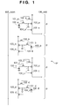
- Fig. 1 is a circuit diagram exemplifying the partial circuitry of one pixel column in a pixel array
- Fig. 2 is a plan layout diagram showing two pixel arrays in the first embodiment of the present invention.
- Fig. 3 is a plan layout diagram showing two pixel arrays in the second embodiment of the present invention.
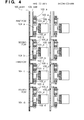
- Fig. 4 is a plan layout diagram showing two pixel arrays in the third embodiment of the present invention.
- Fig. 5 is a plan layout diagram showing two pixel arrays in the fourth embodiment of the present invention.
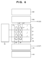
- Fig. 6 is a block diagram showing the schematic arrangement of a solid-state image sensor according to an embodiment of the present invention.
- Fig. 7 is a block diagram showing the schematic configuration of an image sensing apparatus (camera) according to an embodiment of the present invention.
- Fig. 6 is a block diagram showing the schematic arrangement of a solid-state image sensor IS according to an embodiment of the present invention.
- the solid-state image sensor IS is designed as an active pixel image sensor such as a CMOS image sensor.
- An active pixel image sensor is a solid-state image sensor in which each pixel includes a photoelectric conversion element and an amplification element which amplifies a signal obtained by photoelectric conversion by the photoelectric conversion element.
- the solid-state image sensor IS includes a pixel array PA, vertical selection circuit VS, first readout circuit HR1, second readout circuit HR2, first horizontal selection circuit HS1, and second horizontal selection circuit HS2.
- the pixel array PA includes a plurality of pixels p which are two-dimensionally arranged so as to form a plurality of pixel rows pr and a plurality of pixel columns pc.
- Each pixel p is designed as an active pixel, and includes a photoelectric conversion element and an amplification element which amplifies a signal obtained by photoelectric conversion by the photoelectric conversion element.
- Fig. 6 illustrates a pixel array simplified for the sake of descriptive convenience as the pixel array PA.
- Each pixel column pc in the pixel array PA includes two column readout lines: a first column readout line c1 and a second column readout line c2.
- the plurality of pixel rows pr which form the pixel array PA are divided into pixel rows of a first group and those of a second group.
- the first group can include odd rows (odd-numbered rows), and the second group can include even rows (even-numbered rows).
- the first group can include even rows, and the second group can include odd rows.
- the first column readout lines c1 can be used to read signals from pixels in even rows, and the second column readout lines c2 can be used to read signals from pixels in odd rows.
- the first column readout lines c1 may be used to read signals from pixels in odd rows, and the second column readout lines c2 may be used to read signals from pixels in even rows.
- an arbitrary half of the plurality of pixel rows pr which form the pixel array PA can be classified as a first group, and the remaining half can be classified as a second group.
- the vertical selection circuit VS simultaneously selects one pixel row belonging to the first group in the pixel array PA, and one pixel row belonging to the second group in the pixel array PA.
- the first readout circuit HR1 reads a signal via the first column readout line c1 from a pixel belonging to one of two simultaneously selected pixel rows pr in the pixel array PA, and outputs it to a first output terminal OUT1.
- the second readout circuit HR2 reads a signal via the second column readout line c2 from a pixel belonging to the other one of the two simultaneously selected pixel rows pr in the pixel array PA, and outputs it to a second output terminal OUT2.
- the first readout circuit HR1 and second readout circuit HR2 are preferably arranged to sandwich the pixel array PA between them.
- the first horizontal selection circuit HS1 selects a pixel column pc to be read in the pixel array PA.
- the second horizontal selection circuit HS2 also selects a pixel column pc to be read in the pixel
- Fig. 1 is a circuit diagram exemplifying the partial circuitry of one pixel column pc in the pixel array PA in the first embodiment of the present invention.
- one pixel column pc includes four pixels p in the example shown in Fig. 1 , this arrangement is illustrated by simplifying an actual arrangement for the sake of descriptive convenience. Hence, in practice, one pixel column pc can include a larger number of pixels.
- the first column readout lines c1 are assumed as column readout lines 106_even used to read signals from pixels in even rows
- the second column readout lines c2 are assumed as column readout lines 106_odd used to read signals from pixels in odd rows.
- the first column readout lines c1 may be column readout lines 106-odd used to read signals from pixels in odd rows
- the second column readout lines c2 may be column readout lines 106_even used to read signals from pixels in even rows.
- each pixel p includes a photodiode 100, a floating diffusion (to be abbreviated as an FD hereinafter) 104, an amplification transistor 103, a reset transistor 102, a row selection transistor 105, and a transfer transistor 101.
- the arrangement of each pixel p is not limited to the example shown in Fig. 1 , and the row selection transistor 105 is unnecessary in, for example, an arrangement which selects a row by controlling the voltage of the FD.
- the photodiode 100 (photodiodes 100_a, 100 b,...) exemplifies a photoelectric conversion element.
- the FD 104 (FDs 104_a, 104_b,...) exemplifies a conversion region (capacitance element) which holds a charge output from the photodiode 100 and converts it into a voltage.
- the amplification transistor 103 (amplification transistors 103_a, 103_b,...) exemplifies an amplification element which amplifies the signal transferred to the FD 104.
- the reset transistor 102 (reset transistors 102_a, 102_b,...) exemplifies a reset element which resets (initializes) the voltage of the FD 104, and can be controlled by the vertical selection circuit VS.
- the row selection transistor 105 (row selection transistors 105_a, 105_b,...) exemplifies a switch for selecting a row, and can be controlled by the vertical selection circuit VS.
- the transfer transistor 101 (transfer transistors 101_a, 101_b,...) exemplifies a transfer element for transferring a charge generated by photoelectric conversion in the photodiode 100 to the FD 104, and can be controlled by the vertical selection circuit VS.
- the reset transistors 102 in all pixels belonging to one row pr can be controlled by means of a common reset signal driven by the vertical selection circuit VS.
- the row selection transistors 105 in all pixels belonging to one row pr can be controlled by means of a common row selection signal driven by the vertical selection circuit VS.
- the transfer transistors 101 in all pixels belonging to one row Pr can be controlled by means of a common transfer signal driven by the vertical selection circuit VS.
- the vertical selection circuit VS typically simultaneously selects a pair of the first pixel row on the second pixel row, and then simultaneously selects a pair of the third pixel row on the fourth pixel row; it simultaneously selects a pair of two adjacent pixel rows. Note that when pixel rows have been selected, signals are output from pixels in the pixel rows to the column readout lines.
- a set of the above-mentioned reset signal, row selection signal, and transfer signal are shown as a control signal r in Fig. 6 .
- Fig. 2 is a plan layout diagram showing two pixel columns in a pixel array, in which each pixel column has the circuitry shown in Fig. 1 , according to the first embodiment of the present invention.
- Fig. 2 shows a pixel array including two pixels in the horizontal direction and four pixels in the vertical direction (two pixel columns x four pixel rows).
- an actual pixel array typically includes larger numbers of pixel columns and pixel rows
- Fig. 2 shows only the first and second columns for the sake of descriptive simplicity.
- Fig. 2 shows only pixels in the first to fourth rows among a plurality of pixels belonging to the first and second columns. Referring to Fig.
- pixels in each column on odd rows are connected to the column readout line 106_odd
- those in each column on even rows are connected to the column readout line 106_even.
- reference numerals 100_a, 100_b, 100_c, and 100_d denote photodiodes.
- Reference numerals 101_ a, 101_ b, 101_c, and 101_d denote transfer transistors (to be more precise, the gate electrodes of the transfer transistors).
- Reference numerals 102_a, 102_b, 102_c, and 102_d denote reset transistors (to be more precise, the gate electrodes of the reset transistors).
- Reference numerals 103_a, 103_b, 103_c, and 103_d denote amplification transistors (to be more precise, the gate electrodes of the amplification transistors).
- Reference numerals 104_a, 104_b, 104_c, and 104_d denote FDs.
- Reference numerals 105_a, 105_b, 105_c, and 105_d denote row selection transistors (to be more precise, the gate electrodes of the row selection transistors).
- the shortest distance between an FD (conversion region) (e.g., the FD 104_b) of a pixel belonging to a pixel row of the first group and a first column readout line (e.g., the column readout line 106_even) to which a signal from the pixel is output is less than or equal to that between the FD of the pixel and a second column readout line (e.g., the column readout line 106_odd) to which signals from pixels belonging to the pixel rows of the second group are output.
- FD conversion region
- a first column readout line e.g., the column readout line 106_even
- the shortest distance between an FD (e.g., the FD 104_a) of a pixel belonging to a pixel row of the second group and a second column readout line (e.g., the column readout line 106_odd) to which a signal from the pixel is output is less than or equal to that between the FD of the pixel and a first column readout line (e.g., the column readout line 106_even) to which signals from pixels belonging to the pixel rows of the first group are output.
- a first column readout line e.g., the column readout line 106_even
- Such an arrangement can reduce a parasitic capacitance value generated upon capacitive coupling between an FD (conversion region) of a pixel belonging to a pixel row of the first group and a column readout line to which signals from pixels belonging to the pixel rows of the second group are output.
- a parasitic capacitance value generated upon capacitive coupling between an FD (conversion region) of a pixel belonging to a pixel row of the second group and a column readout line to which signals from pixels belonging to the pixel rows of the first group are output.
- photodiodes e.g., the photodiodes 100_a, 100_b, 100_c, and 100_d
- a first column readout line e.g., the column readout line 106_even
- second column readout line e.g., the column readout line 106_odd
- An FD (conversion region) (e.g., the FD 104_b) of a pixel belonging to a pixel row (e.g., an even row) of the first group is arranged between a photodiode (e.g., the photodiode 100_b) of the pixel and a first column readout line (e.g., the column readout line 106_even) to which a signal from the pixel is output.
- a photodiode e.g., the photodiode 100_b
- a first column readout line e.g., the column readout line 106_even
- an FD e.g., the FD 104_c
- a pixel row e.g., an odd row
- a second column readout line e.g., the column readout line 106_odd
- Fig. 3 is a plan layout diagram showing two pixel columns in a pixel array, in which each pixel column has the circuitry shown in Fig. 1 , according to the second embodiment.
- layout design of each constituent element shown in Fig. 3 is different from that in the first embodiment shown in Fig. 2
- the second embodiment is the same as the first embodiment in terms of circuit diagrams.
- photodiodes e.g., photodiodes 100_a, 100_b, 100_c, and 100_d
- a first column readout line e.g., a column readout line 106_even
- second column readout line e.g., a column readout line 106_odd
- a transfer switch e.g., a transfer transistor 101_a
- a first direction the downward direction in Fig.
- a transfer switch e.g., a transfer transistor 101_b of a pixel belonging to a pixel row of a second group is arranged in the first direction when viewed from the center of a photodiode (e.g., the photodiode 100_b) of the pixel.
- transfer transistors 101 of all pixels have the same shape.
- the difference in photoelectric conversion characteristic is very small between even rows and odd rows. Also, uniform photoelectric conversion characteristics are more likely to be obtained with a high yield despite the use of a simpler manufacturing method in the second embodiment than when photodiodes in even rows and those in odd rows have different shapes.
- Fig. 4 is a plan layout diagram showing two pixel columns in a pixel array, in which each pixel column has the circuitry shown in Fig. 1 , according to the third embodiment.
- layout design of each constituent element shown in Fig. 4 is different from that in the first embodiment shown in Fig. 2
- the third embodiment is the same as the first embodiment in terms of circuit diagrams.
- a first column readout line (e.g., a column readout line 106_even) to which a signal from a pixel belonging to a pixel row (e.g., an even row) of a first group is arranged in a second direction (the leftward direction in Fig. 4 ) when viewed from a photodiode (e.g., a photodiode 100_b) of the pixel.
- a photodiode e.g., a photodiode 100_b
- a second column readout line (e.g., a column readout line 106_odd) to which a signal from a pixel belonging to a pixel row of a second group is arranged in the second direction when viewed from a photodiode (e.g., a photodiode 100_a) of the pixel.
- a photodiode e.g., a photodiode 100_a
- the route of the first column readout line (e.g., the column readout line 106_even) is indicated by a dotted line
- that of the second column readout line (e.g., the column readout line 106_odd) is indicated by a solid line.
- Such a layout can be realized as the first column readout line and the second column readout line form a twisted structure, as illustrated in Fig. 4 .
- the difference in characteristic is very small between even rows and odd rows. Also, uniform characteristics are more likely to be obtained with a high yield despite the use of a simpler manufacturing method in the third embodiment than when pixels in even rows and those in odd rows have different shapes.
- Fig. 5 is a plan layout diagram showing the fourth embodiment of the present invention.
- the fourth embodiment is a modification to the second embodiment illustrated in Fig. 3 .
- a plurality of pixel rows which form a pixel array PA are divided into pixel rows of a first group and those of a second group.
- the fourth embodiment is different from the first to third embodiments in that in the former the first group is divided into a plurality of subgroups, and the second group is divided into a plurality of subgroups.
- an FD conversion region
- an amplification element and a reset element are shared by a plurality of pixels belonging to the same column and the same subgroup.
- each subgroup is formed from pixels which share an FD and an amplification transistor (and a reset transistor, if any).
- a pixel including a photodiode 100_a (the pixel in the first row on the first column), and that including a photodiode 100_c (the pixel in the third row on the first column) share an FD 104_a.
- Each pixel includes a photodiode and transfer transistor as unique constituent elements (i.e., as constituent elements that are not shared with other pixels).
- the pixel in the first row on the first column includes the photodiode 100_a and a transfer transistor 101_a.
- the number of pixels which form each subgroup is not limited to 2, and can be an arbitrary number (generally, a power of 2) such as 4 or 8.
- Signals from pixels belonging to pixel rows (e.g., even rows) of a first group are output to a first column readout line (e.g., a column readout line 106_even), and those from pixels belonging to pixel rows (e.g., odd rows) of a second group are output to a second column readout line (e.g., a column readout line 106_odd).
- a first column readout line e.g., a column readout line 106_even
- a second column readout line e.g., a column readout line 106_odd
- the shortest distance between an FD (conversion region) (e.g., an FD 104_b) of a subgroup in the first group and a first column readout line (e.g., the column readout line 106_even) to which signals from pixels of the subgroup are output is less than or equal to that between the FD (e.g., the FD 104_b) of the subgroup and a second column readout line (e.g., the column readout line 106_odd) to which signals from the second group are output.
- the shortest distance between an FD (e.g., the FD 104_a) of a subgroup in the second group and a second column readout line (e.g., the column readout line 106_odd) to which signals from pixels of the subgroup are output is less than or equal to that between the FD (e.g., the FD 104_a) of the subgroup and a first column readout line (e.g., the column readout line 106_even) to which signals from the first group are output.
- the number of pixels can be increased if a solid-state image sensor with the same size is used, and the areas of photodiodes (photoelectric conversion elements) can be increased if a solid-state image sensor with the same number of pixels is used.
- a primary color filter including filters of three colors R, G, and B can be provided in the region of the pixel array PA.
- a complementary color filter including filters of four colors Ye, Cy, G, and Mg can be provided in the region of the pixel array PA.
- FIG. 7 is a block diagram showing the schematic configuration of an image sensing apparatus (camera) according to an embodiment of the present invention.
- An image sensing apparatus 400 includes a solid-state image sensor 1004 typified by the solid-state image sensor IS according to each of the first to fourth embodiments.
- An optical image of an object is formed on the image sensing surface of the solid-state image sensor 1004 by a lens 1002.
- a barrier 1001 which serves both as a protector of the lens 1002 and a main switch can be provided outside the lens 1002.
- a stop 1003 for adjusting the amount of light emerging from the lens 1002 can be provided to the lens 1002.
- Image sensing signals output via a plurality of channels from the solid-state image sensor 1004 undergo processes such as various types of correction and clamping by an image sensing signal processing circuit 1005.
- the image sensing signals output via the plurality of channels from the image sensing signal processing circuit 1005 are analog-to-digital-converted by an A/D converter 1006.
- the image data output from the A/D converter 1006 undergoes, for example, various types of correction and data compression by a signal processing unit 1007.
- the solid-state image sensor 1004, image sensing signal processing circuit 1005, A/D converter 1006, and signal processing unit 1007 operate in accordance with timing signals generated by a timing generation unit 1008.
- the blocks 1005 to 1008 may be formed on a chip on which the solid-state image sensor 1004 is formed.
- Each block of the image sensing apparatus 400 is controlled by an overall control/arithmetic unit 1009.
- the image sensing apparatus 400 also includes a memory unit 1010 for temporarily storing image data, and a recording medium control interface unit 1011 for recording or reading out an image on or to a recording medium.
- a recording medium 1012 includes, for example, a semiconductor memory and is detachable.
- the image sensing apparatus 400 may include an external interface (I/F) unit 1013 for communication with, for example, an external computer.
- I/F external interface
- a main power supply, a power supply for a control system, and a power supply for image sensing system circuits such as the A/D converter 1006 are sequentially turned on.
- the overall control/arithmetic unit 1009 opens the stop 1003.
- a signal output from the solid-state image sensor 1004 is provided to the A/D converter 1006 through the image sensing signal processing circuit 1005.
- the A/D converter 1006 A/D-converts the signal, and outputs the converted data to the signal processing unit 1007.
- the signal processing unit 1007 processes the data and provides the processed data to the overall control/arithmetic unit 1009.
- the overall control/arithmetic unit 1009 performs an arithmetic operation for determining the exposure value.
- the overall control/arithmetic unit 1009 controls the stop 1003 based on the determined exposure value.
- the overall control/arithmetic unit 1009 extracts high-frequency components from the signal which is output from the solid-state image sensor 1004 typified in the above-described first to fourth embodiments and is processed by the signal processing unit 1007, and calculates the distance to the object based on the high-frequency components. After that, the lens 1002 is driven to determine whether an in-focus state is obtained. If it is determined that an in-focus state is not obtained, the lens 1002 is driven and the distance is calculated again.
- the image sensing signal output from the solid-state image sensor 1004 undergoes, for example, correction by the image sensing signal processing circuit 1005, is A/D-converted by the A/D converter 1006, and is processed by the signal processing unit 1007.
- the image data processed by the signal processing unit 1007 is stored in the memory unit 1010 by the overall control/arithmetic unit 1009.
- the image data stored in the memory unit 1010 is recorded on the recording medium 1012 via the recording medium control I/F unit 1011 under the control of the overall control/arithmetic unit 1009. Also, the image data can be provided to, for example, a computer via the external I/F unit 1013, and processed by it.
- an image sensor including a first column readout line and a second column readout line provided to each pixel column, a plurality of pixel rows are divided into pixel rows of a first group and pixel rows of a second group, pixels of the pixel rows of the first group output signals to the first column readout line, and pixels of the pixel rows of the second group output signals to the second column readout line.
- a shortest distance between a conversion region of a first pixel of a pixel row of the first group and the first column readout line to which a signal from the first pixel is output is not more than a shortest distance between the conversion region of the first pixel and the second column readout line to which the signals from the pixels belonging to the pixel rows of the second group are output.
Landscapes
- Engineering & Computer Science (AREA)
- Multimedia (AREA)
- Signal Processing (AREA)
- Transforming Light Signals Into Electric Signals (AREA)
- Solid State Image Pick-Up Elements (AREA)
Abstract
Description
- The present invention relates to a solid-state image sensor, and an image sensing apparatus including the same.
- In recent years, as digital still cameras and digital video cameras are downsized and improved in resolution, the number of pixels built into solid-state image sensor has increased. With this increase in the number of pixels, the number of signals read from the solid-state image sensor per unit time has also increased. Further, strong demand has arisen for high-speed continuous shooting in which a plurality of object images are shot continuously. Hence, it is necessary to raise the rate of signal read from solid-state image sensors.
- Japanese Patent Laid-Open No.
2005-311821 2005-311821 2005-311821 - The present invention provides a layout advantageous in an arrangement in which a plurality of column readout lines are arranged in each pixel column which forms a pixel array.
- The present invention in its first aspect provides a solid-state image sensor as specified in claims 1 to 8.
- The present invention in its second aspect provides an image sensing apparatus as specified in claim 9.
- Further features of the present invention will become apparent from the following description of exemplary embodiments with reference to the attached drawings.
-
Fig. 1 is a circuit diagram exemplifying the partial circuitry of one pixel column in a pixel array; -
Fig. 2 is a plan layout diagram showing two pixel arrays in the first embodiment of the present invention; -
Fig. 3 is a plan layout diagram showing two pixel arrays in the second embodiment of the present invention; -
Fig. 4 is a plan layout diagram showing two pixel arrays in the third embodiment of the present invention; -
Fig. 5 is a plan layout diagram showing two pixel arrays in the fourth embodiment of the present invention; -
Fig. 6 is a block diagram showing the schematic arrangement of a solid-state image sensor according to an embodiment of the present invention; and -
Fig. 7 is a block diagram showing the schematic configuration of an image sensing apparatus (camera) according to an embodiment of the present invention. - Embodiments of the present invention will be described below with reference to the accompanying drawings.
-
Fig. 6 is a block diagram showing the schematic arrangement of a solid-state image sensor IS according to an embodiment of the present invention. The solid-state image sensor IS is designed as an active pixel image sensor such as a CMOS image sensor. An active pixel image sensor is a solid-state image sensor in which each pixel includes a photoelectric conversion element and an amplification element which amplifies a signal obtained by photoelectric conversion by the photoelectric conversion element. The solid-state image sensor IS includes a pixel array PA, vertical selection circuit VS, first readout circuit HR1, second readout circuit HR2, first horizontal selection circuit HS1, and second horizontal selection circuit HS2. The pixel array PA includes a plurality of pixels p which are two-dimensionally arranged so as to form a plurality of pixel rows pr and a plurality of pixel columns pc. Each pixel p is designed as an active pixel, and includes a photoelectric conversion element and an amplification element which amplifies a signal obtained by photoelectric conversion by the photoelectric conversion element.Fig. 6 illustrates a pixel array simplified for the sake of descriptive convenience as the pixel array PA. Each pixel column pc in the pixel array PA includes two column readout lines: a first column readout line c1 and a second column readout line c2. - The plurality of pixel rows pr which form the pixel array PA are divided into pixel rows of a first group and those of a second group. For example, the first group can include odd rows (odd-numbered rows), and the second group can include even rows (even-numbered rows). Alternatively, the first group can include even rows, and the second group can include odd rows. The first column readout lines c1 can be used to read signals from pixels in even rows, and the second column readout lines c2 can be used to read signals from pixels in odd rows. Alternatively, the first column readout lines c1 may be used to read signals from pixels in odd rows, and the second column readout lines c2 may be used to read signals from pixels in even rows. Or again, an arbitrary half of the plurality of pixel rows pr which form the pixel array PA can be classified as a first group, and the remaining half can be classified as a second group.
- The vertical selection circuit VS simultaneously selects one pixel row belonging to the first group in the pixel array PA, and one pixel row belonging to the second group in the pixel array PA. The first readout circuit HR1 reads a signal via the first column readout line c1 from a pixel belonging to one of two simultaneously selected pixel rows pr in the pixel array PA, and outputs it to a first output terminal OUT1. The second readout circuit HR2 reads a signal via the second column readout line c2 from a pixel belonging to the other one of the two simultaneously selected pixel rows pr in the pixel array PA, and outputs it to a second output terminal OUT2. The first readout circuit HR1 and second readout circuit HR2 are preferably arranged to sandwich the pixel array PA between them. The first horizontal selection circuit HS1 selects a pixel column pc to be read in the pixel array PA. The second horizontal selection circuit HS2 also selects a pixel column pc to be read in the pixel array PA.
-
Fig. 1 is a circuit diagram exemplifying the partial circuitry of one pixel column pc in the pixel array PA in the first embodiment of the present invention. Although one pixel column pc includes four pixels p in the example shown inFig. 1 , this arrangement is illustrated by simplifying an actual arrangement for the sake of descriptive convenience. Hence, in practice, one pixel column pc can include a larger number of pixels. In the following description, the first column readout lines c1 are assumed as column readout lines 106_even used to read signals from pixels in even rows, and the second column readout lines c2 are assumed as column readout lines 106_odd used to read signals from pixels in odd rows. However, the first column readout lines c1 may be column readout lines 106-odd used to read signals from pixels in odd rows, and the second column readout lines c2 may be column readout lines 106_even used to read signals from pixels in even rows. - In the example shown in
Fig. 1 , each pixel p includes aphotodiode 100, a floating diffusion (to be abbreviated as an FD hereinafter) 104, anamplification transistor 103, areset transistor 102, arow selection transistor 105, and atransfer transistor 101. However, the arrangement of each pixel p is not limited to the example shown inFig. 1 , and therow selection transistor 105 is unnecessary in, for example, an arrangement which selects a row by controlling the voltage of the FD. - The photodiode 100 (photodiodes 100_a, 100 b,...) exemplifies a photoelectric conversion element. The FD 104 (FDs 104_a, 104_b,...) exemplifies a conversion region (capacitance element) which holds a charge output from the
photodiode 100 and converts it into a voltage.
The amplification transistor 103 (amplification transistors 103_a, 103_b,...) exemplifies an amplification element which amplifies the signal transferred to theFD 104. The reset transistor 102 (reset transistors 102_a, 102_b,...) exemplifies a reset element which resets (initializes) the voltage of theFD 104, and can be controlled by the vertical selection circuit VS. The row selection transistor 105 (row selection transistors 105_a, 105_b,...) exemplifies a switch for selecting a row, and can be controlled by the vertical selection circuit VS. The transfer transistor 101 (transfer transistors 101_a, 101_b,...) exemplifies a transfer element for transferring a charge generated by photoelectric conversion in thephotodiode 100 to theFD 104, and can be controlled by the vertical selection circuit VS. Note that thereset transistors 102 in all pixels belonging to one row pr can be controlled by means of a common reset signal driven by the vertical selection circuit VS. Also, therow selection transistors 105 in all pixels belonging to one row pr can be controlled by means of a common row selection signal driven by the vertical selection circuit VS. Thetransfer transistors 101 in all pixels belonging to one row Pr can be controlled by means of a common transfer signal driven by the vertical selection circuit VS. The vertical selection circuit VS typically simultaneously selects a pair of the first pixel row on the second pixel row, and then simultaneously selects a pair of the third pixel row on the fourth pixel row; it simultaneously selects a pair of two adjacent pixel rows. Note that when pixel rows have been selected, signals are output from pixels in the pixel rows to the column readout lines. A set of the above-mentioned reset signal, row selection signal, and transfer signal are shown as a control signal r inFig. 6 . -
Fig. 2 is a plan layout diagram showing two pixel columns in a pixel array, in which each pixel column has the circuitry shown inFig. 1 , according to the first embodiment of the present invention.Fig. 2 shows a pixel array including two pixels in the horizontal direction and four pixels in the vertical direction (two pixel columns x four pixel rows). Although an actual pixel array typically includes larger numbers of pixel columns and pixel rows,Fig. 2 shows only the first and second columns for the sake of descriptive simplicity. Also,Fig. 2 shows only pixels in the first to fourth rows among a plurality of pixels belonging to the first and second columns. Referring toFig. 2 , pixels in each column on odd rows (suffixes a and c) are connected to the column readout line 106_odd, and those in each column on even rows (suffixes b and d) are connected to the column readout line 106_even. - Referring to
Fig. 2 , reference numerals 100_a, 100_b, 100_c, and 100_d denote photodiodes. Reference numerals 101_ a, 101_ b, 101_c, and 101_d denote transfer transistors (to be more precise, the gate electrodes of the transfer transistors). Reference numerals 102_a, 102_b, 102_c, and 102_d denote reset transistors (to be more precise, the gate electrodes of the reset transistors). Reference numerals 103_a, 103_b, 103_c, and 103_d denote amplification transistors (to be more precise, the gate electrodes of the amplification transistors). Reference numerals 104_a, 104_b, 104_c, and 104_d denote FDs. Reference numerals 105_a, 105_b, 105_c, and 105_d denote row selection transistors (to be more precise, the gate electrodes of the row selection transistors). - In the first embodiment, the shortest distance between an FD (conversion region) (e.g., the FD 104_b) of a pixel belonging to a pixel row of the first group and a first column readout line (e.g., the column readout line 106_even) to which a signal from the pixel is output is less than or equal to that between the FD of the pixel and a second column readout line (e.g., the column readout line 106_odd) to which signals from pixels belonging to the pixel rows of the second group are output. Also, the shortest distance between an FD (e.g., the FD 104_a) of a pixel belonging to a pixel row of the second group and a second column readout line (e.g., the column readout line 106_odd) to which a signal from the pixel is output is less than or equal to that between the FD of the pixel and a first column readout line (e.g., the column readout line 106_even) to which signals from pixels belonging to the pixel rows of the first group are output. The same arrangement feature as in this case applies to the second to fifth embodiments to be described hereinafter.
- Such an arrangement can reduce a parasitic capacitance value generated upon capacitive coupling between an FD (conversion region) of a pixel belonging to a pixel row of the first group and a column readout line to which signals from pixels belonging to the pixel rows of the second group are output. Similarly, a parasitic capacitance value generated upon capacitive coupling between an FD (conversion region) of a pixel belonging to a pixel row of the second group and a column readout line to which signals from pixels belonging to the pixel rows of the first group are output. This makes it possible to reduce crosstalk between signals from pixels belonging to the pixel rows of the first group and those from pixels belonging to the pixel rows of the second group (e.g., between signals in even rows and those in odd rows), thereby suppressing the occurrence of color mixing.
- In the first embodiment illustrated in
Fig. 2 , photodiodes (e.g., the photodiodes 100_a, 100_b, 100_c, and 100_d) of respective pixels in a pixel column are arranged between a first column readout line (e.g., the column readout line 106_even) and second column readout line (e.g., the column readout line 106_odd) provided to the pixel column. An FD (conversion region) (e.g., the FD 104_b) of a pixel belonging to a pixel row (e.g., an even row) of the first group is arranged between a photodiode (e.g., the photodiode 100_b) of the pixel and a first column readout line (e.g., the column readout line 106_even) to which a signal from the pixel is output. Also, an FD (e.g., the FD 104_c) of a pixel belonging to a pixel row (e.g., an odd row) of the second group is arranged between a photodiode (e.g., the photodiode 100_a) of the pixel and a second column readout line (e.g., the column readout line 106_odd) to which a signal from the pixel is output. - Since such an arrangement can bring the
FD 104 and the column readout line 106 in close proximity to each other, a change in potential of theFD 104 upon transferring a charge from thetransfer transistor 101 to theFD 104 is immediately transmitted to the column readout line 106 via theamplification transistor 103. Hence, capacitive coupling between an FD and a column readout line to which a signal from the FD is read has a very small influence on the column readout line. Also, capacitive coupling between an FD and a column readout line to which a signal from the FD is read suppresses any capacitive coupling between the FD and other circuit components. Thus, the charge-voltage conversion gain improves, and the S/N ratio of the solid-state image sensor, in turn, improves. -
Fig. 3 is a plan layout diagram showing two pixel columns in a pixel array, in which each pixel column has the circuitry shown inFig. 1 , according to the second embodiment. Although layout design of each constituent element shown inFig. 3 is different from that in the first embodiment shown inFig. 2 , the second embodiment is the same as the first embodiment in terms of circuit diagrams. - In the second embodiment illustrated in
Fig. 3 , photodiodes (e.g., photodiodes 100_a, 100_b, 100_c, and 100_d) of respective pixels in a pixel column are arranged between a first column readout line (e.g., a column readout line 106_even) and second column readout line (e.g., a column readout line 106_odd) provided to the pixel column. Also, a transfer switch (e.g., a transfer transistor 101_a) of a pixel belonging to a pixel row of a first group is arranged in a first direction (the downward direction inFig. 3 ) when viewed from the center of a photodiode (e.g., the photodiode 100_a) of the pixel. Also, a transfer switch (e.g., a transfer transistor 101_b) of a pixel belonging to a pixel row of a second group is arranged in the first direction when viewed from the center of a photodiode (e.g., the photodiode 100_b) of the pixel. - Moreover, in the second embodiment illustrated in
Fig. 3 ,transfer transistors 101 of all pixels have the same shape. - In the second embodiment, because photodiodes of pixels in even rows have the same shape as those of pixels in odd rows, the difference in photoelectric conversion characteristic is very small between even rows and odd rows. Also, uniform photoelectric conversion characteristics are more likely to be obtained with a high yield despite the use of a simpler manufacturing method in the second embodiment than when photodiodes in even rows and those in odd rows have different shapes.
-
Fig. 4 is a plan layout diagram showing two pixel columns in a pixel array, in which each pixel column has the circuitry shown inFig. 1 , according to the third embodiment. Although layout design of each constituent element shown inFig. 4 is different from that in the first embodiment shown inFig. 2 , the third embodiment is the same as the first embodiment in terms of circuit diagrams. - In the third embodiment illustrated in
Fig. 4 , a first column readout line (e.g., a column readout line 106_even) to which a signal from a pixel belonging to a pixel row (e.g., an even row) of a first group is arranged in a second direction (the leftward direction inFig. 4 ) when viewed from a photodiode (e.g., a photodiode 100_b) of the pixel. Also, a second column readout line (e.g., a column readout line 106_odd) to which a signal from a pixel belonging to a pixel row of a second group is arranged in the second direction when viewed from a photodiode (e.g., a photodiode 100_a) of the pixel. Note that referring toFig. 4 , the route of the first column readout line (e.g., the column readout line 106_even) is indicated by a dotted line, and that of the second column readout line (e.g., the column readout line 106_odd) is indicated by a solid line. Such a layout can be realized as the first column readout line and the second column readout line form a twisted structure, as illustrated inFig. 4 . - In the third embodiment, because pixels in even rows have the same shape as those in odd rows, the difference in characteristic is very small between even rows and odd rows. Also, uniform characteristics are more likely to be obtained with a high yield despite the use of a simpler manufacturing method in the third embodiment than when pixels in even rows and those in odd rows have different shapes.
-
Fig. 5 is a plan layout diagram showing the fourth embodiment of the present invention. The fourth embodiment is a modification to the second embodiment illustrated inFig. 3 . In the fourth embodiment as well, a plurality of pixel rows which form a pixel array PA are divided into pixel rows of a first group and those of a second group. However, the fourth embodiment is different from the first to third embodiments in that in the former the first group is divided into a plurality of subgroups, and the second group is divided into a plurality of subgroups. - Also, in the fourth embodiment, an FD (conversion region), an amplification element, and a reset element are shared by a plurality of pixels belonging to the same column and the same subgroup. Note that each subgroup is formed from pixels which share an FD and an amplification transistor (and a reset transistor, if any). In the embodiment illustrated in
Fig. 5 , for example, a pixel including a photodiode 100_a (the pixel in the first row on the first column), and that including a photodiode 100_c (the pixel in the third row on the first column) share an FD 104_a. Each pixel includes a photodiode and transfer transistor as unique constituent elements (i.e., as constituent elements that are not shared with other pixels). For example, the pixel in the first row on the first column includes the photodiode 100_a and a transfer transistor 101_a. The number of pixels which form each subgroup is not limited to 2, and can be an arbitrary number (generally, a power of 2) such as 4 or 8. - Signals from pixels belonging to pixel rows (e.g., even rows) of a first group are output to a first column readout line (e.g., a column readout line 106_even), and those from pixels belonging to pixel rows (e.g., odd rows) of a second group are output to a second column readout line (e.g., a column readout line 106_odd). The shortest distance between an FD (conversion region) (e.g., an FD 104_b) of a subgroup in the first group and a first column readout line (e.g., the column readout line 106_even) to which signals from pixels of the subgroup are output is less than or equal to that between the FD (e.g., the FD 104_b) of the subgroup and a second column readout line (e.g., the column readout line 106_odd) to which signals from the second group are output. Also, the shortest distance between an FD (e.g., the FD 104_a) of a subgroup in the second group and a second column readout line (e.g., the column readout line 106_odd) to which signals from pixels of the subgroup are output is less than or equal to that between the FD (e.g., the FD 104_a) of the subgroup and a first column readout line (e.g., the column readout line 106_even) to which signals from the first group are output.
- By sharing an FD (conversion region) among a plurality of pixels as in the fourth embodiment, the number of pixels can be increased if a solid-state image sensor with the same size is used, and the areas of photodiodes (photoelectric conversion elements) can be increased if a solid-state image sensor with the same number of pixels is used.
- In each of the first to fourth embodiments, a primary color filter including filters of three colors R, G, and B can be provided in the region of the pixel array PA. Alternatively, a complementary color filter including filters of four colors Ye, Cy, G, and Mg can be provided in the region of the pixel array PA.
-
Fig. 7 is a block diagram showing the schematic configuration of an image sensing apparatus (camera) according to an embodiment of the present invention. Animage sensing apparatus 400 includes a solid-state image sensor 1004 typified by the solid-state image sensor IS according to each of the first to fourth embodiments. An optical image of an object is formed on the image sensing surface of the solid-state image sensor 1004 by alens 1002. Abarrier 1001 which serves both as a protector of thelens 1002 and a main switch can be provided outside thelens 1002. Astop 1003 for adjusting the amount of light emerging from thelens 1002 can be provided to thelens 1002. Image sensing signals output via a plurality of channels from the solid-state image sensor 1004 undergo processes such as various types of correction and clamping by an image sensingsignal processing circuit 1005. The image sensing signals output via the plurality of channels from the image sensingsignal processing circuit 1005 are analog-to-digital-converted by an A/D converter 1006. The image data output from the A/D converter 1006 undergoes, for example, various types of correction and data compression by asignal processing unit 1007. The solid-state image sensor 1004, image sensingsignal processing circuit 1005, A/D converter 1006, andsignal processing unit 1007 operate in accordance with timing signals generated by atiming generation unit 1008. - The
blocks 1005 to 1008 may be formed on a chip on which the solid-state image sensor 1004 is formed. Each block of theimage sensing apparatus 400 is controlled by an overall control/arithmetic unit 1009. Theimage sensing apparatus 400 also includes amemory unit 1010 for temporarily storing image data, and a recording mediumcontrol interface unit 1011 for recording or reading out an image on or to a recording medium. Arecording medium 1012 includes, for example, a semiconductor memory and is detachable. Theimage sensing apparatus 400 may include an external interface (I/F)unit 1013 for communication with, for example, an external computer. - The operation of the image sensing apparatus (camera) 400 shown in
Fig. 7 will be described next. In response to opening of thebarrier 1001, a main power supply, a power supply for a control system, and a power supply for image sensing system circuits such as the A/D converter 1006 are sequentially turned on. After that, to control the exposure value, the overall control/arithmetic unit 1009 opens thestop 1003. A signal output from the solid-state image sensor 1004 is provided to the A/D converter 1006 through the image sensingsignal processing circuit 1005. The A/D converter 1006 A/D-converts the signal, and outputs the converted data to thesignal processing unit 1007. Thesignal processing unit 1007 processes the data and provides the processed data to the overall control/arithmetic unit 1009. The overall control/arithmetic unit 1009 performs an arithmetic operation for determining the exposure value. The overall control/arithmetic unit 1009 controls thestop 1003 based on the determined exposure value. - The overall control/
arithmetic unit 1009 extracts high-frequency components from the signal which is output from the solid-state image sensor 1004 typified in the above-described first to fourth embodiments and is processed by thesignal processing unit 1007, and calculates the distance to the object based on the high-frequency components. After that, thelens 1002 is driven to determine whether an in-focus state is obtained. If it is determined that an in-focus state is not obtained, thelens 1002 is driven and the distance is calculated again. - After an in-focus state is confirmed, final exposure starts. After the exposure is completed, the image sensing signal output from the solid-
state image sensor 1004 undergoes, for example, correction by the image sensingsignal processing circuit 1005, is A/D-converted by the A/D converter 1006, and is processed by thesignal processing unit 1007. The image data processed by thesignal processing unit 1007 is stored in thememory unit 1010 by the overall control/arithmetic unit 1009. - After that, the image data stored in the
memory unit 1010 is recorded on therecording medium 1012 via the recording medium control I/F unit 1011 under the control of the overall control/arithmetic unit 1009. Also, the image data can be provided to, for example, a computer via the external I/F unit 1013, and processed by it. - While the present invention has been described with reference to exemplary embodiments, it is to be understood that the invention is not limited to the disclosed exemplary embodiments. The scope of the following claims is to be accorded the broadest interpretation so as to encompass all such modifications and equivalent structures and functions.
In an image sensor including a first column readout line and a second column readout line provided to each pixel column, a plurality of pixel rows are divided into pixel rows of a first group and pixel rows of a second group, pixels of the pixel rows of the first group output signals to the first column readout line, and pixels of the pixel rows of the second group output signals to the second column readout line. A shortest distance between a conversion region of a first pixel of a pixel row of the first group and the first column readout line to which a signal from the first pixel is output is not more than a shortest distance between the conversion region of the first pixel and the second column readout line to which the signals from the pixels belonging to the pixel rows of the second group are output.
Claims (9)
- A solid-state image sensor which includes a pixel array in which a plurality of pixels are two-dimensionally arranged so as to form a plurality of pixel rows and a plurality of pixel columns, and a first column readout line and a second column readout line provided to each pixel column, wherein
the plurality of pixel rows which form the pixel array are divided into pixel rows of a first group and pixel rows of a second group,
each pixel includes a photoelectric conversion element, a conversion region which converts a charge generated in the photoelectric conversion element into a voltage, a transfer element which transfers the charge generated in the photoelectric conversion element to the conversion region, and an amplification element which outputs a signal in accordance with the voltage converted in the conversion region,
pixels belonging to the pixel rows of the first group output signals to the first column readout line, and pixels belonging to the pixel rows of the second group output signals to the second column readout line,
a shortest distance between the conversion region of a first pixel belonging to a pixel row of the first group and the first column readout line to which a signal from the first pixel is output is not more than a shortest distance between the conversion region of the first pixel and the second column readout line to which the signals from the pixels belonging to the pixel rows of the second group are output, and
a shortest distance between the conversion region of a second pixel belonging to a pixel row of the second group and the second column readout line to which a signal from the second pixel is output is not more than a shortest distance between the conversion region of the second pixel and the first column readout line to which the signals from the pixels belonging to the pixel rows of the first group are output. - The sensor according to claim 1, wherein
the photoelectric conversion element of each pixel in a pixel column is arranged between the first column readout line and the second column readout line provided to the pixel column,
the conversion region of the first pixel belonging to the pixel row of the first group is arranged between the photoelectric conversion element of the first pixel and the first column readout line to which a signal from the first pixel is output, and
the conversion region of the second pixel belonging to the pixel row of the second group is arranged between the photoelectric conversion element of the second pixel and the second column readout line to which a signal from the second pixel is output. - The sensor according to claim 1, wherein
the photoelectric conversion element of each pixel in a pixel column is arranged between the first column readout line and the second column readout line provided to the pixel column,
the transfer element of the first pixel belonging to the pixel row of the first group is arranged in a first direction when viewed from the center of the photoelectric conversion element of the first pixel, and
the transfer element of the second pixel belonging to the pixel row of the second group is arranged in the first direction when viewed from the center of the photoelectric element of the second pixel. - The sensor according to claim 1, wherein
the first column readout line to which a signal from the first pixel belonging to the pixel row of the first group is output is arranged in a second direction when viewed from the photoelectric conversion element of the first pixel,
the second column readout line to which a signal from the second pixel belonging to a pixel row of the second group is output is arranged in the second direction when viewed from the photoelectric conversion element of the second pixel, and
the first column readout line and the second column readout line form a twisted structure. - A solid-state image sensor which includes a pixel array in which a plurality of pixels are two-dimensionally arranged so as to form a plurality of pixel rows and a plurality of pixel columns, and a first column readout line and a second column readout line provided to each pixel column, wherein
the plurality of pixel rows which form the pixel array are divided into pixel rows of a first group and pixel rows of a second group, the first group being divided into a plurality of subgroups, and the second group being divided into a plurality of subgroups,
each pixel includes a photoelectric conversion element and a transfer element,
a plurality of pixels belonging to an identical subgroup and an identical pixel column share a conversion region and an amplification element, charges generated in the photoelectric conversion elements are transferred to the conversion region by the transfer elements, the transferred charges are converted into a voltage in the conversion region, and a signal in accordance with the converted voltage is output by the amplification element,
signals from pixels belonging to the pixel rows of the first group are output to the first column readout line, and signals from pixels belonging to the pixel rows of the second group are output to the second column readout line,
a shortest distance between the conversion region of each subgroup in the first group and the first column readout line to which signals from pixels of the subgroup are output is not more than a shortest distance between the conversion region of the subgroup and the second column readout line to which signals from the second group are output, and
a shortest distance between the conversion region of each subgroup in the second group and the second column readout line to which signals from pixels of the subgroup is not more than a shortest distance between the conversion region of the subgroup and the first column readout line to which signals from the first group are output. - The sensor according to any one of claims 1 to 5, wherein the pixel rows of the first group are odd-numbered pixel rows, and the pixel rows of the second group are even-numbered pixel rows.
- The sensor according to any one of claims 1 to 6, wherein a primary color filter including filters of three colors R, G, and B is provided in a region of the pixel array.
- The sensor according to any one of claims 1 to 6, wherein a complementary color filters including filters of four colors Ye, Cy, G, and Mg is provided in a region of the pixel array.
- An image sensing apparatus comprising:a solid-state image sensor defined in any one of claims 1 to 8; anda signal processing unit configured to process a signal obtained by the solid-state image sensor.
Applications Claiming Priority (1)
| Application Number | Priority Date | Filing Date | Title |
|---|---|---|---|
| JP2009232867A JP5290923B2 (en) | 2009-10-06 | 2009-10-06 | Solid-state imaging device and imaging device |
Publications (3)
| Publication Number | Publication Date |
|---|---|
| EP2309541A2 true EP2309541A2 (en) | 2011-04-13 |
| EP2309541A3 EP2309541A3 (en) | 2013-04-17 |
| EP2309541B1 EP2309541B1 (en) | 2014-11-26 |
Family
ID=42953777
Family Applications (1)
| Application Number | Title | Priority Date | Filing Date |
|---|---|---|---|
| EP10177869.4A Not-in-force EP2309541B1 (en) | 2009-10-06 | 2010-09-21 | Solid-state image sensor and image sensing apparatus |
Country Status (4)
| Country | Link |
|---|---|
| US (2) | US8659692B2 (en) |
| EP (1) | EP2309541B1 (en) |
| JP (1) | JP5290923B2 (en) |
| CN (1) | CN102034841B (en) |
Cited By (2)
| Publication number | Priority date | Publication date | Assignee | Title |
|---|---|---|---|---|
| EP2555245A3 (en) * | 2011-08-05 | 2013-08-07 | Canon Kabushiki Kaisha | Soft x-ray detection apparatus and soft x-ray detection system |
| WO2013105672A3 (en) * | 2012-01-13 | 2013-10-31 | Canon Kabushiki Kaisha | Image pickup apparatus, control method therefor and image pickup system |
Families Citing this family (40)
| Publication number | Priority date | Publication date | Assignee | Title |
|---|---|---|---|---|
| JP5029624B2 (en) * | 2009-01-15 | 2012-09-19 | ソニー株式会社 | Solid-state imaging device and electronic apparatus |
| JP5290923B2 (en) * | 2009-10-06 | 2013-09-18 | キヤノン株式会社 | Solid-state imaging device and imaging device |
| JP5679653B2 (en) | 2009-12-09 | 2015-03-04 | キヤノン株式会社 | Photoelectric conversion device and imaging system using the same |
| JP5627244B2 (en) * | 2010-02-08 | 2014-11-19 | キヤノン株式会社 | Solid-state imaging device, driving method thereof, and imaging apparatus |
| JP5780711B2 (en) | 2010-04-06 | 2015-09-16 | キヤノン株式会社 | Solid-state imaging device |
| JP5644177B2 (en) * | 2010-05-07 | 2014-12-24 | ソニー株式会社 | Solid-state imaging device, manufacturing method thereof, and electronic apparatus |
| JP5645513B2 (en) | 2010-07-07 | 2014-12-24 | キヤノン株式会社 | Solid-state imaging device and imaging system |
| JP5656484B2 (en) | 2010-07-07 | 2015-01-21 | キヤノン株式会社 | Solid-state imaging device and imaging system |
| JP5751766B2 (en) | 2010-07-07 | 2015-07-22 | キヤノン株式会社 | Solid-state imaging device and imaging system |
| JP5885401B2 (en) | 2010-07-07 | 2016-03-15 | キヤノン株式会社 | Solid-state imaging device and imaging system |
| JP5697371B2 (en) | 2010-07-07 | 2015-04-08 | キヤノン株式会社 | Solid-state imaging device and imaging system |
| JP5643555B2 (en) | 2010-07-07 | 2014-12-17 | キヤノン株式会社 | Solid-state imaging device and imaging system |
| US8723093B2 (en) | 2011-01-10 | 2014-05-13 | Alexander Krymski | Image sensors and methods with shared control lines |
| JP5737971B2 (en) | 2011-01-28 | 2015-06-17 | キヤノン株式会社 | Solid-state imaging device and camera |
| JP5744545B2 (en) | 2011-01-31 | 2015-07-08 | キヤノン株式会社 | Solid-state imaging device and camera |
| CN103548335A (en) * | 2011-03-31 | 2014-01-29 | 富士胶片株式会社 | Solid-state image capturing element, drive method therefor, and image capturing device |
| JP5864990B2 (en) | 2011-10-03 | 2016-02-17 | キヤノン株式会社 | Solid-state imaging device and camera |
| JP6023437B2 (en) | 2012-02-29 | 2016-11-09 | キヤノン株式会社 | Solid-state imaging device and camera |
| US9093351B2 (en) | 2012-03-21 | 2015-07-28 | Canon Kabushiki Kaisha | Solid-state imaging apparatus |
| JP2013231920A (en) * | 2012-05-01 | 2013-11-14 | Samsung R&D Institute Japan Co Ltd | Electro-optic device and drive method for the same |
| JP6445428B2 (en) | 2012-06-20 | 2018-12-26 | コーニンクレッカ フィリップス エヌ ヴェKoninklijke Philips N.V. | X-ray detector, X-ray imaging system, and X-ray imaging method |
| WO2014002366A1 (en) | 2012-06-27 | 2014-01-03 | パナソニック株式会社 | Solid-state imaging device |
| JP5926634B2 (en) | 2012-07-03 | 2016-05-25 | キヤノン株式会社 | Solid-state imaging device and camera |
| JP6174902B2 (en) * | 2012-09-14 | 2017-08-02 | キヤノン株式会社 | Solid-state imaging device and camera |
| US9369648B2 (en) | 2013-06-18 | 2016-06-14 | Alexander Krymski | Image sensors, methods, and pixels with tri-level biased transfer gates |
| JP5923061B2 (en) * | 2013-06-20 | 2016-05-24 | キヤノン株式会社 | Solid-state imaging device |
| JP6190184B2 (en) * | 2013-06-28 | 2017-08-30 | キヤノン株式会社 | Imaging device, imaging apparatus, control method thereof, and control program |
| KR20150014007A (en) * | 2013-07-25 | 2015-02-06 | 삼성전자주식회사 | Image sensor and imaging device including the same |
| JP2015050478A (en) | 2013-08-29 | 2015-03-16 | 株式会社東芝 | Solid-state imaging device |
| US9961290B2 (en) | 2014-07-17 | 2018-05-01 | Samsung Electronics Co., Ltd. | Image sensor including row drivers and image processing system having the image sensor |
| US9955096B2 (en) * | 2016-03-22 | 2018-04-24 | Taiwan Semiconductor Manufacturing Co., Ltd. | System and method for high-speed down-sampled CMOS image sensor readout |
| JP7005125B2 (en) | 2016-04-22 | 2022-01-21 | キヤノン株式会社 | Image sensor, image sensor, and method for manufacturing the image sensor |
| JP6552478B2 (en) | 2016-12-28 | 2019-07-31 | キヤノン株式会社 | Solid-state imaging device |
| US10652531B2 (en) | 2017-01-25 | 2020-05-12 | Canon Kabushiki Kaisha | Solid-state imaging device, imaging system, and movable object |
| WO2018181583A1 (en) | 2017-03-28 | 2018-10-04 | 株式会社ニコン | Image capture element and electronic camera |
| JP7067912B2 (en) * | 2017-12-13 | 2022-05-16 | キヤノン株式会社 | Radiation imaging device and radiation imaging system |
| JP7091080B2 (en) | 2018-02-05 | 2022-06-27 | キヤノン株式会社 | Equipment, systems, and mobiles |
| US10805569B2 (en) * | 2019-01-29 | 2020-10-13 | Gigajot Technology, Inc. | Column-interleaved pixel array |
| KR102831446B1 (en) * | 2019-09-17 | 2025-07-09 | 에스케이하이닉스 주식회사 | Image sensing device |
| US12520062B2 (en) | 2024-06-24 | 2026-01-06 | Semiconductor Components Industries, Llc | Approach to deinterleave parallel row reads in image sensors |
Citations (2)
| Publication number | Priority date | Publication date | Assignee | Title |
|---|---|---|---|---|
| JP2005311821A (en) | 2004-04-23 | 2005-11-04 | Sony Corp | Solid-state imaging device |
| US20080088724A1 (en) | 2006-10-13 | 2008-04-17 | Sony Corporation | Solid-state imaging device, imaging apparatus and camera |
Family Cites Families (40)
| Publication number | Priority date | Publication date | Assignee | Title |
|---|---|---|---|---|
| US762056A (en) * | 1904-02-26 | 1904-06-07 | Sanford R Carse | Wrench. |
| KR0125108B1 (en) * | 1992-12-11 | 1997-12-01 | 가나이 쯔또무 | Still image recording digital camera |
| JP3854662B2 (en) * | 1996-06-12 | 2006-12-06 | キヤノン株式会社 | Imaging device |
| US5831258A (en) * | 1996-08-20 | 1998-11-03 | Xerox Corporation | Pixel circuit with integrated amplifer |
| JP3795846B2 (en) * | 2002-08-29 | 2006-07-12 | 富士通株式会社 | Semiconductor device |
| JP4020041B2 (en) * | 2003-08-12 | 2007-12-12 | ソニー株式会社 | Solid-state imaging device, driving method thereof, and imaging device |
| WO2005122556A1 (en) * | 2004-06-07 | 2005-12-22 | Canon Kabushiki Kaisha | Image pickup device and image pickup system |
| JP4492250B2 (en) | 2004-08-11 | 2010-06-30 | ソニー株式会社 | Solid-state image sensor |
| JP2006074367A (en) | 2004-09-01 | 2006-03-16 | Nikon Corp | Solid-state image sensor |
| JP4723994B2 (en) * | 2005-12-19 | 2011-07-13 | 株式会社東芝 | Solid-state imaging device |
| US20070159542A1 (en) * | 2006-01-12 | 2007-07-12 | Gang Luo | Color filter array with neutral elements and color image formation |
| JP2007202035A (en) * | 2006-01-30 | 2007-08-09 | Matsushita Electric Ind Co Ltd | Solid-state imaging device |
| JP4701130B2 (en) * | 2006-06-15 | 2011-06-15 | 富士フイルム株式会社 | Photoelectric conversion film stacked color solid-state imaging device |
| JP4827627B2 (en) * | 2006-06-16 | 2011-11-30 | キヤノン株式会社 | Imaging apparatus and processing method thereof |
| JP4956084B2 (en) * | 2006-08-01 | 2012-06-20 | キヤノン株式会社 | Photoelectric conversion device and imaging system using the same |
| JP4194633B2 (en) * | 2006-08-08 | 2008-12-10 | キヤノン株式会社 | Imaging apparatus and imaging system |
| JP5023808B2 (en) * | 2007-05-24 | 2012-09-12 | ソニー株式会社 | Solid-state imaging device and camera |
| JP5053737B2 (en) | 2007-07-06 | 2012-10-17 | キヤノン株式会社 | Photoelectric conversion device |
| JP2009059811A (en) * | 2007-08-30 | 2009-03-19 | Sharp Corp | Solid-state imaging device and electronic information device |
| JP5164509B2 (en) * | 2007-10-03 | 2013-03-21 | キヤノン株式会社 | Photoelectric conversion device, photoelectric conversion device for visible light, and imaging system using them |
| JP5215681B2 (en) * | 2008-01-28 | 2013-06-19 | キヤノン株式会社 | Imaging apparatus and imaging system |
| JP5038188B2 (en) * | 2008-02-28 | 2012-10-03 | キヤノン株式会社 | Imaging apparatus and imaging system using the same |
| JP4630907B2 (en) * | 2008-03-03 | 2011-02-09 | シャープ株式会社 | Solid-state imaging device and electronic information device |
| JP5127536B2 (en) | 2008-03-31 | 2013-01-23 | キヤノン株式会社 | Method for driving solid-state imaging device and imaging system |
| JP5328207B2 (en) | 2008-04-01 | 2013-10-30 | キヤノン株式会社 | Solid-state imaging device |
| JP5213501B2 (en) * | 2008-04-09 | 2013-06-19 | キヤノン株式会社 | Solid-state imaging device |
| JP4494492B2 (en) | 2008-04-09 | 2010-06-30 | キヤノン株式会社 | Solid-state imaging device and driving method of solid-state imaging device |
| JP5328224B2 (en) | 2008-05-01 | 2013-10-30 | キヤノン株式会社 | Solid-state imaging device |
| JP4759590B2 (en) | 2008-05-09 | 2011-08-31 | キヤノン株式会社 | Photoelectric conversion device and imaging system using the same |
| JP2009278241A (en) * | 2008-05-13 | 2009-11-26 | Canon Inc | Drive method of solid-state image pickup device, and solid-state image pickup device |
| JP2009303088A (en) * | 2008-06-17 | 2009-12-24 | Panasonic Corp | Solid-state imaging device, its driving method and camera |
| JP2010010896A (en) * | 2008-06-25 | 2010-01-14 | Panasonic Corp | Solid-state imaging apparatus |
| EP2154879A1 (en) * | 2008-08-13 | 2010-02-17 | Thomson Licensing | CMOS image sensor with selectable hard-wired binning |
| JP5371330B2 (en) * | 2008-08-29 | 2013-12-18 | キヤノン株式会社 | Solid-state imaging device |
| JP5258551B2 (en) * | 2008-12-26 | 2013-08-07 | キヤノン株式会社 | Solid-state imaging device, driving method thereof, and imaging system |
| JP5290923B2 (en) * | 2009-10-06 | 2013-09-18 | キヤノン株式会社 | Solid-state imaging device and imaging device |
| JP4881987B2 (en) | 2009-10-06 | 2012-02-22 | キヤノン株式会社 | Solid-state imaging device and imaging device |
| KR20110085768A (en) * | 2010-01-21 | 2011-07-27 | 삼성전자주식회사 | An electronic system comprising a CMOS image sensor, a data readout method of the image sensor, and the image sensor |
| JP5631050B2 (en) * | 2010-05-10 | 2014-11-26 | キヤノン株式会社 | Solid-state imaging device and camera |
| KR20120022034A (en) * | 2010-08-31 | 2012-03-09 | 삼성전자주식회사 | Image sensor for high-speed output of pixel data |
-
2009
- 2009-10-06 JP JP2009232867A patent/JP5290923B2/en not_active Expired - Fee Related
-
2010
- 2010-09-14 US US12/881,373 patent/US8659692B2/en not_active Expired - Fee Related
- 2010-09-21 EP EP10177869.4A patent/EP2309541B1/en not_active Not-in-force
- 2010-09-29 CN CN2010102960318A patent/CN102034841B/en not_active Expired - Fee Related
-
2013
- 2013-03-14 US US13/829,842 patent/US8913168B2/en not_active Expired - Fee Related
Patent Citations (2)
| Publication number | Priority date | Publication date | Assignee | Title |
|---|---|---|---|---|
| JP2005311821A (en) | 2004-04-23 | 2005-11-04 | Sony Corp | Solid-state imaging device |
| US20080088724A1 (en) | 2006-10-13 | 2008-04-17 | Sony Corporation | Solid-state imaging device, imaging apparatus and camera |
Cited By (8)
| Publication number | Priority date | Publication date | Assignee | Title |
|---|---|---|---|---|
| EP2555245A3 (en) * | 2011-08-05 | 2013-08-07 | Canon Kabushiki Kaisha | Soft x-ray detection apparatus and soft x-ray detection system |
| US9159765B2 (en) | 2011-08-05 | 2015-10-13 | Canon Kabushiki Kaisha | Apparatus for detecting soft X-ray radiation and X-ray detection system including such apparatus |
| WO2013105672A3 (en) * | 2012-01-13 | 2013-10-31 | Canon Kabushiki Kaisha | Image pickup apparatus, control method therefor and image pickup system |
| CN104041004A (en) * | 2012-01-13 | 2014-09-10 | 佳能株式会社 | Camera device, control method thereof, and camera system |
| GB2513280A (en) * | 2012-01-13 | 2014-10-22 | Canon Kk | Image pickup apparatus, control method therefor and image pickup system |
| US9392193B2 (en) | 2012-01-13 | 2016-07-12 | Canon Kabushiki Kaisha | Image pickup apparatus, control method therefor and image pickup system |
| CN104041004B (en) * | 2012-01-13 | 2018-01-30 | 佳能株式会社 | Picture pick-up device and its control method and camera system |
| GB2513280B (en) * | 2012-01-13 | 2019-02-13 | Canon Kk | Image pickup apparatus, control method therefor and image pickup system |
Also Published As
| Publication number | Publication date |
|---|---|
| JP2011082769A (en) | 2011-04-21 |
| US20130250137A1 (en) | 2013-09-26 |
| EP2309541B1 (en) | 2014-11-26 |
| EP2309541A3 (en) | 2013-04-17 |
| CN102034841B (en) | 2013-01-09 |
| US20110080492A1 (en) | 2011-04-07 |
| CN102034841A (en) | 2011-04-27 |
| JP5290923B2 (en) | 2013-09-18 |
| US8659692B2 (en) | 2014-02-25 |
| US8913168B2 (en) | 2014-12-16 |
Similar Documents
| Publication | Publication Date | Title |
|---|---|---|
| EP2309541B1 (en) | Solid-state image sensor and image sensing apparatus | |
| US11595610B2 (en) | Solid-state imaging device and electronic apparatus | |
| US8582009B2 (en) | Solid-state image sensor and image sensing apparatus | |
| US11588991B2 (en) | Solid-state imaging device and electronic camera | |
| US9185369B2 (en) | Solid state imaging device | |
| JP4971586B2 (en) | Solid-state imaging device | |
| US7728891B2 (en) | Image sensor | |
| JP5789446B2 (en) | MOS type solid-state imaging device and imaging apparatus | |
| WO2010090167A1 (en) | Solid state imaging device | |
| JPWO2010090166A1 (en) | Solid-state imaging device | |
| JP5619093B2 (en) | Solid-state imaging device and solid-state imaging system | |
| JPH0440179A (en) | Solid image pickup element |
Legal Events
| Date | Code | Title | Description |
|---|---|---|---|
| PUAI | Public reference made under article 153(3) epc to a published international application that has entered the european phase |
Free format text: ORIGINAL CODE: 0009012 |
|
| AK | Designated contracting states |
Kind code of ref document: A2 Designated state(s): AL AT BE BG CH CY CZ DE DK EE ES FI FR GB GR HR HU IE IS IT LI LT LU LV MC MK MT NL NO PL PT RO SE SI SK SM TR |
|
| AX | Request for extension of the european patent |
Extension state: BA ME RS |
|
| PUAL | Search report despatched |
Free format text: ORIGINAL CODE: 0009013 |
|
| AK | Designated contracting states |
Kind code of ref document: A3 Designated state(s): AL AT BE BG CH CY CZ DE DK EE ES FI FR GB GR HR HU IE IS IT LI LT LU LV MC MK MT NL NO PL PT RO SE SI SK SM TR |
|
| AX | Request for extension of the european patent |
Extension state: BA ME RS |
|
| RIC1 | Information provided on ipc code assigned before grant |
Ipc: H01L 27/146 20060101AFI20130314BHEP |
|
| 17P | Request for examination filed |
Effective date: 20131017 |
|
| RBV | Designated contracting states (corrected) |
Designated state(s): AL AT BE BG CH CY CZ DE DK EE ES FI FR GB GR HR HU IE IS IT LI LT LU LV MC MK MT NL NO PL PT RO SE SI SK SM TR |
|
| REG | Reference to a national code |
Ref country code: DE Ref legal event code: R079 Ref document number: 602010020493 Country of ref document: DE Free format text: PREVIOUS MAIN CLASS: H01L0027146000 Ipc: H04N0005335000 |
|
| GRAP | Despatch of communication of intention to grant a patent |
Free format text: ORIGINAL CODE: EPIDOSNIGR1 |
|
| RIC1 | Information provided on ipc code assigned before grant |
Ipc: H04N 5/335 20110101AFI20140516BHEP Ipc: H04N 5/357 20110101ALI20140516BHEP Ipc: H01L 27/146 20060101ALI20140516BHEP |
|
| INTG | Intention to grant announced |
Effective date: 20140613 |
|
| GRAS | Grant fee paid |
Free format text: ORIGINAL CODE: EPIDOSNIGR3 |
|
| GRAA | (expected) grant |
Free format text: ORIGINAL CODE: 0009210 |
|
| AK | Designated contracting states |
Kind code of ref document: B1 Designated state(s): AL AT BE BG CH CY CZ DE DK EE ES FI FR GB GR HR HU IE IS IT LI LT LU LV MC MK MT NL NO PL PT RO SE SI SK SM TR |
|
| REG | Reference to a national code |
Ref country code: GB Ref legal event code: FG4D |
|
| REG | Reference to a national code |
Ref country code: CH Ref legal event code: EP |
|
| REG | Reference to a national code |
Ref country code: AT Ref legal event code: REF Ref document number: 698747 Country of ref document: AT Kind code of ref document: T Effective date: 20141215 |
|
| REG | Reference to a national code |
Ref country code: IE Ref legal event code: FG4D |
|
| REG | Reference to a national code |
Ref country code: DE Ref legal event code: R096 Ref document number: 602010020493 Country of ref document: DE Effective date: 20150108 |
|
| REG | Reference to a national code |
Ref country code: NL Ref legal event code: VDEP Effective date: 20141126 |
|
| REG | Reference to a national code |
Ref country code: AT Ref legal event code: MK05 Ref document number: 698747 Country of ref document: AT Kind code of ref document: T Effective date: 20141126 |
|
| REG | Reference to a national code |
Ref country code: LT Ref legal event code: MG4D |
|
| PG25 | Lapsed in a contracting state [announced via postgrant information from national office to epo] |
Ref country code: IS Free format text: LAPSE BECAUSE OF FAILURE TO SUBMIT A TRANSLATION OF THE DESCRIPTION OR TO PAY THE FEE WITHIN THE PRESCRIBED TIME-LIMIT Effective date: 20150326 Ref country code: PT Free format text: LAPSE BECAUSE OF FAILURE TO SUBMIT A TRANSLATION OF THE DESCRIPTION OR TO PAY THE FEE WITHIN THE PRESCRIBED TIME-LIMIT Effective date: 20150326 Ref country code: NL Free format text: LAPSE BECAUSE OF FAILURE TO SUBMIT A TRANSLATION OF THE DESCRIPTION OR TO PAY THE FEE WITHIN THE PRESCRIBED TIME-LIMIT Effective date: 20141126 Ref country code: ES Free format text: LAPSE BECAUSE OF FAILURE TO SUBMIT A TRANSLATION OF THE DESCRIPTION OR TO PAY THE FEE WITHIN THE PRESCRIBED TIME-LIMIT Effective date: 20141126 Ref country code: LT Free format text: LAPSE BECAUSE OF FAILURE TO SUBMIT A TRANSLATION OF THE DESCRIPTION OR TO PAY THE FEE WITHIN THE PRESCRIBED TIME-LIMIT Effective date: 20141126 Ref country code: FI Free format text: LAPSE BECAUSE OF FAILURE TO SUBMIT A TRANSLATION OF THE DESCRIPTION OR TO PAY THE FEE WITHIN THE PRESCRIBED TIME-LIMIT Effective date: 20141126 Ref country code: NO Free format text: LAPSE BECAUSE OF FAILURE TO SUBMIT A TRANSLATION OF THE DESCRIPTION OR TO PAY THE FEE WITHIN THE PRESCRIBED TIME-LIMIT Effective date: 20150226 |
|
| PG25 | Lapsed in a contracting state [announced via postgrant information from national office to epo] |
Ref country code: CY Free format text: LAPSE BECAUSE OF FAILURE TO SUBMIT A TRANSLATION OF THE DESCRIPTION OR TO PAY THE FEE WITHIN THE PRESCRIBED TIME-LIMIT Effective date: 20141126 Ref country code: GR Free format text: LAPSE BECAUSE OF FAILURE TO SUBMIT A TRANSLATION OF THE DESCRIPTION OR TO PAY THE FEE WITHIN THE PRESCRIBED TIME-LIMIT Effective date: 20150227 Ref country code: SE Free format text: LAPSE BECAUSE OF FAILURE TO SUBMIT A TRANSLATION OF THE DESCRIPTION OR TO PAY THE FEE WITHIN THE PRESCRIBED TIME-LIMIT Effective date: 20141126 Ref country code: LV Free format text: LAPSE BECAUSE OF FAILURE TO SUBMIT A TRANSLATION OF THE DESCRIPTION OR TO PAY THE FEE WITHIN THE PRESCRIBED TIME-LIMIT Effective date: 20141126 Ref country code: HR Free format text: LAPSE BECAUSE OF FAILURE TO SUBMIT A TRANSLATION OF THE DESCRIPTION OR TO PAY THE FEE WITHIN THE PRESCRIBED TIME-LIMIT Effective date: 20141126 Ref country code: AT Free format text: LAPSE BECAUSE OF FAILURE TO SUBMIT A TRANSLATION OF THE DESCRIPTION OR TO PAY THE FEE WITHIN THE PRESCRIBED TIME-LIMIT Effective date: 20141126 |
|
| PG25 | Lapsed in a contracting state [announced via postgrant information from national office to epo] |
Ref country code: SK Free format text: LAPSE BECAUSE OF FAILURE TO SUBMIT A TRANSLATION OF THE DESCRIPTION OR TO PAY THE FEE WITHIN THE PRESCRIBED TIME-LIMIT Effective date: 20141126 Ref country code: EE Free format text: LAPSE BECAUSE OF FAILURE TO SUBMIT A TRANSLATION OF THE DESCRIPTION OR TO PAY THE FEE WITHIN THE PRESCRIBED TIME-LIMIT Effective date: 20141126 Ref country code: DK Free format text: LAPSE BECAUSE OF FAILURE TO SUBMIT A TRANSLATION OF THE DESCRIPTION OR TO PAY THE FEE WITHIN THE PRESCRIBED TIME-LIMIT Effective date: 20141126 Ref country code: CZ Free format text: LAPSE BECAUSE OF FAILURE TO SUBMIT A TRANSLATION OF THE DESCRIPTION OR TO PAY THE FEE WITHIN THE PRESCRIBED TIME-LIMIT Effective date: 20141126 Ref country code: RO Free format text: LAPSE BECAUSE OF FAILURE TO SUBMIT A TRANSLATION OF THE DESCRIPTION OR TO PAY THE FEE WITHIN THE PRESCRIBED TIME-LIMIT Effective date: 20141126 |
|
| REG | Reference to a national code |
Ref country code: DE Ref legal event code: R097 Ref document number: 602010020493 Country of ref document: DE |
|
| PG25 | Lapsed in a contracting state [announced via postgrant information from national office to epo] |
Ref country code: PL Free format text: LAPSE BECAUSE OF FAILURE TO SUBMIT A TRANSLATION OF THE DESCRIPTION OR TO PAY THE FEE WITHIN THE PRESCRIBED TIME-LIMIT Effective date: 20141126 |
|
| PLBE | No opposition filed within time limit |
Free format text: ORIGINAL CODE: 0009261 |
|
| STAA | Information on the status of an ep patent application or granted ep patent |
Free format text: STATUS: NO OPPOSITION FILED WITHIN TIME LIMIT |
|
| 26N | No opposition filed |
Effective date: 20150827 |
|
| PG25 | Lapsed in a contracting state [announced via postgrant information from national office to epo] |
Ref country code: IT Free format text: LAPSE BECAUSE OF FAILURE TO SUBMIT A TRANSLATION OF THE DESCRIPTION OR TO PAY THE FEE WITHIN THE PRESCRIBED TIME-LIMIT Effective date: 20141126 |
|
| PG25 | Lapsed in a contracting state [announced via postgrant information from national office to epo] |
Ref country code: SI Free format text: LAPSE BECAUSE OF FAILURE TO SUBMIT A TRANSLATION OF THE DESCRIPTION OR TO PAY THE FEE WITHIN THE PRESCRIBED TIME-LIMIT Effective date: 20141126 |
|
| PG25 | Lapsed in a contracting state [announced via postgrant information from national office to epo] |
Ref country code: MC Free format text: LAPSE BECAUSE OF FAILURE TO SUBMIT A TRANSLATION OF THE DESCRIPTION OR TO PAY THE FEE WITHIN THE PRESCRIBED TIME-LIMIT Effective date: 20141126 Ref country code: LU Free format text: LAPSE BECAUSE OF FAILURE TO SUBMIT A TRANSLATION OF THE DESCRIPTION OR TO PAY THE FEE WITHIN THE PRESCRIBED TIME-LIMIT Effective date: 20150921 |
|
| REG | Reference to a national code |
Ref country code: CH Ref legal event code: PL |
|
| REG | Reference to a national code |
Ref country code: IE Ref legal event code: MM4A |
|
| REG | Reference to a national code |
Ref country code: FR Ref legal event code: ST Effective date: 20160531 |
|
| PG25 | Lapsed in a contracting state [announced via postgrant information from national office to epo] |
Ref country code: LI Free format text: LAPSE BECAUSE OF NON-PAYMENT OF DUE FEES Effective date: 20150930 Ref country code: CH Free format text: LAPSE BECAUSE OF NON-PAYMENT OF DUE FEES Effective date: 20150930 Ref country code: IE Free format text: LAPSE BECAUSE OF NON-PAYMENT OF DUE FEES Effective date: 20150921 |
|
| PG25 | Lapsed in a contracting state [announced via postgrant information from national office to epo] |
Ref country code: FR Free format text: LAPSE BECAUSE OF NON-PAYMENT OF DUE FEES Effective date: 20150930 |
|
| PG25 | Lapsed in a contracting state [announced via postgrant information from national office to epo] |
Ref country code: MT Free format text: LAPSE BECAUSE OF FAILURE TO SUBMIT A TRANSLATION OF THE DESCRIPTION OR TO PAY THE FEE WITHIN THE PRESCRIBED TIME-LIMIT Effective date: 20141126 |
|
| PG25 | Lapsed in a contracting state [announced via postgrant information from national office to epo] |
Ref country code: SM Free format text: LAPSE BECAUSE OF FAILURE TO SUBMIT A TRANSLATION OF THE DESCRIPTION OR TO PAY THE FEE WITHIN THE PRESCRIBED TIME-LIMIT Effective date: 20141126 Ref country code: BG Free format text: LAPSE BECAUSE OF FAILURE TO SUBMIT A TRANSLATION OF THE DESCRIPTION OR TO PAY THE FEE WITHIN THE PRESCRIBED TIME-LIMIT Effective date: 20141126 Ref country code: HU Free format text: LAPSE BECAUSE OF FAILURE TO SUBMIT A TRANSLATION OF THE DESCRIPTION OR TO PAY THE FEE WITHIN THE PRESCRIBED TIME-LIMIT; INVALID AB INITIO Effective date: 20100921 |
|
| PG25 | Lapsed in a contracting state [announced via postgrant information from national office to epo] |
Ref country code: TR Free format text: LAPSE BECAUSE OF FAILURE TO SUBMIT A TRANSLATION OF THE DESCRIPTION OR TO PAY THE FEE WITHIN THE PRESCRIBED TIME-LIMIT Effective date: 20141126 |
|
| PG25 | Lapsed in a contracting state [announced via postgrant information from national office to epo] |
Ref country code: BE Free format text: LAPSE BECAUSE OF FAILURE TO SUBMIT A TRANSLATION OF THE DESCRIPTION OR TO PAY THE FEE WITHIN THE PRESCRIBED TIME-LIMIT Effective date: 20141126 |
|
| PG25 | Lapsed in a contracting state [announced via postgrant information from national office to epo] |
Ref country code: MK Free format text: LAPSE BECAUSE OF FAILURE TO SUBMIT A TRANSLATION OF THE DESCRIPTION OR TO PAY THE FEE WITHIN THE PRESCRIBED TIME-LIMIT Effective date: 20141126 |
|
| PG25 | Lapsed in a contracting state [announced via postgrant information from national office to epo] |
Ref country code: AL Free format text: LAPSE BECAUSE OF FAILURE TO SUBMIT A TRANSLATION OF THE DESCRIPTION OR TO PAY THE FEE WITHIN THE PRESCRIBED TIME-LIMIT Effective date: 20141126 |
|
| PGFP | Annual fee paid to national office [announced via postgrant information from national office to epo] |
Ref country code: GB Payment date: 20190930 Year of fee payment: 10 |
|
| PGFP | Annual fee paid to national office [announced via postgrant information from national office to epo] |
Ref country code: DE Payment date: 20191129 Year of fee payment: 10 |
|
| REG | Reference to a national code |
Ref country code: DE Ref legal event code: R119 Ref document number: 602010020493 Country of ref document: DE |
|
| GBPC | Gb: european patent ceased through non-payment of renewal fee |
Effective date: 20200921 |
|
| PG25 | Lapsed in a contracting state [announced via postgrant information from national office to epo] |
Ref country code: DE Free format text: LAPSE BECAUSE OF NON-PAYMENT OF DUE FEES Effective date: 20210401 |
|
| PG25 | Lapsed in a contracting state [announced via postgrant information from national office to epo] |
Ref country code: GB Free format text: LAPSE BECAUSE OF NON-PAYMENT OF DUE FEES Effective date: 20200921 |