JP2006074367A - Solid-state imaging device - Google Patents
Solid-state imaging device Download PDFInfo
- Publication number
- JP2006074367A JP2006074367A JP2004254395A JP2004254395A JP2006074367A JP 2006074367 A JP2006074367 A JP 2006074367A JP 2004254395 A JP2004254395 A JP 2004254395A JP 2004254395 A JP2004254395 A JP 2004254395A JP 2006074367 A JP2006074367 A JP 2006074367A
- Authority
- JP
- Japan
- Prior art keywords
- pixel
- signal line
- row
- vertical
- horizontal
- Prior art date
- Legal status (The legal status is an assumption and is not a legal conclusion. Google has not performed a legal analysis and makes no representation as to the accuracy of the status listed.)
- Withdrawn
Links
Images


Abstract
Description
本発明は、固体撮像素子に関し、特に間引き読み出しに関する。 The present invention relates to a solid-state image sensor, and more particularly to thinning readout.
ビデオカメラや電子カメラは、スルー画表示を行ったり、撮像画像をその場で再生して確認するための液晶表示装置を搭載している。このような目的の液晶表示装置は、一般に小型であり、その画素数は固体撮像素子の画素数より少ない。そこで、スルー画表示等を行う場合、従来の電子カメラでは以下のように処理していた。まず、全画素の画素信号を固体撮像素子から読み出して画像メモリに一旦記憶させた後、表示素子の画素数に応じて必要な画素数分の画素信号のみを画像メモリから読み出し、表示に用いている。 Video cameras and electronic cameras are equipped with a liquid crystal display device for displaying a through image and reproducing and confirming a captured image on the spot. A liquid crystal display device for such a purpose is generally small and has a smaller number of pixels than that of a solid-state imaging device. Therefore, when performing a through image display or the like, the conventional electronic camera has processed as follows. First, the pixel signals of all pixels are read from the solid-state imaging device and temporarily stored in the image memory, and then only the pixel signals for the required number of pixels are read from the image memory according to the number of pixels of the display device and used for display. Yes.
この場合、全画素の画素信号を固体撮像素子から一旦読み出すので、必要な画素のみを読み出す場合よりも読み出し走査に時間がかかり、消費電力を低減できない。これを避けるために、固体撮像素子において規則的に間引いて一部の画素の画素信号のみを読み出すと、全ての色の画素信号が得られないことがある。例えばベイヤー配列において単に奇数行の画素のみ、或いは奇数列の画素のみの画素信号を読み出すと、赤、青のいずれかの色成分は全く読み出されない。 In this case, since the pixel signals of all the pixels are once read from the solid-state imaging device, it takes a longer time for reading scanning than when only the necessary pixels are read, and the power consumption cannot be reduced. In order to avoid this, if only the pixel signals of some pixels are read out by regular thinning in the solid-state imaging device, pixel signals of all colors may not be obtained. For example, in the Bayer array, when only pixel signals of only odd-numbered rows or only pixels of odd-numbered columns are read, any color component of red or blue is not read at all.
そこで、特許文献1では、段落[0052]に記載のように、GストライプRB線順次の配列において間引き読み出しを行う場合、偶数行の画素は読み出さず、奇数行は一部の画素のみを読み出している。ここで、Gは緑色光を選択的に受光する画素(以下、緑画素ともいう)であり、Rは赤色光を選択的に受光する画素(以下、赤画素ともいう)であり、Bは青色光を選択的に受光する画素(以下、青画素ともいう)である。
Therefore, in
具体的には、(4n−3)行目については1、2、5、8、9・・・列目の画素のみを読み出し、(4n−1)行目については1、4、5、6、9・・・列目の画素のみを読み出している。なお、本明細書では、nは自然数とする。
この場合、特許文献1の表5に記載のように、水平方向8×垂直方向4の32個の画素ブロック単位で見れば、読み出される画素の配置は同じになり、その画素ブロックにおいては、4つの緑画素と、2つの赤画素と、2つの青画素とが読み出される。従って、このような間引き読み出しを行った後に適切に色補間処理を施せば、全画素の画素信号を読み出すことなく、カラーの画像データが得られる。
Specifically, for the (4n-3) th row, only the pixels in the 1, 2, 5, 8, 9... Column are read, and for the (4n-1) th row, 1, 4, 5, 6 are read. , 9... Only the pixels in the column are read out. In this specification, n is a natural number.
In this case, as described in Table 5 of
また、特許文献2では、各画素からの出力信号を電流値として同時に読み出し、複数の電流値を合算後、電圧に変換して出力することにより、最終的に読み出される画素信号の数を全画素数から間引いている。
特許文献1の発明は、上述のように優れた作用効果を有するものの、奇数行において読み出される画素は、列間隔が等しくならない。従って、間引き読み出しの際の読み出し走査と、間引き読み出し後の色補間処理とが若干複雑になるおそれがある。
特許文献2の固体撮像素子は、使用上は十分に機能するが、各画素からの出力信号が電流値と読み出されるので、特許文献1のように画素信号が電圧として読み出される場合よりもSN比が劣る。
Although the invention of
The solid-state imaging device of Patent Document 2 functions sufficiently in use, but since the output signal from each pixel is read as a current value, the SN ratio is higher than when the pixel signal is read as a voltage as in
本発明の目的は、間引き読み出しが可能な固体撮像素子において、間引き読み出し時の読み出し走査、及び読み出し後の色補間処理を容易にする技術を提供することである。
本発明の別の目的は、上記の目的に適った固体撮像素子において、SN比が良好なものを提供することである。
An object of the present invention is to provide a technique for facilitating readout scanning at the time of thinning readout and color interpolation processing after readout in a solid-state imaging device capable of thinning readout.
Another object of the present invention is to provide a solid-state imaging device suitable for the above-described object, having a good SN ratio.
請求項1の発明は、垂直方向の列及び水平方向の行に沿って二次元配列された複数の画素と、複数の垂直転送部と、少なくとも1つの水平信号線とを備えた固体撮像素子である。複数の垂直転送部は、画素の列に対応してそれぞれ配置されていると共に複数の画素に接続されており、画素により生成される画素信号を垂直方向に転送する。水平信号線には、複数の垂直転送部からの画素信号が転送される。
The invention of
請求項1の発明は、以下の点を特徴とする。第1に、水平信号線と、複数の垂直転送部との間において、複数の垂直転送部にそれぞれ対応して、各々の垂直転送部当たりに複数配置された容量を有する。第2に、複数の容量は、対応する垂直転送部と1つの水平信号線との間で互いに並列接続されており、垂直転送部からの画素信号を受けて充電される。第3に、複数の容量を水平信号線に接続することで、水平信号線に画素信号を転送するスイッチング回路を有する。
The invention of
請求項2の発明は、垂直方向の列及び水平方向の行に沿って二次元配列された複数の画素と、複数の垂直転送部と、水平転送部とを備えた固体撮像素子である。複数の垂直転送部は、画素の列に対応してそれぞれ配置されていると共に複数の画素に接続されており、画素により生成される画素信号を垂直方向に転送する。水平転送部には、複数の垂直転送部からの画素信号が転送される。 According to a second aspect of the present invention, there is provided a solid-state imaging device including a plurality of pixels two-dimensionally arranged along a vertical column and a horizontal row, a plurality of vertical transfer units, and a horizontal transfer unit. The plurality of vertical transfer units are respectively arranged corresponding to the pixel columns and connected to the plurality of pixels, and transfer pixel signals generated by the pixels in the vertical direction. Pixel signals from a plurality of vertical transfer units are transferred to the horizontal transfer unit.
請求項2の発明は、以下の点を特徴とする。第1に、複数の垂直転送部に対してそれぞれ配置された一対の容量と、一対の容量を水平転送部に接続することによって水平転送部に画素信号を転送するスイッチング回路とを有する。第2に、一対の容量は、対応する垂直転送部に対して並列接続されており、垂直転送部からの画素信号を受けて充電される。第3に、間引き読み出しが行われる場合、スイッチング回路は、一対の容量の一方にはある行の画素信号を充電させ、他方には別の行の画素信号を充電させ、一対の容量にそれぞれ充電させた画素信号を、合算平均されるように水平転送部に転送する。 The invention of claim 2 is characterized by the following points. First, it includes a pair of capacitors respectively arranged for a plurality of vertical transfer units, and a switching circuit that transfers a pixel signal to the horizontal transfer unit by connecting the pair of capacitors to the horizontal transfer unit. Second, the pair of capacitors are connected in parallel to the corresponding vertical transfer unit, and are charged by receiving a pixel signal from the vertical transfer unit. Third, when thinning-out reading is performed, the switching circuit charges one row of pixel signals in one row and the other charges another row of pixel signals to charge the pair of capacitors. The processed pixel signals are transferred to the horizontal transfer unit so as to be averaged.
請求項3の発明は、請求項2の固体撮像素子において、以下の点を特徴とする。第1に、複数の画素は、一松状またはストライプ状に配置された第1色成分画素と、第1色成分画素間に線順次に配置された第2色成分画素及び第3色成分画素を含む。第2に、一対の容量は、第1色成分画素の画素信号が充電される第1容量対と、第2及び第3色成分画素の画素信号が充電される第2容量対のいずれかである。第3に、各々の垂直転送部は、1種類または2種類の色成分の画素信号を転送する第1垂直信号線及び第2垂直信号線を有する。第4に、水平転送部は、第1水平信号線と、第2水平信号線とを有する。第5に、スイッチング回路は、第1及び第2垂直信号線から、第1色成分画素の画素信号が転送されているものを選択して第1容量対に接続すると共に、第2または第3色成分画素の画素信号が転送されているものを選択して第2容量対に接続後、第1容量対を第1水平信号線に接続し、第2容量対を第2水平信号線に接続する。 The invention of claim 3 is the solid-state image pickup device of claim 2, characterized by the following points. First, the plurality of pixels include a first color component pixel arranged in a pine or stripe shape, and a second color component pixel and a third color component pixel arranged line-sequentially between the first color component pixels. including. Second, the pair of capacitors is one of a first capacitor pair charged with a pixel signal of the first color component pixel and a second capacitor pair charged with a pixel signal of the second and third color component pixels. is there. Third, each vertical transfer unit includes a first vertical signal line and a second vertical signal line that transfer pixel signals of one type or two types of color components. Fourth, the horizontal transfer unit includes a first horizontal signal line and a second horizontal signal line. Fifthly, the switching circuit selects one of the first and second vertical signal lines to which the pixel signal of the first color component pixel has been transferred and connects it to the first capacitor pair. After selecting the pixel component pixel signal transferred and connecting it to the second capacitor pair, connect the first capacitor pair to the first horizontal signal line and connect the second capacitor pair to the second horizontal signal line. To do.
請求項4の発明は、請求項3の固体撮像素子において、以下の点を特徴とする。第1に、第1垂直信号線は、(4n−3)行目及び(4n−2)行目の画素に接続されている。第2に、第2垂直信号線は、(4n−1)行目及び4n行目の画素に接続されている。第3に、間引き読み出しが行われる場合、スイッチング回路は、一対の容量の一方には第1垂直信号線を接続すると共に他方には第2垂直信号線を接続して、(4n−3)行目及び(4n−1)行目の画素信号を合算平均して読み出す動作と、第2垂直信号線を一対の容量に接続して、4n行目の画素信号を読み出す動作とを繰り返す。 According to a fourth aspect of the present invention, the solid-state imaging device according to the third aspect is characterized by the following points. First, the first vertical signal line is connected to the pixels in the (4n-3) th row and the (4n-2) th row. Second, the second vertical signal line is connected to the pixels in the (4n-1) th row and the 4nth row. Third, when thinning-out reading is performed, the switching circuit connects the first vertical signal line to one of the pair of capacitors and the second vertical signal line to the other, and (4n-3) rows. The operation of adding and averaging the pixel signals of the first and (4n-1) th rows and the operation of reading the pixel signals of the 4nth row by connecting the second vertical signal line to a pair of capacitors are repeated.
請求項5の発明は、請求項3の固体撮像素子において、以下の点を特徴とする。第1に、第1垂直信号線は、(4n−3)行目及び(4n−2)行目の画素に接続されている。第2に、第2垂直信号線は、(4n−1)行目及び4n行目の画素に接続されている。第3に、間引き読み出しが行われる場合、スイッチング回路は、第1垂直信号線を一対の容量に接続して、(4n−3)行目の画素信号を読み出す動作と、一対の容量の一方には第1垂直信号線を接続すると共に他方には第2垂直信号線を接続して、(4n−2)行目及び4n行目の画素信号を合算平均して読み出す動作とを繰り返す。 The invention according to claim 5 is the solid-state image pickup device according to claim 3, characterized by the following points. First, the first vertical signal line is connected to the pixels in the (4n-3) th row and the (4n-2) th row. Second, the second vertical signal line is connected to the pixels in the (4n-1) th row and the 4nth row. Third, when thinning-out reading is performed, the switching circuit connects the first vertical signal line to a pair of capacitors and reads out the pixel signal of the (4n-3) -th row, and one of the pair of capacitors. Repeats the operation of connecting the first vertical signal line and connecting the second vertical signal line to the other and reading out the pixel signals of the (4n−2) th and 4nth rows by averaging them together.
請求項6の発明は、請求項2の固体撮像素子において、以下の点を特徴とする。第1に、複数の画素は、一松状またはストライプ状に配置された第1色成分画素と、第1色成分画素間に線順次に配置された第2色成分画素及び第3色成分画素を含む。第2に、垂直転送部は、第1色成分画素に接続された垂直信号線Aと、第2及び第3色成分画素に接続された垂直信号線Bのいずれかである。第3に、複数の垂直信号線A及び複数の垂直信号線Bは、列順次に交互に配置されている。第4に、一対の容量には、いずれかの垂直信号線Aからの画素信号、または、いずれかの垂直信号線Bからの画素信号のみが充電される。第5に、水平転送部は、第1水平信号線と、第2水平信号線とを有する。第6に、スイッチング回路は、垂直信号線Aからの画素信号が充電される一対の容量を第1水平信号線に接続し、垂直信号線Bからの画素信号が充電される一対の容量を第2水平信号線に接続する。 The invention of claim 6 is the solid-state image pickup device of claim 2, characterized by the following points. First, the plurality of pixels include a first color component pixel arranged in a pine or stripe shape, and a second color component pixel and a third color component pixel arranged line-sequentially between the first color component pixels. including. Second, the vertical transfer unit is one of the vertical signal line A connected to the first color component pixel and the vertical signal line B connected to the second and third color component pixels. Third, the plurality of vertical signal lines A and the plurality of vertical signal lines B are alternately arranged in the column order. Fourth, a pair of capacitors is charged with only a pixel signal from any one of the vertical signal lines A or a pixel signal from any one of the vertical signal lines B. Fifth, the horizontal transfer unit includes a first horizontal signal line and a second horizontal signal line. Sixth, the switching circuit connects a pair of capacitors charged with the pixel signal from the vertical signal line A to the first horizontal signal line and connects a pair of capacitors charged with the pixel signal from the vertical signal line B to the first capacitor. Connect to 2 horizontal signal lines.
請求項7の発明は、請求項6の固体撮像素子において、以下の点を特徴とする。間引き読み出しが行われる場合、スイッチング回路は、(4n−3)行目及び(4n−1)行目の画素信号が合算平均されるように読み出す動作と、4n行目の画素信号を読み出す動作とを繰り返すか、或いは、(4n−3)行目の画素信号を読み出す動作と、(4n−2)行目及び4n行目の画素信号が合算平均されるように読み出す動作とを繰り返す。 The invention according to claim 7 is the solid-state image pickup device according to claim 6, characterized by the following points. When thinning-out readout is performed, the switching circuit performs an operation of reading out the pixel signals of the (4n-3) th row and the (4n-1) th row, and an operation of reading out the pixel signals of the 4nth row. Or the operation of reading out the pixel signal of the (4n-3) th row and the operation of reading out the pixel signals of the (4n-2) th row and the 4nth row are averaged.
本発明の固体撮像素子は、各々の垂直転送部当たりに複数配置された容量を有し、これら容量は、対応する垂直転送部毎に互いに並列接続されている。このため、間引き読み出しに際しては、並列接続された容量の内の1つにはある行の画素信号を充電させ、別の容量には別の行の画素信号を充電させることができる。従って、並列接続された複数の容量にそれぞれ充電させた別の行の画素信号を、合算平均されるように水平信号線に転送すれば、容易な走査により間引き読み出しができる。また、容量を介した転送であるので、各画素の画素信号を電圧として読み出して、その電圧に容量を充電し、容量の充電電圧を水平信号線に出力できる。即ち、電圧出力により読み出せるので、SN比は良好になる。 The solid-state imaging device of the present invention has a plurality of capacitors arranged for each vertical transfer unit, and these capacitors are connected in parallel to each other for each corresponding vertical transfer unit. For this reason, in thinning-out readout, one of the capacitors connected in parallel can be charged with a pixel signal in one row, and another capacitor can be charged with a pixel signal in another row. Therefore, if pixel signals in different rows respectively charged in a plurality of capacitors connected in parallel are transferred to the horizontal signal line so as to be averaged, thinning readout can be performed by easy scanning. In addition, since the transfer is performed via a capacitor, the pixel signal of each pixel can be read as a voltage, the capacitor can be charged to that voltage, and the charge voltage of the capacitor can be output to the horizontal signal line. That is, since it can be read out by voltage output, the SN ratio becomes good.
本発明の一形態では、各々の垂直転送部は第1及び第2垂直信号線を有し、互いに並列接続された容量は、第1容量対と第2容量対のいずれかである。そして、第1及び第2垂直信号線から、第1色成分の画素信号が転送されているものが選択されて第1容量対に接続されると共に、第2または第3色成分の画素信号が転送されているものが選択されて第2容量対に接続される。この後、第1容量対は第1水平信号線に接続され、第2容量対は第2水平信号線に接続される。即ち、第1水平信号線には第1色成分の画素信号のみが転送され、第2水平信号線には第2及び第3色成分の画素信号のみが転送されるので、読み出し後の色補間処理は容易になる。 In one embodiment of the present invention, each vertical transfer unit includes first and second vertical signal lines, and the capacitors connected in parallel to each other are either the first capacitor pair or the second capacitor pair. From the first and second vertical signal lines, the one to which the pixel signal of the first color component is transferred is selected and connected to the first capacitor pair, and the pixel signal of the second or third color component is selected. What is being transferred is selected and connected to the second capacity pair. Thereafter, the first capacitor pair is connected to the first horizontal signal line, and the second capacitor pair is connected to the second horizontal signal line. That is, only the pixel signal of the first color component is transferred to the first horizontal signal line, and only the pixel signals of the second and third color components are transferred to the second horizontal signal line. Processing becomes easy.
本発明の別の一形態では、垂直転送部は、第1色成分画素に接続された垂直信号線Aと、第2及び第3色成分画素に接続された垂直信号線Bのいずれかである。そして、垂直信号線Aからの画素信号が充電される容量は第1水平信号線に接続され、垂直信号線Bからの画素信号が充電される容量は第2水平信号線に接続される。従って、第1水平信号線には第1色成分、第2水平信号線には第2及び第3色成分の画素信号のみが転送され、読み出し後の色補間処理は容易になる。 In another embodiment of the present invention, the vertical transfer unit is any one of the vertical signal line A connected to the first color component pixel and the vertical signal line B connected to the second and third color component pixels. . The capacitor charged with the pixel signal from the vertical signal line A is connected to the first horizontal signal line, and the capacitor charged with the pixel signal from the vertical signal line B is connected to the second horizontal signal line. Accordingly, only the pixel signals of the first color component and the second and third color components are transferred to the first horizontal signal line and the second horizontal signal line, so that the color interpolation process after reading becomes easy.
以下、図面を用いて本発明の実施の形態を説明する。なお、各図において、同一要素には同一符号を付し、重複する説明を省略する。
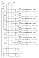
図1は、本発明の第1の実施形態における固体撮像素子2の等価回路図である。本実施形態は、請求項1〜請求項4に対応する。
図に示すように、固体撮像素子2は、ベイヤー配列された赤画素R、緑画素G、青画素Bと、垂直走査回路8と、行毎に各画素と垂直走査回路8とを接続するナンドゲート(NAND GATE)Na1〜Na5及びアンドゲート(AND GATE)An1〜An5と、各画素列毎に配置された垂直信号線VL及び垂直信号線VRと、垂直信号線VLの一端側に接続された定電流源CSLと、垂直信号線VRの一端側に接続された定電流源CSRと、垂直信号線VL、VRの他端側に配置された緑水平信号線20と、赤青水平信号線24と、水平走査回路30とを有している。
Hereinafter, embodiments of the present invention will be described with reference to the drawings. In addition, in each figure, the same code | symbol is attached | subjected to the same element and the overlapping description is abbreviate | omitted.
FIG. 1 is an equivalent circuit diagram of the solid-state imaging device 2 according to the first embodiment of the present invention. This embodiment corresponds to
As shown in the figure, the solid-state imaging device 2 includes a red pixel R, a green pixel G, and a blue pixel B arranged in a Bayer array, a vertical scanning circuit 8, and a NAND gate that connects each pixel and the vertical scanning circuit 8 for each row. (NAND GATE) Na1 to Na5 and AND GATEs An1 to An5, vertical signal lines VL and vertical signal lines VR arranged for each pixel column, and a constant signal connected to one end of the vertical signal line VL. A current source CSL, a constant current source CSR connected to one end side of the vertical signal line VR, a green horizontal signal line 20 disposed on the other end side of the vertical signal lines VL and VR, and a red-blue horizontal signal line 24; , And a
なお、以下の説明では、単に『画素』といった場合、赤画素R、緑画素G、青画素Bの全てを含むものとする。また、図中の符号において先頭がφで始まっているものは駆動電圧を示し、図中のGNDは接地線を示す。図では煩雑となるので画素数を5×4として記載したが、実際にはもっと多くの画素が配列される。
また、図中の一部の要素の符号の最後には、配置行を示すために1、2、3、4、5を付し、配置列との対応関係を示すためにa、b、c、dを付した。ここでの『配置列との対応関係』とは、図の下に数字で示した画素列と、図の上側に示した列選択トランジスタTha〜Thd(機能は後述)等とを比較すれば分かるように、画素の1列目と2列目の間をa列、2列目と3列目の間をb列、3列目と4列目の間をc列、4列目と5列目の間をd列としたものである。なお、奇数行の1列目には、画素は配置されていない。これらa、b、c、dは、後述の回路動作の説明時に各要素を区別し易くするために付したものである。行や列の区別が不要な場合、符号の最後の1、2、a、b等は適宜省略する。
In the following description, the term “pixel” includes all of the red pixel R, the green pixel G, and the blue pixel B. Also, in the reference numerals in the figure, those that start with φ indicate drive voltage, and GND in the figure indicates a ground line. In the figure, the number of pixels is described as 5 × 4 because it is complicated, but actually, more pixels are arranged.
Also, at the end of the reference numerals of some elements in the figure, 1, 2, 3, 4, 5 are added to indicate the arrangement rows, and a, b, c are shown to indicate the correspondence with the arrangement columns. , D. Here, the “correspondence with the arrangement column” can be understood by comparing the pixel columns indicated by numbers at the bottom of the figure with the column selection transistors Tha to Thd (functions will be described later) shown at the top of the figure. Thus, a column between the first and second columns of pixels is b column between the second column and the third column, c column between the third column and the fourth column, fourth column and fifth column The distance between the eyes is d columns. Note that no pixels are arranged in the first column of the odd rows. These a, b, c, and d are given to make it easy to distinguish each element when the circuit operation described later is described. When it is not necessary to distinguish between rows and columns, the last 1, 2, a, b, etc. of the reference numerals are omitted as appropriate.
ここまでの構成において従来と大きく異なるのは、以下の2点である。第1に、各画素列の間には、2本の垂直信号線(VL、VR)が配置されている。なお、図では、1つの画素列に対し垂直走査回路8側(左側)とその反対側に1本ずつ垂直信号線が延在すると見て、垂直走査回路8側のものを垂直信号線VL、反対側のものを垂直信号線VRと定義した。第2に、各画素と垂直走査回路8と間には、ナンドゲートNa及びアンドゲートAnが行毎に配置されている。この第2の特徴については、後述の図2を用いて説明する。 In the configuration so far, the following two points are greatly different from the conventional one. First, two vertical signal lines (VL, VR) are arranged between the pixel columns. In the figure, it is assumed that one vertical signal line extends on the vertical scanning circuit 8 side (left side) and on the opposite side with respect to one pixel column, and the vertical scanning circuit 8 side is connected to the vertical signal line VL, The opposite side was defined as a vertical signal line VR. Second, a NAND gate Na and an AND gate An are arranged for each row between each pixel and the vertical scanning circuit 8. The second feature will be described with reference to FIG.
また、垂直信号線VL及び垂直信号線VRの他端には、本実施形態のもう1つの特徴である緑用選択回路MXG及び赤青用選択回路MXR/Bが、列順次に交互に配置されている。最も端の画素列に対して配置されているものを除き、垂直信号線VLの他端は、入力信号線Iα、Iγの2つに分岐しており、垂直信号線VRの他端は、入力信号線Iβ、Iδの2つに分岐している。入力信号線Iα、Iβ、Iγ、Iδは、どれも、緑用選択回路MXGまたは赤青用選択回路MXR/Bのいずれかに対してのみ接続されている。 Further, at the other end of the vertical signal line VL and the vertical signal line VR, another green selection circuit MXG and red / blue selection circuit MXR / B, which are another feature of the present embodiment, are alternately arranged in the column order. ing. The other end of the vertical signal line VL is branched into two input signal lines Iα and Iγ, except for the one arranged for the endmost pixel column, and the other end of the vertical signal line VR is input. The signal lines Iβ and Iδ are branched into two. The input signal lines Iα, Iβ, Iγ, and Iδ are all connected only to either the green selection circuit MXG or the red / blue selection circuit MXR / B.
そして、a列の緑用選択回路MXGaには、a列に対応する列である1、2列目の緑画素Gの画素信号が入力される。この例では、奇数行の2列目の緑画素G、偶数行の1列目の緑画素Gの画素信号が入力される。また、b列の赤青用選択回路MXR/Bbには、b列に対応する列である2、3列目の赤画素R及び青画素Bの画素信号が入力される。この例では、奇数行の3列目の赤画素Rと、偶数行の2列目の青画素Bの画素信号が入力される。他の列の緑用選択回路MXG、赤青用選択回路MXR/Bdについても同様である。 Then, the pixel signals of the green pixels G in the first and second columns, which are columns corresponding to the a column, are input to the green selection circuit MXGa in the a column. In this example, the pixel signals of the second green pixel G in the odd row and the first green pixel G in the even row are input. In addition, the pixel signals of the red and blue pixels R and B in the second and third columns, which are columns corresponding to the b column, are input to the b / red selection circuit MXR / Bb. In this example, pixel signals of the red pixel R in the third column of the odd row and the blue pixel B in the second column of the even row are input. The same applies to the green selection circuits MXG and red / blue selection circuits MXR / Bd in the other columns.
各緑用選択回路MXGには、相関二重サンプリング処理により各画素の画素信号を受けるCDSコンデンサCcL、CcRが並列接続されている。また、各赤青用選択回路MXR/Bにも、CDSコンデンサCcL、CcRが並列接続されている。このように、1つの画素列当たりに2つのCDSコンデンサCcL、CcRが配置されていることも、本実施形態の特徴の1つである。 Each green selection circuit MXG is connected in parallel with CDS capacitors CcL and CcR that receive a pixel signal of each pixel by correlated double sampling processing. Further, CDS capacitors CcL and CcR are also connected in parallel to each of the red / blue selection circuits MXR / B. As described above, one of the features of this embodiment is that two CDS capacitors CcL and CcR are arranged per pixel column.
また、各緑用選択回路MXG、各赤青用選択回路MXR/Bに対しては、相関二重サンプリング処理を行うための1つのCDSトランジスタTcが配置されている。全てのCDSトランジスタTcは、共通のFPN蓄積パルスφcをゲートに受けて、導通または非導通状態に切り替わる。
さらに、各緑用選択回路MXGに接続されたCDSコンデンサCcL、CcRを緑水平信号線20に接続し、各赤青用選択回路MXR/Bに接続されたCDSコンデンサCcL、CcRを赤青水平信号線24に接続する複数の列選択トランジスタThが配置されている。列選択トランジスタThは、そのゲートに、2列毎に共通の駆動電圧φGHを水平走査回路30から受けて、導通または非導通状態に切り替わる。
Further, one CDS transistor Tc for performing correlated double sampling processing is arranged for each green selection circuit MXG and each red / blue selection circuit MXR / B. All the CDS transistors Tc are switched to a conductive or non-conductive state by receiving a common FPN accumulation pulse φc at their gates.
Further, the CDS capacitors CcL and CcR connected to the green selection circuits MXG are connected to the green horizontal signal line 20, and the CDS capacitors CcL and CcR connected to the red and blue selection circuits MXR / B are connected to the red-blue horizontal signal. A plurality of column selection transistors Th connected to the line 24 are arranged. The column selection transistor Th receives a driving voltage φGH common to every two columns from the
また、緑水平信号線20、赤青水平信号線24における出力端には、出力バッファアンプ32、34と、出力端子Gout、R/Boutと、水平リセットトランジスタTRg、TRrbとがそれぞれ接続されている。水平リセットトランジスタTRg、TRrbは、どちらも、水平リセットパルス電圧φRSTHをゲートに受けて、導通または非導通状態になる。
Further,
図の5行2列目の緑画素Gに符号を示すように、各画素は、フォトダイオードPDと、転送ゲートFWと、リセットゲートRGと、画素アンプである接合型電界効果トランジスタJFET(以下、JFETと略記)とを有している。
転送ゲートFWは、Pチャネル型のMOSトランジスタとして形成されており、ゲート電圧に応じてフォトダイオードPDの蓄積電荷をJFETのゲートに転送する。リセットゲートRGは、Pチャネル型のMOSトランジスタとして形成されている。リセットゲートRGは、オン(導通)状態になることでJFETのゲートを全画素共通の電源(電圧VRD)に接続し、JFETを非動作状態にする。リセットゲートRGがオフ(非導通)のとき、JFETは動作状態となる。JFETのドレインは、全画素共通に基板電位Vsubを受ける。
As shown in the green pixel G in the fifth row and the second column in the figure, each pixel includes a photodiode PD, a transfer gate FW, a reset gate RG, and a junction field effect transistor JFET (hereinafter referred to as a pixel amplifier). Abbreviated as JFET).
The transfer gate FW is formed as a P-channel type MOS transistor, and transfers the accumulated charge of the photodiode PD to the gate of the JFET according to the gate voltage. The reset gate RG is formed as a P-channel type MOS transistor. When the reset gate RG is turned on (conductive), the gate of the JFET is connected to the power supply (voltage VRD) common to all the pixels, and the JFET is inactivated. When the reset gate RG is off (non-conducting), the JFET is in an operating state. The drain of the JFET receives the substrate potential Vsub common to all pixels.
図2は、図1における垂直走査回路8と各画素との接続部分に着目した回路図である。垂直走査回路8は、画素の各行当たりに1本の出力信号線を有し、これら出力信号線は、垂直走査回路8からの行選択信号OPT1〜OPTnをそれぞれ出力する。行選択信号OPTは、画素の各行当たりに1つずつ配置されたナンドゲートNa及びアンドゲートAnの一方の入力端子に入力される。 FIG. 2 is a circuit diagram focusing on the connection between the vertical scanning circuit 8 and each pixel in FIG. The vertical scanning circuit 8 has one output signal line for each row of pixels, and these output signal lines output row selection signals OPT1 to OPTn from the vertical scanning circuit 8, respectively. The row selection signal OPT is input to one input terminal of a NAND gate Na and an AND gate An arranged one for each row of pixels.
図に示すように、奇数行においては、ナンドゲートNaの他方の入力端子は駆動電圧φTG1を受け、アンドゲートAnの他方の入力端子は駆動電圧φRSG1を受ける。また、偶数行においては、ナンドゲートNaの他方の入力端子は駆動電圧φTG2を受け、アンドゲートAnの他方の入力端子は駆動電圧φRSG2を受ける。ある行のナンドゲートNaの出力電圧は、その行の全画素の転送ゲートFWに共通に供給され、ある行のアンドゲートAnの出力電圧は、その行の全画素のリセットゲートRGに共通に供給される。そして、垂直走査回路8により選択される行では、行選択信号OPTは高レベルにされ、選択されない行においては、行選択信号OPTは低レベルにされる。 As shown in the figure, in the odd-numbered row, the other input terminal of the NAND gate Na receives the drive voltage φTG1, and the other input terminal of the AND gate An receives the drive voltage φRSG1. In the even-numbered row, the other input terminal of the NAND gate Na receives the drive voltage φTG2, and the other input terminal of the AND gate An receives the drive voltage φRSG2. The output voltage of the NAND gate Na in a row is supplied in common to the transfer gates FW of all the pixels in the row, and the output voltage of the AND gate An in a row is supplied in common to the reset gates RG of all the pixels in the row. The In a row selected by the vertical scanning circuit 8, the row selection signal OPT is set to a high level, and in a row not selected, the row selection signal OPT is set to a low level.
図3は、緑用選択回路MXG、赤青用選択回路MXR/Bの詳細を示す回路図である。緑用選択回路MXG及び赤青用選択回路MXR/Bは、どちらも同じ回路構成のマルチプレクサであり、定電流源CSML、CSMRと、バイポーラトランジスタBiL、BiRと、nチャネル型のMOSトランジスタであるスイッチQαL、QαR、QβL、QβR、QγL、QγR、QδL、QδRとを有する。なお、図中のVCCは電源線である。 FIG. 3 is a circuit diagram showing details of the green selection circuit MXG and the red / blue selection circuit MXR / B. Both the green selection circuit MXG and the red / blue selection circuit MXR / B are multiplexers having the same circuit configuration, and are constant current sources CSML and CSMR, bipolar transistors BiL and BiR, and switches that are n-channel MOS transistors. QαL, QαR, QβL, QβR, QγL, QγR, QδL, and QδR. In the figure, VCC is a power supply line.
全ての緑用選択回路MXG、及び赤青用選択回路MXR/Bは、共通の8本の信号線を介して、8つの選択用駆動電圧φPαL、φPαR、φPβL、φPβR、φPγL、φPγR、φPδL、φPδRをそれぞれ受ける。
これら8つの選択用駆動電圧φPαL〜φPδRはそれぞれ、高レベルの電圧を受けたとき、対応するスイッチ(QαL〜QδRのいずれか)をオン状態にすることで、対応する入力信号線(Iα〜Iδのいずれか)を対応するCDSコンデンサ(CcL、CcRのいずれか)に接続する。ここでの『対応する』とは、符合に含まれるα、β、γ、δ、L、Rの文字が一致するものである。例えば、選択用駆動電圧φPαRが高レベルのとき、スイッチQαRがオンして、入力信号線IαはCDSトランジスタCcRに接続される。
All the green selection circuits MXG and red / blue selection circuits MXR / B are connected to the eight selection drive voltages φPαL, φPαR, φPβL, φPβR, φPγL, φPγR, φPδL, via eight common signal lines. Each receives φPδR.
Each of these eight selection drive voltages φPαL to φPδR receives a high level voltage, and turns on the corresponding switch (any one of QαL to QδR) to turn on the corresponding input signal line (Iα to Iδ). Is connected to the corresponding CDS capacitor (either CcL or CcR). Here, “corresponding” means that the characters α, β, γ, δ, L, and R included in the code match. For example, when the selection drive voltage φPαR is at a high level, the switch QαR is turned on, and the input signal line Iα is connected to the CDS transistor CcR.
以上の回路構成において、請求項との対応関係は、例えば以下の通りである。
請求項記載の垂直方向は、画素の列方向、即ち、垂直信号線VL、VRの延在方向に対応し、水平方向は、垂直方向に直交する方向(画素の行方向)に対応する。請求項記載の第1、第2、第3色成分画素はそれぞれ、緑画素G、青画素R、赤画素Rに対応する。請求項記載の第1容量対は、緑用選択回路MXGに接続されたCDSコンデンサCcL、CcRに対応し、第2容量対は、赤青用選択回路MXR/Bに接続されたCDSコンデンサCcL、CcRに対応する。
In the above circuit configuration, the correspondence with the claims is, for example, as follows.
The vertical direction described in the claims corresponds to the column direction of the pixels, that is, the extending direction of the vertical signal lines VL and VR, and the horizontal direction corresponds to the direction orthogonal to the vertical direction (pixel row direction). The first, second, and third color component pixels recited in the claims correspond to the green pixel G, the blue pixel R, and the red pixel R, respectively. The first capacitance pair corresponds to the CDS capacitors CcL and CcR connected to the green selection circuit MXG, and the second capacitance pair is the CDS capacitor CcL connected to the red-blue selection circuit MXR / B, Corresponds to CcR.
請求項記載の第1垂直信号線は垂直信号線VRに対応し、第2垂直信号線は垂直信号線VLに対応する。請求項記載の第1水平信号線、第2水平信号線は、それぞれ、緑水平信号線20、赤青水平信号線24に対応する。請求項記載のスイッチング回路は、緑用選択回路MXG、赤青用選択回路MXR/B、列選択トランジスタTh、CDSトランジスタTc、水平リセットトランジスタTRg、TRrb、水平走査回路30に対応する。
The first vertical signal line corresponds to the vertical signal line VR, and the second vertical signal line corresponds to the vertical signal line VL. The first horizontal signal line and the second horizontal signal line recited in the claims correspond to the green horizontal signal line 20 and the red-blue horizontal signal line 24, respectively. The switching circuit described in claims corresponds to the green selection circuit MXG, the red / blue selection circuit MXR / B, the column selection transistor Th, the CDS transistor Tc, the horizontal reset transistors TRg and TRrb, and the
図4は、上述の固体撮像素子2において通常読み出しを行う場合、即ち、全画素の画素信号を読み出す場合の各部の電圧波形を示すタイミング図である。以下、図1、図3及び図4を参照しながら固体撮像素子2の回路動作を説明する。
まず、垂直走査回路8における不図示の垂直シフトレジスタを駆動するために、高レベルのスタートパルスSTVを垂直走査回路8に入力する。これにほぼ同期して、低レベルのクロック信号CLKV1と、高レベルのクロック信号CLKV2とを垂直走査回路8に入力する。これにより、垂直走査回路8が出力する行選択信号OPT1は高レベルに切り替わり、他の行選択信号OPT2〜OPTnは低レベルにされ、固体撮像素子2の1行目が選択される。
FIG. 4 is a timing diagram showing voltage waveforms at various portions when normal reading is performed in the solid-state imaging device 2 described above, that is, when pixel signals of all pixels are read. Hereinafter, the circuit operation of the solid-state imaging device 2 will be described with reference to FIGS. 1, 3, and 4.
First, a high level start pulse STV is input to the vertical scanning circuit 8 in order to drive a vertical shift register (not shown) in the vertical scanning circuit 8. Almost in synchronization with this, a low level
なお、クロック信号CLKV1、CLKV2の入力直後において、駆動電圧φRSG1、φRSG2、φTG1、φTG2は全て低レベルである。従って、全行において、ナンドゲートNaの出力電圧は高レベルであるので転送ゲートFWはオフ状態であり、また、アンドゲートの出力電圧は低レベルであるので、リセットゲートRGはオン状態であり、JFETのゲート電圧はリセットされている。他の行の選択直後においても同様である。 Note that immediately after the clock signals CLKV1 and CLKV2 are input, the drive voltages φRSG1, φRSG2, φTG1, and φTG2 are all at a low level. Accordingly, in all the rows, the output voltage of the NAND gate Na is high, so that the transfer gate FW is off, and the output voltage of the AND gate is low, so that the reset gate RG is on, and the JFET The gate voltage is reset. The same applies immediately after selection of another row.
次に、8つの選択用駆動電圧の内、φPδL、φPδRのみを高レベルにする。これにより、緑用選択回路MXGに接続されたCDSコンデンサCcL、CcRは、入力信号線Iδ、垂直信号線VRを介して1行目の緑画素GのJFETのソースに接続される。また、赤青用選択回路MXR/Bに接続されたCDSコンデンサCcL、CcRは、入力信号線Iδ、垂直信号線VRを介して1行目の赤画素RのJFETのソースに接続される。 Next, among the eight selection drive voltages, only φPδL and φPδR are set to a high level. As a result, the CDS capacitors CcL and CcR connected to the green selection circuit MXG are connected to the JFET source of the green pixel G in the first row via the input signal line Iδ and the vertical signal line VR. The CDS capacitors CcL and CcR connected to the red / blue selection circuit MXR / B are connected to the source of the JFET of the red pixel R in the first row via the input signal line Iδ and the vertical signal line VR.
次に、駆動電圧φRSG1を高レベルに切り替える。これにより、垂直走査回路8により選択されている1行目のアンドゲートAn1の出力電圧は高レベルに切り替わり、1行目のリセットゲートRGはオフする。駆動電圧φRSG1が高レベルに切り替わる過程において、JFETのゲートは、電気的にフローティング状態になると共に、容量結合によって電圧が上昇する。この容量結合は、JFETのゲートが隣接する領域(ソース、ドレイン、転送ゲートFW等)との間に形成する容量により生じる。 Next, the drive voltage φRSG1 is switched to a high level. As a result, the output voltage of the AND gate An1 in the first row selected by the vertical scanning circuit 8 is switched to a high level, and the reset gate RG in the first row is turned off. In the process in which the drive voltage φRSG1 is switched to a high level, the gate of the JFET is in an electrically floating state and the voltage rises due to capacitive coupling. This capacitive coupling is caused by the capacitance formed between the adjacent regions (source, drain, transfer gate FW, etc.) of the JFET gate.
次に、FPN蓄積パルスφcを高レベルに切り替え、全てのCDSトランジスタTcをオンする。このときはまだ、JFETのゲートにはフォトダイオードPDの信号電荷が転送されていないので、JFETのソース電圧は、固定パターンノイズ成分に相当する電圧である。従って、CDSコンデンサCcL、CcRにおける画素側の電極の充電電圧は、どちらも、(固定パターンノイズ成分−Vref)となる。この後、FPN蓄積パルスφcを低レベルに切り替える。 Next, the FPN accumulation pulse φc is switched to a high level, and all the CDS transistors Tc are turned on. At this time, since the signal charge of the photodiode PD has not yet been transferred to the gate of the JFET, the source voltage of the JFET is a voltage corresponding to a fixed pattern noise component. Therefore, the charging voltage of the pixel-side electrode in the CDS capacitors CcL and CcR is both (fixed pattern noise component −Vref). Thereafter, the FPN accumulation pulse φc is switched to a low level.
次に、駆動電圧φTG1を高レベルに切り替える。これにより、1行目では、ナンドゲートNa1の出力電圧が低レベルに切り替わり、各転送ゲートFWがオンし、フォトダイオードPDの信号電荷はJFETのゲートに転送される。JFETは、ゲート内の蓄積電荷量に応じた信号電圧(画素信号)をソースから出力する。これにより、CDSコンデンサCcL、CcRにおけるCDSトランジスタTc側の電極の電圧は、どちらも、次式で示される同じ電圧に充電される。
[信号電圧−(固定パターンノイズ成分−Vref)]・・・(1)
即ち、信号電圧には固定パターンノイズ成分が含まれているが、先にFPN蓄積パルスφcにより充電した電圧により、固定パターンノイズ成分は相殺される(相関二重サンプリング処理)。この後、駆動電圧φTG1を低レベルに切り替える。
Next, the drive voltage φTG1 is switched to a high level. Thereby, in the first row, the output voltage of the NAND gate Na1 is switched to a low level, each transfer gate FW is turned on, and the signal charge of the photodiode PD is transferred to the gate of the JFET. The JFET outputs a signal voltage (pixel signal) corresponding to the amount of charge accumulated in the gate from the source. As a result, the voltages of the electrodes on the CDS transistor Tc side in the CDS capacitors CcL and CcR are both charged to the same voltage expressed by the following equation.
[Signal voltage-(fixed pattern noise component-Vref)] (1)
That is, the fixed voltage noise component is included in the signal voltage, but the fixed pattern noise component is canceled by the voltage previously charged by the FPN accumulation pulse φc (correlated double sampling processing). Thereafter, the drive voltage φTG1 is switched to a low level.
次に、駆動電圧φRSG1が高レベルである残りの期間内において、1行目の画素信号の水平方向の読み出しが行われる。水平方向の読み出しは、緑水平信号線20及び赤青水平信号線24の電圧をリセットする動作と、水平走査回路30内の不図示の水平シフトレジスタを1つずつ順送りにオンしていく動作とを繰り返すことで行われる。具体的にはまず、水平リセットパルス電圧φRSTHを高レベルに切り替える。これにより、水平リセットトランジスタTRg、TRrbはオンして、緑水平信号線20及び赤青水平信号線24の電圧はVrefにリセットされる。この後、水平リセットパルス電圧φRSTHを低レベルに切り替える。
Next, the pixel signals in the first row are read in the horizontal direction within the remaining period in which the drive voltage φRSG1 is at a high level. The horizontal reading includes an operation of resetting the voltages of the green horizontal signal line 20 and the red / blue horizontal signal line 24, and an operation of turning on a horizontal shift register (not shown) in the
次に、水平走査回路30における最も出力バッファアンプ32側の水平シフトレジスタをオンさせ、a、b列に対応する駆動電圧φGHabを高レベルに切り替える。これにより、列選択トランジスタTha、Thbをオン状態に切り替える。これにより、a列の緑用選択回路MXGaに接続されたCDSコンデンサCcL、CcRの充電電圧(画素信号に相当)は、緑水平信号線20、出力バッファアンプ32を介して出力される。また、b列の赤青用選択回路MXR/Bbに接続されたCCDSコンデンサCcL、CcRに充電した画素信号は、赤青水平信号線24、出力バッファアンプ34を介して出力される。
Next, the horizontal shift register closest to the
ここで、緑水平信号線20に出力される信号電圧について補足説明をする。JFETのソースの出力電圧値をJS、CDSコンデンサCcL、CcRの容量値(ファラド)をそれぞれCF1、CF2とすれば、並列接続された一対のCDSコンデンサCcL、CcRの合計の蓄積電荷量(クーロン)は、JS×(CF1+CF2)である。ここで、緑水平信号線20には寄生容量が存在するので、この容量値をCFHとすれば、CFHにも蓄積電荷が分配される分だけ信号電圧が低くなるのと等価になる。即ち、緑水平信号線20の出力電圧Vsgは、次式のようになる。
Vsg=JS×(CF1+CF2)/(CF1+CF2+CFH)・・・(2)
赤青水平信号線24も同様に寄生容量を有し、赤青水平信号線24の出力電圧も(2)式と同様になる。なお、本実施形態では一例として、CF1=CF2である。
Here, a supplementary description will be given of the signal voltage output to the green horizontal signal line 20. If the output voltage value of the source of the JFET is JS and the capacitance values (farads) of the CDS capacitors CcL and CcR are CF1 and CF2, respectively, the total accumulated charge amount (coulomb) of the pair of CDS capacitors CcL and CcR connected in parallel Is JS × (CF1 + CF2). Here, since there is a parasitic capacitance in the green horizontal signal line 20, if the capacitance value is CFH, it is equivalent to the signal voltage being lowered by the amount that the accumulated charge is distributed to CFH. That is, the output voltage Vsg of the green horizontal signal line 20 is expressed by the following equation.
Vsg = JS × (CF1 + CF2) / (CF1 + CF2 + CFH) (2)
Similarly, the red-blue horizontal signal line 24 has a parasitic capacitance, and the output voltage of the red-blue horizontal signal line 24 is the same as that in the expression (2). In the present embodiment, as an example, CF1 = CF2.
上記のようにして1行目における2列目、3列目の画素信号を緑水平信号線20、赤青水平信号線24にそれぞれ読み出した後、水平リセットパルス電圧φRSTHを高レベルに切り替える(前述したように奇数行1列目には画素はなく、読み出されない)。これにより、緑水平信号線20及び赤青水平信号線24の電圧をリセットした後、水平リセットパルス電圧φRSTHを低レベルに切り替える。 After the pixel signals in the second and third columns in the first row are read to the green horizontal signal line 20 and the red / blue horizontal signal line 24 as described above, the horizontal reset pulse voltage φRSTH is switched to a high level (described above). As described above, there is no pixel in the odd-numbered row and the first column and is not read out). Thereby, after resetting the voltages of the green horizontal signal line 20 and the red-blue horizontal signal line 24, the horizontal reset pulse voltage φRSTH is switched to a low level.
そして、水平シフトレジスタが1つシフトし、c、d列に対応する駆動電圧φGHcdが高レベルに切り替わり、列選択トランジスタThc、Thdがオンする。これにより、c列の緑用選択回路MXGcに接続されたCDSコンデンサCcL、CcRに充電した画素信号は、緑水平信号線20に出力され、d列の赤青用選択回路MXR/Bdに接続されたCDSコンデンサCcL、CcRに充電した画素信号は、青水平信号線に出力される。即ち、1行目における4列目、5列目の画素信号が読み出される。 Then, the horizontal shift register is shifted by one, the drive voltage φGHcd corresponding to the columns c and d is switched to a high level, and the column selection transistors Thc and Thd are turned on. Thereby, the pixel signals charged in the CDS capacitors CcL and CcR connected to the green selection circuit MXGc in the c column are output to the green horizontal signal line 20 and connected to the red / blue selection circuit MXR / Bd in the d column. The pixel signals charged in the CDS capacitors CcL and CcR are output to the blue horizontal signal line. That is, the pixel signals in the fourth column and the fifth column in the first row are read out.
このような動作を繰り返すことにより、1行目の画素信号の読み出しを2列毎に行った後、駆動電圧φRSG1を低レベルに切り替える。これにより、1行目においては、アンドゲートAn1の出力電圧が低レベルに切り替わり、リセットゲートRGはオフ状態に切り替わり、JFETのゲート電圧はリセットされる。ここまでが図4における『1行目水平読み出し』の期間である。 By repeating such an operation, the pixel signal in the first row is read every two columns, and then the drive voltage φRSG1 is switched to a low level. As a result, in the first row, the output voltage of the AND gate An1 is switched to a low level, the reset gate RG is switched to the OFF state, and the gate voltage of the JFET is reset. This is the period of “first row horizontal reading” in FIG.
次に、クロック信号CLKV1、CLKV2を垂直走査回路8に入力して垂直シフトレジスタを1つシフトさせ、2行目を選択する。次に、8つの選択用駆動電圧の内、φPβL、φPβRのみを高レベルにする。これにより、緑用選択回路MXGに接続されたCDSコンデンサCcL、CcRは、入力信号線Iβ、垂直信号線VRを介して2行目の緑画素Gに接続される。また、赤青用選択回路MXR/Bに接続されたCDSコンデンサCcL、CcRは、入力信号線Iβ、垂直信号線VRを介して2行目の青画素Bに接続される。 Next, the clock signals CLKV1 and CLKV2 are input to the vertical scanning circuit 8 to shift the vertical shift register by one and select the second row. Next, of the eight selection drive voltages, only φPβL and φPβR are set to a high level. As a result, the CDS capacitors CcL and CcR connected to the green selection circuit MXG are connected to the green pixels G in the second row via the input signal line Iβ and the vertical signal line VR. The CDS capacitors CcL and CcR connected to the red / blue selection circuit MXR / B are connected to the blue pixels B in the second row through the input signal line Iβ and the vertical signal line VR.
次に、駆動電圧φRSG2を高レベルに切り替える。この後、駆動電圧φTG1の代わりにφTG2を高レベルにすることを除き、1行目の場合と同様に2行目の画素信号を読み出す。即ち、緑用選択回路MXGに接続されたCDSコンデンサCcL、CcRは、どちらも2行目の緑画素Gの画素信号により充電され、この画素信号は、緑水平信号線20から読み出される。同時に、赤青用選択回路MXR/Bに接続されたCDSコンデンサCcL、CcRは、どちらも2行目の青画素Bの画素信号により充電され、この画素信号は、赤青平信号線24から読み出される。これにより、2行目の読み出しを終了する。 Next, the drive voltage φRSG2 is switched to a high level. Thereafter, pixel signals in the second row are read out in the same manner as in the first row, except that φTG2 is set to a high level instead of the drive voltage φTG1. That is, the CDS capacitors CcL and CcR connected to the green selection circuit MXG are both charged by the pixel signal of the green pixel G in the second row, and this pixel signal is read from the green horizontal signal line 20. At the same time, the CDS capacitors CcL and CcR connected to the red / blue selection circuit MXR / B are both charged by the pixel signal of the blue pixel B in the second row, and this pixel signal is read from the red / blue flat signal line 24. . Thereby, the reading of the second row is completed.
次に、クロック信号CLKV1、CLKV2を垂直走査回路8に入力し、3行目を選択する。次に、8つの制御用駆動電圧の内、φPγL、φPγRのみを高レベルにする。これにより、緑用選択回路MXGに接続されたCDSコンデンサCcL、CcRは、入力信号線Iγ、垂直信号線VLを介して3行目の緑画素Gに接続される。また、赤青用選択回路MXR/Bに接続されたCDSコンデンサCcL、CcRは、入力信号線Iγ、垂直信号線VLを介して3行目の赤画素Rに接続される。この後、駆動電圧φRSG1を高レベルに切り替え、1行目の場合と同様に3行目の画素信号を読み出す。 Next, the clock signals CLKV1 and CLKV2 are input to the vertical scanning circuit 8 to select the third row. Next, of the eight control drive voltages, only φPγL and φPγR are set to a high level. As a result, the CDS capacitors CcL and CcR connected to the green selection circuit MXG are connected to the green pixels G in the third row via the input signal line Iγ and the vertical signal line VL. The CDS capacitors CcL and CcR connected to the red / blue selection circuit MXR / B are connected to the red pixel R in the third row via the input signal line Iγ and the vertical signal line VL. Thereafter, the drive voltage φRSG1 is switched to a high level, and the pixel signals in the third row are read out as in the case of the first row.
次に、クロック信号CLKV1、CLKV2を垂直走査回路8に入力し、4行目を選択する。次に、8つの制御用駆動電圧の内、φPαL、φPαRのみを高レベルにする。これにより、緑用選択回路MXGに接続されたCDSコンデンサCcL、CcRは、入力信号線Iα、垂直信号線VLを介して4行目の緑画素Gに接続される。また、赤青用選択回路MXR/Bに接続されたCDSコンデンサCcL、CcRは、入力信号線Iα、垂直信号線VLを介して4行目の青画素Bに接続される。次に、駆動電圧φRSG2を高レベルに切り替え、2行目の場合と同様に4行目の画素信号を読み出す。 Next, the clock signals CLKV1 and CLKV2 are input to the vertical scanning circuit 8, and the fourth row is selected. Next, of the eight control drive voltages, only φPαL and φPαR are set to a high level. As a result, the CDS capacitors CcL and CcR connected to the green selection circuit MXG are connected to the fourth row of green pixels G via the input signal line Iα and the vertical signal line VL. The CDS capacitors CcL and CcR connected to the red / blue selection circuit MXR / B are connected to the blue pixels B in the fourth row via the input signal line Iα and the vertical signal line VL. Next, the drive voltage φRSG2 is switched to a high level, and the pixel signals in the fourth row are read out as in the case of the second row.
以上の動作を繰り返して、全行の画素信号を読み出す。読み出し走査は、4行単位で同じになり、その4行における主な違いは、以下の2点である。第1に、奇数行では駆動電圧φRSG1、φTG1を用い、偶数行では駆動電圧φRSG2、φTG2を用いる。第2に、8つの制御用駆動電圧のどれを高レベルにするかが異なる。即ち、(4n−3)行目が選択されていればφPδL、φPδRを高レベルにし、(4n−2)行目が選択されていればφPβL、φPβRを高レベルにし、(4n−1)行目が選択されていればφPγL、φPγRを高レベルにし、4n行目が選択されていればφPαL、φPαRを高レベルにする。以上が通常読み出しの動作説明である。 By repeating the above operation, pixel signals of all rows are read out. The readout scanning is the same in units of four rows, and the main differences in the four rows are the following two points. First, the driving voltages φRSG1 and φTG1 are used in the odd rows, and the driving voltages φRSG2 and φTG2 are used in the even rows. Second, which of the eight control drive voltages is set to a high level is different. That is, if the (4n-3) th row is selected, φPδL and φPδR are set to a high level, and if the (4n-2) th row is selected, φPβL and φPβR are set to a high level. If the eye is selected, φPγL and φPγR are set to a high level, and if the 4nth row is selected, φPαL and φPαR are set to a high level. The above is the description of the normal reading operation.
図5は、上述の固体撮像素子2において間引き読み出しを行う場合の各部の電圧波形を示すタイミング図である。以下、図1、図3及び図5を参照しながら、間引き読み出しの回路動作を説明する。
まず、通常読み出しの場合と同様に高レベルのスタートパルスSTV、クロック信号CLKV1、CLKV2を垂直走査回路8に入力し、1行目のみを選択する。この後、クロック信号CLKV1、CLKV2を入力し、2行目のみを選択する。この後、スタートパルスSTV、クロック信号CLKV1、CLKV2をほぼ同時に垂直走査回路8に入力する。これにより、1行目と3行目が同時に選択される。なお、通常読み出しの場合と同様に、クロック信号CLKV1、CLKV2の入力直後では、全行において、転送ゲートFWはオフしており、JFETのゲート電圧はリセットされている。
FIG. 5 is a timing diagram showing voltage waveforms at various parts when thinning readout is performed in the solid-state imaging device 2 described above. Hereinafter, the circuit operation of thinning readout will be described with reference to FIG. 1, FIG. 3, and FIG.
First, the high level start pulse STV and the clock signals CLKV1 and CLKV2 are input to the vertical scanning circuit 8 as in the case of normal reading, and only the first row is selected. Thereafter, clock signals CLKV1 and CLKV2 are input, and only the second row is selected. Thereafter, the start pulse STV and the clock signals CLKV1 and CLKV2 are input to the vertical scanning circuit 8 almost simultaneously. As a result, the first and third rows are selected simultaneously. As in the case of normal reading, immediately after the clock signals CLKV1 and CLKV2 are input, the transfer gates FW are turned off and the gate voltages of the JFETs are reset in all rows.
次に、8つの選択用駆動電圧の内、φPδL、φPγRのみを高レベルにする。これにより、緑用選択回路MXGに接続されたCDSコンデンサの内、CcLは、入力信号線Iδ、垂直信号線VRを介して1行目の緑画素Gに接続され、CcRは、入力信号線Iγ、垂直信号線VLを介して3行目の緑画素Gに接続される。また、赤青用選択回路MXR/Bに接続されたCDSコンデンサの内、CcLは、入力信号線Iδ、垂直信号線VRを介して1行目の赤画素Rに接続され、CcRは、入力信号線Iγ、垂直信号線VLを介して3行目の赤画素Rに接続される。 Next, of the eight selection drive voltages, only φPδL and φPγR are set to a high level. Accordingly, among the CDS capacitors connected to the green selection circuit MXG, CcL is connected to the green pixel G in the first row via the input signal line Iδ and the vertical signal line VR, and CcR is connected to the input signal line Iγ. Are connected to the green pixel G in the third row via the vertical signal line VL. Among the CDS capacitors connected to the red / blue selection circuit MXR / B, CcL is connected to the red pixel R in the first row via the input signal line Iδ and the vertical signal line VR, and CcR is the input signal. The line is connected to the red pixel R in the third row via the line Iγ and the vertical signal line VL.
次に、駆動電圧φRSG1を高レベルに切り替えて、選択されている1、3行目のJFETを動作状態にする。次に、FPN蓄積パルスφcを高レベルに切り替えて、CDSトランジスタTcをオンする。これにより、CDSコンデンサCcL、CcRには、それぞれ、上記のように接続された1つの画素の固定パターンノイズ成分に相当する電圧が充電される。この後、FPN蓄積パルスφcを低レベルに切り替える。 Next, the drive voltage φRSG1 is switched to a high level, and the selected JFETs in the first and third rows are set in an operating state. Next, the FPN accumulation pulse φc is switched to a high level to turn on the CDS transistor Tc. Thereby, the CDS capacitors CcL and CcR are each charged with a voltage corresponding to the fixed pattern noise component of one pixel connected as described above. Thereafter, the FPN accumulation pulse φc is switched to a low level.
次に、駆動電圧φTG1を高レベルに切り替える。これにより、1、3行目の画素の転送ゲートFWがオンし、フォトダイオードPDの信号電荷はJFETのゲートに転送され、JFETは、信号電圧(画素信号)をソースから出力する。これにより、CDSコンデンサCcL、CcRには、それぞれ、1つの画素の画素信号が充電される。このとき、先に充電した固定パターンノイズ成分が相殺される。この後、駆動電圧φTG1を低レベルに切り替える。 Next, the drive voltage φTG1 is switched to a high level. As a result, the transfer gates FW of the pixels in the first and third rows are turned on, the signal charge of the photodiode PD is transferred to the gate of the JFET, and the JFET outputs a signal voltage (pixel signal) from the source. Thereby, the CDS capacitors CcL and CcR are each charged with a pixel signal of one pixel. At this time, the previously charged fixed pattern noise component is canceled out. Thereafter, the drive voltage φTG1 is switched to a low level.
次に、駆動電圧φRSG1が高レベルである残りの期間内において、通常読み出しの場合と同様の走査により、1、3行目における全列の画素信号を水平方向に読み出す。なお、CDSコンデンサCcL、CcRにはそれぞれ、1行目と3行目の画素信号を充電したので、緑水平信号線20及び赤青水平信号線24に出力される信号電圧は、通常読み出しの場合とは異なり、1行目と3行目の画素信号が合算平均されたものとなる。 Next, in the remaining period in which the drive voltage φRSG1 is at a high level, the pixel signals of all the columns in the first and third rows are read in the horizontal direction by the same scanning as in the normal reading. Since the CDS capacitors CcL and CcR are charged with the pixel signals in the first row and the third row, the signal voltages output to the green horizontal signal line 20 and the red-blue horizontal signal line 24 are in the case of normal reading. Unlike the above, the pixel signals in the first and third rows are summed and averaged.
具体的には、1行目のJFETのソースの出力電圧値をJS1、3行目のJFETのソースの出力電圧値をJS3とすれば、並列接続された一対のCDSコンデンサCcL、CcRの合計の蓄積電荷量は、(JS1×CF1+JS3×CF2)である。ここで、緑水平信号線20の寄生容量CFHを考慮すれば、緑水平信号線20の出力電圧Vsgは、次式のようになる。 Specifically, if the output voltage value of the source of the JFET in the first row is JS1, and the output voltage value of the source of the JFET in the third row is JS3, the total of the pair of CDS capacitors CcL and CcR connected in parallel The accumulated charge amount is (JS1 × CF1 + JS3 × CF2). Here, when the parasitic capacitance CFH of the green horizontal signal line 20 is taken into consideration, the output voltage Vsg of the green horizontal signal line 20 is expressed by the following equation.
Vsg=(JS1×CF1+JS3×CF2)/(CF1+CF2+CFH)
・・・(3)
即ち、本実施形態ではCF1とCF2は等しいので、寄生容量CFHの影響を除けば、2つのCDSコンデンサCcL、CcRの充電電圧が合算平均されて出力されることと等価になる。赤青水平信号線24の出力電圧も(3)式と同様になる。1、3行目の画素信号の水平方向の読み出しが終了すると、駆動電圧φRSG1を低レベルに切り替える。ここまでが図5における『1、3行目水平読み出し』の期間である。
Vsg = (JS1 × CF1 + JS3 × CF2) / (CF1 + CF2 + CFH)
... (3)
In other words, since CF1 and CF2 are equal in this embodiment, if the influence of the parasitic capacitance CFH is removed, it is equivalent to the sum of the charging voltages of the two CDS capacitors CcL and CcR being output. The output voltage of the red / blue horizontal signal line 24 is the same as that in the expression (3). When the horizontal readout of the pixel signals in the first and third rows is completed, the drive voltage φRSG1 is switched to a low level. This is the “1st, 3rd row horizontal readout” period in FIG.
次に、クロック信号CLKV1、CLKV2を1パルスずつ垂直走査回路8に入力し、垂直シフトレジスタを1つシフトさせ、2行目と4行目を同時に選択する。
次に、8つの選択用駆動電圧の内、φPαL、φPαRのみを高レベルにする。これにより、緑用選択回路MXGに接続されたCDSコンデンサCcL、CcRは、入力信号線Iα、垂直信号線VLを介して4行目の緑画素Gに接続される。また、赤青用選択回路MXR/Bに接続されたCDSコンデンサCcL、CcRは、入力信号線Iα、垂直信号線VLを介して4行目の青画素Bに接続される。即ち、2行目と4行目が選択されているが、2行目は読み出されず、4行目の画素信号のみが単独で読み出される。この後、駆動電圧φRSG2を高レベルに切り替え、通常読み出しにおける4行目の場合と同様に4行目の画素信号を読み出した後、駆動電圧φRSG2を低レベルに切り替える。
Next, the clock signals CLKV1 and CLKV2 are input to the vertical scanning circuit 8 one pulse at a time, the vertical shift register is shifted by one, and the second and fourth rows are selected simultaneously.
Next, of the eight selection drive voltages, only φPαL and φPαR are set to a high level. As a result, the CDS capacitors CcL and CcR connected to the green selection circuit MXG are connected to the fourth row of green pixels G via the input signal line Iα and the vertical signal line VL. The CDS capacitors CcL and CcR connected to the red / blue selection circuit MXR / B are connected to the blue pixels B in the fourth row via the input signal line Iα and the vertical signal line VL. That is, the second and fourth rows are selected, but the second row is not read, and only the pixel signals of the fourth row are read alone. Thereafter, the drive voltage φRSG2 is switched to a high level, and the pixel signal in the fourth row is read out as in the case of the fourth row in normal readout, and then the drive voltage φRSG2 is switched to a low level.
次に、クロック信号CLKV1、CLKV2を3パルスずつ垂直走査回路8に入力し、垂直シフトレジスタを3つシフトさせ、5行目と7行目を同時に選択する。この後、8つの選択用駆動電圧の内、φPδL、φPγRのみを高レベルにし、1、3行目の場合と同様に、5、7行目の画素信号を混合読み出しする。
次に、クロック信号CLKV1、CLKV2を1パルスずつ垂直走査回路8に入力し、垂直シフトレジスタを1つシフトさせ、6行目と8行目を同時に選択する。この後、8つの選択用駆動電圧の内、φPαL、φPαRのみを高レベルにし、4行目の場合と同様に、8行目の画素信号を単独で読み出す。
Next, the clock signals CLKV1 and CLKV2 are input to the vertical scanning circuit 8 by three pulses at a time, and the vertical shift register is shifted by three to simultaneously select the fifth and seventh rows. Thereafter, among the eight selection drive voltages, only φPδL and φPγR are set to the high level, and the pixel signals in the fifth and seventh rows are mixed and read out as in the first and third rows.
Next, the clock signals CLKV1 and CLKV2 are input to the vertical scanning circuit 8 one pulse at a time, the vertical shift register is shifted by one, and the sixth and eighth rows are selected simultaneously. Thereafter, among the eight selection drive voltages, only φPαL and φPαR are set to the high level, and the pixel signals in the eighth row are read out independently, as in the case of the fourth row.
以上の動作を繰り返すことで、全行の画素信号を読み出す。読み出し走査は4行単位で同じになる。即ち、選択用駆動電圧の内、φPδL、φPγRを高レベルにし、(4n−3)行目と(4n−1)行目の画素信号を混合読み出しした後、選択用駆動電圧の内、φPαL、φPαRを高レベルにし、4n行目の画素信号を単独で読み出す動作を繰り返す。以上が間引き読み出しの動作説明である。 By repeating the above operation, the pixel signals of all rows are read out. The readout scanning is the same in units of 4 rows. That is, φPδL and φPγR among the selection drive voltages are set to a high level, and the pixel signals of the (4n-3) and (4n-1) rows are mixed and read, and then, among the selection drive voltages, φPαL, The operation of setting φPαR to a high level and reading the pixel signal of the 4nth row independently is repeated. The above is the description of the thinning readout operation.
このように第1の実施形態における間引き読み出しでは、(4n−3)行目と(4n−1)行目を同時に混合読み出しする動作と、4n行目を単独で読み出す動作とを繰り返す。従って、読み出し時間は、全行を1行ずつ読み出す通常読み出しの場合の半分になる。
また、各画素から出力される画素信号は、JFETのソース電圧であり、それをCDSコンデンサCcL、CcRに充電後、電圧として緑水平信号線20、赤青水平信合線24に出力する。従って、電流で読み出す場合よりも、ノイズが小さくなる。
As described above, in the thinning readout in the first embodiment, the operation of simultaneously reading the (4n-3) th and (4n-1) th rows and the operation of reading the 4nth row independently are repeated. Accordingly, the read time is half that of the normal read in which all rows are read one by one.
The pixel signal output from each pixel is the source voltage of the JFET, which is output to the green horizontal signal line 20 and the red / blue horizontal signal line 24 after charging the CDS capacitors CcL and CcR. Therefore, noise is smaller than when reading with current.
(4n−3)行目及び(4n−1)行目の画素信号を合算平均した信号が緑水平信号線20、赤青水平信号線24から出力されるので、両者の内の一方を読み出して他方を読み出さない場合と比較して、2倍の入射光量が画像信号の生成に寄与する。従って、光利用率が高くなる。また、1行跨いで位置する2つの緑画素G(または赤画素R)の画素信号を平均するので、ノイズの大きさは、一方のみを読み出す場合の約1/√2になる。即ち、SN比を約3dB向上できる。 Since a signal obtained by averaging the pixel signals of the (4n-3) th row and the (4n-1) th row is output from the green horizontal signal line 20 and the red / blue horizontal signal line 24, one of them is read out. Compared with the case where the other is not read, twice the amount of incident light contributes to the generation of the image signal. Accordingly, the light utilization rate is increased. Further, since the pixel signals of two green pixels G (or red pixels R) located across one row are averaged, the magnitude of the noise is about 1 / √2 when only one is read out. That is, the SN ratio can be improved by about 3 dB.
ここで、混合読み出しされる(4n−3)行目と(4n−1)行目は、緑画素Gと赤画素Rとが配置された行(以下、GR行という)であり、単独で読み出される4n行目は、緑画素Gと青画素Bとが配置された行(以下、GB行という)である。一般に、青色成分よりも赤色成分の方がモアレが視覚的に目立ちやすいので、GR行に対して混合読み出しする本実施形態では、間引き読み出しの際のモアレやノイズを効果的に低減できる。 Here, the (4n-3) th and (4n-1) th rows that are mixedly read are rows in which green pixels G and red pixels R are arranged (hereinafter referred to as GR rows), and are read out independently. The 4nth row is a row in which the green pixel G and the blue pixel B are arranged (hereinafter referred to as GB row). In general, moire is more visually noticeable in the red component than in the blue component. Therefore, in the present embodiment in which mixed readout is performed with respect to the GR row, moire and noise during thinning readout can be effectively reduced.
(4n−3)行目と(4n−1)行目の画素信号を混合読み出しする場合、サンプリングの重心は、両者の中間である(4n−2)行目になる。そして、4n行目は単独で読み出されるため、サンプリングの重心は、(4n−2)行目、4n行目の繰り返しになるので、間引き読み出し時におけるサンプリング間隔を全行に亘って等しくできる。従って、本実施形態の固体撮像素子2をデジタルカメラに搭載すれば、連写速度を2倍にでき、良好な画像信号が得られる。 When the pixel signals in the (4n-3) th and (4n-1) th rows are mixed and read, the center of gravity of sampling is the (4n-2) th row which is the middle of both. Since the 4n-th row is read out independently, the center of sampling is repeated in the (4n-2) -th row and the 4n-th row, so that the sampling interval at the thinning-out readout can be made equal over all rows. Therefore, if the solid-state imaging device 2 of this embodiment is mounted on a digital camera, the continuous shooting speed can be doubled and a good image signal can be obtained.
なお、第1の実施形態の間引き読み出しでは、GR行に対しては混合読み出しを行い、GB行は単独で読み出す例を述べた。本発明は、かかる実施形態に限定されるものではない。GR行である(4n−3)行目を単独で読み出す動作と、GB行である(4n−2)行目、4n行目を混合読み出しする動作とを順次繰り返してもよい(請求項5に対応)。この場合、(4n−3)行目を読み出すときには、選択用駆動電圧の内のφPδL、φPδRのみを高レベルにし、(4n−2)行目と4n行目を混合読み出しするときには、選択用駆動電圧の内のφPβLとφPαRのみ(或いは、φPβRとφPαLのみ)を高レベルにすればよい。この場合も、サンプリングの重心は等間隔になる。 In the thinning readout according to the first embodiment, the example in which the mixed reading is performed for the GR row and the GB row is read independently has been described. The present invention is not limited to such an embodiment. The operation of independently reading the (4n-3) row that is the GR row and the operation of reading the mixed (4n-2) row and the 4n row that are the GB rows may be sequentially repeated. Correspondence). In this case, when reading the (4n-3) th row, only φPδL and φPδR among the selection drive voltages are set to the high level, and when the (4n-2) th row and the 4nth row are mixed and read, the selection drive. Of the voltages, only φPβL and φPαR (or only φPβR and φPαL) may be set to a high level. Also in this case, the sampling centers of gravity are equally spaced.
(4n−3)行目及び(4n−1)行目の画素信号を混合読み出しする動作と、(4n−2)行目及び4n行目の画素信号を混合読み出しする動作を順次繰り返してもよい。この場合、(4n−3)行目と(4n−1)を混合読み出しするときには、選択用駆動電圧の内のφPδLとφPγRのみ(或いは、φPδRとφPγLのみ)を高レベルにし、(4n−2)行目と4n行目を混合読み出しするときには、選択用駆動電圧の内のφPβLとφPαRのみ(或いは、φPβRとφPαLのみ)を高レベルにすればよい。この場合、サンプリングの重心が等間隔にならない点を除き、上述と同様の効果が得られる。 The operation of reading the pixel signals in the (4n-3) th row and the (4n-1) th row and the operation of reading the pixel signals in the (4n-2) th row and the 4nth row may be sequentially repeated. . In this case, when (4n-3) line and (4n-1) are mixedly read, only φPδL and φPγR (or only φPδR and φPγL) of the selection drive voltages are set to a high level, and (4n-2 ) When mixed reading of the row and the 4nth row is performed, only φPβL and φPαR (or only φPβR and φPαL) of the selection drive voltages may be set to a high level. In this case, the same effect as described above can be obtained except that the sampling centers of gravity are not equally spaced.
各々の緑用選択回路MXG及び赤青用選択回路MXR/Bに対して2つのCDSコンデンサCcL、CcRが並列接続されている例を述べたが、並列接続されるCDSコンデンサの数は3つ以上でもよい。例えば、各々の緑用選択回路MXG、赤青用選択回路MXR/Bに対し、4つのCDSコンデンサを並列接続し、(8n−7)行目、(8n−5)行目、(8n−3)行目、(8n−1)行目を混合読み出しする動作と、8n行目を単独で読み出す動作とを繰り返してもよい。 The example in which two CDS capacitors CcL and CcR are connected in parallel to each of the green selection circuit MXG and the red / blue selection circuit MXR / B has been described, but the number of CDS capacitors connected in parallel is three or more. But you can. For example, four CDS capacitors are connected in parallel to each of the green selection circuit MXG and the red / blue selection circuit MXR / B, and the (8n-7) th row, (8n-5) th row, (8n-3) ) The operation of reading the mixed line (8n-1) and the operation of reading the 8n line alone may be repeated.
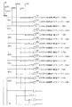
図6は、本発明の第2の実施形態における固体撮像素子50の等価回路図である。本実施形態は、請求項1、請求項2、請求項6、請求項7に対応する。なお、図中の一部の要素の符号の最後には、配置行を示す1、2、3、4、5を付し、配置列との対応関係を示すa、b、c、dを付した。『配置列との対応関係』は、第1の実施形態と同様である。行や列の区別が不要な場合、符号の最後の1、2、a、b等は、適宜省略する。
FIG. 6 is an equivalent circuit diagram of the solid-state imaging device 50 according to the second embodiment of the present invention. This embodiment corresponds to
図に示すように、固体撮像素子50は、ベイヤー配列された赤画素R、緑画素G、青画素Bと、垂直走査回路60と、行毎に各画素を垂直走査回路60に接続するナンドゲートNa及びアンドゲートAnと、各画素列毎に配置された垂直信号線VSLと、垂直信号線VSLの一端側に接続された定電流源CSと、垂直信号線VSLの他端側に配置された緑水平信号線70と、赤青水平信号線72と、水平走査回路78とを有している。
As shown in the figure, a solid-state imaging device 50 includes a red pixel R, a green pixel G, and a blue pixel B arranged in a Bayer array, a
さらに、緑水平信号線70、赤青水平信号線72における出力端には、出力バッファアンプ32、34と、出力端子Gout、R/Boutと、水平リセットトランジスタTRg、TRrbとがそれぞれ接続されている。なお、奇数行の1列目には画素は配置されない。また、図では煩雑となるので画素数を5×4として記載したが、実際にはもっと多くの画素が配列される。
Further,
第2の実施形態と第1の実施形態との主な違いは、本実施形態では画素の列間の垂直信号線が1本であることと、各垂直信号線VSLの他端を緑水平信号線70または赤青水平信号線72に接続する回路構成である。
本実施形態では、各垂直信号線VSLの他端は2つに分岐しており、分岐した双方はどちらも、別々に配置された同様の回路により同じ水平信号線(緑水平信号線70、赤青水平信号線72のいずれか)に接続されている。そして、緑水平信号線70に接続される垂直信号線(VSLa、VSLc)と、赤青水平信号線72に接続される垂直信号線(VSLb、VSLd)とは、列順次に交互に配置される。
The main difference between the second embodiment and the first embodiment is that in this embodiment, there is one vertical signal line between pixel columns, and the other end of each vertical signal line VSL is connected to a green horizontal signal. The circuit configuration is connected to the line 70 or the red / blue horizontal signal line 72.
In this embodiment, the other end of each vertical signal line VSL is branched into two, and both of the branched branches are the same horizontal signal line (green horizontal signal line 70, red) by a similar circuit arranged separately. One of the blue horizontal signal lines 72). The vertical signal lines (VSLa, VSLc) connected to the green horizontal signal line 70 and the vertical signal lines (VSLb, VSLd) connected to the red / blue horizontal signal line 72 are alternately arranged in a column sequence. .
垂直信号線VSLの他端において、分岐した一方は、XY選択トランジスタQx、nチャネルデプレッション型MOSトランジスタである中継トランジスタDx、CDSコンデンサCx、列選択トランジスタThxを介して緑水平信号線70または赤青水平信号線72に接続されている。分岐した他方は、XY選択トランジスタQy、nチャネルデプレッション型MOSトランジスタである中継トランジスタDy、CDSコンデンサCy、列選択トランジスタThyを介して、分岐した一方と同じ水平信号線(緑水平信号線70または赤青水平信号線72)に接続されている。ここでは区別し易くする為に、分岐した一方(図では垂直走査回路60側)に対応する要素の符合には文字xを含め、他方には文字yを含めた。
One of the branches at the other end of the vertical signal line VSL is an XY selection transistor Qx, a relay transistor Dx which is an n-channel depletion type MOS transistor, a CDS capacitor Cx, a column selection transistor Thx, and the green horizontal signal line 70 or red-blue. It is connected to the horizontal signal line 72. The other branched side passes through the XY selection transistor Qy, the relay transistor Dy that is an n-channel depletion type MOS transistor, the CDS capacitor Cy, and the column selection transistor Thy, and the same horizontal signal line (green horizontal signal line 70 or red) as the branched one. It is connected to the blue horizontal signal line 72). Here, for easy identification, the letter x is included in the sign of the element corresponding to one of the branches (on the
XY選択トランジスタQxは、駆動電圧φSHVxを全列共通にゲートに受け、XY選択トランジスタQyは、駆動電圧φSHVyを全列共通にゲートに受ける。各中継トランジスタDx(Dy)は、ソースが別々の定電流源Zx(Zy)を介して接地線GNDに接続されており、ドレインが電源線VCCに接続されている。なお、図では煩雑となるので、定電流源Zx、Zyに対しては一部にのみ符合を示した。 The XY selection transistor Qx receives the drive voltage φSHVx at the gate common to all columns, and the XY selection transistor Qy receives the drive voltage φSHVy at the gate common to all columns. Each relay transistor Dx (Dy) has a source connected to the ground line GND via a separate constant current source Zx (Zy), and a drain connected to the power supply line VCC. In addition, since it becomes complicated in the drawing, only a part of the constant current sources Zx and Zy is indicated.
また、各垂直信号線VSLの他端において、分岐した一方にはCDSコンデンサCxと共に相関二重サンプリング処理を行うCDSトランジスタTxが接続されており、他方にはCDSコンデンサCyと共に相関二重サンプリング処理を行うCDSトランジスタTyが接続されている。CDSトランジスタTxは、FPN蓄積パルスφcxを全列共通にゲートに受け、導通または非導通状態に切り替わる。CDSトランジスタTyは、FPN蓄積パルスφcyを全列共通にゲートに受け、導通または非導通状態に切り替わる。 Further, at the other end of each vertical signal line VSL, one of the branches is connected to a CDS transistor Tx that performs correlated double sampling processing together with the CDS capacitor Cx, and the other is subjected to correlated double sampling processing together with the CDS capacitor Cy. A CDS transistor Ty to be performed is connected. The CDS transistor Tx receives the FPN accumulation pulse φcx at the gate in common for all the columns, and switches to the conductive or nonconductive state. The CDS transistor Ty receives the FPN accumulation pulse φcy at the gate in common for all columns, and switches to a conductive or non-conductive state.
各列選択トランジスタThx、Thyのゲートは、2つの画素列毎に共通となる駆動電圧φGHを水平走査回路78から受け、導通または非導通状態に切り替わる。従って、列選択トランジスタThx、ThyやXY選択トランジスタQx、Qyが全て導通状態であれば、請求項記載のように、複数の容量(CDSコンデンサCx、Cy)が並列接続されていることと等価である。
The gates of the column selection transistors Thx and Thy receive the driving voltage φGH common to the two pixel columns from the
図7は、図6における垂直走査回路60と各画素との接続部分に着目した回路図である。垂直走査回路60は、第1の実施形態と同様に各画素行に対して1本の出力信号線を有し、これら出力信号線は、垂直走査回路60からの行選択信号OPT1〜OPTnをそれぞれ受ける。ナンドゲートNa及びアンドゲートAnは、一方の入力端子に行選択信号OPTを受ける点では第1の実施形態と同様であるが、他方の入力端子への入力電圧が異なる。
FIG. 7 is a circuit diagram focusing on the connection between the
即ち、各行において、駆動電圧φTG1、φTG2のどちらがナンドゲートNaの他方の入力端子に入力され、駆動電圧φRSG1、φRSG2のどちらがアンドゲートAnの他方の入力端子に入力されるかが異なる。具体的には、(4n−3)行目、(4n−2)行目では、ナンドゲートNaの他方の入力端子は駆動電圧φTG1を受け、アンドゲートAnの他方の入力端子は駆動電圧φRSG1を受ける。反対に、(4n−1)行目、4n行目では、ナンドゲートNaの他方の入力端子は駆動電圧φTG2を受け、アンドゲートAnの他方の入力端子は駆動電圧φRSG2を受ける。 That is, in each row, which of the drive voltages φTG1 and φTG2 is input to the other input terminal of the NAND gate Na and which of the drive voltages φRSG1 and φRSG2 is input to the other input terminal of the AND gate An is different. Specifically, in the (4n-3) th and (4n-2) th rows, the other input terminal of the NAND gate Na receives the drive voltage φTG1, and the other input terminal of the AND gate An receives the drive voltage φRSG1. . On the other hand, in the (4n-1) th row and the 4nth row, the other input terminal of the NAND gate Na receives the drive voltage φTG2, and the other input terminal of the AND gate An receives the drive voltage φRSG2.
以上の回路構成において、請求項との対応関係は、例えば以下の通りである。
請求項記載の一対の容量は、CDSコンデンサCx、Cyに対応する。請求項記載の垂直信号線Aは、垂直信号線VSLa、VSLcに対応する。請求項記載の垂直信号線Bは、垂直信号線VSLb、VSLdに対応する。請求項記載のスイッチング回路は、XY選択トランジスタQx、Qy、中継トランジスタDx、Dy、定電流源Zx、Zy、CDSトランジスタTx、Ty、列選択トランジスタThx、Thy、水平リセットトランジスタTRg、TRrb、水平走査回路78に対応する。その他の要素の対応関係は、第1の実施形態と同様である。
In the above circuit configuration, the correspondence with the claims is, for example, as follows.
The pair of capacitances recited in the claims corresponds to the CDS capacitors Cx and Cy. The vertical signal line A described in the claims corresponds to the vertical signal lines VSLa and VSLac. The vertical signal line B described in the claims corresponds to the vertical signal lines VSLb and VSLd. The switching circuit according to the present invention includes XY selection transistors Qx and Qy, relay transistors Dx and Dy, constant current sources Zx and Zy, CDS transistors Tx and Ty, column selection transistors Thx and Thy, horizontal reset transistors TRg and TRrb, horizontal scanning This corresponds to the
図8は、上述の固体撮像素子50において通常読み出しを行う場合の各部の電圧波形を示すタイミング図である。以下、図6及び図8を参照しながら回路動作を説明する。なお、読み出し走査は4行単位で同じになる。各行の読み出し走査の主な違いは、(4n−3)行目及び(4n−2)行目では駆動電圧φRSG1、φTG1を用い、(4n−1)行目及び4n行目では駆動電圧φRSG2、φTG2を用いることである。 FIG. 8 is a timing chart showing voltage waveforms at various parts when normal reading is performed in the solid-state imaging device 50 described above. The circuit operation will be described below with reference to FIGS. Note that readout scanning is the same in units of four rows. The main difference in readout scanning of each row is that the driving voltages φRSG1 and φTG1 are used in the (4n-3) th and (4n-2) th rows, and the driving voltage φRSG2 is used in the (4n-1) th and 4nth rows. φTG2 is used.
まず、第1の実施形態と同様に、スタートパルスSTV、クロック信号CLKV1、CLKV2を垂直走査回路60に入力する。これにより、垂直走査回路60が出力する行選択信号はOPT1のみが高レベルとなり、1行目が選択される。なお、クロック信号CLKV1、CLKV2の入力直後では、第1の実施形態と同様に、全画素において、転送ゲートFWはオフ状態であり、JFETのゲート電圧はリセットされている(2行目以降の選択直後も同様)。
First, as in the first embodiment, a start pulse STV and clock signals CLKV1, CLKV2 are input to the
次に、駆動電圧φRSG1、φSHVx、φSHVyを同時に高レベルに切り替える。これにより、1行目では、アンドゲートAn1の出力電圧は高レベルに切り替わり、リセットゲートRGはオフし、JFETのゲートはフローティング状態になる。また、全列のXY選択トランジスタQx、Qyはオンする。
次に、FPN蓄積パルスφcx、φcyを同時に高レベルに切り替え、全てのCDSトランジスタTx、Tyをオンし、CDSコンデンサCx、Cyにおける一方の電極を定電圧源Vrefに接続する。このときはまだ、JFETのゲートにはフォトダイオードPDの信号電荷が転送されておらず、固定パターンノイズ成分に相当する電圧がJFETのソースから出力され、この電圧が中継トランジスタDx、Dyのゲートに印加される。これにより、中継トランジスタDx、Dyのソース電圧は、そのゲート電圧に応じたものとなり、CDSコンデンサCx、Cyは、固定パターンノイズ成分に相当する電圧に充電される。この後、FPN蓄積パルスφcx、φcyを同時に低レベルに切り替える。
Next, the drive voltages φRSG1, φSHVx, φSHVy are simultaneously switched to a high level. As a result, in the first row, the output voltage of the AND gate An1 is switched to the high level, the reset gate RG is turned off, and the gate of the JFET is in a floating state. Further, the XY selection transistors Qx and Qy in all columns are turned on.
Next, the FPN accumulation pulses φcx and φcy are simultaneously switched to a high level, all the CDS transistors Tx and Ty are turned on, and one electrode of the CDS capacitors Cx and Cy is connected to the constant voltage source Vref. At this time, the signal charge of the photodiode PD is not yet transferred to the gate of the JFET, and a voltage corresponding to the fixed pattern noise component is output from the source of the JFET, and this voltage is output to the gates of the relay transistors Dx and Dy. Applied. As a result, the source voltages of the relay transistors Dx and Dy are in accordance with the gate voltages, and the CDS capacitors Cx and Cy are charged to a voltage corresponding to the fixed pattern noise component. Thereafter, the FPN accumulation pulses φcx and φcy are simultaneously switched to a low level.
次に、駆動電圧φTG1を高レベルに切り替える。これにより、1行目では、ナンドゲートNa1の出力電圧が低レベルに切り替わって転送ゲートFWがオンし、フォトダイオードPDの信号電荷はJFETのゲートに転送される。JFETは、ゲート内の蓄積電荷量に応じた信号電圧(画素信号)をソースから出力する。これにより、CDSコンデンサCx、Cyには、中継トランジスタDx、Dyを介して、先に充電した固定パターンノイズ成分が相殺されるように画素信号が充電される。 Next, the drive voltage φTG1 is switched to a high level. Thereby, in the first row, the output voltage of the NAND gate Na1 is switched to a low level, the transfer gate FW is turned on, and the signal charge of the photodiode PD is transferred to the gate of the JFET. The JFET outputs a signal voltage (pixel signal) corresponding to the amount of charge accumulated in the gate from the source. As a result, the pixel signals are charged in the CDS capacitors Cx and Cy through the relay transistors Dx and Dy so that the fixed pattern noise component charged earlier is canceled out.
なお、XY選択トランジスタQx、Qyはスレッショルド電圧等のパラメータが互いに同じ素子であり、中継トランジスタDx、Dyも互いに同じ素子である。従って、通常読み出しでは、CDSコンデンサCx、Cyはどちらも同じ電圧に充電される(2行目以降も同様)。即ち、1行目における2、4列目の緑画素Gの画素信号は、それぞれ、a、c列のCDSコンデンサCx、Cyに等しく充電され、1行目における3、5列目の赤画素Rの画素信号は、それぞれ、b、d列のCDSコンデンサCx、Cyに等しく充電される。この後、駆動電圧φTG1は低レベルに切り替わる。 The XY selection transistors Qx and Qy are elements having the same parameters such as the threshold voltage, and the relay transistors Dx and Dy are also elements having the same parameters. Therefore, in normal reading, the CDS capacitors Cx and Cy are both charged to the same voltage (the same applies to the second and subsequent rows). That is, the pixel signals of the green pixels G in the second and fourth columns in the first row are charged equally to the CDS capacitors Cx and Cy in the a and c columns, respectively, and the red pixels R in the third and fifth columns in the first row. Are charged equally to the CDS capacitors Cx and Cy in the b and d columns, respectively. Thereafter, the drive voltage φTG1 is switched to a low level.
次に、駆動電圧φRSG1、φSHVx、φSHVyを同時に低レベルに切り替える。これにより、1行目の転送ゲートFWはオフし、全列のXY選択トランジスタQx、Qyはオフする。さらに、全列の中継トランジスタDx、Dyは、ゲートがフローティング状態になるが、MOSトランジスタであるのでφTG1が高レベルの期間にゲートに蓄積した電荷を保持し、ソース電圧が変わらない。この状態で、緑水平信号線70及び赤青水平信号線72の電圧をVrefにリセットする動作と、水平走査回路78の水平シフトレジスタを順送りにオンする動作とを繰り返し、1行目の画素信号を水平方向に読み出す。
Next, the drive voltages φRSG1, φSHVx, φSHVy are simultaneously switched to a low level. As a result, the transfer gate FW in the first row is turned off, and the XY selection transistors Qx and Qy in all the columns are turned off. Further, the relay transistors Dx and Dy of all the columns have the gates in a floating state, but are MOS transistors, so that the charges accumulated in the gates during the period in which φTG1 is at a high level are held, and the source voltage does not change. In this state, the operation of resetting the voltages of the green horizontal signal line 70 and the red-blue horizontal signal line 72 to Vref and the operation of turning on the horizontal shift register of the
具体的にはまず、水平リセットパルス電圧φRSTHを高レベルに切り替える。これにより、水平リセットトランジスタTRg、TRrbはオンして、緑水平信号線70及び赤青水平信号線72の電圧はVrefにリセットされる。この後、水平リセットパルス電圧φRSTHを低レベルに切り替える。
次に、水平走査回路78は、a、b列に対応する駆動電圧φGHabを高レベルに切り替える。これにより、列選択トランジスタThxa、Thya、Thxb、Thybをオンして、a列のCDSコンデンサCxa、Cyaに充電した画素信号を緑水平信号線70に読み出し、b列のCDSコンデンサCxb、Cybに充電した画素信号を赤青水平信号線72に読み出す。
Specifically, first, the horizontal reset pulse voltage φRSTH is switched to a high level. As a result, the horizontal reset transistors TRg and TRrb are turned on, and the voltages of the green horizontal signal line 70 and the red / blue horizontal signal line 72 are reset to Vref. Thereafter, the horizontal reset pulse voltage φRSTH is switched to a low level.
Next, the
ここで、緑水平信号線70に出力される信号電圧は、その寄生容量を考慮すれば、第1の実施形態の通常読み出しの場合と同様になる。即ち、JFETのソースの出力電圧値をJS、CDSコンデンサCx、Cyの容量値をそれぞれCFx、CFy、緑水平信号線70の寄生容量値をCFG、緑水平信号線70の出力電圧をVgreenとすれば、次式のようになる。
Vgreen=JS×(CFx+CFy)/(CFx+CFy+CFG)・・・(4)
赤青水平信号線72の出力電圧も同様になる。なお、本実施形態では一例として、CFx=CFyである。
Here, the signal voltage output to the green horizontal signal line 70 is the same as that in the normal reading in the first embodiment in consideration of the parasitic capacitance. That is, the output voltage value of the JFET source is JS, the capacitance values of the CDS capacitors Cx and Cy are CFx and CFy, the parasitic capacitance value of the green horizontal signal line 70 is CFG, and the output voltage of the green horizontal signal line 70 is Vgreen. For example, the following equation is obtained.
Vgreen = JS × (CFx + CFy) / (CFx + CFy + CFG) (4)
The output voltage of the red / blue horizontal signal line 72 is the same. In the present embodiment, as an example, CFx = CFy.
ここまでが1行目における2、3列目の画素信号の読み出しである。次に、水平リセットパルス電圧φRSTHを高レベルに切り替えて、緑水平信号線70及び赤青水平信号線72の電圧をリセット後、水平リセットパルス電圧φRSTHを低レベルに切り替える。そして、c、d列に対応する駆動電圧φGHcdを高レベルに切り替え、4、5列目の画素信号を同様に読み出す。このような動作を繰り返すことにより、1行目の画素信号の読み出しを2列毎に行う。ここまでが図8における『1行目選択期間』の期間である。 This is the reading of the pixel signals in the second and third columns in the first row. Next, the horizontal reset pulse voltage φRSTH is switched to a high level, the voltages of the green horizontal signal line 70 and the red-blue horizontal signal line 72 are reset, and then the horizontal reset pulse voltage φRSTH is switched to a low level. Then, the drive voltage φGHcd corresponding to the c and d columns is switched to a high level, and the pixel signals in the fourth and fifth columns are similarly read out. By repeating such an operation, the pixel signal in the first row is read every two columns. This is the “first row selection period” in FIG.
次に、クロック信号CLKV1、CLKV2を垂直走査回路60に入力して2行目を選択後、駆動電圧φRSG1、φSHVx、φSHVyを高レベルに切り替える。この後、1行目の場合と同様に、FPN蓄積パルスφcx、φcyを同時に高レベルに切り替えることでCDSコンデンサCx、Cyに固定パターンノイズ成分を充電後、FPN蓄積パルスφcx、φcyを同時に低レベルに切り替える。
Next, after the clock signals CLKV1 and CLKV2 are input to the
次に、駆動電圧φTG1を高レベルに切り替える。これにより、2行目では、ナンドゲートNa2の出力電圧が低レベルに切り替わって転送ゲートFWがオンし、フォトダイオードPDの信号電荷はJFETのゲートに転送される。これにより、2行目における1、3列目の緑画素Gの画素信号は、それぞれ、a、c列のCDSコンデンサCx、Cyに充電される。2行目における2、4列目の青画素Bの画素信号は、それぞれ、b、d列のCDSコンデンサCx、Cyに充電される。 Next, the drive voltage φTG1 is switched to a high level. Thus, in the second row, the output voltage of the NAND gate Na2 is switched to a low level, the transfer gate FW is turned on, and the signal charge of the photodiode PD is transferred to the gate of the JFET. Accordingly, the pixel signals of the green pixels G in the first and third columns in the second row are charged in the CDS capacitors Cx and Cy in the a and c columns, respectively. The pixel signals of the blue pixels B in the second and second columns in the second row are charged in the CDS capacitors Cx and Cy in the b and d columns, respectively.
次に、駆動電圧φRSG1、φSHVx、φSHVyを低レベルに切り替え、全列のXY選択トランジスタQx、Qyをオフする。そして、1行目の場合と同様に、2行目の画素信号の水平読み出しを2列毎に行う。
次に、クロック信号CLKV1、CLKV2を垂直走査回路60に入力し、3行目を選択後、駆動電圧φRSG2、φSHVx、φSHVyを同時に高レベルに切り替える。この後、1、2行目と同様に、FPN蓄積パルスφcx、φcyを高レベルに切り替えて、CDSコンデンサCx、Cyに固定パターンノイズ成分を充電後、FPN蓄積パルスφcx、φcyを低レベルに切り替える。
Next, the drive voltages φRSG1, φSHVx, φSHVy are switched to a low level, and the XY selection transistors Qx, Qy of all the columns are turned off. Then, as in the case of the first row, horizontal readout of the pixel signals of the second row is performed every two columns.
Next, the clock signals CLKV1 and CLKV2 are input to the
次に、駆動電圧φTG2を高レベルに切り替え、3行目における2〜5列目の画素信号を、それぞれ、a〜d列のCDSコンデンサCx、Cyに充電する。次に、駆動電圧φRSG2、φSHVx、φSHVyを低レベルに切り替え、全列のXY選択トランジスタQx、Qyをオフした後、前述と同様に3行目の画素信号を水平方向に読み出す。
次に、クロック信号CLKV1、CLKV2を垂直走査回路60に入力して4行目を選択後、駆動電圧φRSG2、φSHVx、φSHVyを高レベルに切り替える。この後、FPN蓄積パルスφcx、φcyを高レベルに切り替え、CDSコンデンサCx、Cyに固定パターンノイズ成分を充電後、FPN蓄積パルスφcx、φcyを低レベルに切り替える。
Next, the drive voltage φTG2 is switched to a high level, and the pixel signals in the second to fifth columns in the third row are charged in the CDS capacitors Cx and Cy in the a to d columns, respectively. Next, the drive voltages φRSG2, φSHVx, φSHVy are switched to a low level, the XY selection transistors Qx, Qy of all the columns are turned off, and then the pixel signals in the third row are read in the horizontal direction in the same manner as described above.
Next, after the clock signals CLKV1 and CLKV2 are input to the
次に、駆動電圧φTG2を高レベルに切り替え、4行目における1〜4列目の画素信号を、それぞれ、a〜d列のCDSコンデンサCx、Cyに充電する。次に、駆動電圧φRSG2、φSHVx、φSHVyを低レベルに切り替えた後、4行目の画素信号を前述と同様に水平方向に読み出す。以上の動作を繰り返して、5行目以降の画素信号も同様に読み出す。以上が通常読み出しの動作説明である。 Next, the drive voltage φTG2 is switched to a high level, and the pixel signals in the first to fourth columns in the fourth row are charged in the CDS capacitors Cx and Cy in the a to d columns, respectively. Next, after the drive voltages φRSG2, φSHVx, and φSHVy are switched to a low level, the pixel signals in the fourth row are read out in the horizontal direction in the same manner as described above. By repeating the above operation, the pixel signals in the fifth and subsequent rows are similarly read out. The above is the description of the normal reading operation.
図9は、固体撮像素子50において間引き読み出しを行う場合の各部の電圧波形を示すタイミング図である。以下、図6及び図9を参照しながら間引き読み出しの動作を説明する。この場合も、読み出し走査は4行単位で同じになる。
まず、第1の実施形態の間引き読み出しの場合と同様の手順で、スタートパルスSTV、クロック信号CLKV1、CLKV2を垂直走査回路60に入力し、1行目と3行目を同時に選択する。
FIG. 9 is a timing chart showing voltage waveforms at various parts when thinning readout is performed in the solid-state imaging device 50. Hereinafter, the thinning-out reading operation will be described with reference to FIGS. Also in this case, readout scanning is the same in units of four rows.
First, the start pulse STV and the clock signals CLKV1 and CLKV2 are input to the
次に、駆動電圧φRSG1、φSHVxを同時に高レベルに切り替える。これにより、1行目のJFETのゲートはフローティング状態になり、全列のXY選択トランジスタの内、一方であるQxのみがオンする。即ち、選択されている3行目のアンドゲートAn3は、駆動電圧φRSG1ではなく駆動電圧φRSG2を受けるものなので、3行目のJFETはリセットされたままである。 Next, the drive voltages φRSG1 and φSHVx are simultaneously switched to a high level. As a result, the gates of the JFETs in the first row are in a floating state, and only one Qx of the XY selection transistors in all the columns is turned on. That is, since the selected AND gate An3 in the third row receives the drive voltage φRSG2 instead of the drive voltage φRSG1, the JFET in the third row remains reset.
次に、FPN蓄積パルスφcxを高レベルに切り替える。これにより、全列のCDSトランジスタの内、一方であるTxのみがオンし、CDSコンデンサCxには、固定パターンノイズ成分が充電される。この後、FPN蓄積パルスφcxを低レベルに切り替える。
次に、駆動電圧φTG1を高レベルに切り替える。これにより、1行目では、フォトダイオードPDの信号電荷はJFETのゲートに転送され、CDSコンデンサCxにはそれぞれ、1行目の各列の画素信号が充電される。次に、駆動電圧φTG1を低レベルに切り替えてから、駆動電圧φRSG1、φSHVxを同時に低レベルに切り替える。これにより、1行目の転送ゲートFWはオフし、1行目のJFETのゲートはリセットされ、XY選択トランジスタQxはオフする。
Next, the FPN accumulation pulse φcx is switched to a high level. As a result, only one Tx of the CDS transistors in all the columns is turned on, and the CDS capacitor Cx is charged with a fixed pattern noise component. Thereafter, the FPN accumulation pulse φcx is switched to a low level.
Next, the drive voltage φTG1 is switched to a high level. Thereby, in the first row, the signal charge of the photodiode PD is transferred to the gate of the JFET, and the CDS capacitor Cx is charged with the pixel signal in each column of the first row. Next, after the drive voltage φTG1 is switched to a low level, the drive voltages φRSG1 and φSHVx are simultaneously switched to a low level. Thereby, the transfer gate FW in the first row is turned off, the gate of the JFET in the first row is reset, and the XY selection transistor Qx is turned off.
次に、駆動電圧φRSG2、φSHVyを同時に高レベルに切り替える。これにより、3行目のJFETのゲートはフローティング状態になり、全列のXY選択トランジスタの内、一方であるQyのみがオンする。なお、1行目のJFETはリセットされたままである。次に、FPN蓄積パルスφcyを高レベルに切り替える。これにより、全列のCDSトランジスタの内、一方であるTyのみがオンし、CDSコンデンサCyには、固定パターンノイズ成分が充電される。この後、FPN蓄積パルスφcyを低レベルに切り替える。 Next, the drive voltages φRSG2 and φSHVy are simultaneously switched to a high level. As a result, the gates of the JFETs in the third row are in a floating state, and only one Qy of the XY selection transistors in all the columns is turned on. Note that the JFET in the first row remains reset. Next, the FPN accumulation pulse φcy is switched to a high level. As a result, only one Ty of the CDS transistors in all the columns is turned on, and the CDS capacitor Cy is charged with a fixed pattern noise component. Thereafter, the FPN accumulation pulse φcy is switched to a low level.
次に、駆動電圧φTG2を高レベルに切り替える。これにより、3行目では、フォトダイオードPDの信号電荷はJFETのゲートに転送され、CDSコンデンサCyにはそれぞれ、3行目の各列の画素信号が充電される。次に、駆動電圧φTG2を低レベルに切り替えてから、駆動電圧φRSG2、φSHVyを同時に低レベルに切り替える。これにより、3行目の転送ゲートFWはオフし、3行目のJFETのゲートはリセットされ、XY選択トランジスタQyはオフする。また、中継トランジスタDx、Dyは、MOSトランジスタであるので、XY選択トランジスタQx、Qyがオフする直前と同じ電圧(信号電圧)をソースから出力し続ける。この状態で、通常読み出しの場合と同様に、水平方向に画素信号を読み出す。 Next, the drive voltage φTG2 is switched to a high level. As a result, in the third row, the signal charge of the photodiode PD is transferred to the gate of the JFET, and the CDS capacitor Cy is charged with the pixel signal in each column of the third row. Next, after the drive voltage φTG2 is switched to a low level, the drive voltages φRSG2 and φSHVy are simultaneously switched to a low level. As a result, the transfer gate FW in the third row is turned off, the gate of the JFET in the third row is reset, and the XY selection transistor Qy is turned off. Since the relay transistors Dx and Dy are MOS transistors, the same voltage (signal voltage) as that immediately before the XY selection transistors Qx and Qy are turned off is continuously output from the source. In this state, the pixel signal is read out in the horizontal direction as in the case of normal reading.
但し、CDSコンデンサCxには1行目の画素信号が充電されており、CDSコンデンサCyには3行目の画素信号が充電されているので、緑水平信号線70の出力電圧は、第1の実施形態の間引き読み出しと同様に、合算平均されたものとなる。従って、1行目のJFETのソースの出力電圧値をJS1、3行目のJFETのソースの出力電圧値をJS3とすれば、緑水平信号線70の出力電圧Vgreenは、次式のようになる。
Vgreen=(JS1×CFx+JS3×CFy)/(CFx+CFy+CFH)
・・・(5)
赤青水平信号線72の出力電圧も同様である。ここまでが図9における『1、3行目水平読み出し』の期間である。
However, since the CDS capacitor Cx is charged with the pixel signal of the first row and the CDS capacitor Cy is charged with the pixel signal of the third row, the output voltage of the green horizontal signal line 70 is the first voltage. Similar to the thinning-out readout of the embodiment, the sum is averaged. Accordingly, if the output voltage value of the source of the JFET in the first row is JS1, and the output voltage value of the source of the JFET in the third row is JS3, the output voltage Vgreen of the green horizontal signal line 70 is as follows: .
Vgreen = (JS1 × CFx + JS3 × CFy) / (CFx + CFy + CFH)
... (5)
The same applies to the output voltage of the red / blue horizontal signal line 72. This is the period of “1, 3rd row horizontal readout” in FIG.
次に、クロック信号CLKV1、CLKV2を1パルスずつ垂直走査回路8に入力し、垂直シフトレジスタを1つシフトさせ、2行目と4行目を同時に選択する。次に、駆動電圧φRSG2、φSHVx、φSHVyを同時に高レベルに切り替える。これにより、4行目のJFETのゲートはフローティング状態になり、全列のXY選択トランジスタQx、Qyはオンする。なお、2行目も選択されているが、2行目のアンドゲートAn2は駆動電圧φRSG2ではなくφRSG1を受けるものなので、2行目のJFETはリセットされたままである。 Next, the clock signals CLKV1 and CLKV2 are input to the vertical scanning circuit 8 one pulse at a time, the vertical shift register is shifted by one, and the second and fourth rows are selected simultaneously. Next, the drive voltages φRSG2, φSHVx, φSHVy are simultaneously switched to a high level. As a result, the gates of the JFETs in the fourth row are in a floating state, and the XY selection transistors Qx and Qy in all the columns are turned on. Although the second row is also selected, since the AND gate An2 in the second row receives φRSG1 instead of the drive voltage φRSG2, the JFET in the second row remains reset.
次に、FPN蓄積パルスφcx、φcyを同時に高レベルに切り替える。これにより、CDSコンデンサCx、Cyには、4行目の各画素の固定パターンノイズ成分が充電される。即ち、第1の実施形態の間引き読み出しと同様に、2行目は選択されているが、その画素信号は読み出されず、CDSコンデンサCx、Cyの充電電圧は列毎に同じになる。この後、FPN蓄積パルスφcx、φcyを低レベルに切り替える。次に、駆動電圧φTG2を高レベルに切り替える。これにより、CDSコンデンサCx、Cyにはそれぞれ、4行目の各列の画素信号が充電される。次に、駆動電圧φTG2を低レベルに切り替えてから、駆動電圧φRSG2、φSHVx、φSHVyを低レベルに切り替えた後、通常読み出しの場合と同様に、4行目の画素信号を水平方向に読み出す。 Next, the FPN accumulation pulses φcx and φcy are simultaneously switched to a high level. As a result, the CDS capacitors Cx and Cy are charged with the fixed pattern noise component of each pixel in the fourth row. That is, as with the thinning readout in the first embodiment, the second row is selected, but the pixel signal is not read out, and the charging voltages of the CDS capacitors Cx and Cy are the same for each column. Thereafter, the FPN accumulation pulses φcx and φcy are switched to a low level. Next, the drive voltage φTG2 is switched to a high level. Thereby, the CDS capacitors Cx and Cy are charged with the pixel signals of the respective columns in the fourth row. Next, after the drive voltage φTG2 is switched to a low level and the drive voltages φRSG2, φSHVx, and φSHVy are switched to a low level, the pixel signals in the fourth row are read in the horizontal direction in the same manner as in the normal reading.
次に、クロック信号CLKV1、CLKV2を3パルスずつ垂直走査回路60に入力し、垂直シフトレジスタを3つシフトさせ、5行目と7行目を同時に選択する。この後、1、3行目の場合と同様の走査により、5行目と7行目の画素信号を合算平均して読み出す。
次に、クロック信号CLKV1、CLKV2を1パルスずつ垂直走査回路60に入力し、垂直シフトレジスタを1つシフトさせ、6行目と8行目を同時に選択する。この後、4行目の場合と同様の走査により、8行目の画素信号を単独で読み出す。以上の動作を繰り返して、9行目以降の画素信号も同様に読み出す。即ち、(4n−3)行目と(4n−1)行目の画素信号を混合読み出しした後、4n行目の画素信号を単独で読み出す動作を繰り返す。以上が間引き読み出しの動作説明である。
Next, the clock signals CLKV1 and CLKV2 are inputted to the
Next, the clock signals CLKV1 and CLKV2 are input to the
このように第2の実施形態においても、各画素の画素信号は、まずJFETのソース電圧として読み出され、緑水平信号線70、赤青水平信号線72には電圧として出力される。そして、本実施形態の間引き読み出しにおいても、奇数行がGR行であるベイヤー配列において、第1の実施形態の間引き読み出しと同様に、(4n−3)行目と(4n−1)行目を混合読み出しする動作と、4n行目を読み出す動作とを繰り返す。従って、第1の実施形態と同様の効果が得られる。 As described above, also in the second embodiment, the pixel signal of each pixel is first read as the source voltage of the JFET, and is output as a voltage to the green horizontal signal line 70 and the red-blue horizontal signal line 72. In the thinning-out readout of the present embodiment, the (4n-3) th and (4n-1) -th rows are the same as in the thinning-out readout of the first embodiment in the Bayer array in which the odd-numbered rows are GR rows. The mixed read operation and the fourth read operation are repeated. Therefore, the same effect as the first embodiment can be obtained.
さらに、本実施形態では、画素の列間の垂直信号線は1本のみでよく、配線は容易になる。また、本実施形態では、8つの選択用駆動電圧φPαL〜φPδR、及び1つのFPN蓄積パルスφcの代わりに、駆動電圧φSHVx、φSHVy、及び2つのFPN蓄積パルスφcx、φcyを用いる。即ち、第1の実施形態よりも駆動電圧の種類は少なくなる。 Further, in the present embodiment, only one vertical signal line between the pixel columns is required, and wiring becomes easy. In the present embodiment, the drive voltages φSHVx and φSHVy and the two FPN accumulation pulses φcx and φcy are used instead of the eight selection drive voltages φPαL to φPδR and one FPN accumulation pulse φc. That is, there are fewer types of drive voltages than in the first embodiment.
なお、本実施形態の間引き読み出しでは、GR行に対しては混合読み出しを行い、GB行は単独で読み出したが、その反対にしてもよい。即ち、GR行である(4n−3)行目を単独で読み出す動作と、GB行である(4n−2)行目、4n行目を混合読み出しする動作とを順次繰り返してもよい。この場合も、サンプリング重心は等間隔になる。或いは、(4n−3)行目と(4n−1)行目の画素信号を混合読み出しする動作と、(4n−2)行目と4n行目の画素信号を混合読み出しする動作とを繰り返してもよい。この場合、サンプリング重心が等間隔にならない点を除き、上述と同様の効果が得られる。 In the thinning-out readout according to the present embodiment, mixed readout is performed on the GR row and the GB row is read out independently, but the opposite is also possible. That is, the operation of independently reading the (4n-3) th row that is the GR row and the operation of reading the mixed (4n-2) th and 4nth rows that are the GB row may be sequentially repeated. Also in this case, the sampling centroids are equally spaced. Alternatively, the operation of mixing and reading the pixel signals of the (4n-3) th row and the (4n-1) th row and the operation of reading the pixel signals of the (4n-2) th row and the 4nth row are repeated. Also good. In this case, the same effect as described above can be obtained except that the sampling centroids are not equally spaced.
垂直信号線VSLと、緑水平信号線70(または赤青水平信号線72)との間には、2つの同様の回路が並列接続されている例を述べたが、3つ以上の同様の回路を並列接続してもよい。ここでの『同様の回路』とは、XY選択トランジスタQx、中継トランジスタDx、定電流源Zx、CDSコンデンサCx、CDSトランジスタTx、列選択トランジスタThxに相当する。その場合、駆動電圧φSHVxに相当するものを、並列接続の数だけ入力すればよい。『同様の回路』を例えば4つ並列接続すれば、第1の実施形態の補足事項で述べたものと同様に、(8n−7)行目、(8n−5)行目、(8n−3)行目、(8n−1)行目を混合読み出しする動作と、8n行目を単独で読み出す動作とを繰り返すことができる。 The example in which two similar circuits are connected in parallel between the vertical signal line VSL and the green horizontal signal line 70 (or the red-blue horizontal signal line 72) has been described. However, three or more similar circuits have been described. May be connected in parallel. The “similar circuit” here corresponds to the XY selection transistor Qx, the relay transistor Dx, the constant current source Zx, the CDS capacitor Cx, the CDS transistor Tx, and the column selection transistor Thx. In that case, the number corresponding to the drive voltage φSHVx may be input by the number of parallel connections. If, for example, four “similar circuits” are connected in parallel, the (8n-7) th row, the (8n-5) th row, and (8n-3) are the same as those described in the supplementary items of the first embodiment. ) The operation of reading the mixed line and the (8n-1) th row and the operation of reading the 8nth row alone can be repeated.
また、第1及び第2の実施形態では、画素配列がベイヤー正方配列である例を述べたが、GストライプRB線順次の正方配列の場合も、本発明は適用可能である。具体的には、第2の実施形態では、偶数行の画素は、その画素と接続されている垂直信号線VSLを基準とすれば、垂直走査回路60側に配置されている。従って、第2の実施形態では、偶数行の画素と垂直信号線VSLとの接続関係を同じにしたまま、偶数行の画素を垂直信号線VSLに対して図6の右側に配置させれば、画素配列をGストライプRB線順次に変えた上で本発明を適用できる。
In the first and second embodiments, an example in which the pixel array is a Bayer square array has been described. However, the present invention is also applicable to a G stripe RB line sequential square array. Specifically, in the second embodiment, pixels in even rows are arranged on the
また、本発明は、赤、緑、青の原色系には限定されず、例えば補色系でも適用可能である。さらに本発明は、正方配列には限定されず、ハニカム配列にも適用可能である。 The present invention is not limited to the primary colors of red, green, and blue, and can be applied to, for example, a complementary color system. Furthermore, the present invention is not limited to the square arrangement, but can be applied to a honeycomb arrangement.
以上詳述したように本発明は、固体撮像素子の分野において大いに利用可能である。 As described above in detail, the present invention can be used greatly in the field of solid-state imaging devices.
2 固体撮像素子
8 垂直走査回路
20 緑水平信号線
24 赤青水平信号線
30 水平走査回路
32、34 出力バッファアンプ
50 固体撮像素子
60 垂直走査回路
70 緑水平信号線
72 赤青水平信号線
78 水平走査回路
An1〜An5 アンドゲート
B 青画素
BiL、BiR バイポーラトランジスタ
CcL、CcR、Cxa〜Cxd、Cya〜Cyd CDSコンデンサ
CSL、CSR、CSML、CSMR、CSa〜CSd、Zx〜Zy 定電流源
Dxa〜Dxd、Dya〜Dyd 中継トランジスタ
FW 転送ゲート
G 緑画素
Gout 出力端子
Iα、Iβ、Iγ、Iδ 入力信号線
JFET 接合型電界効果トランジスタ
MXG 緑用選択回路
MXR/B 赤青用選択回路
Na1〜Na5 ナンドゲート
PD フォトダイオード
QαL、QαR、QβL、QβR、QγL、QγR、QδL、QδR スイッチ
Qxa〜Qxd、Qya〜Qyd XY選択トランジスタ
R 赤画素
R/Bout 出力端子
RG リセットゲート
Tca〜Tcd、Txa〜Txd、Tya〜Tyd CDSトランジスタ
Tha〜Thd、Thxa〜Thxd、Thya〜Thyd 列選択トランジスタ
TRg、TRrb 水平リセットトランジスタ
VL、VR、VSLa〜VSLd 垂直信号線
2 Solid-state imaging device 8 Vertical scanning circuit 20 Green horizontal signal line 24 Red-blue
Claims (7)
前記画素の列に対応してそれぞれ配置されていると共に複数の前記画素に接続されており、前記画素により生成される画素信号を前記垂直方向に転送する複数の垂直転送部と、
複数の前記垂直転送部からの前記画素信号が転送される少なくとも1つの水平信号線と
を備えた固体撮像素子であって、
前記水平信号線と、複数の前記垂直転送部との間において、複数の前記垂直転送部にそれぞれ対応して、各々の前記垂直転送部当たりに複数配置された容量を有し、
複数の前記容量は、対応する前記垂直転送部と1つの前記水平信号線との間で互いに並列接続されており、前記垂直転送部からの前記画素信号を受けて充電され、
複数の前記容量を前記水平信号線に接続することで、前記水平信号線に前記画素信号を転送するスイッチング回路を有する
ことを特徴とする固体撮像素子。 A plurality of pixels arranged two-dimensionally along vertical columns and horizontal rows;
A plurality of vertical transfer units which are respectively arranged corresponding to the columns of pixels and connected to the plurality of pixels, and which transfer pixel signals generated by the pixels in the vertical direction;
A solid-state imaging device comprising: at least one horizontal signal line to which the pixel signals from a plurality of the vertical transfer units are transferred;
Between the horizontal signal line and the plurality of vertical transfer units, each having a plurality of capacitors arranged for each of the vertical transfer units corresponding to the plurality of vertical transfer units,
The plurality of capacitors are connected in parallel between the corresponding vertical transfer unit and one horizontal signal line, and are charged by receiving the pixel signal from the vertical transfer unit,
A solid-state imaging device comprising: a switching circuit that transfers the pixel signal to the horizontal signal line by connecting a plurality of the capacitors to the horizontal signal line.
前記画素の列に対応してそれぞれ配置されていると共に複数の前記画素に接続されており、前記画素により生成される画素信号を前記垂直方向に転送する複数の垂直転送部と、
複数の前記垂直転送部からの前記画素信号が転送される水平転送部と
を備えた固体撮像素子であって、
複数の前記垂直転送部に対してそれぞれ配置された一対の容量と、前記一対の容量を前記水平転送部に接続することによって前記水平転送部に前記画素信号を転送するスイッチング回路とを有し、
前記一対の容量は、対応する前記垂直転送部に対して並列接続されており、前記垂直転送部からの前記画素信号を受けて充電され、
間引き読み出しが行われる場合、前記スイッチング回路は、前記一対の容量の一方にはある行の前記画素信号を充電させ、他方には別の行の前記画素信号を充電させ、前記一対の容量にそれぞれ充電させた前記画素信号を、合算平均されるように前記水平転送部に転送する
ことを特徴とする固体撮像素子。 A plurality of pixels arranged two-dimensionally along vertical columns and horizontal rows;
A plurality of vertical transfer units which are respectively arranged corresponding to the columns of pixels and connected to the plurality of pixels, and which transfer pixel signals generated by the pixels in the vertical direction;
A solid-state imaging device comprising a horizontal transfer unit to which the pixel signals from a plurality of vertical transfer units are transferred,
A pair of capacitors arranged for each of the plurality of vertical transfer units, and a switching circuit that transfers the pixel signal to the horizontal transfer unit by connecting the pair of capacitors to the horizontal transfer unit,
The pair of capacitors are connected in parallel to the corresponding vertical transfer unit, are charged by receiving the pixel signal from the vertical transfer unit,
When thinning readout is performed, the switching circuit charges one of the pair of capacitors with the pixel signal of a certain row, and the other charges the pixel signal of another row with the pair of capacitors. The charged pixel signal is transferred to the horizontal transfer unit so as to be averaged.
複数の前記画素は、一松状またはストライプ状に配置された第1色成分画素と、前記第1色成分画素間に線順次に配置された第2色成分画素及び第3色成分画素を含み、
前記一対の容量は、前記第1色成分画素の前記画素信号が充電される第1容量対と、前記第2及び第3色成分画素の前記画素信号が充電される第2容量対のいずれかであり、
各々の前記垂直転送部は、1種類または2種類の色成分の前記画素信号を転送する第1垂直信号線及び第2垂直信号線を有し、
前記水平転送部は、第1水平信号線と、第2水平信号線とを有し、
前記スイッチング回路は、前記第1及び第2垂直信号線から、前記第1色成分画素の前記画素信号が転送されているものを選択して前記第1容量対に接続すると共に、前記第2または第3色成分画素の前記画素信号が転送されているものを選択して前記第2容量対に接続後、前記第1容量対を前記第1水平信号線に接続し、前記第2容量対を前記第2水平信号線に接続する
ことを特徴とする固体撮像素子。 The solid-state imaging device according to claim 2,
The plurality of pixels include a first color component pixel arranged in a pine or stripe shape, and a second color component pixel and a third color component pixel arranged line-sequentially between the first color component pixels. ,
The pair of capacitors is one of a first capacitor pair that charges the pixel signal of the first color component pixel and a second capacitor pair that charges the pixel signal of the second and third color component pixels. And
Each of the vertical transfer units includes a first vertical signal line and a second vertical signal line that transfer the pixel signals of one type or two types of color components,
The horizontal transfer unit includes a first horizontal signal line and a second horizontal signal line,
The switching circuit selects one of the first and second vertical signal lines to which the pixel signal of the first color component pixel is transferred and connects the selected one to the first capacitor pair. After selecting and transferring the pixel signal of the third color component pixel to the second capacitor pair, the first capacitor pair is connected to the first horizontal signal line, and the second capacitor pair is connected to the second capacitor pair. A solid-state image sensor connected to the second horizontal signal line.
前記第1垂直信号線は、(4n−3)行目及び(4n−2)行目の前記画素に接続されており、
前記第2垂直信号線は、(4n−1)行目及び4n行目の前記画素に接続されており、
間引き読み出しが行われる場合、前記スイッチング回路は、前記一対の容量の一方には前記第1垂直信号線を接続すると共に他方には前記第2垂直信号線を接続して、(4n−3)行目及び(4n−1)行目の前記画素信号を合算平均して読み出す動作と、前記第2垂直信号線を前記一対の容量に接続して、4n行目の前記画素信号を読み出す動作とを繰り返す
ことを特徴とする固体撮像素子(但し、nは自然数である)。 The solid-state imaging device according to claim 3,
The first vertical signal line is connected to the pixels in the (4n-3) th row and the (4n-2) th row,
The second vertical signal line is connected to the pixels in the (4n-1) th row and the 4nth row,
When thinning-out reading is performed, the switching circuit connects the first vertical signal line to one of the pair of capacitors and connects the second vertical signal line to the other, and (4n-3) rows. An operation of adding and averaging the pixel signals of the first and (4n-1) th rows, and an operation of reading the pixel signals of the 4nth row by connecting the second vertical signal line to the pair of capacitors. A solid-state imaging device that is repeated (where n is a natural number).
前記第1垂直信号線は、(4n−3)行目及び(4n−2)行目の前記画素に接続されており、
前記第2垂直信号線は、(4n−1)行目及び4n行目の前記画素に接続されており、
間引き読み出しが行われる場合、前記スイッチング回路は、前記第1垂直信号線を前記一対の容量に接続して、(4n−3)行目の前記画素信号を読み出す動作と、前記一対の容量の一方には前記第1垂直信号線を接続すると共に他方には前記第2垂直信号線を接続して、(4n−2)行目及び4n行目の前記画素信号を合算平均して読み出す動作とを繰り返す
ことを特徴とする固体撮像素子。 The solid-state imaging device according to claim 3,
The first vertical signal line is connected to the pixels in the (4n-3) th row and the (4n-2) th row,
The second vertical signal line is connected to the pixels in the (4n-1) th row and the 4nth row,
When thinning-out reading is performed, the switching circuit connects the first vertical signal line to the pair of capacitors, reads the pixel signal in the (4n-3) th row, and one of the pair of capacitors. The first vertical signal line is connected to the other and the second vertical signal line is connected to the other, and the pixel signals of the (4n-2) th and 4nth rows are summed and averaged and read out. A solid-state imaging device characterized by repetition.
複数の前記画素は、一松状またはストライプ状に配置された第1色成分画素と、前記第1色成分画素間に線順次に配置された第2色成分画素及び第3色成分画素を含み、
前記垂直転送部は、前記第1色成分画素に接続された垂直信号線Aと、前記第2及び第3色成分画素に接続された垂直信号線Bのいずれかであり、
複数の前記垂直信号線A及び複数の前記垂直信号線Bは、列順次に交互に配置されており、
前記一対の容量には、いずれかの前記垂直信号線Aからの前記画素信号、または、いずれかの前記垂直信号線Bからの前記画素信号のみが充電され、
前記水平転送部は、第1水平信号線と、第2水平信号線とを有し、
前記スイッチング回路は、前記垂直信号線Aからの前記画素信号が充電される前記一対の容量を前記第1水平信号線に接続し、前記垂直信号線Bからの前記画素信号が充電される前記一対の容量を前記第2水平信号線に接続する
ことを特徴とする固体撮像素子。 The solid-state imaging device according to claim 2,
The plurality of pixels include a first color component pixel arranged in a pine or stripe shape, and a second color component pixel and a third color component pixel arranged line-sequentially between the first color component pixels. ,
The vertical transfer unit is one of a vertical signal line A connected to the first color component pixel and a vertical signal line B connected to the second and third color component pixels;
The plurality of vertical signal lines A and the plurality of vertical signal lines B are alternately arranged in a column sequence,
The pair of capacitors is charged with only the pixel signal from any one of the vertical signal lines A or the pixel signal from any one of the vertical signal lines B,
The horizontal transfer unit includes a first horizontal signal line and a second horizontal signal line,
The switching circuit connects the pair of capacitors to which the pixel signal from the vertical signal line A is charged to the first horizontal signal line, and the pair to which the pixel signal from the vertical signal line B is charged. A solid-state imaging device, wherein the capacitor is connected to the second horizontal signal line.
間引き読み出しが行われる場合、前記スイッチング回路は、(4n−3)行目及び(4n−1)行目の前記画素信号が合算平均されるように読み出す動作と、4n行目の前記画素信号を読み出す動作とを繰り返すか、或いは、(4n−3)行目の前記画素信号を読み出す動作と、(4n−2)行目及び4n行目の前記画素信号が合算平均されるように読み出す動作とを繰り返す
ことを特徴とする固体撮像素子。 The solid-state imaging device according to claim 6,
When thinning-out reading is performed, the switching circuit reads out the pixel signals of the (4n-3) th row and the (4n-1) th row so that the pixel signals are summed and averaged, and the pixel signal of the 4nth row. Or an operation of reading out the pixel signals in the (4n-3) th row, and an operation of reading out the pixel signals in the (4n-2) th and 4nth rows. The solid-state image sensor characterized by repeating.
Priority Applications (1)
| Application Number | Priority Date | Filing Date | Title |
|---|---|---|---|
| JP2004254395A JP2006074367A (en) | 2004-09-01 | 2004-09-01 | Solid-state imaging device |
Applications Claiming Priority (1)
| Application Number | Priority Date | Filing Date | Title |
|---|---|---|---|
| JP2004254395A JP2006074367A (en) | 2004-09-01 | 2004-09-01 | Solid-state imaging device |
Publications (1)
| Publication Number | Publication Date |
|---|---|
| JP2006074367A true JP2006074367A (en) | 2006-03-16 |
Family
ID=36154507
Family Applications (1)
| Application Number | Title | Priority Date | Filing Date |
|---|---|---|---|
| JP2004254395A Withdrawn JP2006074367A (en) | 2004-09-01 | 2004-09-01 | Solid-state imaging device |
Country Status (1)
| Country | Link |
|---|---|
| JP (1) | JP2006074367A (en) |
Cited By (8)
| Publication number | Priority date | Publication date | Assignee | Title |
|---|---|---|---|---|
| JP2009159335A (en) * | 2007-12-26 | 2009-07-16 | Panasonic Corp | Solid-state imaging apparatus and camera |
| JP2010010896A (en) * | 2008-06-25 | 2010-01-14 | Panasonic Corp | Solid-state imaging apparatus |
| JP2010183435A (en) * | 2009-02-06 | 2010-08-19 | Toshiba Corp | Solid-state imaging apparatus |
| JP2010263526A (en) * | 2009-05-11 | 2010-11-18 | Sony Corp | Solid-state imaging apparatus, method for driving the same and electronic device |
| JP2010272985A (en) * | 2009-05-19 | 2010-12-02 | Canon Inc | Solid-state image pickup device |
| CN102148943A (en) * | 2010-02-08 | 2011-08-10 | 佳能株式会社 | Solid-state image sensor and imaging apparatus |
| EP2309541A3 (en) * | 2009-10-06 | 2013-04-17 | Canon Kabushiki Kaisha | Solid-state image sensor and image sensing apparatus |
| JP2014131356A (en) * | 2014-03-27 | 2014-07-10 | Canon Inc | Solid state image pickup device |
-
2004
- 2004-09-01 JP JP2004254395A patent/JP2006074367A/en not_active Withdrawn
Cited By (16)
| Publication number | Priority date | Publication date | Assignee | Title |
|---|---|---|---|---|
| US8363133B2 (en) | 2007-12-26 | 2013-01-29 | Panasonic Corporation | Solid-state image capturing device and camera |
| WO2009090719A1 (en) * | 2007-12-26 | 2009-07-23 | Panasonic Corporation | Solid-state image capturing device and camera |
| JP2009159335A (en) * | 2007-12-26 | 2009-07-16 | Panasonic Corp | Solid-state imaging apparatus and camera |
| JP2010010896A (en) * | 2008-06-25 | 2010-01-14 | Panasonic Corp | Solid-state imaging apparatus |
| US8711262B2 (en) | 2009-02-06 | 2014-04-29 | Kabushiki Kaisha Toshiba | Solid-state image sensing device and control method of solid-state image sensing device |
| JP2010183435A (en) * | 2009-02-06 | 2010-08-19 | Toshiba Corp | Solid-state imaging apparatus |
| JP2010263526A (en) * | 2009-05-11 | 2010-11-18 | Sony Corp | Solid-state imaging apparatus, method for driving the same and electronic device |
| JP2010272985A (en) * | 2009-05-19 | 2010-12-02 | Canon Inc | Solid-state image pickup device |
| US8451360B2 (en) | 2009-05-19 | 2013-05-28 | Canon Kabushiki Kaisha | Solid-state imaging apparatus for selectively outputting signals from pixels therein |
| US9131178B2 (en) | 2009-05-19 | 2015-09-08 | Canon Kabushiki Kaisha | Solid-state imaging apparatus for selectively outputting signals from pixels therein |
| EP2309541A3 (en) * | 2009-10-06 | 2013-04-17 | Canon Kabushiki Kaisha | Solid-state image sensor and image sensing apparatus |
| US8659692B2 (en) | 2009-10-06 | 2014-02-25 | Canon Kabushiki Kaisha | Solid-state image sensor and image sensing apparatus |
| US8913168B2 (en) | 2009-10-06 | 2014-12-16 | Canon Kabushiki Kaisha | Solid-state image sensor and image sensing apparatus |
| CN102148943A (en) * | 2010-02-08 | 2011-08-10 | 佳能株式会社 | Solid-state image sensor and imaging apparatus |
| JP2011166379A (en) * | 2010-02-08 | 2011-08-25 | Canon Inc | Solid-state imaging element, driving method thereof, and imaging apparatus |
| JP2014131356A (en) * | 2014-03-27 | 2014-07-10 | Canon Inc | Solid state image pickup device |
Similar Documents
| Publication | Publication Date | Title |
|---|---|---|
| US9407847B2 (en) | Solid state imaging apparatus and imaging system with writing memory selecting unit and reading memory selecting unit for outputting signals in an order of spatial arrangement | |
| EP1253776B1 (en) | X-Y address type solid-state image pickup device | |
| US9214491B2 (en) | Solid-state imaging apparatus for causing an FD capacitor value to be variable without increasing a number of elements | |
| KR101204571B1 (en) | Solid-state imaging device, method for driving the same and camera | |
| US20170272676A1 (en) | Image processing apparatus, image processing method and manufacturing apparatus | |
| US20130265471A1 (en) | Solid state imaging device | |
| US7821571B2 (en) | Solid-state imaging device, method of driving solid-state imaging device, and imaging apparatus | |
| EP0569202B1 (en) | Solid state imaging device with electronic shutter | |
| CN106060430A (en) | Image pickup apparatus, image pickup system, and method of driving an image pickup apparatus | |
| JP6346740B2 (en) | Imaging device | |
| US7692704B2 (en) | Imaging apparatus for processing noise signal and photoelectric conversion signal | |
| JP6445866B2 (en) | Imaging apparatus, imaging system, and driving method of imaging apparatus | |
| US4626916A (en) | Solid state image pickup device | |
| US5883668A (en) | Solid-state image pickup apparatus | |
| JP2006074367A (en) | Solid-state imaging device | |
| JP2007166486A (en) | Solid-state imaging apparatus | |
| JP2000324397A (en) | Solid-state image pickup element | |
| US20050094012A1 (en) | Solid-state image sensing apparatus | |
| JP2009038724A (en) | Solid-state imaging apparatus | |
| KR101046817B1 (en) | Image sensor and its driving method to improve sensing sensitivity | |
| US10602088B2 (en) | Solid-state imaging device and imaging apparatus | |
| JP6602407B2 (en) | Solid-state imaging device and imaging system | |
| US6355949B1 (en) | Solid state imaging apparatus with horizontal charge transfer register which can transfer signal charge faster | |
| US20040141078A1 (en) | Solid state imaging device and camera using the same | |
| JP2004135136A (en) | Area image sensor |
Legal Events
| Date | Code | Title | Description |
|---|---|---|---|
| A300 | Application deemed to be withdrawn because no request for examination was validly filed |
Free format text: JAPANESE INTERMEDIATE CODE: A300 Effective date: 20071106 |