EP2306793A1 - Printed wiring board and method of manufacturing printed wiring board - Google Patents
Printed wiring board and method of manufacturing printed wiring board Download PDFInfo
- Publication number
- EP2306793A1 EP2306793A1 EP10174430A EP10174430A EP2306793A1 EP 2306793 A1 EP2306793 A1 EP 2306793A1 EP 10174430 A EP10174430 A EP 10174430A EP 10174430 A EP10174430 A EP 10174430A EP 2306793 A1 EP2306793 A1 EP 2306793A1
- Authority
- EP
- European Patent Office
- Prior art keywords
- signal lines
- fibers
- insulating body
- printed wiring
- flat surface
- Prior art date
- Legal status (The legal status is an assumption and is not a legal conclusion. Google has not performed a legal analysis and makes no representation as to the accuracy of the status listed.)
- Withdrawn
Links
Images


Classifications
-
- H—ELECTRICITY
- H05—ELECTRIC TECHNIQUES NOT OTHERWISE PROVIDED FOR
- H05K—PRINTED CIRCUITS; CASINGS OR CONSTRUCTIONAL DETAILS OF ELECTRIC APPARATUS; MANUFACTURE OF ASSEMBLAGES OF ELECTRICAL COMPONENTS
- H05K1/00—Printed circuits
- H05K1/02—Details
- H05K1/0213—Electrical arrangements not otherwise provided for
- H05K1/0237—High frequency adaptations
- H05K1/025—Impedance arrangements, e.g. impedance matching, reduction of parasitic impedance
-
- H—ELECTRICITY
- H05—ELECTRIC TECHNIQUES NOT OTHERWISE PROVIDED FOR
- H05K—PRINTED CIRCUITS; CASINGS OR CONSTRUCTIONAL DETAILS OF ELECTRIC APPARATUS; MANUFACTURE OF ASSEMBLAGES OF ELECTRICAL COMPONENTS
- H05K1/00—Printed circuits
- H05K1/02—Details
- H05K1/0213—Electrical arrangements not otherwise provided for
- H05K1/0237—High frequency adaptations
- H05K1/024—Dielectric details, e.g. changing the dielectric material around a transmission line
-
- H—ELECTRICITY
- H05—ELECTRIC TECHNIQUES NOT OTHERWISE PROVIDED FOR
- H05K—PRINTED CIRCUITS; CASINGS OR CONSTRUCTIONAL DETAILS OF ELECTRIC APPARATUS; MANUFACTURE OF ASSEMBLAGES OF ELECTRICAL COMPONENTS
- H05K1/00—Printed circuits
- H05K1/02—Details
- H05K1/0213—Electrical arrangements not otherwise provided for
- H05K1/0237—High frequency adaptations
- H05K1/0248—Skew reduction or using delay lines
-
- H—ELECTRICITY
- H05—ELECTRIC TECHNIQUES NOT OTHERWISE PROVIDED FOR
- H05K—PRINTED CIRCUITS; CASINGS OR CONSTRUCTIONAL DETAILS OF ELECTRIC APPARATUS; MANUFACTURE OF ASSEMBLAGES OF ELECTRICAL COMPONENTS
- H05K1/00—Printed circuits
- H05K1/02—Details
- H05K1/03—Use of materials for the substrate
- H05K1/0313—Organic insulating material
- H05K1/0353—Organic insulating material consisting of two or more materials, e.g. two or more polymers, polymer + filler, + reinforcement
- H05K1/0366—Organic insulating material consisting of two or more materials, e.g. two or more polymers, polymer + filler, + reinforcement reinforced, e.g. by fibres, fabrics
-
- H—ELECTRICITY
- H05—ELECTRIC TECHNIQUES NOT OTHERWISE PROVIDED FOR
- H05K—PRINTED CIRCUITS; CASINGS OR CONSTRUCTIONAL DETAILS OF ELECTRIC APPARATUS; MANUFACTURE OF ASSEMBLAGES OF ELECTRICAL COMPONENTS
- H05K2201/00—Indexing scheme relating to printed circuits covered by H05K1/00
- H05K2201/02—Fillers; Particles; Fibers; Reinforcement materials
- H05K2201/0275—Fibers and reinforcement materials
- H05K2201/029—Woven fibrous reinforcement or textile
-
- H—ELECTRICITY
- H05—ELECTRIC TECHNIQUES NOT OTHERWISE PROVIDED FOR
- H05K—PRINTED CIRCUITS; CASINGS OR CONSTRUCTIONAL DETAILS OF ELECTRIC APPARATUS; MANUFACTURE OF ASSEMBLAGES OF ELECTRICAL COMPONENTS
- H05K3/00—Apparatus or processes for manufacturing printed circuits
- H05K3/0011—Working of insulating substrates or insulating layers
- H05K3/0044—Mechanical working of the substrate, e.g. drilling or punching
- H05K3/0052—Depaneling, i.e. dividing a panel into circuit boards; Working of the edges of circuit boards
Definitions
- the technique disclosed herein relates to a printed board and a method of manufacturing the printed board.
- FIG. 6 is a diagram illustrating a printed board made of an insulating material where glass cloth is disposed.
- FIG. 7 is a diagram illustrating concave and convex portions of glass cloth and signal lines. As illustrated in FIG.
- a printed board 7 includes an insulating body 71 that is glass cloth 711, which serves as insulating cloth, impregnated with resin; and printed wiring 72 including a plurality of signal lines that run parallel to each other.
- the glass cloth 711 is woven from glass fibers that cross each other at right angles.
- a plurality of signal lines in the printed wiring 72 are located differently relative to the concave and convex portions of the glass fibers depending on where the signal lines are disposed.
- Much of the printed wiring 72 is parallel or at right angles to the glass fibers, in which case the position of each signal line in the printed wiring 72 relative to the concave and convex portions of the glass fibers is always constant. Since there is a difference in permittivity between the glass fibers and the resin, the distance from the glass fibers causes the differences in the delay time of signals between the signal lines.
- FIG. 8 is a diagram illustrating signal lines laid out in a zigzag pattern.
- printed wiring 82 is laid out in a zigzag pattern so as not to be parallel or at right angles to the glass fibers of the insulating body 71.
- the distances between each of a plurality of signal lines in the printed wiring 82 and the glass fibers are never fixed. Therefore, it is possible to reduce the differences in the delay time of signals between the signal lines.
- the zigzag pattern makes the lines longer than the normal way of wiring, making it impossible to propagate high-speed signals in a stable manner in the range of 5 to 10 GHz. Moreover, the zigzag pattern leads to deterioration of signal waveforms, reductions in the density of wiring, increasing transmission loss and the like due to the longer lines.
- FIG. 9 is a diagram illustrating a printed board whose printed wiring is tilted at 45 degrees to an insulating body.
- printed wiring 91 as a whole is tilted at 45 degrees to the insulating body 71 in order to obtain the same effect as the zigzag pattern does without changing the routes of a plurality of signal lines 911. Therefore, the differences of delay time between the signal lines 911 decrease without leading to deterioration of signal waveforms, reductions in the density of wiring, increased transmission losses and the like.
- Patent Document 1 Japanese Laid-open Patent Publication No. 2008-193073
- Patent Document 2 Japanese Laid-open UM Publication No. 05-15467
- the 45-degree tilting of the printed wiring 91 on the insulating body 71 requires a larger insulating body 71 compared with the one that is not tilted, resulting in a significant decrease in the efficiency of cutting the board.
- An object of the technique disclosed herein is to provide a printed board and a method of manufacturing the printed board that may reduce the delay-time difference between signal lines without decreasing the board-cutting efficiency.
- a printed board includes: an insulating body that has a flat surface and includes insulating cloth including first fibers and second fibers that cross the first fibers at right angles on the flat surface; and printed wiring including a plurality of signal lines that run parallel to each other and are laid out on the flat surface of the insulating body so that a direction of the signal lines is tilted to a direction of the first or second fibers at an angle which is determined based on board-cutting efficiency of the insulating body and a predetermined delay-time difference between the signal lines.
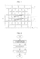
- FIG. 1 is a diagram illustrating the configuration of a printed board according to an embodiment of the present invention
- FIG. 1 is a diagram illustrating the configuration of a printed board according to the present embodiment.
- FIG. 2 is a diagram illustrating a method of manufacturing the printed board according to the present embodiment.
- a printed board 1 of the present embodiment includes an insulating body 11 that forms a flat surface; and printed wiring 12 that is laid out on the flat surface of the insulating body 11.
- glass cloth 111 is disposed inside the insulating body 11.
- the glass cloth 111 is insulating cloth woven from the vertical glass fibers (first fibers) and horizontal glass fibers (second fibers) that cross each other at right angles on the flat surface of the insulating body 11.
- the vertical fibers have a distance of 420 ⁇ m and the horizontal fibers have a distance of 440 ⁇ m according to the present embodiment.
- the printed wiring 12 also has a plurality of signal lines that includes the signal lines laid out parallel to each other at least. If a plurality of the signal lines includes the signal lines laid out in a different direction, the wiring direction of a plurality of the signal lines is assumed to be the direction of the longest signal line laid out among a plurality of the signal lines.
- the printed wiring 12 is laid out on the flat surface of the insulating body 11 in such a way that the wiring direction is tilted at 9 degrees to the direction of the glass fibers.
- FIG. 2 is a diagram illustrating a method of manufacturing the printed board according to the present embodiment.
- FIG. 3 is a diagram illustrating a film on which a wiring pattern is formed.
- a film 13 on which a wiring pattern 131 is formed as illustrated in FIG. 3 is attached to the insulating body 11 in such a way that the film 13 is tilted at 9 degrees to the glass fibers (S101).
- An exposure process is then performed for the insulating body 11 to which the film 13 is attached (S102).
- unnecessary conductors are removed by etching process and the wiring pattern 12 is formed on the insulating body 11 as a result (S103).
- the insulating body 11 is cut into pieces that fit the size of the commercial version of the printed board 1.
- FIG. 4 is a diagram illustrating a correlation between the board-cutting efficiency and the tilt angle of the printed wiring.
- the vertical axis represents the board-cutting efficiency
- the horizontal axis represents the tilt angle of the printed wiring.
- FIG. 5 is a diagram illustrating the tilt angle of the printed wiring and the delay-time difference.
- the board-cutting efficiency peaks at 0 degree and has the lowest value at 45 degrees, meaning that in the range of 0 to 45 degrees, the board-cutting efficiency increases as the tilt angle decreases.
- the delay-time difference between the signal lines comes to 17.5 ps (picosecond) at 9 degrees.
- the delay-time difference between signal lines be less than or equal to 20 ps.
- the tilt angle of the printed wiring 12 is 9 degrees, the smallest of all the tilt angles for which the delay-time difference is less than or equal to 20 ps.
- the printed wiring 12 whose tilt angle relative to the glass fibers is based on the board-cutting efficiency of the insulating body 11 and a predetermined delay-time difference between the signal lines. Therefore, it is possible to reduce the delay-time difference between the signal lines as well as to prevent impedance mismatching without decreasing the board-cutting efficiency.
Landscapes
- Engineering & Computer Science (AREA)
- Microelectronics & Electronic Packaging (AREA)
- Structure Of Printed Boards (AREA)
- Manufacturing Of Printed Wiring (AREA)
Abstract
A printed board includes an insulating body (11) that has a flat surface and includes insulating cloth (111) including first fibers and second fibers that cross the first fibers at right angles on the flat surface, and printed wiring (12) including a plurality of signal lines that run parallel to each other and are laid out on the flat surface of the insulating body so that a direction of the signal lines is tilted to a direction of the first or second fibers at an angle which is determined based on board-cutting efficiency of the insulating body (11) and a predetermined delay-time difference between the signal lines.
Description
- The technique disclosed herein relates to a printed board and a method of manufacturing the printed board.
- The frequency for high-speed transmission on a printed board is about to reach a range of 3 to 5 GHz. Differences in the delay time of signals therefore occur between signal lines on a printed board where a plurality of signal lines are laid out on an insulating body in which insulating cloth is disposed. The following describes the differences of delay time.
FIG. 6 is a diagram illustrating a printed board made of an insulating material where glass cloth is disposed.FIG. 7 is a diagram illustrating concave and convex portions of glass cloth and signal lines. As illustrated inFIG. 6 , a printed board 7 includes aninsulating body 71 that isglass cloth 711, which serves as insulating cloth, impregnated with resin; and printedwiring 72 including a plurality of signal lines that run parallel to each other. Theglass cloth 711 is woven from glass fibers that cross each other at right angles. As illustrated inFIG. 7 , on the printed board 7, a plurality of signal lines in the printedwiring 72 are located differently relative to the concave and convex portions of the glass fibers depending on where the signal lines are disposed. Much of the printedwiring 72 is parallel or at right angles to the glass fibers, in which case the position of each signal line in the printedwiring 72 relative to the concave and convex portions of the glass fibers is always constant. Since there is a difference in permittivity between the glass fibers and the resin, the distance from the glass fibers causes the differences in the delay time of signals between the signal lines. - A technique of laying out signal lines in a zigzag pattern is known to dissolve the differences of delay time.
FIG. 8 is a diagram illustrating signal lines laid out in a zigzag pattern. As illustrated inFIG. 8 , on a printedboard 8, printedwiring 82 is laid out in a zigzag pattern so as not to be parallel or at right angles to the glass fibers of theinsulating body 71. Thus, the distances between each of a plurality of signal lines in the printedwiring 82 and the glass fibers are never fixed. Therefore, it is possible to reduce the differences in the delay time of signals between the signal lines. However, the zigzag pattern makes the lines longer than the normal way of wiring, making it impossible to propagate high-speed signals in a stable manner in the range of 5 to 10 GHz. Moreover, the zigzag pattern leads to deterioration of signal waveforms, reductions in the density of wiring, increasing transmission loss and the like due to the longer lines. - A technique of providing the printed wiring tilted at 45 degrees to an insulating body is known to solve the above problem.
FIG. 9 is a diagram illustrating a printed board whose printed wiring is tilted at 45 degrees to an insulating body. As illustrated inFIG. 9 , on a printedboard 9, printedwiring 91 as a whole is tilted at 45 degrees to the insulatingbody 71 in order to obtain the same effect as the zigzag pattern does without changing the routes of a plurality ofsignal lines 911. Therefore, the differences of delay time between thesignal lines 911 decrease without leading to deterioration of signal waveforms, reductions in the density of wiring, increased transmission losses and the like. - Patent Document 1: Japanese Laid-open Patent Publication No.
2008-193073
Patent Document 2: Japanese Laid-open UM Publication No.05-15467 - However, as illustrated in
FIG. 9 , the 45-degree tilting of the printedwiring 91 on theinsulating body 71 requires a largerinsulating body 71 compared with the one that is not tilted, resulting in a significant decrease in the efficiency of cutting the board. - It is therefore desirable to develop a technique to solve the above problems. An object of the technique disclosed herein is to provide a printed board and a method of manufacturing the printed board that may reduce the delay-time difference between signal lines without decreasing the board-cutting efficiency.
- According to an aspect of the invention, a printed board includes: an insulating body that has a flat surface and includes insulating cloth including first fibers and second fibers that cross the first fibers at right angles on the flat surface; and printed wiring including a plurality of signal lines that run parallel to each other and are laid out on the flat surface of the insulating body so that a direction of the signal lines is tilted to a direction of the first or second fibers at an angle which is determined based on board-cutting efficiency of the insulating body and a predetermined delay-time difference between the signal lines.
- The present invention is defined in the attached independent claims. Further, preferred features may be found in the dependent claims appended thereto.
-
FIG. 1 is a diagram illustrating the configuration of a printed board according to an embodiment of the present invention; -
FIG. 2 is a diagram illustrating a method of manufacturing the printed board according to an embodiment of the present invention; -
FIG. 3 is a diagram illustrating a film on which a wiring pattern is formed; -
FIG. 4 is a diagram illustrating a correlation between board-cutting efficiency and tilt angle of printed wiring; -
FIG. 5 is a diagram illustrating the tilt angle of the printed wiring and delay-time difference; -
FIG. 6 is a diagram illustrating a printed board made of an insulating material where glass cloth is disposed; -
FIG. 7 is a diagram illustrating concave and convex portions of glass cloth and signal lines; -
FIG. 8 is a diagram illustrating signal lines laid out in a zigzag pattern; and -
FIG. 9 is a diagram illustrating a printed board whose printed wiring is tilted at 45 degrees to an insulating body. - Hereinafter, an embodiment of the present invention will be described with reference to the accompanying drawings.
- Described first is a printed board of the present embodiment.
FIG. 1 is a diagram illustrating the configuration of a printed board according to the present embodiment.FIG. 2 is a diagram illustrating a method of manufacturing the printed board according to the present embodiment. - As illustrated in
FIG. 1 , a printedboard 1 of the present embodiment includes aninsulating body 11 that forms a flat surface; and printedwiring 12 that is laid out on the flat surface of theinsulating body 11. Inside the insulatingbody 11,glass cloth 111 is disposed. Theglass cloth 111 is insulating cloth woven from the vertical glass fibers (first fibers) and horizontal glass fibers (second fibers) that cross each other at right angles on the flat surface of theinsulating body 11. As for the distance between the glass fibers running in the same direction on theglass cloth 111, the vertical fibers have a distance of 420µm and the horizontal fibers have a distance of 440µm according to the present embodiment. The printedwiring 12 also has a plurality of signal lines that includes the signal lines laid out parallel to each other at least. If a plurality of the signal lines includes the signal lines laid out in a different direction, the wiring direction of a plurality of the signal lines is assumed to be the direction of the longest signal line laid out among a plurality of the signal lines. The printedwiring 12 is laid out on the flat surface of theinsulating body 11 in such a way that the wiring direction is tilted at 9 degrees to the direction of the glass fibers. - The following describes a method of manufacturing a printed board according to the present embodiment.
FIG. 2 is a diagram illustrating a method of manufacturing the printed board according to the present embodiment.FIG. 3 is a diagram illustrating a film on which a wiring pattern is formed. - As illustrated in
FIG. 2 , in a process of manufacturing the printedboard 1, afilm 13 on which awiring pattern 131 is formed as illustrated inFIG. 3 is attached to theinsulating body 11 in such a way that thefilm 13 is tilted at 9 degrees to the glass fibers (S101). An exposure process is then performed for theinsulating body 11 to which thefilm 13 is attached (S102). After the exposure process, unnecessary conductors are removed by etching process and thewiring pattern 12 is formed on theinsulating body 11 as a result (S103). After the formation of thewiring pattern 12, theinsulating body 11 is cut into pieces that fit the size of the commercial version of the printedboard 1. - The following describes a correlation between the board-cutting efficiency and the tilt angle of the printed wiring as well as the tilt angle and the delay-time difference.
FIG. 4 is a diagram illustrating a correlation between the board-cutting efficiency and the tilt angle of the printed wiring. InFIG. 4 , the vertical axis represents the board-cutting efficiency, while the horizontal axis represents the tilt angle of the printed wiring.FIG. 5 is a diagram illustrating the tilt angle of the printed wiring and the delay-time difference. - As illustrated in
FIG. 4 , the board-cutting efficiency peaks at 0 degree and has the lowest value at 45 degrees, meaning that in the range of 0 to 45 degrees, the board-cutting efficiency increases as the tilt angle decreases. As illustrated inFIG. 5 , when the delay-time difference between the signal lines is measured at each tilt angle, the delay-time difference comes to 17.5 ps (picosecond) at 9 degrees. In general, it is preferable that the delay-time difference between signal lines be less than or equal to 20 ps. According to the present embodiment, the tilt angle of the printedwiring 12 is 9 degrees, the smallest of all the tilt angles for which the delay-time difference is less than or equal to 20 ps. That is, according to the present embodiment, what is formed on the insulatingbody 11 of the printedboard 1 is the printedwiring 12 whose tilt angle relative to the glass fibers is based on the board-cutting efficiency of the insulatingbody 11 and a predetermined delay-time difference between the signal lines. Therefore, it is possible to reduce the delay-time difference between the signal lines as well as to prevent impedance mismatching without decreasing the board-cutting efficiency. - It is possible to reduce the delay-time difference between signal lines without decreasing the board-cutting efficiency.
Claims (6)
- A printed board comprising:an insulating body that has a flat surface and includes insulating cloth including first fibers and second fibers that cross the first fibers at right angles on the flat surface; andprinted wiring including a plurality of signal lines that run parallel to each other and are laid out on the flat surface of the insulating body so that a direction of the signal lines is tilted to a direction of the first or second fibers at an angle which is determined based on board-cutting efficiency of the insulating body and a predetermined delay-time difference between the signal lines.
- The printed board according to claim 1, wherein the angle is 9 degrees.
- The printed board according to claim 1 or 2, wherein the predetermined delay-time difference is 20 picoseconds.
- A method of manufacturing a printed board, the method comprising:forming a flat surface on an insulating body including insulating cloth which includes first fibers and second fibers, so that the second fibers cross the first fibers at right angles on the flat surface; anddisposing printed wiring including a plurality of signal lines that run parallel to each other so that a direction of the signal lines on the flat surface is tilted to a direction of the first or second fibers at an angle which is determined based on board-cutting efficiency of the insulating body and a predetermined delay-time difference between the signal lines.
- The method of manufacturing the printed board according to claim 4, wherein the angle is 9 degrees.
- The method of manufacturing the printed board according to claim 4 or 5, wherein the predetermined delay-time difference is 20 picoseconds.
Applications Claiming Priority (1)
| Application Number | Priority Date | Filing Date | Title |
|---|---|---|---|
| JP2009226189A JP5299201B2 (en) | 2009-09-30 | 2009-09-30 | Printed circuit board and printed circuit board manufacturing method |
Publications (1)
| Publication Number | Publication Date |
|---|---|
| EP2306793A1 true EP2306793A1 (en) | 2011-04-06 |
Family
ID=42797132
Family Applications (1)
| Application Number | Title | Priority Date | Filing Date |
|---|---|---|---|
| EP10174430A Withdrawn EP2306793A1 (en) | 2009-09-30 | 2010-08-27 | Printed wiring board and method of manufacturing printed wiring board |
Country Status (5)
| Country | Link |
|---|---|
| US (1) | US8513537B2 (en) |
| EP (1) | EP2306793A1 (en) |
| JP (1) | JP5299201B2 (en) |
| CN (1) | CN102036468B (en) |
| TW (1) | TWI413465B (en) |
Families Citing this family (4)
| Publication number | Priority date | Publication date | Assignee | Title |
|---|---|---|---|---|
| JP2018082085A (en) * | 2016-11-17 | 2018-05-24 | イビデン株式会社 | Printed Wiring Board |
| CN108254625A (en) * | 2017-12-29 | 2018-07-06 | 生益电子股份有限公司 | A kind of insertion loss test-strips |
| JP2019158542A (en) * | 2018-03-13 | 2019-09-19 | 古河電気工業株式会社 | Radar device |
| JP2024066064A (en) * | 2022-11-01 | 2024-05-15 | ヒロセ電機株式会社 | Intermediate circuit board and intermediate electrical connector |
Citations (7)
| Publication number | Priority date | Publication date | Assignee | Title |
|---|---|---|---|---|
| JPH0515467U (en) | 1991-08-05 | 1993-02-26 | 住友電気工業株式会社 | Semiconductor element mounting structure |
| JP2004152874A (en) * | 2002-10-29 | 2004-05-27 | Sumitomo Electric Ind Ltd | Printed wiring board and method of cutting fiber reinforced synthetic resin material |
| US20060120059A1 (en) * | 2004-12-03 | 2006-06-08 | Dell Products L.P. | System and method for optimizing printed circuit boards to minimize effects of non-uniform dielectric |
| US20070110388A1 (en) * | 2005-11-17 | 2007-05-17 | Intel Corporation | Method of making a fiber reinforced printed circuit board panel and a fiber reinforced panel made according to the method |
| US20070178289A1 (en) * | 2006-01-27 | 2007-08-02 | International Business Machines Corporation | High-speed routing composite material |
| US20070182436A1 (en) * | 2006-02-07 | 2007-08-09 | Sun Microsystems, Inc. | Technique for offsetting signal lines from the glass weave of resin/glass materials |
| JP2008193073A (en) | 2007-02-07 | 2008-08-21 | Hon Hai Precision Industry Co Ltd | Printed circuit board and method for designing the printed circuit board |
Family Cites Families (11)
| Publication number | Priority date | Publication date | Assignee | Title |
|---|---|---|---|---|
| JP3187458B2 (en) | 1991-07-10 | 2001-07-11 | 株式会社資生堂 | Antimicrobial wet wipes, clean cotton, soft cloth towel |
| US5587890A (en) * | 1994-08-08 | 1996-12-24 | Cooper Industries, Inc. | Vehicle electric power distribution system |
| JPH10117048A (en) * | 1996-10-09 | 1998-05-06 | Tec Corp | Printed circuit board |
| US6657130B2 (en) * | 2001-09-20 | 2003-12-02 | International Business Machines Corporation | Electrical and physical design integration method and apparatus for providing interconnections on first level ceramic chip carrier packages |
| US6835889B2 (en) * | 2001-09-21 | 2004-12-28 | Kabushiki Kaisha Toshiba | Passive element component and substrate with built-in passive element |
| JP2006100699A (en) * | 2004-09-30 | 2006-04-13 | Toshiba Corp | Printed wiring board, information processing apparatus, and printed wiring board manufacturing method |
| EP1926357A3 (en) * | 2006-11-21 | 2009-09-30 | Ricoh Company, Ltd. | Functional device fabrication apparatus and functional device fabricated with the same |
| JP2008153386A (en) * | 2006-12-15 | 2008-07-03 | Toshiba Corp | Digital signal transmission board and computer |
| JP4915519B2 (en) * | 2007-03-16 | 2012-04-11 | 富士通株式会社 | Multilayer wiring board structure |
| JP2009073946A (en) * | 2007-09-21 | 2009-04-09 | Hitachi Ltd | Insulating substrate, wiring board and multilayer board |
| JP4538069B2 (en) * | 2008-11-28 | 2010-09-08 | 株式会社東芝 | Printed wiring board |
-
2009
- 2009-09-30 JP JP2009226189A patent/JP5299201B2/en not_active Expired - Fee Related
-
2010
- 2010-08-20 US US12/859,829 patent/US8513537B2/en not_active Expired - Fee Related
- 2010-08-20 TW TW099127967A patent/TWI413465B/en not_active IP Right Cessation
- 2010-08-27 EP EP10174430A patent/EP2306793A1/en not_active Withdrawn
- 2010-09-27 CN CN2010102979916A patent/CN102036468B/en not_active Expired - Fee Related
Patent Citations (7)
| Publication number | Priority date | Publication date | Assignee | Title |
|---|---|---|---|---|
| JPH0515467U (en) | 1991-08-05 | 1993-02-26 | 住友電気工業株式会社 | Semiconductor element mounting structure |
| JP2004152874A (en) * | 2002-10-29 | 2004-05-27 | Sumitomo Electric Ind Ltd | Printed wiring board and method of cutting fiber reinforced synthetic resin material |
| US20060120059A1 (en) * | 2004-12-03 | 2006-06-08 | Dell Products L.P. | System and method for optimizing printed circuit boards to minimize effects of non-uniform dielectric |
| US20070110388A1 (en) * | 2005-11-17 | 2007-05-17 | Intel Corporation | Method of making a fiber reinforced printed circuit board panel and a fiber reinforced panel made according to the method |
| US20070178289A1 (en) * | 2006-01-27 | 2007-08-02 | International Business Machines Corporation | High-speed routing composite material |
| US20070182436A1 (en) * | 2006-02-07 | 2007-08-09 | Sun Microsystems, Inc. | Technique for offsetting signal lines from the glass weave of resin/glass materials |
| JP2008193073A (en) | 2007-02-07 | 2008-08-21 | Hon Hai Precision Industry Co Ltd | Printed circuit board and method for designing the printed circuit board |
Also Published As
| Publication number | Publication date |
|---|---|
| CN102036468A (en) | 2011-04-27 |
| US8513537B2 (en) | 2013-08-20 |
| CN102036468B (en) | 2013-05-01 |
| JP2011077237A (en) | 2011-04-14 |
| JP5299201B2 (en) | 2013-09-25 |
| US20110073354A1 (en) | 2011-03-31 |
| TWI413465B (en) | 2013-10-21 |
| TW201112898A (en) | 2011-04-01 |
Similar Documents
| Publication | Publication Date | Title |
|---|---|---|
| CN102479990B (en) | Microstrip line structure | |
| US7515015B2 (en) | High speed signal transmission structure | |
| WO2012140422A1 (en) | A substrate integrated waveguide to air filled waveguide transition | |
| US7043706B2 (en) | Conductor trace design to reduce common mode cross-talk and timing skew | |
| EP2306793A1 (en) | Printed wiring board and method of manufacturing printed wiring board | |
| JP2022520700A (en) | Antenna array based on one or more metamaterial structures | |
| US20160049714A1 (en) | Transition Between a SIW and a Waveguide Interface | |
| EP1654915B1 (en) | Circuit board design | |
| US20140326495A1 (en) | High performance printed circuit board | |
| US8058560B2 (en) | Bendable area design for flexible printed circuitboard | |
| EP1720213B1 (en) | Transducer circuit | |
| KR20100030568A (en) | Electromagnetic band gap tuning using undulating branches | |
| US20080186687A1 (en) | Printed circuit board | |
| US20090188699A1 (en) | Printed circuit board | |
| CN101356863B (en) | Method of making a fiber reinforced printed circuit board panel and a fiber reinforced panel made according to the method | |
| US20060108680A1 (en) | Multi-layer printed circuit board wiring layout and method for manufacturing the same | |
| US20080296049A1 (en) | Printed Circuit Board | |
| KR100992865B1 (en) | Transmissive Electromagnetic Refractor | |
| EP2555236A1 (en) | High-frequency circuit board | |
| KR20140102462A (en) | Electromagnetic bandgap structure and method for manufacturing the electromagnetic bandgap structure | |
| US10490873B2 (en) | Transmission line including first and second signal conductor patterns separated by a third non-signal conductor pattern with specified dimensional relationships there between | |
| KR20210032113A (en) | Transition structure between microstrip and hollow substrate integrated waveguide | |
| KR101085867B1 (en) | Waveguide Serial Coupled Polarization Converter and Its Design Method | |
| JP2009124259A (en) | Antenna device | |
| Sepaintner et al. | Cost-effective implementation of air-filled waveguides on printed circuit boards |
Legal Events
| Date | Code | Title | Description |
|---|---|---|---|
| PUAI | Public reference made under article 153(3) epc to a published international application that has entered the european phase |
Free format text: ORIGINAL CODE: 0009012 |
|
| AK | Designated contracting states |
Kind code of ref document: A1 Designated state(s): AL AT BE BG CH CY CZ DE DK EE ES FI FR GB GR HR HU IE IS IT LI LT LU LV MC MK MT NL NO PL PT RO SE SI SK SM TR |
|
| AX | Request for extension of the european patent |
Extension state: BA ME RS |
|
| 17P | Request for examination filed |
Effective date: 20111004 |
|
| 17Q | First examination report despatched |
Effective date: 20130708 |
|
| STAA | Information on the status of an ep patent application or granted ep patent |
Free format text: STATUS: THE APPLICATION IS DEEMED TO BE WITHDRAWN |
|
| 18D | Application deemed to be withdrawn |
Effective date: 20131119 |