US6657130B2 - Electrical and physical design integration method and apparatus for providing interconnections on first level ceramic chip carrier packages - Google Patents
Electrical and physical design integration method and apparatus for providing interconnections on first level ceramic chip carrier packages Download PDFInfo
- Publication number
- US6657130B2 US6657130B2 US09/956,679 US95667901A US6657130B2 US 6657130 B2 US6657130 B2 US 6657130B2 US 95667901 A US95667901 A US 95667901A US 6657130 B2 US6657130 B2 US 6657130B2
- Authority
- US
- United States
- Prior art keywords
- ground
- line
- lines
- power
- signal
- Prior art date
- Legal status (The legal status is an assumption and is not a legal conclusion. Google has not performed a legal analysis and makes no representation as to the accuracy of the status listed.)
- Expired - Fee Related
Links
Images


Classifications
-
- H—ELECTRICITY
- H01—ELECTRIC ELEMENTS
- H01L—SEMICONDUCTOR DEVICES NOT COVERED BY CLASS H10
- H01L23/00—Details of semiconductor or other solid state devices
- H01L23/48—Arrangements for conducting electric current to or from the solid state body in operation, e.g. leads, terminal arrangements ; Selection of materials therefor
- H01L23/488—Arrangements for conducting electric current to or from the solid state body in operation, e.g. leads, terminal arrangements ; Selection of materials therefor consisting of soldered or bonded constructions
- H01L23/498—Leads, i.e. metallisations or lead-frames on insulating substrates, e.g. chip carriers
- H01L23/49822—Multilayer substrates
-
- H—ELECTRICITY
- H01—ELECTRIC ELEMENTS
- H01L—SEMICONDUCTOR DEVICES NOT COVERED BY CLASS H10
- H01L23/00—Details of semiconductor or other solid state devices
- H01L23/48—Arrangements for conducting electric current to or from the solid state body in operation, e.g. leads, terminal arrangements ; Selection of materials therefor
- H01L23/488—Arrangements for conducting electric current to or from the solid state body in operation, e.g. leads, terminal arrangements ; Selection of materials therefor consisting of soldered or bonded constructions
- H01L23/498—Leads, i.e. metallisations or lead-frames on insulating substrates, e.g. chip carriers
- H01L23/49838—Geometry or layout
-
- H—ELECTRICITY
- H01—ELECTRIC ELEMENTS
- H01L—SEMICONDUCTOR DEVICES NOT COVERED BY CLASS H10
- H01L23/00—Details of semiconductor or other solid state devices
- H01L23/48—Arrangements for conducting electric current to or from the solid state body in operation, e.g. leads, terminal arrangements ; Selection of materials therefor
- H01L23/50—Arrangements for conducting electric current to or from the solid state body in operation, e.g. leads, terminal arrangements ; Selection of materials therefor for integrated circuit devices, e.g. power bus, number of leads
-
- H—ELECTRICITY
- H01—ELECTRIC ELEMENTS
- H01L—SEMICONDUCTOR DEVICES NOT COVERED BY CLASS H10
- H01L2924/00—Indexing scheme for arrangements or methods for connecting or disconnecting semiconductor or solid-state bodies as covered by H01L24/00
- H01L2924/0001—Technical content checked by a classifier
- H01L2924/0002—Not covered by any one of groups H01L24/00, H01L24/00 and H01L2224/00
-
- H—ELECTRICITY
- H01—ELECTRIC ELEMENTS
- H01L—SEMICONDUCTOR DEVICES NOT COVERED BY CLASS H10
- H01L2924/00—Indexing scheme for arrangements or methods for connecting or disconnecting semiconductor or solid-state bodies as covered by H01L24/00
- H01L2924/15—Details of package parts other than the semiconductor or other solid state devices to be connected
- H01L2924/151—Die mounting substrate
- H01L2924/1517—Multilayer substrate
- H01L2924/15172—Fan-out arrangement of the internal vias
- H01L2924/15173—Fan-out arrangement of the internal vias in a single layer of the multilayer substrate
-
- H—ELECTRICITY
- H01—ELECTRIC ELEMENTS
- H01L—SEMICONDUCTOR DEVICES NOT COVERED BY CLASS H10
- H01L2924/00—Indexing scheme for arrangements or methods for connecting or disconnecting semiconductor or solid-state bodies as covered by H01L24/00
- H01L2924/30—Technical effects
- H01L2924/301—Electrical effects
- H01L2924/3011—Impedance
-
- Y—GENERAL TAGGING OF NEW TECHNOLOGICAL DEVELOPMENTS; GENERAL TAGGING OF CROSS-SECTIONAL TECHNOLOGIES SPANNING OVER SEVERAL SECTIONS OF THE IPC; TECHNICAL SUBJECTS COVERED BY FORMER USPC CROSS-REFERENCE ART COLLECTIONS [XRACs] AND DIGESTS
- Y10—TECHNICAL SUBJECTS COVERED BY FORMER USPC
- Y10T—TECHNICAL SUBJECTS COVERED BY FORMER US CLASSIFICATION
- Y10T29/00—Metal working
- Y10T29/49—Method of mechanical manufacture
- Y10T29/49002—Electrical device making
- Y10T29/49117—Conductor or circuit manufacturing
- Y10T29/49124—On flat or curved insulated base, e.g., printed circuit, etc.
- Y10T29/4913—Assembling to base an electrical component, e.g., capacitor, etc.
-
- Y—GENERAL TAGGING OF NEW TECHNOLOGICAL DEVELOPMENTS; GENERAL TAGGING OF CROSS-SECTIONAL TECHNOLOGIES SPANNING OVER SEVERAL SECTIONS OF THE IPC; TECHNICAL SUBJECTS COVERED BY FORMER USPC CROSS-REFERENCE ART COLLECTIONS [XRACs] AND DIGESTS
- Y10—TECHNICAL SUBJECTS COVERED BY FORMER USPC
- Y10T—TECHNICAL SUBJECTS COVERED BY FORMER US CLASSIFICATION
- Y10T29/00—Metal working
- Y10T29/49—Method of mechanical manufacture
- Y10T29/49002—Electrical device making
- Y10T29/49117—Conductor or circuit manufacturing
- Y10T29/49124—On flat or curved insulated base, e.g., printed circuit, etc.
- Y10T29/49155—Manufacturing circuit on or in base
- Y10T29/49158—Manufacturing circuit on or in base with molding of insulated base
- Y10T29/4916—Simultaneous circuit manufacturing
Definitions
- This invention relates to the field of integrated circuit chip packaging, and more specifically to packaging semiconductor chips on a substrate comprised of multilayer thin and/or thick (e.g. multilayer ceramic or organic) films.
- U.S. Pat. No. 4,866,507 of Jacobs et al. for “Module for Packaging Semiconductor Integrated Circuit Chips on a Base Substrate” describes a structure with alternating insulating and conductive layers formed on a substrate. Some of the conductive layers are patterned to have substantially coplanar spaced apart power/ground lines and signal lines on each layer with interconnections between power/ground lines on different levels forming a power/ground plane at the appropriate voltage level in three dimensions.
- a semiconductor carrier and a corresponding method for forming the carrier are provided for interconnecting ground, signal and power lines in a semiconductor carrier.
- the method of forming the carrier of this invention involves forming a stack of a plurality of insulating layers with generally parallel conductor lines including power lines and ground lines formed in planes therebetween with the generally parallel lines directed in orthogonal directions between any two of the insulating layers with alternation between planes of X-directed lines and planes of Y-directed lines and power lines and ground (reference potential) lines (networks) formed in parallel in a single plane.
- Form Z-directed via connections between planes connecting a power line in one plane to another power line in another plane.
- the signal line and the continuing line segment are connected by one or more Z-directed vias passing through at least one insulating layer.
- the signal line and the continuing line segment are connected by a via passing through at least one insulating layer and preferred that the signal line is between a power line and a ground line and the continuing line segment is between another power line and another ground line.
- a coplanar group of ground, power and signal lines are formed in parallel in a single plane in a surface of one of the insulating layers.
- the signal line and the continuing line segment are connected by a via passing through at least one insulating layer.
- the signal line is between a power line and a ground line and the continuing line segment is between another power line and another ground line.
- a coplanar group of ground, power and signal lines are formed in parallel in a single plane in a surface of one of the insulating layers between a layer of top surface metallurgy (TSM) on top and a layer of bottom surface metallurgy (BSM) on the bottom.
- TSM top surface metallurgy
- BSM bottom surface metallurgy
- vias directed along the vertical Z axis interconnecting respective power, ground and signal lines.
- the concept of this invention is independent of whether thin or thick multilayers are used, but its actual thick film ceramic hardware embodiment is important for proving the robustness and ease of applicability of the concept, not to overlook the importance of proving the feasibility of applying the idea.
- FIGS. 1A-1C show prior art mesh planes in a standard embodiment of a multilayer ceramic chip carrier package.
- FIG. 1A is a sectional plan view of the prior art multilayer ceramic stack which contains mesh patterned conductive planes and vias looking along the Z axis in a section taken along line 1 A- 1 A′ in FIGS. 1B and 1C.
- FIG. 1B is a sectional view taken along line 1 B- 1 B′ in FIG. 1 A.
- FIG. 1C is a sectional view taken along line 1 C- 1 C′ in FIG. 1 A.
- FIGS. 2A-2C are views of an embodiment of the present invention.
- FIG. 2A is a sectional plan view of a multilayer ceramic stack which contains mesh patterned conductive planes and vias looking along the Z axis in a section taken along line 2 A- 2 A′ in FIGS. 2B and 2C.
- FIG. 2B is a sectional view taken along line 2 B- 2 B′ in FIG. 2 A.
- FIG. 2C is a sectional view taken along line 2 C- 2 C′ in FIG. 2 A.
- FIG. 3A shows modifications to the sectional view of the stack of FIG. 2A showing signal lines in the PVD carrier of this invention.
- FIG. 3B is a sectional plan view of the stack 30 of FIG. 3A taken along line 3 B- 3 B′ in FIG. 2 B.
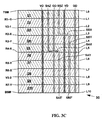
- FIG. 3C shows an elevational view of various illustrative via connections and interconnections of signal lines through a thicker more typical embodiment of the carrier of this invention.
- FIG. 4 illustrates how in accordance with the prior art STD method, a typical multilayer layer sequence starts with a dedicated Full Dense Square Hatch (FDSH) ground mesh plane GMP.
- FDSH Full Dense Square Hatch
- FIG. 5 shows a prior art dedicated Signal Redistribution Plane (SRP).
- SRP Signal Redistribution Plane
- FIG. 6 shows the next layer which is a prior art STD dedicated Full Dense Square Hatch (FDSH) Power Mesh Plane (PMP).
- FDSH Full Dense Square Hatch
- PMP Power Mesh Plane
- FIG. 7 shows the Top Surface Metallurgy (TSM) layer which is formed on the top of the top ceramic layer of FIG. 3C, although it is not shown in FIG. 3 C.
- TSM Top Surface Metallurgy
- FIG. 8 shows the R- 1 Y layer also referred to as the Bottom of Top Surface Metallurgy (BTSM) formed on the bottom of this first ceramic dielectric layer.
- BTSM Bottom of Top Surface Metallurgy
- FIG. 9 shows the V 2 - 1 layer formed on the bottom of the second ceramic, dielectric layer which interconnects many of the chip C 4 voltage vias dropping from the TSM layer of FIG. 7 .
- FIG. 10 shows the R 2 -X layer formed on the bottom of the third dielectric layer.
- FIG. 11 shows R 3 -Y layer formed on the bottom of the fourth dielectric layer.
- FIG. 12 shows R 4 -X layer formed on the bottom of the fifth dielectric layer.
- FIG. 13 shows R 5 -Y layer formed on the bottom of the sixth dielectric layer.
- FIG. 14 shows R 6 -X layer formed on the bottom of the seventh dielectric layer.
- FIG. 15 shows V 2 - 2 layer formed on the bottom of the eighth dielectric layer.
- FIG. 16 shows R 7 -Y layer formed on the bottom of the ninth dielectric layer.
- FIG. 17 shows BSM layer L 10 formed on the bottom of the tenth dielectric layer.
- the integrated circuit chip packaging structure of this invention provides high density physical design for signal C 4 (Controlled Collapse Chip Connection, i.e. solder ball) to I/O (Input/Output) wiring, with excellent electrical characteristics and performance, such as low impedance power distribution, ZO impedance matching, relatively low signal line coupled noise, acceptable signal line resistance, excellent signal line shielding and current return paths provided by power and ground bus lines, uniform metal loading per layer, low camber or flatness of thick films, low via bulge, relatively fewer layers, smaller impact on ground rules, manufacturing processes and materials, and ease of physical design technique.
- relative means comparison with the STandard Design (STD) method, which results in the usual packaging structures with dedicated explicit power and ground mesh or solid metal structures, each formed in a single plane, to separate the dedicated signal line redistribution layers.
- STD STandard Design
- this invention uses a coplanar arrangement of power, ground and signal lines on each layer, with no interspersed dedicated, explicit power and ground layers.
- the method of this invention is referred to as the Perfect Vertical Design (PVD), hereinbelow.
- Jacobs et al. U.S. Pat. No. 4,866,507 (cited above) illustrates the problem solved by the present invention.
- the principal differences between the Jacobs et al. patent and the present invention are that Jacobs et al. addressed the features as follows:
- the present invention can successfully provide the advantageous features as follows:
- ball e.g. C 4 solder ball
- column grid area arrays for connection to a second level package
- PVD Perfect Vertical Design
- STD STandard Design
- FIG. 1A is a sectional plan view of a prior art multilayer ceramic stack 10 which contains mesh patterned conductive planes and vias looking along the Z axis in a section taken along line 1 A- 1 A′ in FIGS. 1B and C which as can be seen in FIGS. 1B and 1C shows a power plane mesh layer 18 at the bottom of a ceramic layer 21 .
- FIG. 1B is a sectional view taken along line 1 B- 1 B′ in FIG. 1 A.
- FIG. 1C is a sectional view taken along line 1 C- 1 C′ in FIG. 1 A.
- the prior art stack 10 is formed of a plurality of parallel ceramic layers 13 , 15 , 17 , 19 , and 21 which extend horizontally parallel to the X and Y axes in FIG. 1 A.
- the ceramic layers 13 , 15 , 17 , 19 , and 21 are stacked one upon the other from the bottom to the top of stack 10 , including ceramic layer 13 on the bottom, ceramic layer 15 , ceramic layer 17 , ceramic layer 19 and ceramic layer 21 on the top.
- the ceramic layers 13 , 15 , 19 , and 21 include mesh-patterned, conductive planes 12 , 14 , 16 and 18 for providing electrical ground or electrical power connections and signal net segment SG 1 formed in part on the bottom of layer 17 , as explained in more detail below.
- FIG. 1A shows top views of nine parallel, vertical conductors including four power vias PV 1 , PV 2 , PV 3 , PV 4 , three ground vias GV 1 , GV 2 , GV 3 , and two signal vias SV 1 and SV 2 (with signal via SV 2 being shown in phantom in that view).
- Each of the signal vias SV 1 and SV 2 pass through some of the ceramic layers to provide interconnections to the opposite ends of the signal net segment SG 1 , which is shown in phantom in FIG. 1 A and in section in FIG. 1B, as are the signal vias SV 1 and SV 2 .
- the other seven vias pass through all of the ceramic layers to provide seven electrical interconnections between the ground planes 12 and 16 or the power planes 14 and 18 respectively.
- Each of the mesh-patterned, conductive ground planes 12 and 16 and the power planes 14 and 18 has conductive portions which extend orthogonally, i.e. in both the X and Y directions in the single layer at the bottom of the respective one of the ceramic dielectric layers 13 , 15 , 19 and 21 .
- connection links CL to the power vias PV 1 , PV 2 , PV 3 , PV 4 which are centered in the squares formed by the X and Y stripes of the mesh.
- Similar connection links CL′ are shown in phantom connecting ground planes 12 and 16 to ground vias GV 1 , GV 2 and GV 3 .
- FIG. 1B is a sectional view of the stack 10 taken along line 1 B- 1 B′ in FIG. 1A which shows the stack of several dielectric layers 13 , 15 , 17 , 19 and 21 that contain various conductive mesh planes or a signal conductor formed in the lower surfaces thereof and showing the vertically extending ground via GV 2 passing through all of the dielectric layers 13 , 15 , 17 , 19 and 21 .
- the combination of the signal via SV 1 and signal via SV 2 extend in parallel, vertically, from the top to the bottom, of the stack 10 with their connections to signal conductor SG 1 .
- FIG. 1C is a sectional view of the stack 10 taken along line 1 C- 1 C′ in FIG. 1A which shows the stack of several dielectric layers 13 , 15 , 17 , 19 and 21 that contain various conductors and showing vertically extending power vias PV 3 and PV 4 and ground via GV 3 extending in parallel, vertically, from the top to the bottom, of the stack 10 passing through all of the ceramic dielectric layers 13 , 15 , 17 , 19 and 21 .
- a first mesh-patterned, conductive, ground plane 12 is formed in the bottom surfaces of the bottom ceramic layer 13 .
- a second mesh-patterned, conductive, ground plane 16 is formed in the bottom surface of the ceramic layer 19 .
- a mesh-patterned, conductive, power plane 14 is formed in the bottom surface of the ceramic layer 15 .
- a second mesh-patterned, conductive power plane 18 is formed in the bottom surface of the top ceramic layer 21 .
- a linear conductive signal net segment SG 1 is formed in the bottom surface of the layer 17 .
- FIG. 1B shows the connections to the center left of FIG. 1A, which shows ground via GV 2 providing the interconnections between ground plane 12 and ground plane 16 on the left of FIG. 1 B.
- FIG. 1C shows the connection to the bottom center of FIG. 1A, which shows ground via GV 3 which also provide interconnections between ground plane 12 and ground plane 16 in the center of FIG. 1 C.
- the four power vias PV 1 , PV 2 , PV 3 and PV 4 connect the power plane 14 to power plane 18 .
- Two of the power vias PV 3 and PV 4 located in the lower left and lower right corners of FIG. 1A provide interconnections between power plane 14 and power plane 18 as seen in FIG. 1 C.
- the power vias PV 1 and PV 2 which are located near to the upper left and upper right corners of FIG. 1A pass through the ceramic layers to provide interconnections between the power plane 14 and the power plane 18 in like manner to vias PV 3 and PV 4 .
- the signal via SV 1 passes through top ceramic layer 21 , layer 19 and to the signal net segment SG 1 on the bottom of ceramic layer 17 which is directed along parallel to the X-axis to signal via SV 2 which passes down through the ceramic layers 15 and 13 to the bottom of the stack 10 for connection to termination points beyond the structure shown which is a fragment of a more complex structure that has been simplified for convenience of explanation and illustration of the prior art.
- the top level of the stack 10 includes upper power plane mesh 18 at the bottom of the top dielectric layer 21 and above the second dielectric layer 19 .
- the upper ground plane mesh 16 is formed in the bottom of the second dielectric layer 19 , as shown in FIGS. 1B and 1C.
- the lower power plane mesh 14 is formed in the bottom of the fourth dielectric layer 15 of the stack 10 .
- Formed in the bottom dielectric layer 13 of the stack 10 is the ground plane mesh 12 .
- Power plane mesh 18 comprises a conductive grid layer which extends orthogonally, i.e. in the X and Y directions in a single planar layer pressed into the bottom surface of the top dielectric layer 21 which is preferably formed of a ceramic material through which the various vias PV 1 -PV 4 , GV 1 -GV 3 and SV 1 extend.
- the orthogonal power mesh layer 18 is at the same electrical voltage level as the lower power mesh layer 14 because they are interconnected by the power vias PV 1 -PV 4 .
- FIGS. 2A-2C are views of an embodiment of the present invention.
- FIG. 2A is a sectional plan view of a multilayer ceramic stack 30 which contains coplanar patterned conductive planes and vias looking along the Z axis in a section taken along line 2 A- 2 A′ in FIGS. 2B and 2C.
- FIG. 2B is a sectional view taken along line 2 B- 2 B′ in FIG. 2 A.
- FIG. 2C is a sectional view taken along line 2 C- 2 C′ in FIG. 2 A.
- FIG. 2A from the bottom to the top of stack 30 there are four ceramic, dielectric layers 33 , 35 , 37 and 39 formed on a substrate, not shown for convenience of illustration.
- FIG. 2A there are four parallel conductor lines 38 A, 38 B, 38 C and 38 D in the base of the upper dielectric layer 39 , with those lines extending parallel to the Y axis including two power/voltage lines 38 A and 38 C alternating with two ground lines 38 B and 38 D.
- the power/voltage lines 36 B and 36 D are connected to power/voltage lines 38 A and 38 C by power vias 40 A, 40 C, 40 B and 40 D.
- the ground lines 36 A and 36 C are connected to ground lines 38 B and 38 D by ground vias 42 A and 42 C reaching up to ground line 38 B from ground lines 36 C and 36 A respectively and ground vias 42 D and 42 B reaching up to ground line 38 D from ground lines 36 A and 36 C respectively.
- the vias holes parallel to the Z axis are either drilled or punched, and then filled with a conductive material which forms the conductive vias in the final stack 30 .
- the original single standard mesh plane has been replaced by two coplanar metal layers with power/voltage lines 38 A/ 38 C and ground lines 38 B/ 38 D all Y-directed on the first layer and with power/voltage lines 36 B/ 36 D and ground mesh lines 36 A, 36 C all X-directed on the second layer, with the interposed dielectric material of layer 37 which prevents electrical short circuiting.
- Vertical power/voltage vias 40 A, 40 B, 40 C and 40 D and vertical ground vias 42 A, 42 B, 42 C and 42 D which are punched through this dielectric, electrically interconnect the two separate sets of orthogonal voltage and ground mesh or bus lines.
- the orthogonal set of voltage (or ground) bus lines of this PVD structure is essentially electrically equivalent to, but topologically different from the original standard mesh voltage (or ground) plane.
- the integrated mesh or bus line PVD carrier in accordance with this invention of FIGS. 2A-2C forms a complete power distribution system with the usual requirements of low impedance to D.C. and A.C. current flow.
- FIG. 2A is a plan view of a stack 30 which is a section taken along line 2 A- 2 A′ in FIGS. 2B and 2C of ceramic layers in which conductive circuit patterns are formed and through which vias extend.
- FIG. 2B is a sectional view of the stack 30 showing the stack of ceramic dielectric layers 33 , 35 , 37 and 39 that contain various conductors, as described below showing an array of ground vias 42 A, 42 B extending in parallel from the top to the bottom of stack 30 .
- the ground vias 42 A/ 42 B connect respectively to Y-directed ground stripes 38 B/ 38 D at the bottom of ceramic layer 39 .
- Both ground vias 42 A, 42 B connect to X-directed ground stripe 36 C at the bottom of lower ceramic layer 37 .
- the ground vias 42 A/ 42 B connect respectively to Y-directed ground stripes 34 B/ 34 D at the bottom of the ceramic layer 35 .
- both ground vias 42 A, 42 B connect to X-directed ground stripe 32 C at the bottom of the lowest ceramic layer 33 .
- the limited numbers of the layers 33 , 35 , 37 and 39 , the stripes therein and the vias therein, shown in the X, Y and Z directions are employed for convenience of illustration, as many more layers, stripes and vias are employed in a complete system embodiment, as will be well understood by those skilled in the art.
- FIG. 2C is a sectional view of stack 30 taken along line 1 C- 1 C′ in FIG. 1A showing the array of power vias 40 C and 40 D extending in parallel from the top to the bottom of the stack 30 .
- the power vias 40 C/ 40 D connect respectively to Y-directed power stripes 38 A/ 38 C at the bottom of the top ceramic layer 39 .
- Both power vias 40 C/ 40 D connect to X-directed power stripe 36 B at the bottom of lower ceramic layer 37 .
- Power vias 40 C/ 40 D connect respectively to Y-directed power stripes 34 A/ 34 C at the bottom of ceramic layer 35 .
- power vias 40 C, 40 D both connect to X-directed power stripe 32 B at the bottom of the lowest ceramic layer 33 .
- FIG. 3A shows a modification to the sectional plan view of stack 30 of FIG. 2 A.
- FIG. 3B is a sectional plan view of the stack 30 of FIG. 3A taken along line 3 B- 3 B′ in FIG. 2 B.
- FIGS. 3A and 3B show signal nets SG 1 /SG 1 ′ and SG 2 /SG 2 ′ in the PVD carrier of this invention.
- the lines comprising signal net segments SG 1 and SG 2 are Y-directed.
- Signal net segment SG 1 is routed between the voltage/power line 38 A and the ground bus line 38 B where it reaches signal via 52 which extends in the Z direction.
- Signal net segment SG 2 is routed between the voltage/power line 38 C and the ground bus line 38 B.where it reaches signal via 62 which extends in the Z direction.
- the lines comprising signal net segments SG 1 ′ and SG 2 ′ are X-directed.
- Signal nets segment SG 1 ′ is routed from the Z directed signal via 52 between the voltage/power line 36 B and the ground bus line 36 C.
- Signal net segment SG 2 ′ is routed from the Z directed signal via 62 between the voltage/power line 36 B and the ground bus line 36 A.
- the PVD carrier 30 of FIGS. 3A and 3B there can be signal lines from a given signal net on each layer of this two layer power distribution system, so that one can have an integrated orthogonal system of adjacent sets of signal lines per signal net on multiple layers, with vertical vias interconnecting the signal lines when they change direction and hence their layer.
- These signal nets have excellent current return paths due to the presence of power and ground bus lines directly on either side thereof.
- the bus lines also provide electrical shielding of the neighboring lateral signal nets.
- the signal nets are electrically decoupled vertically, since they are wired in orthogonal directions or possibly at forty-five degree (45°) directions on adjacent layers.
- This system of well-defined signal wiring channels allows good impedance control when proper physical constraints are placed on the physical chip package.
- FIG. 3C shows an elevational view of various illustrative via connections and interconnections of signal lines through a thicker, more typical, embodiment of the carrier of this invention, with more layers.
- FIG. 3C shows various illustrative Z-directed via connections through a thicker more typical embodiment of the carrier 30 which includes the TSM (Top Surface Metallurgy) layer L 0 , R 1 Y metallurgy layer L 1 , V 2 - 1 layer L 2 , R 2 -X layer L 3 , R 3 -Y layer L 4 , R 4 -X layer L 5 , R 5 -Y layer L 6 , R 6 -X layer L 7 , V 2 - 2 layer L 8 , R 7 -Y layer L 9 and Bottom Surface Metallurgy (BSM) layer L 10 .
- TSM Top Surface Metallurgy
- the V 2 - 1 and V 2 - 2 layers L 2 and L 8 are explicit power/voltage layers.
- the R 1 -Y layer L 1 , R 3 -Y layer L 4 , R 5 -Y layer L 6 and R 7 -Y layer L 9 are redistribution layers with conductor lines extending in the Y-direction.
- Dielectric (ceramic) layers D 1 , D 2 , D 3 , D 4 , D 5 , D 6 , D 7 , D 8 , D 9 , and D 10 are shown which contain the various conductive layers L 0 and L 1 -L 10 at the bottom of the dielectric layers D 1 -D 10 .
- the R 2 -X layer L 3 , R 4 -X layer L 5 , and R 6 -X layer L 7 are redistribution layers with conductor lines extending in the X-direction. Note that there are voltage via VDA, voltage via VDB (drawn in phantom since it is in another plane than the section of FIG. 3 C), ground via GDA (drawn in phantom since it is in another plane than the section of FIG. 3C) and ground via GDB of the type which are described above.
- a pair of signal nets SA and SB are shown which are composed of net segments SAZ/SAX/SAZ′/SAY/SAZ′′ and net segments SBZ/SBX/SBZ′/SBY/SBZ′′ respectively.
- Signal nets SA and SB illustrate how the signal vias connect from the top to the bottom and laterally in a multilayer ceramic carrier 30 .
- Signal via SA is composed of parallel, Z-directed vias SAZ, SAZ′ and SAZ connected by X-directed component SAX on R 4 -X layer L 5 , plus a horizontal, Y-directed component SAY on R 5 -Y layer L 5 .
- Signal via SB is composed of parallel, Z-directed vias SBZ, SBZ′ and SBZ′′ (drawn in phantom since it is also in different plane than the section of FIG. 3C) connected by X-directed component SBX on R 2 -X layer L 3 ; and a horizontal, Y-directed component SBY on R 3 -Y layer L 4 .
- FIG. 4 illustrates how in accordance with the prior art STD method, a typical multilayer layer sequence starts with a dedicated Full Dense Square Hatch (FDSH) ground mesh plane GMP.
- FDSH Full Dense Square Hatch
- FIG. 5 shows a prior art dedicated Signal Redistribution Plane (SRP). Note that two consecutive concentric rings of signal C 4 's are redistributed on this single dedicated signal layer.
- SRP Signal Redistribution Plane
- FIG. 6 shows the next layer which is a prior art STD dedicated Full Dense Square Hatch (FDSH) Power Mesh Plane (PMP).
- FDSH Full Dense Square Hatch
- PMP Power Mesh Plane
- the chip power and ground C 4 vias must be systematically eliminated as the design proceeds through the multilayered cross-section stack. This will be electrically unacceptable in the near future as switching speeds, signal coupled noise and power distribution noise increase, while voltage transition levels decrease.
- the dedicated ground mesh plane GMP of FIG. 4 and the power mesh plane PMP of FIG. 6 of the STD use a large quantity of metal in their outer regions, which do not carry useful ground and power currents to the chip, and also only electrically shield or provide useful current return paths for the relatively few sparse outlying signal lines of the signal redistribution layer.
- Such Full Dense Square Hatch (FDSH) mesh planes require about forty percent (40%) metal on the lower surface of each layer with usual mesh line thicknesses. Thinner metallic solid ground and power planes are electrically superior, but such a configuration of thin conductors causes significant physical design and manufacturing challenges.
- the PVD structure/method of this invention provides a more systematic and effective physical (mechanical) and electrical design for routing the same two concentric rings of signal C 4 's in two successive physical layers, and gives better electrical performance as dictated by requirements of the near future. Also, the PVD structure/method of this invention usually produces a module design with two or three fewer layers when decoupling capacitors are required for a chip package.
- the wrong way horizontal X-directed coplanar lines of FIG. 11, and the wrong way vertical Y-directed coplanar lines of FIG. 12, are necessary for the signal, power and ground lines to escape from the sides of the chip which are parallel to the right way direction of coplanar lines on each of these respective layers.
- the present invention provides a true three-dimensional structure for the ground and power distribution system, and the signal redistribution is electrically well integrated with this ground and power distribution system.
- the name Perfect Vertical Design (PVD) is given to this design method.
- PVD Perfect Vertical Design
- This invention provides a multilayer thin and/or thick film PVDesign carrier made by the method of this invention which has been applied successfully to a ten (10) layer ceramic substrate with six hundred forty-eight (648) signal IOs on the chip and eight (8) decoupling capacitors (decaps) on its Top Surface Metallurgy (TSM).
- TSM Top Surface Metallurgy
- SCM Single Chip Module
- FIG. 7 shows the Top Surface Metallurgy (TSM) layer L 0 formed on the top of the first ceramic layer D 1 of FIG. 3C (above L 1 ).
- the center array of chip C 4 's consist of signal C 4 's, five different voltage level C 4 's, ground reference C 4 's and some unused dummy C 4 's.
- Eight decoupling capacitors surround the chip and have C 4 's for the five voltage levels and ground reference for the decoupling capacitors (decaps). All the chip and decoupling capacitor (decap) C 4 's are connected to the bottom of this first layer by vertical vias punched through the layer.
- FIG. 8 is an illustration of R- 1 Y layer L 1 also referred to as the Bottom of Top Surface Metallurgy (BTSM), which is formed on the bottom of the first ceramic layer D 1 .
- the BTSM layer L 1 has a predominantly vertical Y-direction of coplanar signal, power and ground lines. The minority of horizontal X-directed “wrong-way” lines are required so that signal, power and ground C 4 's on the left and right sides of the chip can escape.
- Signal vias and lines are between grey ground reference vias and lines and black voltage VD 1 vias and lines.
- the center ground reference mesh of layer L 1 (FIG. 8) interconnects many of the chip C 4 ground reference vias dropping from the TSM layer L 0 (FIG. 7 ), and serves as a source for the ground reference bus lines of BTSM (R 1 -Y) layer L 1 , which interconnect the rest of the TSM chip C 4 ground reference vias dropping from the TSM layer L 0 .
- FIG. 9 shows the center voltage VD 1 mesh of V 2 - 1 layer L 2 (formed on the bottom of the second ceramic, dielectric layer D 2 ) interconnects many of the chip C 4 voltage VD 1 vias dropping from the TSM layer L 0 (FIG. 7 ).
- FIG. 10 shows R 2 -X layer L 3 which is formed on the bottom of the third dielectric layer D 3 .
- FIG. 11 shows R 3 -Y layer L 4 which is formed on the bottom of the fourth dielectric layer D 4 .
- Each signal line has a power VD 1 bus line on one side and ground GND bus line on the other side. It should be clear that this is a very efficient way of integrating the physical and electrical design of a chip package without requiring any new manufacturing processes, materials or stressing normal MLC ground rules. It has been shown by calculations and measurements that PVD very often will reduce physical layers, improve electrical performance, and simplify the manufacturing of first level chip packages, relative to other design methods such as STD.
- the orthogonal sets of power VD 1 and ground GND bus lines on adjacent layers are systematically interconnected by vertical vias, and the shorter these vias(i.e. the thinner the layers), the more closely these orthogonal sets of power and ground bus lines approximate explicit Full Dense Square Hatch (FDSH) power and ground mesh planes. Yet the signal redistribution can also be done on the same layer as these power or ground bus lines, which provide the power and ground distribution system and also shield and provide current return paths for the signal nets.
- FDSH Full Dense Square Hatch
- the decoupling capacitors are connected to the various power and ground bus lines and thus to the small central mesh planes on layers L 1 , L 2 and L 3 , in order to shorten the power and ground current distribution paths for the TSM chip C 4 's.
- the decoupling capacitor (decap) connections are transparent to the PVD method when the pattern and pitch of the decoupling capacitor (decap) C 4 's are similar to that of the chip C 4 's. This is another example of where a more robust design method has removed arbitrariness (of the decoupling capacitor (decap) C 4 configuration) from the design problem for specific and correct reasons.
- the STD requires two extra mesh plane layers to connect these decoupling capacitors (decaps).
- FIG. 9 the more conventional power distribution for the other voltage levels VD 2 , VD 3 , VD 4 and VD 5 , is shown by the five-way segmented FDSH mesh plane, where the small center mesh for VD 1 helps interconnect the chip VD 1 C 4 's to their center meshes and coplanar VD 1 bus lines on the integrated coplanar signal, power and ground layers.
- VD 2 , VD 3 , VD 4 , VD 5 voltage levels on layers L 2 and L 8 The VD 2 , VD 3 , VD 4 , and VD 5 chip C 4 's, their two FDSH mesh planes and corresponding BSM balls are interconnected by strategically placed vertical vias to enhance their power distribution.
- PVD can be used with the STandard Design(STD) method to produce a hybrid design, which includes mesh planes where necessary.
- layer L 3 has a predominant horizontal direction for the coplanar signal, VD 1 and GND lines.
- the small center ground mesh is the main source for the ground GND bus lines on this layer.
- FIG. 12 shows R 4 -X layer L 5 which is formed on the bottom of the fifth dielectric layer D 5 .
- FIG. 13 shows R 5 -Y layer L 6 which is formed on the bottom of the sixth dielectric layer D 6 .
- FIG. 14 shows R 6 -X layer L 7 which is formed on the bottom of the seventh dielectric layer D 7 .
- FIG. 15 shows V 2 - 2 layer L 8 which is formed on the bottom of the eighth dielectric layer D 8 .
- FIG. 16 shows R 7 -Y layer L 9 which is formed on the bottom of the ninth dielectric layer D 9 .
- FIG. 17 shows BSM layer L 10 which is formed on the bottom of the tenth dielectric layer D 10 .
- the small center meshes alternate between GND and VD 1 , so that these two voltage levels couple better to reduce the relative ground and VD 1 delta-I switching noise.
- the GND and VD 1 voltage levels are very effectively interconnected vertically by the many systematic vias between adjacent layers of orthogonal sets of GND and VD 1 coplanar bus lines.
- the PVD method has an effective and systematic three-dimensional power and ground distribution system, which is physically and electrically well integrated with the signal net redistribution system.
- FIGS. 11, 12 , 13 , 14 show the similar coplanar design layers L 4 , L 5 , L 6 , and L 7 .
- Each coplanar layer is used to redistribute another concentric rectangular ring of chip signal C 4 's.
- FIG. 15 shows the second segmented mesh plane layer L 8 for VD 2 , VD 3 , VD 4 , VD 5 , with its small center VD 1 mesh.
- FIG. 16 shows layer L 9 , which redistributes the last ring of chip signal C 4 's. This last integrated coplanar layer L 9 is just above the final layer L 10 .
- the final via connections to the BSM signal I/O, power and ground Ball Grid Array (BGA) are made from the coplanar signal, VD 1 and GND lines of layer L 9 , and also from the second segmented mesh plane of layer L 8 for VD 2 , VD 3 , VD 4 , and VD 5 .
- BGA Ball Grid Array
- FIG. 17 shows the final layer L 10 , which has the BGA pad metallization for all power and ground pads and signal I/O's.
Abstract
Description
Claims (20)
Priority Applications (2)
| Application Number | Priority Date | Filing Date | Title |
|---|---|---|---|
| US09/956,679 US6657130B2 (en) | 2001-09-20 | 2001-09-20 | Electrical and physical design integration method and apparatus for providing interconnections on first level ceramic chip carrier packages |
| JP2002268282A JP2003124377A (en) | 2001-09-20 | 2002-09-13 | Interconnection method for semiconductor chip carrier and line |
Applications Claiming Priority (1)
| Application Number | Priority Date | Filing Date | Title |
|---|---|---|---|
| US09/956,679 US6657130B2 (en) | 2001-09-20 | 2001-09-20 | Electrical and physical design integration method and apparatus for providing interconnections on first level ceramic chip carrier packages |
Publications (2)
| Publication Number | Publication Date |
|---|---|
| US20030051910A1 US20030051910A1 (en) | 2003-03-20 |
| US6657130B2 true US6657130B2 (en) | 2003-12-02 |
Family
ID=25498538
Family Applications (1)
| Application Number | Title | Priority Date | Filing Date |
|---|---|---|---|
| US09/956,679 Expired - Fee Related US6657130B2 (en) | 2001-09-20 | 2001-09-20 | Electrical and physical design integration method and apparatus for providing interconnections on first level ceramic chip carrier packages |
Country Status (2)
| Country | Link |
|---|---|
| US (1) | US6657130B2 (en) |
| JP (1) | JP2003124377A (en) |
Cited By (32)
| Publication number | Priority date | Publication date | Assignee | Title |
|---|---|---|---|---|
| US20030209797A1 (en) * | 2002-05-08 | 2003-11-13 | Anwar Ali | Direct alignment of contacts |
| US20040043190A1 (en) * | 2002-09-04 | 2004-03-04 | Murata Manufacturing Co., Ltd. | Laminated electronic component |
| US20040053014A1 (en) * | 2002-07-09 | 2004-03-18 | Sumitomo Electric Industries, Ltd. | Multilayer printed circuit board |
| US20040065948A1 (en) * | 2001-10-30 | 2004-04-08 | Krishna Seshan | Power gridding scheme |
| US20050055660A1 (en) * | 2003-09-09 | 2005-03-10 | Donaldson Alice L. | Mesh plane generation and file storage |
| US20050195585A1 (en) * | 2003-01-30 | 2005-09-08 | Endicott Interconnect Technologies, Inc. | Circuitized substrate with signal wire shielding, electrical assembly utilizing same and method of making |
| US20060072298A1 (en) * | 2004-09-29 | 2006-04-06 | Ng Kok S | Ground plane having opening and conductive bridge traversing the opening |
| US20060108142A1 (en) * | 2002-01-08 | 2006-05-25 | Budell Timothy W | Vents with signal image for signal return path |
| US20060226533A1 (en) * | 2005-04-11 | 2006-10-12 | Shin-Shing Jiang | Via connection structure with a compensative area on the reference plane |
| US7191422B1 (en) * | 2004-05-26 | 2007-03-13 | Sun Microsystems, Inc. | System and method for determining a carrier layout using cornered chip-to-chip input/output |
| US20070205780A1 (en) * | 2006-03-06 | 2007-09-06 | Formfactor, Inc. | Stacked Guard Structures |
| US7272803B1 (en) * | 2003-06-01 | 2007-09-18 | Cadence Design Systems, Inc. | Methods and apparatus for defining manhattan power grid structures having a reduced number of vias |
| US20080053687A1 (en) * | 2006-09-01 | 2008-03-06 | Hon Hai Precision Industry Co., Ltd. | Printed circuit board able to suppress simultaneous switching noise |
| US20080142257A1 (en) * | 2006-12-13 | 2008-06-19 | International Business Machines Corporation | Ceramic substrate grid structure for the creation of virtual coax arrangement |
| US7480887B1 (en) | 2003-06-01 | 2009-01-20 | Cadence Design Systems, Inc. | Methods and apparatus for defining Manhattan power grid structures beneficial to diagonal signal wiring |
| US20090110881A1 (en) * | 2007-10-26 | 2009-04-30 | Daubenspeck Timothy H | Substrate anchor structure and method |
| US20100132981A1 (en) * | 2008-11-28 | 2010-06-03 | Kabushiki Kaisha Toshiba | Printed wiring board and electronic apparatus |
| US20100217576A1 (en) * | 2009-02-23 | 2010-08-26 | Georgia Tech Research Corporation | Multi-Layer Finite Element Method for Modeling of Package Power and Ground Planes |
| US20100300732A1 (en) * | 2009-05-27 | 2010-12-02 | Hong Fu Jin Precision Industry (Shenzhen) Co., Ltd. | Multi-layer printed circuit board |
| US20110073354A1 (en) * | 2009-09-30 | 2011-03-31 | Fujitsu Limited | Printed board and method of manufacturing printed board |
| US20110083888A1 (en) * | 2009-10-12 | 2011-04-14 | International Business Machines Corporation | Noise Coupling Reduction and Impedance Discontinuity Control in High-Speed Ceramic Modules |
| US8011950B2 (en) | 2009-02-18 | 2011-09-06 | Cinch Connectors, Inc. | Electrical connector |
| US20120290996A1 (en) * | 2009-07-06 | 2012-11-15 | Taiwan Semiconductor Manufacturing Company, Ltd. | Supplying Power to Integrated Circuits Using a Grid Matrix Formed of Through-Silicon Vias |
| US20130133937A1 (en) * | 2011-11-28 | 2013-05-30 | International Business Machines Corporation | Mesh planes with alternating spaces for multi-layered ceramic packages |
| US8629548B1 (en) * | 2012-10-11 | 2014-01-14 | Easic Corporation | Clock network fishbone architecture for a structured ASIC manufactured on a 28 NM CMOS process lithographic node |
| US20140298284A1 (en) * | 2013-01-28 | 2014-10-02 | Taiwan Semiconductor Manufacturing Company Limited | Standard cell design layout |
| US8927879B2 (en) | 2010-11-22 | 2015-01-06 | International Business Machines Corporation | Crosstalk reduction between signal layers in a multilayered package by variable-width mesh plane structures |
| US20150186589A1 (en) * | 2013-12-26 | 2015-07-02 | Xpliant, Inc. | System for and method of placing and routing clock stations using variable drive-strength clock drivers built out of a smaller subset of base cells for hybrid tree-mesh clock distribution networks |
| US9390209B2 (en) | 2013-12-26 | 2016-07-12 | Cavium, Inc. | System for and method of combining CMOS inverters of multiple drive strengths to create tune-able clock inverters of variable drive strengths in hybrid tree-mesh clock distribution networks |
| US9602125B1 (en) * | 2014-10-01 | 2017-03-21 | Northrup Grumman Systems Corporation | Wideband InP digital-to-analog converter integrated with a SiGe clock distribution network |
| US10925162B1 (en) * | 2020-03-17 | 2021-02-16 | Wiwynn Corporation | Printed circuit board |
| US20220104341A1 (en) * | 2020-09-28 | 2022-03-31 | Yazaki Corporation | Laminated circuit board device |
Families Citing this family (17)
| Publication number | Priority date | Publication date | Assignee | Title |
|---|---|---|---|---|
| US6945791B2 (en) * | 2004-02-10 | 2005-09-20 | International Business Machines Corporation | Integrated circuit redistribution package |
| US7869225B2 (en) * | 2007-04-30 | 2011-01-11 | Freescale Semiconductor, Inc. | Shielding structures for signal paths in electronic devices |
| US20090094564A1 (en) * | 2007-10-03 | 2009-04-09 | Budell Timothy W | Method for rapid return path tracing |
| US7882469B2 (en) | 2007-11-27 | 2011-02-01 | International Business Machines Corporation | Automatic verification of adequate conductive return-current paths |
| TWI376615B (en) | 2008-01-30 | 2012-11-11 | Realtek Semiconductor Corp | Power mesh managing method utilized in an integrated circuit |
| JP2011124549A (en) * | 2009-11-11 | 2011-06-23 | Canon Inc | Semiconductor apparatus |
| US8339803B2 (en) * | 2009-12-04 | 2012-12-25 | International Business Machine Corporation | High-speed ceramic modules with hybrid referencing scheme for improved performance and reduced cost |
| JP2012039073A (en) * | 2010-07-13 | 2012-02-23 | Renesas Electronics Corp | Semiconductor device |
| US8943684B2 (en) * | 2011-08-31 | 2015-02-03 | Lexmark International, Inc. | Continuous extrusion process for manufacturing a Z-directed component for a printed circuit board |
| US8872241B1 (en) | 2013-05-20 | 2014-10-28 | International Business Machines Corporation | Multi-direction wiring for replacement gate lines |
| JP6272173B2 (en) * | 2014-07-31 | 2018-01-31 | 京セラ株式会社 | Wiring board |
| JP6528592B2 (en) * | 2015-08-17 | 2019-06-12 | 富士通株式会社 | Semiconductor device |
| JP7422542B2 (en) * | 2016-12-15 | 2024-01-26 | サン・ディエゴ・ステート・ユニバーシティ・リサーチ・ファンデーション | Non-overlapping power/ground planes for localized power distribution network designs |
| CN106653819B (en) * | 2017-02-17 | 2020-02-14 | 京东方科技集团股份有限公司 | Array substrate and display device |
| CN109087905B (en) * | 2017-06-14 | 2020-09-29 | 创意电子股份有限公司 | Semiconductor package device and semiconductor wiring board thereof |
| CN110088896B (en) * | 2017-10-06 | 2023-06-23 | 谷歌有限责任公司 | Signal routing in integrated circuit packages |
| US11088059B2 (en) * | 2019-06-14 | 2021-08-10 | Taiwan Semiconductor Manufacturing Company, Ltd. | Package structure, RDL structure comprising redistribution layer having ground plates and signal lines and method of forming the same |
Citations (5)
| Publication number | Priority date | Publication date | Assignee | Title |
|---|---|---|---|---|
| US5097593A (en) * | 1988-12-16 | 1992-03-24 | International Business Machines Corporation | Method of forming a hybrid printed circuit board |
| US5640048A (en) * | 1994-07-11 | 1997-06-17 | Sun Microsystems, Inc. | Ball grid array package for a integrated circuit |
| US5719750A (en) * | 1994-02-21 | 1998-02-17 | Mitsubishi Denki Kabushiki Kaisha | Multilayer printed wiring board with plurality of ground layers forming separate ground planes |
| US6172305B1 (en) * | 1997-07-31 | 2001-01-09 | Kyocera Corporation | Multilayer circuit board |
| US6479758B1 (en) * | 2000-01-21 | 2002-11-12 | Kabushiki Kaisha Toshiba | Wiring board, semiconductor package and semiconductor device |
-
2001
- 2001-09-20 US US09/956,679 patent/US6657130B2/en not_active Expired - Fee Related
-
2002
- 2002-09-13 JP JP2002268282A patent/JP2003124377A/en active Pending
Patent Citations (5)
| Publication number | Priority date | Publication date | Assignee | Title |
|---|---|---|---|---|
| US5097593A (en) * | 1988-12-16 | 1992-03-24 | International Business Machines Corporation | Method of forming a hybrid printed circuit board |
| US5719750A (en) * | 1994-02-21 | 1998-02-17 | Mitsubishi Denki Kabushiki Kaisha | Multilayer printed wiring board with plurality of ground layers forming separate ground planes |
| US5640048A (en) * | 1994-07-11 | 1997-06-17 | Sun Microsystems, Inc. | Ball grid array package for a integrated circuit |
| US6172305B1 (en) * | 1997-07-31 | 2001-01-09 | Kyocera Corporation | Multilayer circuit board |
| US6479758B1 (en) * | 2000-01-21 | 2002-11-12 | Kabushiki Kaisha Toshiba | Wiring board, semiconductor package and semiconductor device |
Cited By (74)
| Publication number | Priority date | Publication date | Assignee | Title |
|---|---|---|---|---|
| US20040065948A1 (en) * | 2001-10-30 | 2004-04-08 | Krishna Seshan | Power gridding scheme |
| US20060033211A1 (en) * | 2001-10-30 | 2006-02-16 | Krishna Seshan | Power gridding scheme |
| US6930379B2 (en) * | 2001-10-30 | 2005-08-16 | Intel Corporation | Power gridding scheme |
| US20080127485A1 (en) * | 2002-01-08 | 2008-06-05 | Budell Timothy W | Vents with signal image for signal return path |
| US7351917B2 (en) * | 2002-01-08 | 2008-04-01 | International Business Machines Corporation | Vents with signal image for signal return path |
| US20060108142A1 (en) * | 2002-01-08 | 2006-05-25 | Budell Timothy W | Vents with signal image for signal return path |
| US6815812B2 (en) * | 2002-05-08 | 2004-11-09 | Lsi Logic Corporation | Direct alignment of contacts |
| US20030209797A1 (en) * | 2002-05-08 | 2003-11-13 | Anwar Ali | Direct alignment of contacts |
| US6807065B2 (en) * | 2002-07-09 | 2004-10-19 | Sumitomo Electric Industries, Ltd. | Multilayer printed circuit board |
| US20040053014A1 (en) * | 2002-07-09 | 2004-03-18 | Sumitomo Electric Industries, Ltd. | Multilayer printed circuit board |
| US20040043190A1 (en) * | 2002-09-04 | 2004-03-04 | Murata Manufacturing Co., Ltd. | Laminated electronic component |
| US7245505B2 (en) * | 2002-09-04 | 2007-07-17 | Murata Manufacturing Co., Ltd. | Laminated electronic component |
| US20050195585A1 (en) * | 2003-01-30 | 2005-09-08 | Endicott Interconnect Technologies, Inc. | Circuitized substrate with signal wire shielding, electrical assembly utilizing same and method of making |
| US7209368B2 (en) * | 2003-01-30 | 2007-04-24 | Endicott Interconnect Technologies, Inc. | Circuitized substrate with signal wire shielding, electrical assembly utilizing same and method of making |
| US7631283B2 (en) | 2003-06-01 | 2009-12-08 | Cadence Design Systems, Inc. | Methods and apparatus for defining manhattan power grid structures having a reduced number of vias |
| US7480887B1 (en) | 2003-06-01 | 2009-01-20 | Cadence Design Systems, Inc. | Methods and apparatus for defining Manhattan power grid structures beneficial to diagonal signal wiring |
| US20100044875A1 (en) * | 2003-06-01 | 2010-02-25 | Hengfu Hsu | Methods and apparatus for defining manhattan power grid structures having a reduced number of vias |
| US7272803B1 (en) * | 2003-06-01 | 2007-09-18 | Cadence Design Systems, Inc. | Methods and apparatus for defining manhattan power grid structures having a reduced number of vias |
| US20070294657A1 (en) * | 2003-06-01 | 2007-12-20 | Hengfu Hsu | Methods and apparatus for defining manhattan power grid structures having a reduced number of vias |
| US8245172B2 (en) | 2003-06-01 | 2012-08-14 | Cadence Design Systems, Inc. | Methods and apparatus for defining Manhattan power grid structures having a reduced number of vias |
| US7096451B2 (en) * | 2003-09-09 | 2006-08-22 | International Business Machines Corporation | Mesh plane generation and file storage |
| US20050055660A1 (en) * | 2003-09-09 | 2005-03-10 | Donaldson Alice L. | Mesh plane generation and file storage |
| US7191422B1 (en) * | 2004-05-26 | 2007-03-13 | Sun Microsystems, Inc. | System and method for determining a carrier layout using cornered chip-to-chip input/output |
| US20060072298A1 (en) * | 2004-09-29 | 2006-04-06 | Ng Kok S | Ground plane having opening and conductive bridge traversing the opening |
| US7427718B2 (en) * | 2004-09-29 | 2008-09-23 | Intel Corporation | Ground plane having opening and conductive bridge traversing the opening |
| US7485966B2 (en) * | 2005-04-11 | 2009-02-03 | Via Technologies, Inc. | Via connection structure with a compensative area on the reference plane |
| US20060226533A1 (en) * | 2005-04-11 | 2006-10-12 | Shin-Shing Jiang | Via connection structure with a compensative area on the reference plane |
| US20070205780A1 (en) * | 2006-03-06 | 2007-09-06 | Formfactor, Inc. | Stacked Guard Structures |
| US7956633B2 (en) * | 2006-03-06 | 2011-06-07 | Formfactor, Inc. | Stacked guard structures |
| US20080053687A1 (en) * | 2006-09-01 | 2008-03-06 | Hon Hai Precision Industry Co., Ltd. | Printed circuit board able to suppress simultaneous switching noise |
| US20090108465A1 (en) * | 2006-12-13 | 2009-04-30 | International Business Machines Corporation | Ceramic substrate grid structure for the creation of virtual coax arrangement |
| US7897879B2 (en) | 2006-12-13 | 2011-03-01 | International Business Machines Corporation | Ceramic substrate grid structure for the creation of virtual coax arrangement |
| US20090113703A1 (en) * | 2006-12-13 | 2009-05-07 | International Business Machines Corporation | Ceramic substrate grid structure for the creation of virtual coax arrangement |
| US7985927B2 (en) | 2006-12-13 | 2011-07-26 | International Business Machines Corporation | Ceramic substrate grid structure for the creation of virtual coax arrangement |
| US7465882B2 (en) * | 2006-12-13 | 2008-12-16 | International Business Machines Corporation | Ceramic substrate grid structure for the creation of virtual coax arrangement |
| US20080142257A1 (en) * | 2006-12-13 | 2008-06-19 | International Business Machines Corporation | Ceramic substrate grid structure for the creation of virtual coax arrangement |
| US20090110881A1 (en) * | 2007-10-26 | 2009-04-30 | Daubenspeck Timothy H | Substrate anchor structure and method |
| US8361598B2 (en) | 2007-10-26 | 2013-01-29 | International Business Machines Corporation | Substrate anchor structure and method |
| US7935408B2 (en) | 2007-10-26 | 2011-05-03 | International Business Machines Corporation | Substrate anchor structure and method |
| US20110100685A1 (en) * | 2007-10-26 | 2011-05-05 | International Business Machines Corporation | Substrate anchor structure and method |
| US7919716B2 (en) * | 2008-11-28 | 2011-04-05 | Kabushiki Kaisha Toshiba | Printed wiring board and electronic apparatus |
| US20100132981A1 (en) * | 2008-11-28 | 2010-06-03 | Kabushiki Kaisha Toshiba | Printed wiring board and electronic apparatus |
| US8337243B2 (en) | 2009-02-18 | 2012-12-25 | Cinch Connectors, Inc. | Cable assembly with a material at an edge of a substrate |
| US8011950B2 (en) | 2009-02-18 | 2011-09-06 | Cinch Connectors, Inc. | Electrical connector |
| US8298009B2 (en) | 2009-02-18 | 2012-10-30 | Cinch Connectors, Inc. | Cable assembly with printed circuit board having a ground layer |
| US20100217576A1 (en) * | 2009-02-23 | 2010-08-26 | Georgia Tech Research Corporation | Multi-Layer Finite Element Method for Modeling of Package Power and Ground Planes |
| US8219377B2 (en) * | 2009-02-23 | 2012-07-10 | Georgia Tech Research Corporation | Multi-layer finite element method for modeling of package power and ground planes |
| US20100300732A1 (en) * | 2009-05-27 | 2010-12-02 | Hong Fu Jin Precision Industry (Shenzhen) Co., Ltd. | Multi-layer printed circuit board |
| US8549460B2 (en) * | 2009-07-06 | 2013-10-01 | Taiwan Semiconductor Manufacturing Company, Ltd. | Supplying power to integrated circuits using a grid matrix formed of through-silicon vias |
| US20120290996A1 (en) * | 2009-07-06 | 2012-11-15 | Taiwan Semiconductor Manufacturing Company, Ltd. | Supplying Power to Integrated Circuits Using a Grid Matrix Formed of Through-Silicon Vias |
| US20110073354A1 (en) * | 2009-09-30 | 2011-03-31 | Fujitsu Limited | Printed board and method of manufacturing printed board |
| US8513537B2 (en) * | 2009-09-30 | 2013-08-20 | Fujitsu Limited | Printed board and method of manufacturing printed board |
| US8288657B2 (en) * | 2009-10-12 | 2012-10-16 | International Business Machines Corporation | Noise coupling reduction and impedance discontinuity control in high-speed ceramic modules |
| US20110083888A1 (en) * | 2009-10-12 | 2011-04-14 | International Business Machines Corporation | Noise Coupling Reduction and Impedance Discontinuity Control in High-Speed Ceramic Modules |
| US20120204141A1 (en) * | 2009-10-12 | 2012-08-09 | International Business Machines Corporation | Noise Coupling Reduction and Impedance Discontinuity Control in High-Speed Ceramic Modules |
| US8645889B2 (en) * | 2009-10-12 | 2014-02-04 | International Business Machines Corporation | Noise coupling reduction and impedance discontinuity control in high-speed ceramic modules |
| US9955567B2 (en) | 2010-11-22 | 2018-04-24 | International Business Machines Corporation | Crosstalk reduction between signal layers in a multilayered package by variable-width mesh plane structures |
| US8927879B2 (en) | 2010-11-22 | 2015-01-06 | International Business Machines Corporation | Crosstalk reduction between signal layers in a multilayered package by variable-width mesh plane structures |
| US10375820B2 (en) | 2010-11-22 | 2019-08-06 | International Business Machines Corporation | Crosstalk reduction between signal layers in a multilayered package by variable-width mesh plane structures |
| US20130133937A1 (en) * | 2011-11-28 | 2013-05-30 | International Business Machines Corporation | Mesh planes with alternating spaces for multi-layered ceramic packages |
| US8791371B2 (en) * | 2011-11-28 | 2014-07-29 | International Business Machines Corporation | Mesh planes with alternating spaces for multi-layered ceramic packages |
| US9053282B2 (en) | 2011-11-28 | 2015-06-09 | International Business Machines Corporation | Mesh planes with alternating spaces for multi-layered ceramic packages |
| US8629548B1 (en) * | 2012-10-11 | 2014-01-14 | Easic Corporation | Clock network fishbone architecture for a structured ASIC manufactured on a 28 NM CMOS process lithographic node |
| WO2014059169A1 (en) * | 2012-10-11 | 2014-04-17 | Easic Corporation | Clock network fishbone architecture for a structured asic manufactured on a 28 nm cmos process lithographic node |
| US20140298284A1 (en) * | 2013-01-28 | 2014-10-02 | Taiwan Semiconductor Manufacturing Company Limited | Standard cell design layout |
| US9213795B2 (en) * | 2013-01-28 | 2015-12-15 | Taiwan Semiconductor Manufacturing Company Limited | Multiple via connections using connectivity rings |
| US9390209B2 (en) | 2013-12-26 | 2016-07-12 | Cavium, Inc. | System for and method of combining CMOS inverters of multiple drive strengths to create tune-able clock inverters of variable drive strengths in hybrid tree-mesh clock distribution networks |
| US9443053B2 (en) * | 2013-12-26 | 2016-09-13 | Cavium, Inc. | System for and method of placing clock stations using variable drive-strength clock drivers built out of a smaller subset of base cells for hybrid tree-mesh clock distribution networks |
| US20150186589A1 (en) * | 2013-12-26 | 2015-07-02 | Xpliant, Inc. | System for and method of placing and routing clock stations using variable drive-strength clock drivers built out of a smaller subset of base cells for hybrid tree-mesh clock distribution networks |
| US9602125B1 (en) * | 2014-10-01 | 2017-03-21 | Northrup Grumman Systems Corporation | Wideband InP digital-to-analog converter integrated with a SiGe clock distribution network |
| US20170085274A1 (en) * | 2014-10-01 | 2017-03-23 | Northrop Grumman Systems Corporation | WIDEBAND InP DIGITAL-TO-ANALOG CONVERTER INTEGRATED WITH A SiGe CLOCK DISTRIBUTION NETWORK |
| US10925162B1 (en) * | 2020-03-17 | 2021-02-16 | Wiwynn Corporation | Printed circuit board |
| US20220104341A1 (en) * | 2020-09-28 | 2022-03-31 | Yazaki Corporation | Laminated circuit board device |
| US11564308B2 (en) * | 2020-09-28 | 2023-01-24 | Yazaki Corporation | Laminated circuit board device |
Also Published As
| Publication number | Publication date |
|---|---|
| JP2003124377A (en) | 2003-04-25 |
| US20030051910A1 (en) | 2003-03-20 |
Similar Documents
| Publication | Publication Date | Title |
|---|---|---|
| US6657130B2 (en) | Electrical and physical design integration method and apparatus for providing interconnections on first level ceramic chip carrier packages | |
| US8547677B2 (en) | Method for making internally overlapped conditioners | |
| EP0175870B1 (en) | Wafer scale integrated circuit device | |
| JP4746770B2 (en) | Semiconductor device | |
| US20060055049A1 (en) | Routing vias in a substrate from bypass capacitor pads | |
| US6235997B1 (en) | LSI package with equal length transmission Lines | |
| US20080296054A1 (en) | High performance chip carrier substrate | |
| JP2008124520A (en) | Universal multichip interconnect system | |
| US7095107B2 (en) | Ball assignment schemes for integrated circuit packages | |
| CN109962046B (en) | Semiconductor package and semiconductor module including the same | |
| WO2003058712A2 (en) | Method for assigning power and ground pins in array packages to enhance next level routing | |
| US11810850B2 (en) | Signal routing in integrated circuit packaging | |
| EP1075026A2 (en) | Multilayer circuit board layout | |
| EP1714530B1 (en) | Method for increasing a routing density for a circuit board and such a circuit board | |
| US7683483B2 (en) | Electronic device with connection bumps | |
| US5294754A (en) | Direct write EC single metal layer | |
| EP0069762B1 (en) | Universal interconnection substrate | |
| CN116936494A (en) | Chip packaging structure, packaging substrate and manufacturing method thereof |
Legal Events
| Date | Code | Title | Description |
|---|---|---|---|
| AS | Assignment |
Owner name: INTERNATIONAL BUSINESS MACHINES CORPORATION, NEW Y Free format text: ASSIGNMENT OF ASSIGNORS INTEREST;ASSIGNORS:VAN DYKE, PETER D.;O'CONNOR, DANIEL P.;REEL/FRAME:012201/0768 Effective date: 20010920 |
|
| FEPP | Fee payment procedure |
Free format text: PAYOR NUMBER ASSIGNED (ORIGINAL EVENT CODE: ASPN); ENTITY STATUS OF PATENT OWNER: LARGE ENTITY |
|
| FPAY | Fee payment |
Year of fee payment: 4 |
|
| REMI | Maintenance fee reminder mailed | ||
| AS | Assignment |
Owner name: GOOGLE INC., CALIFORNIA Free format text: ASSIGNMENT OF ASSIGNORS INTEREST;ASSIGNOR:INTERNATIONAL BUSINESS MACHINES CORPORATION;REEL/FRAME:026894/0001 Effective date: 20110817 |
|
| FPAY | Fee payment |
Year of fee payment: 8 |
|
| SULP | Surcharge for late payment |
Year of fee payment: 7 |
|
| REMI | Maintenance fee reminder mailed | ||
| LAPS | Lapse for failure to pay maintenance fees | ||
| STCH | Information on status: patent discontinuation |
Free format text: PATENT EXPIRED DUE TO NONPAYMENT OF MAINTENANCE FEES UNDER 37 CFR 1.362 |
|
| FP | Lapsed due to failure to pay maintenance fee |
Effective date: 20151202 |
|
| AS | Assignment |
Owner name: GOOGLE LLC, CALIFORNIA Free format text: CHANGE OF NAME;ASSIGNOR:GOOGLE INC.;REEL/FRAME:044144/0001 Effective date: 20170929 |