EP2306592B1 - Appareil pour connecter un câble multiconducteur à un connecteur de réseau de grille à broche - Google Patents
Appareil pour connecter un câble multiconducteur à un connecteur de réseau de grille à broche Download PDFInfo
- Publication number
- EP2306592B1 EP2306592B1 EP10179549.0A EP10179549A EP2306592B1 EP 2306592 B1 EP2306592 B1 EP 2306592B1 EP 10179549 A EP10179549 A EP 10179549A EP 2306592 B1 EP2306592 B1 EP 2306592B1
- Authority
- EP
- European Patent Office
- Prior art keywords
- connector
- surface mounted
- printed circuit
- circuit board
- pcb
- Prior art date
- Legal status (The legal status is an assumption and is not a legal conclusion. Google has not performed a legal analysis and makes no representation as to the accuracy of the status listed.)
- Active
Links
- 239000004020 conductor Substances 0.000 title claims description 52
- 230000013011 mating Effects 0.000 claims description 10
- 238000005476 soldering Methods 0.000 claims description 6
- 239000004593 Epoxy Substances 0.000 claims description 4
- RIBGNAJQTOXRDK-UHFFFAOYSA-N 1,3-dichloro-5-(3-chlorophenyl)benzene Chemical compound ClC1=CC=CC(C=2C=C(Cl)C=C(Cl)C=2)=C1 RIBGNAJQTOXRDK-UHFFFAOYSA-N 0.000 description 9
- 238000003491 array Methods 0.000 description 7
- ONNCPBRWFSKDMQ-UHFFFAOYSA-N 2,3',5-trichlorobiphenyl Chemical compound ClC1=CC=CC(C=2C(=CC=C(Cl)C=2)Cl)=C1 ONNCPBRWFSKDMQ-UHFFFAOYSA-N 0.000 description 4
- 239000000463 material Substances 0.000 description 3
- 229910000679 solder Inorganic materials 0.000 description 2
- 229910052782 aluminium Inorganic materials 0.000 description 1
- XAGFODPZIPBFFR-UHFFFAOYSA-N aluminium Chemical compound [Al] XAGFODPZIPBFFR-UHFFFAOYSA-N 0.000 description 1
- 239000006260 foam Substances 0.000 description 1
- 238000010438 heat treatment Methods 0.000 description 1
- 229910052751 metal Inorganic materials 0.000 description 1
- 239000002184 metal Substances 0.000 description 1
- 230000035939 shock Effects 0.000 description 1
Images
Classifications
-
- H—ELECTRICITY
- H01—ELECTRIC ELEMENTS
- H01R—ELECTRICALLY-CONDUCTIVE CONNECTIONS; STRUCTURAL ASSOCIATIONS OF A PLURALITY OF MUTUALLY-INSULATED ELECTRICAL CONNECTING ELEMENTS; COUPLING DEVICES; CURRENT COLLECTORS
- H01R31/00—Coupling parts supported only by co-operation with counterpart
- H01R31/06—Intermediate parts for linking two coupling parts, e.g. adapter
-
- G—PHYSICS
- G01—MEASURING; TESTING
- G01N—INVESTIGATING OR ANALYSING MATERIALS BY DETERMINING THEIR CHEMICAL OR PHYSICAL PROPERTIES
- G01N29/00—Investigating or analysing materials by the use of ultrasonic, sonic or infrasonic waves; Visualisation of the interior of objects by transmitting ultrasonic or sonic waves through the object
- G01N29/22—Details, e.g. general constructional or apparatus details
- G01N29/26—Arrangements for orientation or scanning by relative movement of the head and the sensor
- G01N29/262—Arrangements for orientation or scanning by relative movement of the head and the sensor by electronic orientation or focusing, e.g. with phased arrays
-
- G—PHYSICS
- G01—MEASURING; TESTING
- G01R—MEASURING ELECTRIC VARIABLES; MEASURING MAGNETIC VARIABLES
- G01R1/00—Details of instruments or arrangements of the types included in groups G01R5/00 - G01R13/00 and G01R31/00
- G01R1/02—General constructional details
- G01R1/04—Housings; Supporting members; Arrangements of terminals
- G01R1/0408—Test fixtures or contact fields; Connectors or connecting adaptors; Test clips; Test sockets
- G01R1/0416—Connectors, terminals
-
- H—ELECTRICITY
- H01—ELECTRIC ELEMENTS
- H01R—ELECTRICALLY-CONDUCTIVE CONNECTIONS; STRUCTURAL ASSOCIATIONS OF A PLURALITY OF MUTUALLY-INSULATED ELECTRICAL CONNECTING ELEMENTS; COUPLING DEVICES; CURRENT COLLECTORS
- H01R12/00—Structural associations of a plurality of mutually-insulated electrical connecting elements, specially adapted for printed circuits, e.g. printed circuit boards [PCB], flat or ribbon cables, or like generally planar structures, e.g. terminal strips, terminal blocks; Coupling devices specially adapted for printed circuits, flat or ribbon cables, or like generally planar structures; Terminals specially adapted for contact with, or insertion into, printed circuits, flat or ribbon cables, or like generally planar structures
- H01R12/70—Coupling devices
- H01R12/7082—Coupling device supported only by cooperation with PCB
-
- H—ELECTRICITY
- H01—ELECTRIC ELEMENTS
- H01R—ELECTRICALLY-CONDUCTIVE CONNECTIONS; STRUCTURAL ASSOCIATIONS OF A PLURALITY OF MUTUALLY-INSULATED ELECTRICAL CONNECTING ELEMENTS; COUPLING DEVICES; CURRENT COLLECTORS
- H01R12/00—Structural associations of a plurality of mutually-insulated electrical connecting elements, specially adapted for printed circuits, e.g. printed circuit boards [PCB], flat or ribbon cables, or like generally planar structures, e.g. terminal strips, terminal blocks; Coupling devices specially adapted for printed circuits, flat or ribbon cables, or like generally planar structures; Terminals specially adapted for contact with, or insertion into, printed circuits, flat or ribbon cables, or like generally planar structures
- H01R12/70—Coupling devices
- H01R12/71—Coupling devices for rigid printing circuits or like structures
- H01R12/712—Coupling devices for rigid printing circuits or like structures co-operating with the surface of the printed circuit or with a coupling device exclusively provided on the surface of the printed circuit
-
- H—ELECTRICITY
- H01—ELECTRIC ELEMENTS
- H01R—ELECTRICALLY-CONDUCTIVE CONNECTIONS; STRUCTURAL ASSOCIATIONS OF A PLURALITY OF MUTUALLY-INSULATED ELECTRICAL CONNECTING ELEMENTS; COUPLING DEVICES; CURRENT COLLECTORS
- H01R2201/00—Connectors or connections adapted for particular applications
- H01R2201/20—Connectors or connections adapted for particular applications for testing or measuring purposes
-
- H—ELECTRICITY
- H05—ELECTRIC TECHNIQUES NOT OTHERWISE PROVIDED FOR
- H05K—PRINTED CIRCUITS; CASINGS OR CONSTRUCTIONAL DETAILS OF ELECTRIC APPARATUS; MANUFACTURE OF ASSEMBLAGES OF ELECTRICAL COMPONENTS
- H05K1/00—Printed circuits
- H05K1/02—Details
- H05K1/14—Structural association of two or more printed circuits
- H05K1/144—Stacked arrangements of planar printed circuit boards
-
- H—ELECTRICITY
- H05—ELECTRIC TECHNIQUES NOT OTHERWISE PROVIDED FOR
- H05K—PRINTED CIRCUITS; CASINGS OR CONSTRUCTIONAL DETAILS OF ELECTRIC APPARATUS; MANUFACTURE OF ASSEMBLAGES OF ELECTRICAL COMPONENTS
- H05K2201/00—Indexing scheme relating to printed circuits covered by H05K1/00
- H05K2201/10—Details of components or other objects attached to or integrated in a printed circuit board
- H05K2201/10007—Types of components
- H05K2201/10189—Non-printed connector
-
- H—ELECTRICITY
- H05—ELECTRIC TECHNIQUES NOT OTHERWISE PROVIDED FOR
- H05K—PRINTED CIRCUITS; CASINGS OR CONSTRUCTIONAL DETAILS OF ELECTRIC APPARATUS; MANUFACTURE OF ASSEMBLAGES OF ELECTRICAL COMPONENTS
- H05K2201/00—Indexing scheme relating to printed circuits covered by H05K1/00
- H05K2201/10—Details of components or other objects attached to or integrated in a printed circuit board
- H05K2201/10227—Other objects, e.g. metallic pieces
- H05K2201/10325—Sockets, i.e. female type connectors comprising metallic connector elements integrated in, or bonded to a common dielectric support
-
- H—ELECTRICITY
- H05—ELECTRIC TECHNIQUES NOT OTHERWISE PROVIDED FOR
- H05K—PRINTED CIRCUITS; CASINGS OR CONSTRUCTIONAL DETAILS OF ELECTRIC APPARATUS; MANUFACTURE OF ASSEMBLAGES OF ELECTRICAL COMPONENTS
- H05K2201/00—Indexing scheme relating to printed circuits covered by H05K1/00
- H05K2201/10—Details of components or other objects attached to or integrated in a printed circuit board
- H05K2201/10227—Other objects, e.g. metallic pieces
- H05K2201/10356—Cables
-
- H—ELECTRICITY
- H05—ELECTRIC TECHNIQUES NOT OTHERWISE PROVIDED FOR
- H05K—PRINTED CIRCUITS; CASINGS OR CONSTRUCTIONAL DETAILS OF ELECTRIC APPARATUS; MANUFACTURE OF ASSEMBLAGES OF ELECTRICAL COMPONENTS
- H05K2201/00—Indexing scheme relating to printed circuits covered by H05K1/00
- H05K2201/10—Details of components or other objects attached to or integrated in a printed circuit board
- H05K2201/10227—Other objects, e.g. metallic pieces
- H05K2201/10378—Interposers
Definitions
- This invention relates generally to an apparatus for connecting a multi-conductor cable to a pin grid array connector.
- the connectors, cables, and devices are standardized for universal type connections.
- a computer monitor having a standardized VGA connector can be connected to a personal computer having a standardized VGA connector by a standardized cable with standardized mating VGA connectors on both ends.
- most any monitor can connect to most any personal computer as long as both were built within a certain time range because all or almost all commonplace varieties of personal computers and monitors built in the same approximate time period include standardized VGA connectors.
- specialty electronic devices e.g., driving electronics for testing devices such as phased array ultrasonic instrumentation
- a testing device available from one manufacturer can be operated or controlled through a multi-conductor cable (e.g., 16, 32, 64, or 128 conductors) extending from the testing device to a number of different possible driving electronic devices, each built by a different manufacturer and each using different types of connectors for connecting to the multi-conductor cable.
- multi-conductor cables linking the driving electronic device to the testing device must be custom-built to accommodate the particular connector on the driving electronic device.
- the cables can be micro coaxial, and run lengths up to and exceeding 50 meters.
- a multi-conductor cable extending from a particular testing device is typically terminated by soldering each conductor onto one or more cable terminating printed circuit boards (PCBs), each of which also has a cable terminating connector for mating with the driving electronics device.
- PCBs cable terminating printed circuit boards
- Each cable terminating PCB can have circuitry for connecting a particular conductor from the multi-conductor cable to a particular electrical contact of the cable terminating connector.
- the type of cable terminating connector can be selected such that it mates directly with the type of connector of the driving electronic device.
- connectors used for the driving electronic devices are at least two general categories: (i) connectors that can directly mate with a PCB surface mounted connector, and (ii) connectors that have a pin grid array that cannot directly mate with a PCB surface mounted connector.
- the driving electronics device connectors that can directly mate with a PCB surface mounted connector
- types e.g., type X, Y, or Z
- a single type of cable terminating connector e.g., type A
- PCBs allowing for the use of a standardized multi-conductor cable (i.e., type of cable terminating connector (e.g., type A)) is not chosen based on the particular type of driving electronics device PCB surface mounted connector (e.g., type X, Y, or Z)).
- the multi-conductor cable extending from a particular testing device can be terminated by soldering each conductor onto one or more cable terminating PCBs, each of which has a type A cable terminating PCB surface mounted connector.
- Each type A cable terminating PCB can have circuitry for connecting a particular conductor from the multi-conductor cable to a particular electrical contact of the type A cable terminating PCB surface mounted connector.
- Each type A cable terminating PCB surface mounted connector can then be connected to a mating type A connector interfacing PCB surface mounted connector mounted on another PCB referred to as a connector interfacing PCB.
- each connector interfacing PCB also has a connector interfacing PCB surface mounted connector of a type that mates directly with the driving electronics connector (e.g., type X, Y, or Z).
- Each connector interfacing PCB can have circuitry for connecting a particular electrical contact from the type A connector interfacing PCB surface mounted connector to a particular electrical contact of the type X, Y, or Z connector interfacing PCB surface mounted connector.
- the type X, Y, or Z connector interfacing PCB surface mounted connector can then be connected to the mating type X, Y, or Z driving electronics connector.
- the same multi-conductor cable using a type A cable terminating connector can be used for all of the different types (e.g., type X, Y, or Z) of the driving electronics device PCB surface mounted connectors by using different connector interfacing PCBs for the different types of driving electronics device PCB surface mounted connectors, without significantly increasing the amount of complicated, labor-intensive, time consuming, and costly hand wiring.
- the multi-conductor cable extending from a particular testing device can be terminated by soldering each conductor onto one or more cable terminating PCBs, each of which has a cable terminating connector that must be selected such that it mates directly with a row of pins in the PGA of the driving electronic device connector.
- PGA pin grid array
- Each cable terminating PCB can have circuitry for connecting a particular conductor from the multi-conductor cable to a particular electrical contact of the cable terminating connector, which is then mounted directly to the PGA connector of the driving electronics device. Accordingly, each different type of PGA driving electronic device connector requires a customized multi-conductor cable.
- An apparatus for connecting a multi-conductor cable of a first device to a pin grid array connector of a second device is disclosed in accordance with the present invention which is defined by the appended claim 1, wherein said apparatus comprises a first PCB for terminating the conductors of the cable which are connected to a first PCB surface mounted connector mounted on the first PCB.
- the first PCB surface mounted connector is mated with a second PCB surface mounted connector mounted on a second PCB, on which a PCB surface mounted socket grid array is also mounted for mating to the pin grid array connector of the second device.
- This apparatus allows the same (i.e., standardized) multi-conductor cable with the same first PCB and the same first PCB surface mounted connector to be used regardless of what style connector is used by the second device.
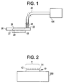
- FIG. 1 illustrates one embodiment of an exemplary multi-conductor cable 20 extending from a first electronic device 100 and terminated on one or more cable terminating PCBs 26, each having one or more cable terminating PCB surface mounted connectors 22 mounted to the PCBs 26.
- the number of cable terminating PCBs 26 and cable terminating PCB surface mounted connectors 22 can be determined by the number of required conductors in the multi-conductor cable 20.
- Each cable terminating PCB surface mounted connector 22 can be a low profile style in order to minimize the use of space extending perpendicularly from the cable terminating PCB 26.
- the individual conductors 24 of the multi-conductor cable 20 extending from the first electronic device 100 can be terminated by soldering each conductor 24 onto a first surface 25 of a cable terminating PCB 26, which has a cable terminating PCB surface mounted connector 22 on the second surface 27 of the cable terminating PCB 26.
- Each cable terminating PCB 26 can have circuits 28 to which a particular conductor 24 from the multi-conductor cable 20 is soldered and then connected to a particular electrical contact 29 of the cable terminating PCB surface mounted connector 22.
- the cable terminating PCB surface mounted connector 22 can be a male or female type.
- FIG. 2 illustrates one embodiment of an exemplary PGA connector 10 of a second electronic device 200.
- a PGA connector 10 can have a pin grid 11 with a plurality of electrical contacts in the form of pins 12. These pins 12 extend in a direction parallel to each other, perpendicularly from a first surface 14 of the PGA connector 10.
- the pins 12 can vary in number and be arranged in various geometries and configurations (e.g., certain number of rows and columns) to form a variety of pin grids 11.
- the pins 12 for two different PGA connectors can be arranged with different quantities and center-to-center spacings (e.g., spaced 0.100 inches (2.54 mm) or .050 inches (1.27 mm)).
- the particular PGA connector 10 illustrated in FIG. 1 is referenced herein throughout to illustrate the present invention, which can be modified in order to accommodate various configurations and specifications of PGA connectors 10 different from the one illustrated herein.
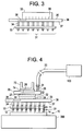
- FIG. 3 illustrates one embodiment of an exemplary connector interfacing PCB 36 having one or more connector interfacing PCB surface mounted connectors 32 mounted to a first surface 35 for mating with the cable terminating PCB surface mounted connectors 22, and one or more connector interfacing PCB surface mounted socket grid arrays 33 mounted to a second surface 37 for mating with the PGA connector 10 of the second electronic device 200.
- the number of connector interfacing PCBs 36, cable terminating PCB surface mounted connectors 32, and connector interfacing PCB surface mounted socket grid arrays 33 can be determined by the number of required conductors in the multi-conductor cable 20 or the number of pins 12 on the PGA connector 10.
- Each connector interfacing PCB surface mounted connector 32 can be a low profile style in order to minimize the use of space extending perpendicularly from the connector interfacing PCB 36.
- Each connector interfacing PCB surface mounted socket grid arrays 33 can have a socket grid 31 with a plurality of electrical contacts in the form of sockets 34, which have interior electrical contacts. These sockets 34 extend in a direction parallel to each other, perpendicularly from the second surface 37 of the connector interfacing PCB 36.
- the sockets 34 can vary in number, and be arranged in various geometries and configurations to form a variety of socket grids 31 to mate with the pin grids 11 of the PGA connector 10 of the second electronic device 200.
- the individual sockets 34 of the connector interfacing PCB surface mounted socket grid arrays 33 can be soldered onto the second surface 37 of a connector interfacing PCB 36, which has a connector interfacing PCB surface mounted connector 32 on the first surface 35 of the connector interfacing PCB 36. Furthermore, to provide extra support or adherence between the connector interfacing PCB surface mounted socket grid arrays 33 and the second surface 37, epoxy can be applied at the contact between the sockets 34 and second surface 37, or more extensively between the socket grid arrays 33 and the second surface 37. Extra support or adherence might be necessary, for instance, to accommodate any difference between the thermal expansion coefficients of the materials on either side of the union, including any solder used.
- CTE coefficient of thermal expansion
- a stage or B stage epoxy can provide extra support to the joint. This support can also provide protection against other physical stressors, including but not limited to vibration, impact, and other physical shock.
- Each cable terminating PCB 36 can have circuits 38 to which a particular socket 34 of the connector interfacing PCB surface mounted socket grid array 33 is soldered and then connected to a particular electrical contact 39 of the connector interfacing PCB surface mounted connector 32.
- the connector interfacing PCB surface mounted connectors 32 can be a male or female type in order to mate with the particular configuration of the cable terminating PCB surface mounted connectors 22.
- FIG. 4 illustrates one embodiment of the exemplary connector interfacing PCB 36 interfacing the cable terminating PCB surface mounted connectors 22 to the PGA connector 10 of the second electronic device 200 via the connectors and circuits on the connector interfacing PCB 36.
- the pins 12 of the PGA connector 10 of the second electronic device 200 are inserted into the sockets 34 of the connector interfacing PCB surface mounted socket grid array 33, which are connected to a particular electrical contact of the connector interfacing PCB surface mounted connector 32, which is mated with a particular electrical contact of the cable terminating PCB surface mounted connector 22, which is connected to a particular conductor 24 from the multi-conductor cable 20, which extends from the first electronic device 100.
- a support device 70 (e.g., a clamp or bracket) can be used as shown in FIG. 4 .
- the support device 70 can be placed in position on top of each cable terminating PCB surface mounted connector 22 and fixed to a housing (not shown) or otherwise held firmly against each cable terminating PCB surface mounted connector 22.
- the support device 70 can be made of metal, plastic, or any semi-rigid or rigid material. For example, aluminum can be used based on its light weight and malleability.
- a pad 74 can be placed between the support device 70 and the top of each cable terminating PCB surface mounted connector 22. This pad 74 (e.g., a sponge, soft foam, or other cushioning material) can protect the electrical components from being damaged by contact or pressure against the bottom surface of the support device 70, which can be hard or abrasive.
Claims (8)
- Appareil permettant de connecter un câble multiconducteur (20) à un connecteur de grille de broches (10), comprenant :une première carte à circuits imprimés (26) comprenant une première pluralité de circuits (28) connectés à une pluralité de conducteurs (24) tirés dudit câble multiconducteur (20) ;un connecteur (22) monté à la surface de la première carte à circuits imprimés, qui est monté sur ladite première carte à circuits imprimés (26), dans lequel ledit connecteur (22) monté à la surface de la première carte à circuits imprimés comprend une première pluralité de contacts électriques (29) connectés à ladite première pluralité de circuits (28) et à ladite pluralité de conducteurs (24) tirés dudit câble multiconducteur (20) via ladite première pluralité de circuits (28) ;une seconde carte à circuits imprimés (36) comprenant une seconde pluralité de circuits (38) ;un connecteur (32) monté à la surface de la seconde carte à circuits imprimés, qui est monté sur ladite seconde carte à circuits imprimés (36) et apparié audit connecteur (22) monté à la surface de la première carte à circuits imprimés, dans lequel ledit connecteur (32) monté à la surface de la seconde carte à circuits imprimés comprend une seconde pluralité de contacts électriques (39) appariés à ladite première pluralité de contacts électriques (29) et connectés à ladite seconde pluralité de circuits (38) ; etune grille de douilles (33) montée à la surface de la carte à circuits imprimés qui est montée sur ladite seconde carte à circuits imprimés (36) pour s'apparier audit connecteur de grille de broches (10), dans lequel ladite grille de douilles (33) montée à la surface de la carte à circuits imprimés comprend une pluralité de douilles (34) connectées à ladite seconde pluralité de circuits (38) et à ladite seconde pluralité de contacts électriques (39) via ladite seconde pluralité de circuits (38).
- Appareil selon la revendication 1, dans lequel ladite première pluralité de circuits (28) sont connectés à ladite pluralité de conducteurs (24) tirés dudit câble multiconducteur (20) par brasage de ladite pluralité de conducteurs (24) à ladite première pluralité de circuits (28).
- Appareil selon la revendication 1 ou 2, dans lequel ladite seconde pluralité de circuits (38) sont connectés à ladite pluralité de douilles (34) par brasage de ladite pluralité de douilles (34) à ladite seconde pluralité de circuits (38).
- Appareil selon la revendication 3, comprenant en outre une résine époxyde entre ladite grille de douilles (33) montée à la surface de la carte à circuits imprimés et la seconde carte à circuits imprimés (36).
- Appareil selon l'une quelconque des revendications précédentes, comprenant en outre :un boîtier ; etun dispositif de support (70) fixé audit boîtier et positionné contre ledit connecteur (22) monté à la surface de la première carte à circuits imprimés.
- Appareil selon la revendication 5, comprenant en outre une plaquette (74) entre ledit dispositif de support (70) et ledit connecteur (22) monté à la surface de la carte à circuits imprimés.
- Appareil selon la revendication 5, dans lequel ledit dispositif de support (70) est une pince ou une potence.
- Appareil selon l'une quelconque des revendications précédentes, dans lequel le connecteur (22) monté à la surface de ladite première carte à circuits imprimés et le connecteur (32) monté à la surface de ladite seconde carte à circuits imprimés sont des connecteurs du type à profil bas.
Applications Claiming Priority (1)
| Application Number | Priority Date | Filing Date | Title |
|---|---|---|---|
| US12/566,923 US8007288B2 (en) | 2009-09-25 | 2009-09-25 | Apparatus for connecting a multi-conductor cable to a pin grid array connector |
Publications (3)
| Publication Number | Publication Date |
|---|---|
| EP2306592A2 EP2306592A2 (fr) | 2011-04-06 |
| EP2306592A3 EP2306592A3 (fr) | 2015-01-21 |
| EP2306592B1 true EP2306592B1 (fr) | 2016-02-17 |
Family
ID=43128211
Family Applications (1)
| Application Number | Title | Priority Date | Filing Date |
|---|---|---|---|
| EP10179549.0A Active EP2306592B1 (fr) | 2009-09-25 | 2010-09-24 | Appareil pour connecter un câble multiconducteur à un connecteur de réseau de grille à broche |
Country Status (5)
| Country | Link |
|---|---|
| US (1) | US8007288B2 (fr) |
| EP (1) | EP2306592B1 (fr) |
| JP (1) | JP5681423B2 (fr) |
| CN (1) | CN102035112B (fr) |
| CA (1) | CA2714539C (fr) |
Families Citing this family (7)
| Publication number | Priority date | Publication date | Assignee | Title |
|---|---|---|---|---|
| US8007288B2 (en) * | 2009-09-25 | 2011-08-30 | Ge Inspection Technologies, Lp. | Apparatus for connecting a multi-conductor cable to a pin grid array connector |
| US9674954B2 (en) | 2013-03-14 | 2017-06-06 | Intel Corporation | Chip package connector assembly |
| CN204030038U (zh) * | 2013-03-25 | 2014-12-17 | 富加宜(亚洲)私人有限公司 | 电缆连接器组件和包括电缆连接器组件的电连接器系统 |
| WO2019055911A1 (fr) | 2017-09-15 | 2019-03-21 | Molex, Llc | Système de connecteur de boîtier matriciel |
| US11205867B2 (en) | 2017-09-15 | 2021-12-21 | Molex, Llc | Grid array connector system |
| KR20190091970A (ko) * | 2018-01-30 | 2019-08-07 | 주식회사 엘지화학 | 커넥터 피치 변경용 어댑터 및 그 제조 방법 |
| US10993325B2 (en) * | 2019-07-31 | 2021-04-27 | Abb Power Electronics Inc. | Interposer printed circuit boards for power modules |
Family Cites Families (15)
| Publication number | Priority date | Publication date | Assignee | Title |
|---|---|---|---|---|
| US5038467A (en) | 1989-11-09 | 1991-08-13 | Advanced Interconnections Corporation | Apparatus and method for installation of multi-pin components on circuit boards |
| US5313021A (en) | 1992-09-18 | 1994-05-17 | Aptix Corporation | Circuit board for high pin count surface mount pin grid arrays |
| JPH06333652A (ja) * | 1993-05-24 | 1994-12-02 | Sumitomo Electric Ind Ltd | 電子部品用端子ピッチ変換コネクタ |
| DE69409453T2 (de) * | 1993-08-31 | 1998-11-12 | Advanced Micro Devices Inc | Gerät zur Veränderung eines elektrischen Signals |
| US5813881A (en) * | 1994-02-08 | 1998-09-29 | Prolinx Labs Corporation | Programmable cable and cable adapter using fuses and antifuses |
| US5850691A (en) | 1995-07-20 | 1998-12-22 | Dell Usa, L. P. | Method for securing an electronic component to a pin grid array socket |
| JP3820603B2 (ja) * | 1995-09-28 | 2006-09-13 | Jsr株式会社 | コネクター装置 |
| US5702255A (en) | 1995-11-03 | 1997-12-30 | Advanced Interconnections Corporation | Ball grid array socket assembly |
| US6906544B1 (en) * | 2003-02-14 | 2005-06-14 | Cisco Technology, Inc. | Methods and apparatus for testing a circuit board using a surface mountable adaptor |
| US7005742B2 (en) | 2004-02-05 | 2006-02-28 | Texas Instruments Incorporated | Socket grid array |
| KR100564620B1 (ko) * | 2004-03-31 | 2006-03-29 | 삼성전자주식회사 | 열방출 특성을 개선한 메모리 모듈, 메모리 모듈용 소켓및 이를 이용한 메모리 모듈용 소켓 사용방법 |
| US7438581B1 (en) | 2005-05-16 | 2008-10-21 | Myoungsoo Jeon | Socket having printed circuit board body portion |
| EP1835295A1 (fr) * | 2006-03-17 | 2007-09-19 | 3M Innovative Properties Company | Connecteur de test, kit et procédé de distinction entre un groupe de fil et d'autres fils dans un câble à plusieurs fils |
| JP5385631B2 (ja) * | 2009-02-17 | 2014-01-08 | 矢崎総業株式会社 | ピッチ変換コネクタ |
| US8007288B2 (en) * | 2009-09-25 | 2011-08-30 | Ge Inspection Technologies, Lp. | Apparatus for connecting a multi-conductor cable to a pin grid array connector |
-
2009
- 2009-09-25 US US12/566,923 patent/US8007288B2/en active Active
-
2010
- 2010-09-09 CA CA2714539A patent/CA2714539C/fr active Active
- 2010-09-24 EP EP10179549.0A patent/EP2306592B1/fr active Active
- 2010-09-24 JP JP2010212960A patent/JP5681423B2/ja not_active Expired - Fee Related
- 2010-09-25 CN CN2010105069560A patent/CN102035112B/zh active Active
Also Published As
| Publication number | Publication date |
|---|---|
| JP5681423B2 (ja) | 2015-03-11 |
| US20110076863A1 (en) | 2011-03-31 |
| CA2714539A1 (fr) | 2011-03-25 |
| CA2714539C (fr) | 2012-11-13 |
| JP2011082157A (ja) | 2011-04-21 |
| EP2306592A2 (fr) | 2011-04-06 |
| US8007288B2 (en) | 2011-08-30 |
| CN102035112B (zh) | 2013-07-03 |
| EP2306592A3 (fr) | 2015-01-21 |
| CN102035112A (zh) | 2011-04-27 |
Similar Documents
| Publication | Publication Date | Title |
|---|---|---|
| EP2306592B1 (fr) | Appareil pour connecter un câble multiconducteur à un connecteur de réseau de grille à broche | |
| US7714569B2 (en) | Adaptor for electrical connector | |
| KR20020061122A (ko) | 차동 및 단종단 전송장치용 고속, 고밀도 인터커넥트 시스템 | |
| WO2006018958A1 (fr) | Connecteur, carte de circuit imprime, dispositif de connexion de ces elements et procedes de test de pieces electroniques utilisant ceux-ci | |
| KR20080014087A (ko) | 커넥터, 회로 기판 및 전자 기기 | |
| JP2007017234A (ja) | 検査装置用ソケット | |
| US7503769B2 (en) | Connector and pushing jig | |
| US9033740B2 (en) | Interposer connectors | |
| US20090298327A1 (en) | Connecting module | |
| US20100195302A1 (en) | Flexible guiding module | |
| JP5771614B2 (ja) | プリント回路基板コネクタ及び回路基板アセンブリ | |
| US6599143B1 (en) | Variably positionable electrical connector | |
| US20080045045A1 (en) | High density electrical connector and method for assembling thereof | |
| JP4002935B2 (ja) | デバイスインターフェース装置 | |
| RU2319263C1 (ru) | Контактирующее устройство для электрического соединения жестких печатных плат | |
| JP6448399B2 (ja) | 電子機器 | |
| US7354305B2 (en) | Area array device test adapter | |
| JPH11149953A (ja) | 電子機器 | |
| JP4962786B2 (ja) | 半導体試験装置 | |
| JP2007242561A (ja) | コネクタ構造体 | |
| JP2009193677A (ja) | アダプタ、ソケット、電子装置および実装方法 | |
| EP2876739B1 (fr) | Système d'interconnexion de ressort liga haute performance pour sonder une application | |
| US20090026345A1 (en) | Electronic device shock-absorbing mounting system | |
| CN219016383U (zh) | 匹配浮动界面的连接装置、连接器以及测试机 | |
| JP3148239U (ja) | 両端配置のマイクロ電子コネクタ |
Legal Events
| Date | Code | Title | Description |
|---|---|---|---|
| PUAI | Public reference made under article 153(3) epc to a published international application that has entered the european phase |
Free format text: ORIGINAL CODE: 0009012 |
|
| AK | Designated contracting states |
Kind code of ref document: A2 Designated state(s): AL AT BE BG CH CY CZ DE DK EE ES FI FR GB GR HR HU IE IS IT LI LT LU LV MC MK MT NL NO PL PT RO SE SI SK SM TR |
|
| AX | Request for extension of the european patent |
Extension state: BA ME RS |
|
| PUAL | Search report despatched |
Free format text: ORIGINAL CODE: 0009013 |
|
| AK | Designated contracting states |
Kind code of ref document: A3 Designated state(s): AL AT BE BG CH CY CZ DE DK EE ES FI FR GB GR HR HU IE IS IT LI LT LU LV MC MK MT NL NO PL PT RO SE SI SK SM TR |
|
| AX | Request for extension of the european patent |
Extension state: BA ME RS |
|
| RIC1 | Information provided on ipc code assigned before grant |
Ipc: H01R 12/70 20110101ALI20141218BHEP Ipc: H01R 12/71 20110101AFI20141218BHEP Ipc: G01N 29/26 20060101ALN20141218BHEP Ipc: H01R 31/06 20060101ALN20141218BHEP Ipc: H05K 1/14 20060101ALN20141218BHEP Ipc: G01R 1/04 20060101ALN20141218BHEP |
|
| 17P | Request for examination filed |
Effective date: 20150721 |
|
| RBV | Designated contracting states (corrected) |
Designated state(s): AL AT BE BG CH CY CZ DE DK EE ES FI FR GB GR HR HU IE IS IT LI LT LU LV MC MK MT NL NO PL PT RO SE SI SK SM TR |
|
| GRAP | Despatch of communication of intention to grant a patent |
Free format text: ORIGINAL CODE: EPIDOSNIGR1 |
|
| RIC1 | Information provided on ipc code assigned before grant |
Ipc: G01N 29/26 20060101ALN20150825BHEP Ipc: H01R 12/71 20110101AFI20150825BHEP Ipc: G01R 1/04 20060101ALN20150825BHEP Ipc: H01R 31/06 20060101ALN20150825BHEP Ipc: H05K 1/14 20060101ALN20150825BHEP Ipc: H01R 12/70 20110101ALI20150825BHEP |
|
| INTG | Intention to grant announced |
Effective date: 20150916 |
|
| GRAS | Grant fee paid |
Free format text: ORIGINAL CODE: EPIDOSNIGR3 |
|
| GRAA | (expected) grant |
Free format text: ORIGINAL CODE: 0009210 |
|
| AK | Designated contracting states |
Kind code of ref document: B1 Designated state(s): AL AT BE BG CH CY CZ DE DK EE ES FI FR GB GR HR HU IE IS IT LI LT LU LV MC MK MT NL NO PL PT RO SE SI SK SM TR |
|
| REG | Reference to a national code |
Ref country code: GB Ref legal event code: FG4D |
|
| REG | Reference to a national code |
Ref country code: CH Ref legal event code: EP |
|
| REG | Reference to a national code |
Ref country code: IE Ref legal event code: FG4D |
|
| REG | Reference to a national code |
Ref country code: AT Ref legal event code: REF Ref document number: 776011 Country of ref document: AT Kind code of ref document: T Effective date: 20160315 |
|
| REG | Reference to a national code |
Ref country code: DE Ref legal event code: R096 Ref document number: 602010030651 Country of ref document: DE |
|
| REG | Reference to a national code |
Ref country code: NL Ref legal event code: MP Effective date: 20160217 |
|
| REG | Reference to a national code |
Ref country code: LT Ref legal event code: MG4D |
|
| REG | Reference to a national code |
Ref country code: AT Ref legal event code: MK05 Ref document number: 776011 Country of ref document: AT Kind code of ref document: T Effective date: 20160217 |
|
| PG25 | Lapsed in a contracting state [announced via postgrant information from national office to epo] |
Ref country code: FI Free format text: LAPSE BECAUSE OF FAILURE TO SUBMIT A TRANSLATION OF THE DESCRIPTION OR TO PAY THE FEE WITHIN THE PRESCRIBED TIME-LIMIT Effective date: 20160217 Ref country code: GR Free format text: LAPSE BECAUSE OF FAILURE TO SUBMIT A TRANSLATION OF THE DESCRIPTION OR TO PAY THE FEE WITHIN THE PRESCRIBED TIME-LIMIT Effective date: 20160518 Ref country code: ES Free format text: LAPSE BECAUSE OF FAILURE TO SUBMIT A TRANSLATION OF THE DESCRIPTION OR TO PAY THE FEE WITHIN THE PRESCRIBED TIME-LIMIT Effective date: 20160217 Ref country code: IT Free format text: LAPSE BECAUSE OF FAILURE TO SUBMIT A TRANSLATION OF THE DESCRIPTION OR TO PAY THE FEE WITHIN THE PRESCRIBED TIME-LIMIT Effective date: 20160217 Ref country code: NO Free format text: LAPSE BECAUSE OF FAILURE TO SUBMIT A TRANSLATION OF THE DESCRIPTION OR TO PAY THE FEE WITHIN THE PRESCRIBED TIME-LIMIT Effective date: 20160517 |
|
| PG25 | Lapsed in a contracting state [announced via postgrant information from national office to epo] |
Ref country code: SE Free format text: LAPSE BECAUSE OF FAILURE TO SUBMIT A TRANSLATION OF THE DESCRIPTION OR TO PAY THE FEE WITHIN THE PRESCRIBED TIME-LIMIT Effective date: 20160217 Ref country code: LV Free format text: LAPSE BECAUSE OF FAILURE TO SUBMIT A TRANSLATION OF THE DESCRIPTION OR TO PAY THE FEE WITHIN THE PRESCRIBED TIME-LIMIT Effective date: 20160217 Ref country code: NL Free format text: LAPSE BECAUSE OF FAILURE TO SUBMIT A TRANSLATION OF THE DESCRIPTION OR TO PAY THE FEE WITHIN THE PRESCRIBED TIME-LIMIT Effective date: 20160217 Ref country code: PL Free format text: LAPSE BECAUSE OF FAILURE TO SUBMIT A TRANSLATION OF THE DESCRIPTION OR TO PAY THE FEE WITHIN THE PRESCRIBED TIME-LIMIT Effective date: 20160217 Ref country code: PT Free format text: LAPSE BECAUSE OF FAILURE TO SUBMIT A TRANSLATION OF THE DESCRIPTION OR TO PAY THE FEE WITHIN THE PRESCRIBED TIME-LIMIT Effective date: 20160617 Ref country code: LT Free format text: LAPSE BECAUSE OF FAILURE TO SUBMIT A TRANSLATION OF THE DESCRIPTION OR TO PAY THE FEE WITHIN THE PRESCRIBED TIME-LIMIT Effective date: 20160217 Ref country code: AT Free format text: LAPSE BECAUSE OF FAILURE TO SUBMIT A TRANSLATION OF THE DESCRIPTION OR TO PAY THE FEE WITHIN THE PRESCRIBED TIME-LIMIT Effective date: 20160217 |
|
| REG | Reference to a national code |
Ref country code: FR Ref legal event code: PLFP Year of fee payment: 7 |
|
| PG25 | Lapsed in a contracting state [announced via postgrant information from national office to epo] |
Ref country code: DK Free format text: LAPSE BECAUSE OF FAILURE TO SUBMIT A TRANSLATION OF THE DESCRIPTION OR TO PAY THE FEE WITHIN THE PRESCRIBED TIME-LIMIT Effective date: 20160217 Ref country code: EE Free format text: LAPSE BECAUSE OF FAILURE TO SUBMIT A TRANSLATION OF THE DESCRIPTION OR TO PAY THE FEE WITHIN THE PRESCRIBED TIME-LIMIT Effective date: 20160217 |
|
| REG | Reference to a national code |
Ref country code: DE Ref legal event code: R097 Ref document number: 602010030651 Country of ref document: DE |
|
| PG25 | Lapsed in a contracting state [announced via postgrant information from national office to epo] |
Ref country code: SK Free format text: LAPSE BECAUSE OF FAILURE TO SUBMIT A TRANSLATION OF THE DESCRIPTION OR TO PAY THE FEE WITHIN THE PRESCRIBED TIME-LIMIT Effective date: 20160217 Ref country code: CZ Free format text: LAPSE BECAUSE OF FAILURE TO SUBMIT A TRANSLATION OF THE DESCRIPTION OR TO PAY THE FEE WITHIN THE PRESCRIBED TIME-LIMIT Effective date: 20160217 Ref country code: SM Free format text: LAPSE BECAUSE OF FAILURE TO SUBMIT A TRANSLATION OF THE DESCRIPTION OR TO PAY THE FEE WITHIN THE PRESCRIBED TIME-LIMIT Effective date: 20160217 Ref country code: RO Free format text: LAPSE BECAUSE OF FAILURE TO SUBMIT A TRANSLATION OF THE DESCRIPTION OR TO PAY THE FEE WITHIN THE PRESCRIBED TIME-LIMIT Effective date: 20160217 |
|
| PLBE | No opposition filed within time limit |
Free format text: ORIGINAL CODE: 0009261 |
|
| STAA | Information on the status of an ep patent application or granted ep patent |
Free format text: STATUS: NO OPPOSITION FILED WITHIN TIME LIMIT |
|
| PG25 | Lapsed in a contracting state [announced via postgrant information from national office to epo] |
Ref country code: BE Free format text: LAPSE BECAUSE OF FAILURE TO SUBMIT A TRANSLATION OF THE DESCRIPTION OR TO PAY THE FEE WITHIN THE PRESCRIBED TIME-LIMIT Effective date: 20160217 |
|
| 26N | No opposition filed |
Effective date: 20161118 |
|
| PG25 | Lapsed in a contracting state [announced via postgrant information from national office to epo] |
Ref country code: SI Free format text: LAPSE BECAUSE OF FAILURE TO SUBMIT A TRANSLATION OF THE DESCRIPTION OR TO PAY THE FEE WITHIN THE PRESCRIBED TIME-LIMIT Effective date: 20160217 Ref country code: BG Free format text: LAPSE BECAUSE OF FAILURE TO SUBMIT A TRANSLATION OF THE DESCRIPTION OR TO PAY THE FEE WITHIN THE PRESCRIBED TIME-LIMIT Effective date: 20160517 |
|
| PG25 | Lapsed in a contracting state [announced via postgrant information from national office to epo] |
Ref country code: MC Free format text: LAPSE BECAUSE OF FAILURE TO SUBMIT A TRANSLATION OF THE DESCRIPTION OR TO PAY THE FEE WITHIN THE PRESCRIBED TIME-LIMIT Effective date: 20160217 |
|
| REG | Reference to a national code |
Ref country code: CH Ref legal event code: PL |
|
| GBPC | Gb: european patent ceased through non-payment of renewal fee |
Effective date: 20160924 |
|
| REG | Reference to a national code |
Ref country code: IE Ref legal event code: MM4A |
|
| PG25 | Lapsed in a contracting state [announced via postgrant information from national office to epo] |
Ref country code: CH Free format text: LAPSE BECAUSE OF NON-PAYMENT OF DUE FEES Effective date: 20160930 Ref country code: GB Free format text: LAPSE BECAUSE OF NON-PAYMENT OF DUE FEES Effective date: 20160924 Ref country code: IE Free format text: LAPSE BECAUSE OF NON-PAYMENT OF DUE FEES Effective date: 20160924 Ref country code: LI Free format text: LAPSE BECAUSE OF NON-PAYMENT OF DUE FEES Effective date: 20160930 |
|
| PG25 | Lapsed in a contracting state [announced via postgrant information from national office to epo] |
Ref country code: LU Free format text: LAPSE BECAUSE OF NON-PAYMENT OF DUE FEES Effective date: 20160924 |
|
| REG | Reference to a national code |
Ref country code: FR Ref legal event code: PLFP Year of fee payment: 8 |
|
| PG25 | Lapsed in a contracting state [announced via postgrant information from national office to epo] |
Ref country code: CY Free format text: LAPSE BECAUSE OF FAILURE TO SUBMIT A TRANSLATION OF THE DESCRIPTION OR TO PAY THE FEE WITHIN THE PRESCRIBED TIME-LIMIT Effective date: 20160217 Ref country code: HU Free format text: LAPSE BECAUSE OF FAILURE TO SUBMIT A TRANSLATION OF THE DESCRIPTION OR TO PAY THE FEE WITHIN THE PRESCRIBED TIME-LIMIT; INVALID AB INITIO Effective date: 20100924 |
|
| PG25 | Lapsed in a contracting state [announced via postgrant information from national office to epo] |
Ref country code: MK Free format text: LAPSE BECAUSE OF FAILURE TO SUBMIT A TRANSLATION OF THE DESCRIPTION OR TO PAY THE FEE WITHIN THE PRESCRIBED TIME-LIMIT Effective date: 20160217 Ref country code: TR Free format text: LAPSE BECAUSE OF FAILURE TO SUBMIT A TRANSLATION OF THE DESCRIPTION OR TO PAY THE FEE WITHIN THE PRESCRIBED TIME-LIMIT Effective date: 20160217 Ref country code: IS Free format text: LAPSE BECAUSE OF FAILURE TO SUBMIT A TRANSLATION OF THE DESCRIPTION OR TO PAY THE FEE WITHIN THE PRESCRIBED TIME-LIMIT Effective date: 20160217 Ref country code: HR Free format text: LAPSE BECAUSE OF FAILURE TO SUBMIT A TRANSLATION OF THE DESCRIPTION OR TO PAY THE FEE WITHIN THE PRESCRIBED TIME-LIMIT Effective date: 20160217 Ref country code: MT Free format text: LAPSE BECAUSE OF NON-PAYMENT OF DUE FEES Effective date: 20160930 |
|
| REG | Reference to a national code |
Ref country code: FR Ref legal event code: PLFP Year of fee payment: 9 |
|
| PG25 | Lapsed in a contracting state [announced via postgrant information from national office to epo] |
Ref country code: AL Free format text: LAPSE BECAUSE OF FAILURE TO SUBMIT A TRANSLATION OF THE DESCRIPTION OR TO PAY THE FEE WITHIN THE PRESCRIBED TIME-LIMIT Effective date: 20160217 |
|
| PGFP | Annual fee paid to national office [announced via postgrant information from national office to epo] |
Ref country code: DE Payment date: 20220818 Year of fee payment: 13 |
|
| PGFP | Annual fee paid to national office [announced via postgrant information from national office to epo] |
Ref country code: FR Payment date: 20230822 Year of fee payment: 14 |