EP2304451B1 - Verfahren zur erhöhung der esd-pulsstabilität eines elektrischen bauelements - Google Patents
Verfahren zur erhöhung der esd-pulsstabilität eines elektrischen bauelements Download PDFInfo
- Publication number
- EP2304451B1 EP2304451B1 EP09780646.7A EP09780646A EP2304451B1 EP 2304451 B1 EP2304451 B1 EP 2304451B1 EP 09780646 A EP09780646 A EP 09780646A EP 2304451 B1 EP2304451 B1 EP 2304451B1
- Authority
- EP
- European Patent Office
- Prior art keywords
- pulse
- ageing
- electrical component
- varistor
- component
- Prior art date
- Legal status (The legal status is an assumption and is not a legal conclusion. Google has not performed a legal analysis and makes no representation as to the accuracy of the status listed.)
- Not-in-force
Links
- 238000000034 method Methods 0.000 title claims description 21
- 230000032683 aging Effects 0.000 claims description 47
- 230000015556 catabolic process Effects 0.000 claims description 10
- 238000006731 degradation reaction Methods 0.000 claims description 10
- 230000001419 dependent effect Effects 0.000 description 5
- 230000003466 anti-cipated effect Effects 0.000 description 4
- 230000001052 transient effect Effects 0.000 description 4
- 239000000919 ceramic Substances 0.000 description 2
- 230000006978 adaptation Effects 0.000 description 1
- 238000011161 development Methods 0.000 description 1
- 230000018109 developmental process Effects 0.000 description 1
- 238000010586 diagram Methods 0.000 description 1
- 239000000463 material Substances 0.000 description 1
- 230000000630 rising effect Effects 0.000 description 1
Images
Classifications
-
- H—ELECTRICITY
- H10—SEMICONDUCTOR DEVICES; ELECTRIC SOLID-STATE DEVICES NOT OTHERWISE PROVIDED FOR
- H10D—INORGANIC ELECTRIC SEMICONDUCTOR DEVICES
- H10D84/00—Integrated devices formed in or on semiconductor substrates that comprise only semiconducting layers, e.g. on Si wafers or on GaAs-on-Si wafers
-
- H—ELECTRICITY
- H01—ELECTRIC ELEMENTS
- H01C—RESISTORS
- H01C7/00—Non-adjustable resistors formed as one or more layers or coatings; Non-adjustable resistors made from powdered conducting material or powdered semi-conducting material with or without insulating material
- H01C7/10—Non-adjustable resistors formed as one or more layers or coatings; Non-adjustable resistors made from powdered conducting material or powdered semi-conducting material with or without insulating material voltage responsive, i.e. varistors
-
- H—ELECTRICITY
- H01—ELECTRIC ELEMENTS
- H01C—RESISTORS
- H01C7/00—Non-adjustable resistors formed as one or more layers or coatings; Non-adjustable resistors made from powdered conducting material or powdered semi-conducting material with or without insulating material
- H01C7/02—Non-adjustable resistors formed as one or more layers or coatings; Non-adjustable resistors made from powdered conducting material or powdered semi-conducting material with or without insulating material having positive temperature coefficient
-
- H—ELECTRICITY
- H01—ELECTRIC ELEMENTS
- H01C—RESISTORS
- H01C7/00—Non-adjustable resistors formed as one or more layers or coatings; Non-adjustable resistors made from powdered conducting material or powdered semi-conducting material with or without insulating material
- H01C7/04—Non-adjustable resistors formed as one or more layers or coatings; Non-adjustable resistors made from powdered conducting material or powdered semi-conducting material with or without insulating material having negative temperature coefficient
-
- H—ELECTRICITY
- H03—ELECTRONIC CIRCUITRY
- H03K—PULSE TECHNIQUE
- H03K5/00—Manipulating of pulses not covered by one of the other main groups of this subclass
- H03K5/01—Shaping pulses
- H03K5/12—Shaping pulses by steepening leading or trailing edges
Definitions
- the publication US 2004/0239346 A1 relates to a method for determining a current / voltage characteristic of a component to be tested. To determine the current / voltage relationship, the component to be tested is stressed with ESD pulses of different amplitudes until the component is destroyed.
- the publication US 5,675,260 relates to a method for selecting a component design which is as robust as possible with respect to an electrostatic discharge.
- components of different structure are stressed with ESD pulses, wherein the amplitude of the pulses is changed until a component failure occurs.
- An object to be solved is to specify a method in which the ESD pulse stability of an electrical component is increased.
- a method for increasing the ESD (Electrostatic Discharge) pulse stability of an electrical component is specified.
- a provided electrical device is pre-aged by means of an aging pulse generated by a pulse generator. Due to the aging pulse, the degradation of an electrical characteristic of the device for further ESD pulses, which may occur during operation of the electrical device, reduced.
- transient voltage pulses such as ESD pulses
- ESD pulses can lead to a significant degradation of the current-voltage characteristic of electrical components.
- the components no longer reach the specifications desired by the customers.
- linear or non-linear resistors are used for the electrical component. Especially with these components, problems occur due to transient pulses, the can lead to a significant degradation of the current-voltage characteristic.
- the aging pulse Due to the aging pulse, at least one electrical parameter of the electrical component is changed.
- the aging pulse improves the ESD degradation of the electrical component.
- linear or non-linear resistors are understood, for example, varistors, discrete and integrated resistors.
- the varistor voltage may change with an ESD pulse.
- the varistor voltage represents a typical characteristic of varistors.
- a typical characteristic of non-linear resistors is, for example, the ratio of the current flowing through the resistor and the voltage applied to the resistor.
- Integrated resistors may for example be integrated in a multilayer component which has been produced by means of LTCC (Low Temperature Cofired Ceramics) technology.
- LTCC Low Temperature Cofired Ceramics
- non-linear resistors are understood as meaning, for example, temperature-dependent resistors such as NTCs or PTCs.
- NTCs or PTCs for example, an ESD pulse can change the dependence of the resistance on the temperature.
- the ESD degradation of the varistor voltage by For example, a 15 kV ESD pulse is caused, reduced by at least 35% in an unaged varistor to a maximum of 1%.
- the varistor voltage referred to here is the voltage of a varistor which drops at the varistor at a current intensity of 1 mA.
- an ESD pulse causes a change in resistance, which is anticipated by the application of an aging pulse.
- the temperature-dependent resistance characteristic is influenced by an ESD pulse.
- an aging pulse By pre-aging by means of an aging pulse, this change is anticipated.
- a pre-aging of the electrical component by the application of an aging pulse in further operation only a slight aging of the device occurs.
- the aging pulse preferably has a pulse height of about 500 V to 8000 V, the pulse having a length of about 10 ns to 1000 ns.
- the aging pulse preferably has a rise time of 0.1 ns to 10 ns. Rise time is the time the pulse takes to change its signal level between two defined intermediate values (typically 10% and 90%). The above values of the aging pulse are very much dependent on the design and materials, such as the ceramics used for the device.
- the pulse degradation of the characteristic of the electrical component is thus maintained over an aging pulse, wherein the Zielspeziquessirri the electrical Component to be adjusted in a design adaptation.
- the pulse shape of the aging pulse is preferably selected such that the component is pre-aged via the energy input of the aging pulse, but is not damaged.
- the aging caused by further use of the electrical component by transient pulses, such as ESD, is anticipated by the previously entered aging pulse, which improves the electrical specification of the component.
- the aging pulse is applied to a varistor.
- a varistor is a voltage dependent resistor which abruptly has a small resistance above a certain threshold voltage which is typical for the particular varistor.
- an electrical component which, after application of a method as described above, has a maximum ESD degradation of an electrical characteristic of 1%.
- the electrical component is a linear or non-linear resistor.
- linear or non-linear resistors for example, varistors, PTC elements, NTC elements or discrete or integrated resistors are understood.
- Integrated resistors are integrated, for example, in multilayer devices that are manufactured in LTCC technology.
- the clamping voltage of a varistor can be reduced by about 20% be, if with a varistor a pre-aging has taken place.
- the clamping voltage is to be understood as meaning the voltage drop of the varistor, which the varistor experiences at a current surge of more than 1 A.
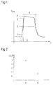
- FIG. 1 a schematic profile of an aging pulse is shown. Time is plotted on the x-axis, and the voltage of the aging pulse U p on the y-axis.
- the aging pulse preferably has a maximum pulse height 4 of approximately 500 V to 8000 V, the aging pulse rising within a time 5 of approximately 0.1 ns to 10 ns from 10% of the pulse height 1 to 90% of the pulse height 3.
- the pulse length 6 is preferably between 10 ns and 1000 ns. Pulse length 6 is the width of the pulse that the pulse has at 50% of pulse height 2.
- the aging pulse is preferably generated by means of a pulse generator.
- An electrical component is pre-pulsed with such an aging pulse.
- the electrical component is pre-aged by the aging pulse, but the component is not damaged.
- the aging which can occur during the subsequent operation of the component, is thus almost completely anticipated by the aging pulse.
- FIG. 2 shows a diagram in which the change in the varistor voltage after the application of an ESD pulse to an electrical component, in this case a varistor, is shown.
- an electrical component in this case a varistor
- the varistor voltage is the voltage of a varistor which the varistor has when introducing a current of 1 mA.
- the components are applied with aging pulse A and without aging pulse B.
- the varistor voltage at an ESD pulse of about 15 kV by at least 35%.
- the varistor voltage only drops by a maximum of 1%.
Landscapes
- Engineering & Computer Science (AREA)
- Microelectronics & Electronic Packaging (AREA)
- Physics & Mathematics (AREA)
- Electromagnetism (AREA)
- Ceramic Engineering (AREA)
- Nonlinear Science (AREA)
- Thermistors And Varistors (AREA)
- Apparatuses And Processes For Manufacturing Resistors (AREA)
- Testing Electric Properties And Detecting Electric Faults (AREA)
- Electrotherapy Devices (AREA)
Description
- Die Druckschrift
US 2004/0239346 A1 betrifft ein Verfahren zum Ermitteln einer Strom-/Spannungskennlinie eines zu testenden Bauteils. Zum Ermitteln des Strom-/Spannungszusammenhangs wird das zu testende Bauteil mit ESD-Pulsen unterschiedlicher Amplitude gestresst, bis das Bauteil zerstört ist. - Die Druckschrift
US 5,675,260 betrifft ein Verfahren zur Auswahl eines gegenüber einer elektrostatischen Entladung möglichst robusten Bauteildesigns. Dabei werden Bauteile von unterschiedlicher Struktur mit ESD-Pulsen gestresst, wobei die Amplitude der Pulse verändert wird, bis ein Bauteilversagen auftritt. - Eine zu lösende Aufgabe ist es, ein Verfahren anzugeben, bei dem die ESD-Pulsstabilität eines elektrischen Bauelements erhöht wird.
- Diese Aufgabe wird durch ein Verfahren nach Patentanspruch 1 gelöst. Vorteilhafte Ausgestaltungen des Verfahrens sind Gegenstand von Unteransprüchen.
- Es wird ein Verfahren zur Erhöhung der ESD- (Electrostatic Discharge) Pulsstabilität eines elektrischen Bauelements angegeben. Ein bereitgestelltes elektrisches Bauelement wird mittels eines Alterungspulses, der durch einen Pulsgenerator erzeugt wird, vorgealtert. Durch den Alterungspuls wird die Degradation einer elektrischen Kennlinie des Bauelements für weitere ESD-Pulse, die während des Betriebs des elektrischen Bauelements auftreten können, verringert.
- Während des Betriebs von den elektrischen Bauelementen können transiente Spannungspulse, wie beispielsweise ESD-Pulse, zu einer deutlichen Degradation der Stromspannungskennlinie von elektrischen Bauelementen führen. Durch eine Degradation der Stromspannungskennlinie erreichen die Bauelemente somit nicht mehr die von den Kunden gewünschten Spezifikationen.
- Für das elektrische Bauelement werden bevorzugt lineare oder nichtlineare Widerstände verwendet. Gerade bei diesen Bauelementen treten Probleme durch transiente Pulse auf, die zu einer deutlichen Degradation der Stromspannungskennlinie führen können.
- Durch den Alterungspuls wird wenigstens eine elektrische Kenngröße des elektrischen Bauelements verändert. Durch den Alterungspuls wird die ESD-Degradation des elektrischen Bauelements verbessert.
- Als lineare oder nichtlineare Widerstände werden beispielsweise Varistoren, diskrete und integrierte Widerstände verstanden.
- Bei einem Varistor kann sich bei einem ESD-Puls beispielsweise die Varistorspannung ändern. Die Varistorspannung stellt eine typische Kenngröße von Varistoren dar. Eine typische Kenngröße von nichtlinearen Widerständen ist beispielsweise das Verhältnis vom Strom der durch den Widerstand fließt und der Spannung die am Widerstand anliegt.
- Integrierte Widerstände können beispielsweise in einem Vielschichtbauelement integriert sein, das mittels LTCC- (Low Temperature Cofired Ceramics = Niedertemperatur-Einbrand-Keramiken) Technologie hergestellt wurde.
- Des Weiteren werden unter nichtlinearen Widerständen beispielsweise temperaturabhängige Widerstände wie NTCs oder PTCs verstanden. Bei NTCs oder PTCs kann sich durch einen ESD-Puls beispielsweise die Abhängigkeit des Widerstands von der Temperatur verändern.
- Durch den Alterungspuls wird beispielsweise bei einem Varistor die ESD-Degradation der Varistorspannung, die durch beispielsweise einen 15 kV ESD-Puls hervorgerufen wird, von wenigstens 35 % bei einem ungealterten Varistor auf maximal 1 % verringert. Als Varistorspannung wird dabei die Spannung eines Varistors bezeichnet, die an dem Varistor bei einer Stromstärke von 1 mA abfällt.
- Bei diskreten Widerständen tritt durch einen ESD-Puls eine Änderung des Widerstands auf, die durch das Beaufschlagen mit einem Alterungspuls vorweggenommen wird.
- Bei PTCs oder NTCs wird durch einen ESD-Puls die temperaturabhängige Widerstandskennlinie beeinflusst. Durch die Voralterung mittels eines Alterungspulses wird diese Veränderung vorweggenommen. Somit tritt bei einer Voralterung des elektrischen Bauelements durch das Anlegen eines Alterungspulses im weiteren Betrieb nur noch eine geringfügige Alterung des Bauelements auf.
- Der Alterungspuls weist vorzugsweise eine Pulshöhe von etwa 500 V bis 8000 V auf, wobei der Puls eine Länge von ungefähr 10 ns bis 1000 ns aufweist. Der Alterungspuls weist vorzugsweise eine Anstiegszeit von 0,1 ns bis 10 ns auf. Unter der Anstiegszeit ist die Zeit zu verstehen, die der Puls benötigt, um seinen Signalpegel zwischen zwei definierten Zwischenwerten (üblich sind 10 % und 90 %) zu ändern. Die zuvor angegebenen Werte des Alterungspulses sind sehr stark von dem Design und den Materialien, wie beispielsweise den für das Bauelement verwendeten Keramiken, abhängig.
- Die Pulsdegradation der Kennlinie des elektrischen Bauelements wird somit über einen Alterungspuls vorgehalten, wobei die Zielspezifikationswerte des elektrischen Bauelements bei einer Designanpassung eingestellt werden. Die Pulsform des Alterungspulses wird vorzugsweise derart ausgewählt, dass das Bauteil über den Energieeintrag des Alterungspulses vorgealtert, jedoch nicht geschädigt wird. Die in der weiteren Verwendung des elektrischen Bauelements hervorgerufene Alterung durch transiente Pulse, wie ESD, wird durch den zuvor eingetragenen Alterungspuls vorweggenommen, wodurch sich die elektrische Spezifikation des Bauteils verbessern.
- In einer Ausführungsform wird der Alterungspuls an einem Varistor angewandt.
- Durch den Alterungspuls wird die Varistorspannung des Varistors stabilisiert. Bei einem Varistor handelt es sich um einen spannungsabhängigen Widerstand, der oberhalb einer bestimmten Schwellspannung, die typisch für den jeweiligen Varistor ist, abrupt einen kleinen Widerstand aufweist.
- Des Weiteren wird ein elektrisches Bauelement angegeben, das nach Anwendung eines wie oben beschriebenen Verfahrens eine maximale ESD-Degradation einer elektrischen Kennlinie von 1 % aufweist. Bei dem elektrischen Bauelement handelt es sich um einen linearen oder nichtlinearen Widerstand. Unter linearen beziehungsweise nichtlinearen Widerständen werden beispielsweise Varistoren, PTC-Elemente, NTC-Elemente beziehungsweise diskrete oder integrierte Widerstände verstanden. Integrierte Widerstände werden beispielsweise in Vielschichtbauelementen integriert, die in LTCC-Technologie hergestellt sind.
- Durch ein zuvor beschriebenes Verfahren kann beispielsweise die Klemmspannung eines Varistors um ungefähr 20 % reduziert werden, falls bei einem Varistor eine Voralterung stattgefunden hat.
- Unter der Klemmspannung ist der Spannungsabfall des Varistors zu verstehen, den der Varistor bei einem Stromstoß von mehr als 1 A erfährt.
- Das oben beschriebene Verfahren und die Gegenstände werden anhand der folgenden Figuren und Ausführungsbeispiele näher erläutert.
- Die nachfolgend beschriebenen Zeichnungen sind nicht als maßstabsgetreu aufzufassen. Vielmehr können zur besseren Darstellung einzelne Dimensionen vergrößert, verkleinert oder auch verzerrt dargestellt sein. Elemente, die einander gleichen oder die die gleiche Funktion übernehmen, sind mit den gleichen Bezugszeichen bezeichnet.
-
Figur 1 zeigt ein schematisches Profil eines Alterungspulses, -
Figur 2 zeigt ein Diagramm der Varistorspannung für gealterte und ungealterte Bauteile. - In der
Figur 1 ist ein schematisches Profil eines Alterungspulses gezeigt. Auf der x-Achse ist Zeit aufgetragen, auf der y-Achse die Spannung des Alterungspulses Up. Der Alterungspuls weist vorzugsweise eine maximale Pulshöhe 4 von ungefähr 500 V bis 8000 V auf, wobei der Alterungspuls innerhalb einer Zeit 5 von ca. 0,1 ns bis 10 ns von 10% der Pulshöhe 1 auf 90% der Pulshöhe 3 ansteigt. Die Pulslänge 6 beträgt bevorzugt zwischen 10 ns und 1000 ns. Die Pulslänge 6 ist die Breite des Pulses, die der Puls bei 50% der Pulshöhe 2 aufweist. - Der Alterungspuls wird vorzugsweise mittels eines Pulsgenerators erzeugt. Ein elektrisches Bauelement wird mit einem derartigen Alterungspuls vorgepulst. Dadurch wird das elektrische Bauelement durch den Alterungspuls vorgealtert, wobei das Bauelement jedoch nicht geschädigt wird. Die Alterung, die beim nachfolgenden Betrieb des Bauelements auftreten kann, wird durch den Alterungspuls somit nahezu vollständig vorweggenommen.
- Die
Figur 2 zeigt ein Diagramm, in dem die Änderung der Varistorspannung nach dem Einwirken eines ESD-Pulses auf ein elektrisches Bauelement, in diesem Fall ein Varistor, dargestellt ist. Auf der y-Achse ist die Änderung der Varistorspannung ΔUv in Prozent dargestellt. - Als Varistorspannung wird die Spannung eines Varistors bezeichnet, die der Varistor beim Einbringen eines Stroms von 1mA aufweist.
- Auf der x-Achse sind die Bauelemente mit Alterungspuls A und ohne Alterungspuls B aufgetragen. Bei einem Bauelement B, das nicht mit einem Alterungspuls vorgealtert wurde, fällt beispielsweise wie in
Figur 2 gezeigt, die Varistorspannung bei einem ESD-Puls von ungefähr 15 kV um wenigstens 35% ab. Wenn das Bauelement A mittels eines Alterungspulses, von beispielsweise 4 kV, vorgealtert wurde, fällt die Varistorspannung dagegen nur um maximal 1% ab. - Obwohl in den Ausführungsbeispielen nur eine beschränkte Anzahl möglicher Weiterbildung der Erfindung beschrieben werden konnte ist die Erfindung nicht auf diese beschränkt. Es ist prinzipiell möglich, dass das Verfahren auch auf andere elektrische Bauelemente angewendet werden kann, die durch transiente Pulse altern.
-
- 1
- 10% Pulshöhe
- 2
- 50% Pulshöhe
- 3
- 90% Pulshöhe
- 4
- maximale Pulshöhe
- 5
- Anstiegszeit
- 6
- Pulslänge
- A
- Bauelement mit Voralterung
- B
- Bauelement ohne Voralterung
Claims (11)
- Verfahren zur Erhöhung der ESD-Pulsstabilität eines elektrischen Bauelements,- wobei von einem Pulsgenerator ein Puls erzeugt wird und ein bereitgestelltes Bauelement mit dem Puls vorgepulst wird,
dadurch gekennzeichnet, dass- der Puls ein Alterungspuls mit einer Pulsform ist, wobei die Pulsform derart gewählt ist, dass das Bauteil über den Energieeintrag des Alterungspulses vorgealtert und nicht beschädigt wird,- wodurch die Degradation einer elektrischen Kennlinie des Bauelements durch ESD-Pulse, die während des Betriebs des elektrischen Bauelements auftreten, verringert wird. - Verfahren nach Anspruch 1, wobei als elektrisches Bauelement ein linearer oder nichtlinearer Widerstand verwendet wird.
- Verfahren nach Anspruch 1, wobei wenigstens eine elektrische Kenngröße des elektrischen Bauelements durch den Alterungspuls verändert wird.
- Verfahren nach Anspruch 1, wobei das elektrische Bauelement nach Anlegen des Alterungspulses im Betrieb nur noch geringfügig altert.
- Verfahren nach Anspruch 1, wobei der Alterungspuls eine Pulshöhe von 500V bis 8000V aufweist.
- Verfahren nach Anspruch 1, wobei der Alterungspuls eine Pulslänge von 10ns bis 1000ns aufweist.
- Verfahren nach Anspruch 1, wobei der Alterungspuls eine Anstiegszeit von 0,1ns bis 10ns aufweist.
- Verfahren nach einem der Ansprüche 1 bis 7, wobei der Alterungspuls auf einen Varistor angewandt wird.
- Verfahren nach Anspruch 8, wobei der Varistor eine Varistorspannung aufweist, die durch den Alterungspuls stabilisiert wird.
- Elektrisches Bauelement, das nach Anwendung eines Verfahrens nach einem der Ansprüche 1 bis 7 eine maximale ESD-Degradation einer elektrischen Kennlinie von 1% aufweist.
- Elektrisches Bauelement nach Anspruch 10, wobei es sich um einen Varistor, ein PTC-Element oder ein NTC-Element handelt.
Applications Claiming Priority (2)
| Application Number | Priority Date | Filing Date | Title |
|---|---|---|---|
| DE102008033392.1A DE102008033392B4 (de) | 2008-07-16 | 2008-07-16 | Verfahren zur Erhöhung der ESD-Pulsstabilität eines elektrischen Bauelements |
| PCT/EP2009/059081 WO2010007102A1 (de) | 2008-07-16 | 2009-07-15 | Verfahren zur erhöhung der esd-pulsstabilität eines elektrischen bauelements |
Publications (2)
| Publication Number | Publication Date |
|---|---|
| EP2304451A1 EP2304451A1 (de) | 2011-04-06 |
| EP2304451B1 true EP2304451B1 (de) | 2016-10-19 |
Family
ID=41306164
Family Applications (1)
| Application Number | Title | Priority Date | Filing Date |
|---|---|---|---|
| EP09780646.7A Not-in-force EP2304451B1 (de) | 2008-07-16 | 2009-07-15 | Verfahren zur erhöhung der esd-pulsstabilität eines elektrischen bauelements |
Country Status (7)
| Country | Link |
|---|---|
| US (1) | US8294547B2 (de) |
| EP (1) | EP2304451B1 (de) |
| JP (1) | JP5351262B2 (de) |
| KR (1) | KR101582363B1 (de) |
| CN (1) | CN102099697B (de) |
| DE (1) | DE102008033392B4 (de) |
| WO (1) | WO2010007102A1 (de) |
Families Citing this family (2)
| Publication number | Priority date | Publication date | Assignee | Title |
|---|---|---|---|---|
| KR101923190B1 (ko) * | 2012-02-17 | 2018-11-30 | 삼성디스플레이 주식회사 | 정전기 보호 회로를 구비한 표시장치 및 그의 제조방법 |
| CN109633408B (zh) * | 2018-12-10 | 2021-05-25 | 大族激光科技产业集团股份有限公司 | 测试系统及测试方法 |
Family Cites Families (13)
| Publication number | Priority date | Publication date | Assignee | Title |
|---|---|---|---|---|
| US4080571A (en) * | 1976-06-03 | 1978-03-21 | Rca Corporation | Apparatus for measuring the current-voltage characteristics of a TRAPATT diode |
| DE3003136A1 (de) * | 1980-01-29 | 1981-07-30 | Siemens AG, 1000 Berlin und 8000 München | Verfahren zum herstellen von thermisch stabilen, metallischen schichten |
| JPH0637096A (ja) * | 1992-07-17 | 1994-02-10 | Matsushita Electric Ind Co Ltd | 薄膜のアニーリング方法 |
| JP2002164202A (ja) * | 1993-02-10 | 2002-06-07 | Seiko Epson Corp | 非線形抵抗素子およびその製造方法ならびに液晶表示装置 |
| US5410254A (en) * | 1993-03-04 | 1995-04-25 | Lsi Logic Corporation | Method for optimizing the structure of a transistor to withstand electrostatic discharge |
| US5966645A (en) * | 1997-06-03 | 1999-10-12 | Garmin Corporation | Transmitter with low-level modulation and minimal harmonic emissions |
| DE59801018D1 (de) * | 1997-09-16 | 2001-08-16 | Trench Switzerland Ag Basel | Spannungsteiler |
| US5978197A (en) * | 1997-11-18 | 1999-11-02 | Lsi Corporation | Testing ESD protection schemes in semiconductor integrated circuits |
| DE10162542A1 (de) * | 2001-12-19 | 2003-04-10 | Infineon Technologies Ag | Verfahren zum Bestimmen einer ESD-/Latch-up-Festigkeit einer integrierten Schaltung |
| EP1480046A1 (de) * | 2003-05-23 | 2004-11-24 | Interuniversitair Microelektronica Centrum ( Imec) | Verfahren zur Messung der Strom-Spannungs-Charakteristik eines Snap-Back-Bauelements |
| JP4516294B2 (ja) * | 2003-09-30 | 2010-08-04 | パナソニック株式会社 | 半導体装置及び半導体装置の製造方法 |
| EP1972952A1 (de) * | 2007-03-19 | 2008-09-24 | Interuniversitair Micro-Elektronica Centrum Vzw | Kalibrierung eines ESD-Testsystems |
| US7928737B2 (en) * | 2008-05-23 | 2011-04-19 | Hernandez Marcos | Electrical overstress and transient latch-up pulse generation system, circuit, and method |
-
2008
- 2008-07-16 DE DE102008033392.1A patent/DE102008033392B4/de not_active Expired - Fee Related
-
2009
- 2009-07-15 WO PCT/EP2009/059081 patent/WO2010007102A1/de not_active Ceased
- 2009-07-15 EP EP09780646.7A patent/EP2304451B1/de not_active Not-in-force
- 2009-07-15 JP JP2011517919A patent/JP5351262B2/ja not_active Expired - Fee Related
- 2009-07-15 CN CN200980127768.2A patent/CN102099697B/zh not_active Expired - Fee Related
- 2009-07-15 KR KR1020117003630A patent/KR101582363B1/ko not_active Expired - Fee Related
-
2011
- 2011-01-14 US US13/007,078 patent/US8294547B2/en not_active Expired - Fee Related
Also Published As
| Publication number | Publication date |
|---|---|
| EP2304451A1 (de) | 2011-04-06 |
| JP5351262B2 (ja) | 2013-11-27 |
| CN102099697B (zh) | 2016-04-20 |
| WO2010007102A1 (de) | 2010-01-21 |
| CN102099697A (zh) | 2011-06-15 |
| US8294547B2 (en) | 2012-10-23 |
| JP2011528183A (ja) | 2011-11-10 |
| KR101582363B1 (ko) | 2016-01-04 |
| DE102008033392B4 (de) | 2018-02-22 |
| US20110163842A1 (en) | 2011-07-07 |
| DE102008033392A1 (de) | 2010-01-21 |
| KR20110043673A (ko) | 2011-04-27 |
Similar Documents
| Publication | Publication Date | Title |
|---|---|---|
| EP3304671B1 (de) | Überspannungsschutzschaltung | |
| DE102007007921B4 (de) | Umrichter und Verfahren zum Betrieb | |
| EP2340593B1 (de) | Mehrstufige überspannungsschutzschaltung, insbesondere für informationstechnische anlagen | |
| DE102009041005A1 (de) | Vorrichtung zur Symmetrierung eines Energiespeichers | |
| DE102012107779A1 (de) | Elektronische Schutzvorrichtung, Verfahren zum Betreiben einer elektronischen Schutzvorrichtung sowie deren Verwendung | |
| EP3359429B1 (de) | Verfahren zum ansteuern eines elektromagnetventils und korrespondierendes fluidsystem | |
| EP2506436A2 (de) | Eingangsschaltung für eine Eingangsbaugruppe und Verfahren zum Betreiben einer Eingangsschaltung | |
| DE102008033392B4 (de) | Verfahren zur Erhöhung der ESD-Pulsstabilität eines elektrischen Bauelements | |
| DE102008007397A1 (de) | Verfahren zur Überwachung von wenigstens einer Glühstiftkerze eines Brennkraftmotors und Vorrichtung hierzu | |
| DE102012214717A1 (de) | Verfahren und Vorrichtung zur Leistungssteuerung oder Spannungssteuerung eines elektrischen Verbrauchers | |
| DE102016105506A1 (de) | Temperaturmessvorrichtung | |
| EP3108559B1 (de) | Überspannungsschutzvorrichtung mit leckstromabschaltung | |
| WO2021058302A1 (de) | Verfahren und einrichtung zum ermitteln einer eine temperatur eines widerstandstemperaturfühlers beschreibenden temperaturinformation, wechselrichter, fahrzeug und computerprogramm | |
| EP1703629A2 (de) | Verfahren zur digitalen Stromregelung | |
| DE202015102834U1 (de) | Überspannungsschutzschaltung | |
| EP2517076B1 (de) | Elektrische schaltung zum schalten und/oder dimmen von lasten | |
| DE102004039601B3 (de) | Schaltungsanordnung zum Schutz eines Leiterelements gegen Überstrom | |
| DE102007051360A1 (de) | Vorrichtung zum Betreiben einer Schaltungsanordnung | |
| DE102016218141B4 (de) | Integrierter Schaltkreis, elektronisches Steuergerät und Anordnung zur Realisierung eines elektrischen Widerstandswertes | |
| WO2005044720A1 (de) | Layoutmassnahmen zur begrenzung der ausbreitung von oberflächenrissen in mems | |
| DE19526493A1 (de) | Verfahren zur Steuerung eines Laststromkreises | |
| DE102006033925A1 (de) | Schaltungsanordnung zum Schutz vor Überspannungen | |
| DE9314632U1 (de) | Einrichtung zum Überspannungsschutz | |
| DE102012007417A1 (de) | Sensormodul | |
| EP1390668A1 (de) | Flammenüberwachungsvorrichtung |
Legal Events
| Date | Code | Title | Description |
|---|---|---|---|
| PUAI | Public reference made under article 153(3) epc to a published international application that has entered the european phase |
Free format text: ORIGINAL CODE: 0009012 |
|
| 17P | Request for examination filed |
Effective date: 20110111 |
|
| AK | Designated contracting states |
Kind code of ref document: A1 Designated state(s): AT BE BG CH CY CZ DE DK EE ES FI FR GB GR HR HU IE IS IT LI LT LU LV MC MK MT NL NO PL PT RO SE SI SK SM TR |
|
| AX | Request for extension of the european patent |
Extension state: AL BA RS |
|
| DAX | Request for extension of the european patent (deleted) | ||
| REG | Reference to a national code |
Ref country code: DE Ref legal event code: R079 Ref document number: 502009013261 Country of ref document: DE Free format text: PREVIOUS MAIN CLASS: G01R0031000000 Ipc: H01C0007020000 |
|
| GRAP | Despatch of communication of intention to grant a patent |
Free format text: ORIGINAL CODE: EPIDOSNIGR1 |
|
| RIC1 | Information provided on ipc code assigned before grant |
Ipc: H01C 7/02 20060101AFI20160504BHEP Ipc: H01C 7/04 20060101ALI20160504BHEP Ipc: H01C 7/10 20060101ALI20160504BHEP |
|
| INTG | Intention to grant announced |
Effective date: 20160531 |
|
| GRAS | Grant fee paid |
Free format text: ORIGINAL CODE: EPIDOSNIGR3 |
|
| GRAA | (expected) grant |
Free format text: ORIGINAL CODE: 0009210 |
|
| AK | Designated contracting states |
Kind code of ref document: B1 Designated state(s): AT BE BG CH CY CZ DE DK EE ES FI FR GB GR HR HU IE IS IT LI LT LU LV MC MK MT NL NO PL PT RO SE SI SK SM TR |
|
| REG | Reference to a national code |
Ref country code: GB Ref legal event code: FG4D Free format text: NOT ENGLISH |
|
| RIN1 | Information on inventor provided before grant (corrected) |
Inventor name: PUERSTINGER, THOMAS Inventor name: FEICHTINGER, THOMAS Inventor name: ALBRECHER, MARKUS Inventor name: ENGEL, GUENTER |
|
| REG | Reference to a national code |
Ref country code: CH Ref legal event code: EP |
|
| REG | Reference to a national code |
Ref country code: AT Ref legal event code: REF Ref document number: 838944 Country of ref document: AT Kind code of ref document: T Effective date: 20161115 |
|
| REG | Reference to a national code |
Ref country code: IE Ref legal event code: FG4D Free format text: LANGUAGE OF EP DOCUMENT: GERMAN |
|
| REG | Reference to a national code |
Ref country code: DE Ref legal event code: R096 Ref document number: 502009013261 Country of ref document: DE |
|
| REG | Reference to a national code |
Ref country code: NL Ref legal event code: MP Effective date: 20161019 |
|
| REG | Reference to a national code |
Ref country code: LT Ref legal event code: MG4D |
|
| PG25 | Lapsed in a contracting state [announced via postgrant information from national office to epo] |
Ref country code: LV Free format text: LAPSE BECAUSE OF FAILURE TO SUBMIT A TRANSLATION OF THE DESCRIPTION OR TO PAY THE FEE WITHIN THE PRESCRIBED TIME-LIMIT Effective date: 20161019 |
|
| PG25 | Lapsed in a contracting state [announced via postgrant information from national office to epo] |
Ref country code: NO Free format text: LAPSE BECAUSE OF FAILURE TO SUBMIT A TRANSLATION OF THE DESCRIPTION OR TO PAY THE FEE WITHIN THE PRESCRIBED TIME-LIMIT Effective date: 20170119 Ref country code: SE Free format text: LAPSE BECAUSE OF FAILURE TO SUBMIT A TRANSLATION OF THE DESCRIPTION OR TO PAY THE FEE WITHIN THE PRESCRIBED TIME-LIMIT Effective date: 20161019 Ref country code: LT Free format text: LAPSE BECAUSE OF FAILURE TO SUBMIT A TRANSLATION OF THE DESCRIPTION OR TO PAY THE FEE WITHIN THE PRESCRIBED TIME-LIMIT Effective date: 20161019 Ref country code: GR Free format text: LAPSE BECAUSE OF FAILURE TO SUBMIT A TRANSLATION OF THE DESCRIPTION OR TO PAY THE FEE WITHIN THE PRESCRIBED TIME-LIMIT Effective date: 20170120 |
|
| PG25 | Lapsed in a contracting state [announced via postgrant information from national office to epo] |
Ref country code: HR Free format text: LAPSE BECAUSE OF FAILURE TO SUBMIT A TRANSLATION OF THE DESCRIPTION OR TO PAY THE FEE WITHIN THE PRESCRIBED TIME-LIMIT Effective date: 20161019 Ref country code: ES Free format text: LAPSE BECAUSE OF FAILURE TO SUBMIT A TRANSLATION OF THE DESCRIPTION OR TO PAY THE FEE WITHIN THE PRESCRIBED TIME-LIMIT Effective date: 20161019 Ref country code: IS Free format text: LAPSE BECAUSE OF FAILURE TO SUBMIT A TRANSLATION OF THE DESCRIPTION OR TO PAY THE FEE WITHIN THE PRESCRIBED TIME-LIMIT Effective date: 20170219 Ref country code: FI Free format text: LAPSE BECAUSE OF FAILURE TO SUBMIT A TRANSLATION OF THE DESCRIPTION OR TO PAY THE FEE WITHIN THE PRESCRIBED TIME-LIMIT Effective date: 20161019 Ref country code: PT Free format text: LAPSE BECAUSE OF FAILURE TO SUBMIT A TRANSLATION OF THE DESCRIPTION OR TO PAY THE FEE WITHIN THE PRESCRIBED TIME-LIMIT Effective date: 20170220 Ref country code: NL Free format text: LAPSE BECAUSE OF FAILURE TO SUBMIT A TRANSLATION OF THE DESCRIPTION OR TO PAY THE FEE WITHIN THE PRESCRIBED TIME-LIMIT Effective date: 20161019 Ref country code: PL Free format text: LAPSE BECAUSE OF FAILURE TO SUBMIT A TRANSLATION OF THE DESCRIPTION OR TO PAY THE FEE WITHIN THE PRESCRIBED TIME-LIMIT Effective date: 20161019 |
|
| REG | Reference to a national code |
Ref country code: DE Ref legal event code: R097 Ref document number: 502009013261 Country of ref document: DE |
|
| PG25 | Lapsed in a contracting state [announced via postgrant information from national office to epo] |
Ref country code: SK Free format text: LAPSE BECAUSE OF FAILURE TO SUBMIT A TRANSLATION OF THE DESCRIPTION OR TO PAY THE FEE WITHIN THE PRESCRIBED TIME-LIMIT Effective date: 20161019 Ref country code: DK Free format text: LAPSE BECAUSE OF FAILURE TO SUBMIT A TRANSLATION OF THE DESCRIPTION OR TO PAY THE FEE WITHIN THE PRESCRIBED TIME-LIMIT Effective date: 20161019 Ref country code: EE Free format text: LAPSE BECAUSE OF FAILURE TO SUBMIT A TRANSLATION OF THE DESCRIPTION OR TO PAY THE FEE WITHIN THE PRESCRIBED TIME-LIMIT Effective date: 20161019 Ref country code: RO Free format text: LAPSE BECAUSE OF FAILURE TO SUBMIT A TRANSLATION OF THE DESCRIPTION OR TO PAY THE FEE WITHIN THE PRESCRIBED TIME-LIMIT Effective date: 20161019 Ref country code: CZ Free format text: LAPSE BECAUSE OF FAILURE TO SUBMIT A TRANSLATION OF THE DESCRIPTION OR TO PAY THE FEE WITHIN THE PRESCRIBED TIME-LIMIT Effective date: 20161019 |
|
| PLBE | No opposition filed within time limit |
Free format text: ORIGINAL CODE: 0009261 |
|
| STAA | Information on the status of an ep patent application or granted ep patent |
Free format text: STATUS: NO OPPOSITION FILED WITHIN TIME LIMIT |
|
| PG25 | Lapsed in a contracting state [announced via postgrant information from national office to epo] |
Ref country code: IT Free format text: LAPSE BECAUSE OF FAILURE TO SUBMIT A TRANSLATION OF THE DESCRIPTION OR TO PAY THE FEE WITHIN THE PRESCRIBED TIME-LIMIT Effective date: 20161019 Ref country code: BG Free format text: LAPSE BECAUSE OF FAILURE TO SUBMIT A TRANSLATION OF THE DESCRIPTION OR TO PAY THE FEE WITHIN THE PRESCRIBED TIME-LIMIT Effective date: 20170119 Ref country code: SM Free format text: LAPSE BECAUSE OF FAILURE TO SUBMIT A TRANSLATION OF THE DESCRIPTION OR TO PAY THE FEE WITHIN THE PRESCRIBED TIME-LIMIT Effective date: 20161019 |
|
| 26N | No opposition filed |
Effective date: 20170720 |
|
| PG25 | Lapsed in a contracting state [announced via postgrant information from national office to epo] |
Ref country code: SI Free format text: LAPSE BECAUSE OF FAILURE TO SUBMIT A TRANSLATION OF THE DESCRIPTION OR TO PAY THE FEE WITHIN THE PRESCRIBED TIME-LIMIT Effective date: 20161019 |
|
| REG | Reference to a national code |
Ref country code: CH Ref legal event code: PL |
|
| GBPC | Gb: european patent ceased through non-payment of renewal fee |
Effective date: 20170715 |
|
| REG | Reference to a national code |
Ref country code: IE Ref legal event code: MM4A |
|
| REG | Reference to a national code |
Ref country code: FR Ref legal event code: ST Effective date: 20180330 |
|
| PG25 | Lapsed in a contracting state [announced via postgrant information from national office to epo] |
Ref country code: IE Free format text: LAPSE BECAUSE OF NON-PAYMENT OF DUE FEES Effective date: 20170715 Ref country code: GB Free format text: LAPSE BECAUSE OF NON-PAYMENT OF DUE FEES Effective date: 20170715 Ref country code: CH Free format text: LAPSE BECAUSE OF NON-PAYMENT OF DUE FEES Effective date: 20170731 Ref country code: LI Free format text: LAPSE BECAUSE OF NON-PAYMENT OF DUE FEES Effective date: 20170731 |
|
| REG | Reference to a national code |
Ref country code: BE Ref legal event code: MM Effective date: 20170731 |
|
| PG25 | Lapsed in a contracting state [announced via postgrant information from national office to epo] |
Ref country code: FR Free format text: LAPSE BECAUSE OF NON-PAYMENT OF DUE FEES Effective date: 20170731 |
|
| PG25 | Lapsed in a contracting state [announced via postgrant information from national office to epo] |
Ref country code: LU Free format text: LAPSE BECAUSE OF NON-PAYMENT OF DUE FEES Effective date: 20170715 |
|
| PG25 | Lapsed in a contracting state [announced via postgrant information from national office to epo] |
Ref country code: BE Free format text: LAPSE BECAUSE OF NON-PAYMENT OF DUE FEES Effective date: 20170731 |
|
| REG | Reference to a national code |
Ref country code: AT Ref legal event code: MM01 Ref document number: 838944 Country of ref document: AT Kind code of ref document: T Effective date: 20170715 |
|
| PG25 | Lapsed in a contracting state [announced via postgrant information from national office to epo] |
Ref country code: MT Free format text: LAPSE BECAUSE OF FAILURE TO SUBMIT A TRANSLATION OF THE DESCRIPTION OR TO PAY THE FEE WITHIN THE PRESCRIBED TIME-LIMIT Effective date: 20161019 |
|
| REG | Reference to a national code |
Ref country code: DE Ref legal event code: R082 Ref document number: 502009013261 Country of ref document: DE Representative=s name: EPPING HERMANN FISCHER PATENTANWALTSGESELLSCHA, DE Ref country code: DE Ref legal event code: R081 Ref document number: 502009013261 Country of ref document: DE Owner name: TDK ELECTRONICS AG, DE Free format text: FORMER OWNER: EPCOS AG, 81669 MUENCHEN, DE |
|
| PG25 | Lapsed in a contracting state [announced via postgrant information from national office to epo] |
Ref country code: AT Free format text: LAPSE BECAUSE OF NON-PAYMENT OF DUE FEES Effective date: 20170715 |
|
| PG25 | Lapsed in a contracting state [announced via postgrant information from national office to epo] |
Ref country code: HU Free format text: LAPSE BECAUSE OF FAILURE TO SUBMIT A TRANSLATION OF THE DESCRIPTION OR TO PAY THE FEE WITHIN THE PRESCRIBED TIME-LIMIT; INVALID AB INITIO Effective date: 20090715 Ref country code: MC Free format text: LAPSE BECAUSE OF FAILURE TO SUBMIT A TRANSLATION OF THE DESCRIPTION OR TO PAY THE FEE WITHIN THE PRESCRIBED TIME-LIMIT Effective date: 20161019 |
|
| PG25 | Lapsed in a contracting state [announced via postgrant information from national office to epo] |
Ref country code: CY Free format text: LAPSE BECAUSE OF NON-PAYMENT OF DUE FEES Effective date: 20161019 |
|
| PG25 | Lapsed in a contracting state [announced via postgrant information from national office to epo] |
Ref country code: MK Free format text: LAPSE BECAUSE OF FAILURE TO SUBMIT A TRANSLATION OF THE DESCRIPTION OR TO PAY THE FEE WITHIN THE PRESCRIBED TIME-LIMIT Effective date: 20161019 |
|
| PG25 | Lapsed in a contracting state [announced via postgrant information from national office to epo] |
Ref country code: TR Free format text: LAPSE BECAUSE OF FAILURE TO SUBMIT A TRANSLATION OF THE DESCRIPTION OR TO PAY THE FEE WITHIN THE PRESCRIBED TIME-LIMIT Effective date: 20161019 |
|
| PGFP | Annual fee paid to national office [announced via postgrant information from national office to epo] |
Ref country code: DE Payment date: 20220725 Year of fee payment: 14 |
|
| REG | Reference to a national code |
Ref country code: DE Ref legal event code: R119 Ref document number: 502009013261 Country of ref document: DE |
|
| PG25 | Lapsed in a contracting state [announced via postgrant information from national office to epo] |
Ref country code: DE Free format text: LAPSE BECAUSE OF NON-PAYMENT OF DUE FEES Effective date: 20240201 |