EP2299430A1 - Organic light emitting display device and driving method thereof - Google Patents
Organic light emitting display device and driving method thereof Download PDFInfo
- Publication number
- EP2299430A1 EP2299430A1 EP10169619A EP10169619A EP2299430A1 EP 2299430 A1 EP2299430 A1 EP 2299430A1 EP 10169619 A EP10169619 A EP 10169619A EP 10169619 A EP10169619 A EP 10169619A EP 2299430 A1 EP2299430 A1 EP 2299430A1
- Authority
- EP
- European Patent Office
- Prior art keywords
- data
- lines
- transistor
- scan
- voltage
- Prior art date
- Legal status (The legal status is an assumption and is not a legal conclusion. Google has not performed a legal analysis and makes no representation as to the accuracy of the status listed.)
- Granted
Links
- 238000000034 method Methods 0.000 title claims description 11
- 239000003990 capacitor Substances 0.000 claims abstract description 47
- 230000008878 coupling Effects 0.000 claims abstract description 5
- 238000010168 coupling process Methods 0.000 claims abstract description 5
- 238000005859 coupling reaction Methods 0.000 claims abstract description 5
- 230000004044 response Effects 0.000 claims description 8
- 239000011159 matrix material Substances 0.000 claims 1
- 238000001514 detection method Methods 0.000 abstract 1
- 238000010586 diagram Methods 0.000 description 16
- 230000003071 parasitic effect Effects 0.000 description 5
- 230000008901 benefit Effects 0.000 description 1
- 239000004973 liquid crystal related substance Substances 0.000 description 1
- 238000004519 manufacturing process Methods 0.000 description 1
- 238000012986 modification Methods 0.000 description 1
- 230000004048 modification Effects 0.000 description 1
- 230000008569 process Effects 0.000 description 1
Images






Classifications
-
- G—PHYSICS
- G09—EDUCATION; CRYPTOGRAPHY; DISPLAY; ADVERTISING; SEALS
- G09G—ARRANGEMENTS OR CIRCUITS FOR CONTROL OF INDICATING DEVICES USING STATIC MEANS TO PRESENT VARIABLE INFORMATION
- G09G3/00—Control arrangements or circuits, of interest only in connection with visual indicators other than cathode-ray tubes
- G09G3/20—Control arrangements or circuits, of interest only in connection with visual indicators other than cathode-ray tubes for presentation of an assembly of a number of characters, e.g. a page, by composing the assembly by combination of individual elements arranged in a matrix no fixed position being assigned to or needed to be assigned to the individual characters or partial characters
- G09G3/22—Control arrangements or circuits, of interest only in connection with visual indicators other than cathode-ray tubes for presentation of an assembly of a number of characters, e.g. a page, by composing the assembly by combination of individual elements arranged in a matrix no fixed position being assigned to or needed to be assigned to the individual characters or partial characters using controlled light sources
- G09G3/30—Control arrangements or circuits, of interest only in connection with visual indicators other than cathode-ray tubes for presentation of an assembly of a number of characters, e.g. a page, by composing the assembly by combination of individual elements arranged in a matrix no fixed position being assigned to or needed to be assigned to the individual characters or partial characters using controlled light sources using electroluminescent panels
- G09G3/32—Control arrangements or circuits, of interest only in connection with visual indicators other than cathode-ray tubes for presentation of an assembly of a number of characters, e.g. a page, by composing the assembly by combination of individual elements arranged in a matrix no fixed position being assigned to or needed to be assigned to the individual characters or partial characters using controlled light sources using electroluminescent panels semiconductive, e.g. using light-emitting diodes [LED]
- G09G3/3208—Control arrangements or circuits, of interest only in connection with visual indicators other than cathode-ray tubes for presentation of an assembly of a number of characters, e.g. a page, by composing the assembly by combination of individual elements arranged in a matrix no fixed position being assigned to or needed to be assigned to the individual characters or partial characters using controlled light sources using electroluminescent panels semiconductive, e.g. using light-emitting diodes [LED] organic, e.g. using organic light-emitting diodes [OLED]
- G09G3/3225—Control arrangements or circuits, of interest only in connection with visual indicators other than cathode-ray tubes for presentation of an assembly of a number of characters, e.g. a page, by composing the assembly by combination of individual elements arranged in a matrix no fixed position being assigned to or needed to be assigned to the individual characters or partial characters using controlled light sources using electroluminescent panels semiconductive, e.g. using light-emitting diodes [LED] organic, e.g. using organic light-emitting diodes [OLED] using an active matrix
- G09G3/3233—Control arrangements or circuits, of interest only in connection with visual indicators other than cathode-ray tubes for presentation of an assembly of a number of characters, e.g. a page, by composing the assembly by combination of individual elements arranged in a matrix no fixed position being assigned to or needed to be assigned to the individual characters or partial characters using controlled light sources using electroluminescent panels semiconductive, e.g. using light-emitting diodes [LED] organic, e.g. using organic light-emitting diodes [OLED] using an active matrix with pixel circuitry controlling the current through the light-emitting element
-
- G—PHYSICS
- G09—EDUCATION; CRYPTOGRAPHY; DISPLAY; ADVERTISING; SEALS
- G09G—ARRANGEMENTS OR CIRCUITS FOR CONTROL OF INDICATING DEVICES USING STATIC MEANS TO PRESENT VARIABLE INFORMATION
- G09G3/00—Control arrangements or circuits, of interest only in connection with visual indicators other than cathode-ray tubes
- G09G3/20—Control arrangements or circuits, of interest only in connection with visual indicators other than cathode-ray tubes for presentation of an assembly of a number of characters, e.g. a page, by composing the assembly by combination of individual elements arranged in a matrix no fixed position being assigned to or needed to be assigned to the individual characters or partial characters
- G09G3/22—Control arrangements or circuits, of interest only in connection with visual indicators other than cathode-ray tubes for presentation of an assembly of a number of characters, e.g. a page, by composing the assembly by combination of individual elements arranged in a matrix no fixed position being assigned to or needed to be assigned to the individual characters or partial characters using controlled light sources
- G09G3/30—Control arrangements or circuits, of interest only in connection with visual indicators other than cathode-ray tubes for presentation of an assembly of a number of characters, e.g. a page, by composing the assembly by combination of individual elements arranged in a matrix no fixed position being assigned to or needed to be assigned to the individual characters or partial characters using controlled light sources using electroluminescent panels
-
- G—PHYSICS
- G09—EDUCATION; CRYPTOGRAPHY; DISPLAY; ADVERTISING; SEALS
- G09G—ARRANGEMENTS OR CIRCUITS FOR CONTROL OF INDICATING DEVICES USING STATIC MEANS TO PRESENT VARIABLE INFORMATION
- G09G3/00—Control arrangements or circuits, of interest only in connection with visual indicators other than cathode-ray tubes
- G09G3/20—Control arrangements or circuits, of interest only in connection with visual indicators other than cathode-ray tubes for presentation of an assembly of a number of characters, e.g. a page, by composing the assembly by combination of individual elements arranged in a matrix no fixed position being assigned to or needed to be assigned to the individual characters or partial characters
-
- G—PHYSICS
- G09—EDUCATION; CRYPTOGRAPHY; DISPLAY; ADVERTISING; SEALS
- G09G—ARRANGEMENTS OR CIRCUITS FOR CONTROL OF INDICATING DEVICES USING STATIC MEANS TO PRESENT VARIABLE INFORMATION
- G09G3/00—Control arrangements or circuits, of interest only in connection with visual indicators other than cathode-ray tubes
- G09G3/20—Control arrangements or circuits, of interest only in connection with visual indicators other than cathode-ray tubes for presentation of an assembly of a number of characters, e.g. a page, by composing the assembly by combination of individual elements arranged in a matrix no fixed position being assigned to or needed to be assigned to the individual characters or partial characters
- G09G3/22—Control arrangements or circuits, of interest only in connection with visual indicators other than cathode-ray tubes for presentation of an assembly of a number of characters, e.g. a page, by composing the assembly by combination of individual elements arranged in a matrix no fixed position being assigned to or needed to be assigned to the individual characters or partial characters using controlled light sources
- G09G3/30—Control arrangements or circuits, of interest only in connection with visual indicators other than cathode-ray tubes for presentation of an assembly of a number of characters, e.g. a page, by composing the assembly by combination of individual elements arranged in a matrix no fixed position being assigned to or needed to be assigned to the individual characters or partial characters using controlled light sources using electroluminescent panels
- G09G3/32—Control arrangements or circuits, of interest only in connection with visual indicators other than cathode-ray tubes for presentation of an assembly of a number of characters, e.g. a page, by composing the assembly by combination of individual elements arranged in a matrix no fixed position being assigned to or needed to be assigned to the individual characters or partial characters using controlled light sources using electroluminescent panels semiconductive, e.g. using light-emitting diodes [LED]
- G09G3/3208—Control arrangements or circuits, of interest only in connection with visual indicators other than cathode-ray tubes for presentation of an assembly of a number of characters, e.g. a page, by composing the assembly by combination of individual elements arranged in a matrix no fixed position being assigned to or needed to be assigned to the individual characters or partial characters using controlled light sources using electroluminescent panels semiconductive, e.g. using light-emitting diodes [LED] organic, e.g. using organic light-emitting diodes [OLED]
- G09G3/3275—Details of drivers for data electrodes
- G09G3/3291—Details of drivers for data electrodes in which the data driver supplies a variable data voltage for setting the current through, or the voltage across, the light-emitting elements
-
- G—PHYSICS
- G09—EDUCATION; CRYPTOGRAPHY; DISPLAY; ADVERTISING; SEALS
- G09G—ARRANGEMENTS OR CIRCUITS FOR CONTROL OF INDICATING DEVICES USING STATIC MEANS TO PRESENT VARIABLE INFORMATION
- G09G2300/00—Aspects of the constitution of display devices
- G09G2300/08—Active matrix structure, i.e. with use of active elements, inclusive of non-linear two terminal elements, in the pixels together with light emitting or modulating elements
- G09G2300/0809—Several active elements per pixel in active matrix panels
- G09G2300/0819—Several active elements per pixel in active matrix panels used for counteracting undesired variations, e.g. feedback or autozeroing
-
- G—PHYSICS
- G09—EDUCATION; CRYPTOGRAPHY; DISPLAY; ADVERTISING; SEALS
- G09G—ARRANGEMENTS OR CIRCUITS FOR CONTROL OF INDICATING DEVICES USING STATIC MEANS TO PRESENT VARIABLE INFORMATION
- G09G2300/00—Aspects of the constitution of display devices
- G09G2300/08—Active matrix structure, i.e. with use of active elements, inclusive of non-linear two terminal elements, in the pixels together with light emitting or modulating elements
- G09G2300/0809—Several active elements per pixel in active matrix panels
- G09G2300/0842—Several active elements per pixel in active matrix panels forming a memory circuit, e.g. a dynamic memory with one capacitor
-
- G—PHYSICS
- G09—EDUCATION; CRYPTOGRAPHY; DISPLAY; ADVERTISING; SEALS
- G09G—ARRANGEMENTS OR CIRCUITS FOR CONTROL OF INDICATING DEVICES USING STATIC MEANS TO PRESENT VARIABLE INFORMATION
- G09G2300/00—Aspects of the constitution of display devices
- G09G2300/08—Active matrix structure, i.e. with use of active elements, inclusive of non-linear two terminal elements, in the pixels together with light emitting or modulating elements
- G09G2300/0809—Several active elements per pixel in active matrix panels
- G09G2300/0842—Several active elements per pixel in active matrix panels forming a memory circuit, e.g. a dynamic memory with one capacitor
- G09G2300/0861—Several active elements per pixel in active matrix panels forming a memory circuit, e.g. a dynamic memory with one capacitor with additional control of the display period without amending the charge stored in a pixel memory, e.g. by means of additional select electrodes
-
- G—PHYSICS
- G09—EDUCATION; CRYPTOGRAPHY; DISPLAY; ADVERTISING; SEALS
- G09G—ARRANGEMENTS OR CIRCUITS FOR CONTROL OF INDICATING DEVICES USING STATIC MEANS TO PRESENT VARIABLE INFORMATION
- G09G2310/00—Command of the display device
- G09G2310/02—Addressing, scanning or driving the display screen or processing steps related thereto
- G09G2310/0262—The addressing of the pixel, in a display other than an active matrix LCD, involving the control of two or more scan electrodes or two or more data electrodes, e.g. pixel voltage dependent on signals of two data electrodes
-
- G—PHYSICS
- G09—EDUCATION; CRYPTOGRAPHY; DISPLAY; ADVERTISING; SEALS
- G09G—ARRANGEMENTS OR CIRCUITS FOR CONTROL OF INDICATING DEVICES USING STATIC MEANS TO PRESENT VARIABLE INFORMATION
- G09G2310/00—Command of the display device
- G09G2310/02—Addressing, scanning or driving the display screen or processing steps related thereto
- G09G2310/0264—Details of driving circuits
- G09G2310/0297—Special arrangements with multiplexing or demultiplexing of display data in the drivers for data electrodes, in a pre-processing circuitry delivering display data to said drivers or in the matrix panel, e.g. multiplexing plural data signals to one D/A converter or demultiplexing the D/A converter output to multiple columns
-
- G—PHYSICS
- G09—EDUCATION; CRYPTOGRAPHY; DISPLAY; ADVERTISING; SEALS
- G09G—ARRANGEMENTS OR CIRCUITS FOR CONTROL OF INDICATING DEVICES USING STATIC MEANS TO PRESENT VARIABLE INFORMATION
- G09G2320/00—Control of display operating conditions
- G09G2320/02—Improving the quality of display appearance
- G09G2320/0223—Compensation for problems related to R-C delay and attenuation in electrodes of matrix panels, e.g. in gate electrodes or on-substrate video signal electrodes
-
- G—PHYSICS
- G09—EDUCATION; CRYPTOGRAPHY; DISPLAY; ADVERTISING; SEALS
- G09G—ARRANGEMENTS OR CIRCUITS FOR CONTROL OF INDICATING DEVICES USING STATIC MEANS TO PRESENT VARIABLE INFORMATION
- G09G2320/00—Control of display operating conditions
- G09G2320/04—Maintaining the quality of display appearance
- G09G2320/043—Preventing or counteracting the effects of ageing
Definitions
- An aspect of an embodiment of the present invention relates to an organic light emitting display device and a driving method thereof.
- flat panel display devices with reduced weight and volume in comparison to a cathode ray tube have been developed.
- the flat panel display devices include a liquid crystal display device, a field emission display device, a plasma display panel, an organic light emitting display device, etc.
- the organic light emitting display device displays an image by using organic light emitting diodes that emit light by recombining holes with electrons.
- the organic light emitting display device has low power consumption while having high response speed.
- FIG. 1 is a circuit diagram showing a pixel of an organic light emitting display device according the related art.
- a pixel 4 includes a pixel circuit 2 for controlling an organic light emitting diode (OLED) connected to the pixel circuit 2, a data line Dm, and a scan line Sn.
- OLED organic light emitting diode
- An anode electrode of the OLED is connected to the pixel circuit 2, and a cathode electrode of the OLED is connected to a second power supply ELVSS.
- the OLED generates light having a luminance (e.g., a predetermined luminance) corresponding to the amount of current supplied from the pixel circuit 2.
- the pixel circuit 2 controls the amount of current supplied to the OLED to correspond to a data signal provided from the data line Dm when a scan signal is provided to the scan line Sn.
- the pixel circuit 2 includes a second transistor M2 connected to a first power supply ELVDD and the OLED, a first transistor M1 connected to the second transistor M2, the data line Dm, and the scan line Sn, and a storage capacitor Cst connected between a gate electrode and a first electrode of the second transistor M2.
- a gate electrode of the first transistor M1 is connected to the scan line Sn, and a first electrode of the first transistor M1 is connected to the data line Dm.
- a second electrode of the first transistor M1 is connected to one terminal of the storage capacitor Cst.
- the first electrode is one of a source electrode or a drain electrode
- the second electrode is an electrode other than the first electrode.
- the first electrode is the source electrode
- the second electrode is a drain electrode.
- the first transistor M1 connected to the scan line Sn and the data line Dm is turned on and provides the data signal provided from the data line Dm to the storage capacitor Cst when a scan signal is provided from the scan line Sn.
- the storage capacitor Cst is charged with a voltage corresponding to the data signal.
- the gate electrode of the second transistor M2 is connected to one terminal of the storage capacitor Cst, and the first electrode of the second transistor M2 is connected to the other terminal of the storage capacitor Cst and the first power supply ELVDD.
- a second electrode of the second transistor M2 is connected to the anode electrode of the OLED.
- the second transistor M2 controls the amount of current that flows to the second power supply ELVSS via the OLED from the first power supply ELVDD to correspond to a voltage value stored in the storage capacitor Cst.
- the OLED generates light corresponding to the amount of current supplied from the second transistor M2.
- the pixel circuit 2 supplies a current corresponding to the voltage charged in the storage capacitor Cst to the OLED to display an image having a luminance (e.g., a predetermined luminance).
- a luminance e.g., a predetermined luminance
- the above described organic light emitting display device cannot display an image having uniform luminance due to a variation in threshold voltage of the second transistor M2.
- additional circuits such as a plurality of transistors are included in the pixel 4 for compensating for the variation of the threshold voltage of the second transistor M2.
- the plurality of transistors for example, 6 transistors
- reliability is deteriorated.
- a voltage value of the first power supply ELVDD varies due to a voltage drop depending on the position of the pixel 4, and as a result, an image having desired luminance cannot be displayed.
- An aspect of an embodiment of the present invention provides an organic light emitting display device that may compensate for a threshold voltage of a driving transistor and a voltage drop of a first voltage supplied to the driving transistor.
- an organic light emitting display device is driven during a horizontal period comprising first, second, third, fourth, and fifth periods.
- the organic light emitting display device includes: a scan driver for driving one or more scan lines and emission control lines grouped by horizontal lines of the organic light emitting display device and extending along an horizontal direction; a data driver for sequentially providing j data signals to each of a plurality of output lines of the data driver in every horizontal period; a demultiplexer for transmitting the j data signals to j first data lines, the demultiplexer being coupled to the output lines; a plurality of second data lines extending along a direction perpendicular to the scan lines; a plurality of pixels at crossing regions of the scan lines and second data lines; and a plurality of common circuit units for controlling voltages of the second data lines coupled to the pixels by using a reference voltage, an initial voltage and the data signals, the common circuit units being coupled between the first data lines and the second data lines.
- the reference voltage is a voltage that is lower than a voltage of a black data signal for expressing a black gray-level.
- the initial voltage is a voltage that is lower than a voltage obtained by subtracting an absolute value of a threshold voltage of the second transistor from a voltage of the first power supply.
- the organic light emitting display device may comprise a switch control unit for controlling the demultiplexer and the common circuit unit.
- the common circuit unit comprises: a first capacitor coupled between one of the first data lines and one of the second data lines; a first common transistor coupled between said one of the first data lines and a voltage source for providing the reference voltage and configured to be turned on in response to a first control signal from the switch control unit; and a second common transistor coupled between said one of the second data lines and a voltage source for providing the initial voltage and configured to be turned on in response to a second control signal from the switch control unit.
- each demultiplexer comprises j transistors coupled between one of the output lines and the j first data lines, and the j transistors being configured to be sequentially turned on in response to j control signals provided from the switch control unit.
- the j control signals may be sequentially provided during the fifth period of the horizontal period.
- the switch control unit provides the first control signal and the second control signal in each horizontal period, the second control signal being longer than the first control signal.
- the second control signal is provided during the first period of the horizontal period and the first control signal is provided during the first to fourth periods of the horizontal period.
- the j control signals for controlling the demultiplexer are not overlapped with the first control signal and the second control signal in each horizontal period.
- Each of the horizontal lines may comprise a first scan line of the scan lines, a second scan line of the scan lines, and one of the emission control lines.
- the scan driver sequentially provides first scan signals to the first scan lines, sequentially provides second scan signals to the second scan lines and sequentially provides emission control signals to the emission control lines.
- Each of the pixels may comprise an organic light emitting diode having a cathode electrode coupled to a second power supply; a second transistor having a first electrode coupled to a first power supply for controlling an amount of current supplied to the organic light emitting diode; a first transistor coupled between a gate electrode of the second transistor and one of the second data lines and configured to be turned on when the second scan signals are provided to said one of the second scan lines; a third transistor coupled between the gate electrode of the second transistor and a second electrode of the second transistor and configured to be turned on when a first scan signal is provided to one of the first scan lines coupled to a gate electrode of the third transistor; and a fourth transistor coupled between the second transistor and an anode electrode of the organic light emitting diode and configured to be turned off when the emission control signals are provided to said one of the emission control lines.
- the scan driver provides the second scan signals during the second to fifth periods of the horizontal period and provides the first scan signals during the third period of the horizontal period.
- each of the emission control signals overlaps with at least two of the second scan signals.
- the data driver may sequentially provide the j data signals during the fifth period of the horizontal period.
- a driving method of an organic light emitting display device that includes a pixel including a first capacitor coupled between a first data line for receiving a data signal and a second data line coupled to the pixel and a driving transistor for controlling an amount of current flowing to a second power supply from a first power supply through an organic light emitting diode.
- the method includes: supplying a reference voltage to the first data line and supplying an initial voltage to the second data line; electrically coupling the second data line to a gate electrode of the driving transistor while supplying the reference voltage to the first data line; increasing the voltage of the second data line to a voltage obtained by subtracting an absolute value of a threshold voltage of the driving transistor from a voltage of the first power supply by electrically coupling the driving transistor in a diode-connected configuration while supplying the reference voltage to the first data line; and varying a voltage of the gate electrode of the driving transistor by providing data signals to the first data line.
- the driving transistor is in a diode-connected configuration during said varying the voltage of the gate electrode of the driving transistor.
- an organic light emitting display device can display an image having a desired luminance irrespective of the voltage drop of a first power supply and the threshold voltage of a driving transistor. According to the embodiments of the present invention, it is possible to compensate for the voltage drop of the first power supply and the threshold voltage of the driving transistor by using a relatively simple structure in which four transistors and one capacitor are included in a pixel, thereby improving reliability. Further, the embodiments of the present invention may be applied to an organic light emitting display device using a demultiplexer.
- FIG. 1 is a circuit diagram showing a pixel of an organic light emitting display device according to the related art.
- FIG. 2 is a block diagram showing an organic light emitting display device according to an embodiment of the present invention.
- FIG. 3 is a circuit diagram showing an embodiment of a pixel shown in FIG. 2 .
- FIG. 4 is a circuit diagram showing an embodiment of a common circuit unit shown in FIG. 2 .
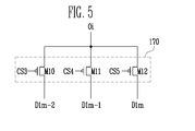
- FIG. 5 is a circuit diagram showing a demultiplexer shown in FIG. 2 .
- FIG. 6 is a circuit diagram showing a connection structure of a demultiplexer, a common circuit unit, and pixels.
- FIG. 7 is a waveform diagram for showing driving methods of a demultiplexer, a common circuit unit, and pixels shown in FIG. 6 .
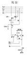
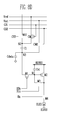
- FIGS. 8A , 8B , 8C , 8D , and 8E are circuit diagrams for showing a driving process according to the waveform diagram of FIG. 7 .
- first element when a first element is described as being connected or coupled to a second element, the first element may be directly coupled to the second element or indirectly coupled to the second element via a third element. Further, some of the elements that are not essential to a complete understanding of the invention are omitted for clarity. Also, like reference numerals refer to like elements throughout.
- FIG. 2 is a block diagram showing an organic light emitting display device according to an embodiment of the present invention.
- a demultiplexer hereinafter, referred to as "DEMUX" 170 is connected to j (j is a natural number of 2 or more) data lines, but it is assumed that j is 3 for the convenience of description.
- the organic light emitting display device includes a display unit 130 that includes pixels 140 positioned at regions where first scan lines S11 to S1 n and second scan lines S21 to S2n cross second data lines D21 to D2m, common circuit units 160, which are connected between first data lines D11 to D1m and the second data lines D21 to D2m and are connected to the DEMUXs 170 through the first data lines D11 to D1m, a scan driver 110 for driving the first scan lines S11 to S1 n, the second scan lines S21 to S2n, and emission control lines E1 to En, a data driver 120 for providing j data signals to each of output lines O1 to Oi, respectively, during a horizontal period, and a timing controller 150 for controlling the scan driver 110 and the data driver 120.
- a display unit 130 that includes pixels 140 positioned at regions where first scan lines S11 to S1 n and second scan lines S21 to S2n cross second data lines D21 to D2m, common circuit units 160, which are connected between first data lines D11 to
- each of the DEMUXs 170 is connected to a corresponding one of the output lines O1 to Oi.
- Each of the output lines O1 to Oi provides j data signals to a connected one of the DEMUXs 170 during a horizontal period.
- the organic light emitting display device includes a switch control unit 180 for controlling the common circuit units 160.
- the scan driver 110 receives a scan driving control signal SCS from the timing controller 150.
- the scan driver 110 that receives the scan driving control signal SCS generates and sequentially provides first scan signals to the first scan lines S11 to S1 n and generates and sequentially provides second scan signals to the second scan lines S21 to S2n.
- the scan driver 110 generates and sequentially provides emission control signals to the emission control lines E1 to En.
- the first scan signals and the second scan signals are set to a voltage (e.g., low voltage) at which transistors included in the pixel 140 may be turned on, and the emission control signals are set to a voltage (e.g., high voltage) at which the transistors included in the pixel 140 may be turned off.
- a second scan signal provided to a k-th (k is a natural number) second scan line S2k is provided earlier than a first scan signal provided to a k-th first scan line S1 k and stops to be provided after the first scan signal stops to be provided.
- the emission control signal provided to the emission control line (E1 to En) is provided to be overlapped with two second scan signals. For example, the emission control signal provided to the k-th emission control line Ek overlaps with the second scan signals provided to a k-th second scan line S2k and a (k+1)-th second scan line S2k+1.
- the data driver 120 receives a data driving control signal DCS from the timing controller 150.
- the data driver 120 that receives the data driving control signal DCS provides j data signals to each of the output lines O1 to Oi in every horizontal period.
- the data driver 120 provides the data signals to the output lines O1 to Oi during a period when the first scan signal is not provided and the second scan signal is provided.
- the timing controller 150 generates the data driving control signal DCS and the scan driving control signal SCS to correspond to externally provided synchronization signals.
- the data driving control signal DCS generated by the timing controller 150 is provided to the data driver 120, and the scan driving control signal SCS is provided to the scan driver 110.
- the timing controller 150 provides externally provided data Data to the data driver 120.
- Each of the DEMUXs 170 is connected between a corresponding one of the output lines O1 to Oi and j first data lines.
- Each of the DEMUXs 170 distributes j data signals supplied from each of the output lines O1 to Oi to j first data lines D11 to D1m in response to control signals CS1, CS2, and CS3 provided from the switch control unit 180.
- the common circuit units 160 are formed between the first data lines D11 to D1m and the second data lines D21 to D2m, respectively.
- the common circuit units 160 receive an initial voltage Vint and a reference voltage Vref supplied from the outside.
- Each of the common circuit units 160 that receives the initial voltage Vint and the reference voltage Vref controls voltage of a first data line to which the common circuit unit 160 is connected in accordance with the control of the switch control unit 180.
- the switch control unit 180 controls turn-on and turn-off of transistors included in the DEMUXs 170 and the common circuit units 160 while providing control signals CS3 to CS5 to the DEMUXs 170 and control signals CS1 to CS2 to the common circuit units 160.
- the switch control unit 180 provides the third control signal CS3 to the fifth control signal CS5 in order to control three transistors included in the DEMUX 170 and provides the first control signal CS1 and the second control signal CS2 in order to control two transistors included in the common circuit unit 160.
- the switch control unit 180 is additionally shown for the convenience of description according to one embodiment, but the present invention is not limited thereto.
- the switch control unit 180 may be included in the timing controller 150.
- the timing controller 150 generates the first control signal CS1 to the fifth control signal CS5 to control driving of the DEMUXs 170 and the common circuit units 160.
- Each of the pixels 140 receives a first power supply ELVDD and a second power supply ELVSS from the outside.
- the pixels 140 that receive the first power supply ELVDD and the second power supply ELVSS generate light having a luminance (e.g., a predetermined luminance) while controlling the amount of current that flows to the second power supply ELVSS from the first power supply ELVDD to correspond to the data signals.
- a luminance e.g., a predetermined luminance
- FIG. 3 is a circuit diagram showing an embodiment of a pixel shown in FIG. 2 .
- a pixel 140 connected to a 2m-th data line D2m and a 1 n-th scan line S1 n is shown.
- the pixel 140 includes an organic light emitting diode OLED and a pixel circuit 142 for supplying current to the OLED.
- An anode electrode of the OLED is connected to the pixel circuit 142 and a cathode electrode of the OLED is connected to the second power supply ELVSS.
- the OLED generates light having a luminance (e.g., a predetermined luminance) to correspond to the amount of current supplied from the pixel circuit 142.
- the pixel circuit 142 receives a voltage (e.g., a predetermined voltage) corresponding to the data signal and supplies a current corresponding to the received voltage to the OLED.
- a voltage e.g., a predetermined voltage
- the pixel circuit 142 includes first to fourth transistors M1 to M4 and a storage capacitor Cst.
- a first electrode of the first transistor M1 is connected to the common circuit unit 160 through the second data line D2m and a second electrode of the first transistor M1 is connected to a gate electrode of the second transistor M2.
- a gate electrode of the first transistor M1 is connected to the second scan line S2n. The first transistor M1 is turned on when the scan signal is provided to the second scan line S2n.
- a first electrode of the second transistor M2 is connected to the first power supply ELVDD, and a second electrode of the second transistor M2 is connected to a first electrode of the fourth transistor M4.
- the gate electrode of the second transistor M2 is connected to the second electrode of the first transistor M1.
- the second transistor M2 supplies a current corresponding to a voltage applied to its own gate electrode to the OLED through the fourth transistor M4.
- a first electrode of the third transistor M3 is connected to the second electrode of the second transistor M2, and the second electrode of the third transistor M3 is connected to the gate electrode of the second transistor M2.
- a gate electrode of the third transistor M3 is connected to the first scan line S1 n.
- the third transistor M3 is turned on when the scan signal is provided to the first scan line S1 n. In this case, the third transistor M3 remains turned off after the first transistor M1 is turned on and turned off before the first transistor M1 is turned off.
- the second transistor M2 is connected in a diode-connected configuration.
- a first electrode of the fourth transistor M4 is connected to the second electrode of the second transistor M2, and the second electrode of the fourth transistor M4 is connected to the anode electrode of the OLED.
- a gate electrode of the fourth transistor M4 is connected to the emission control line En. The fourth transistor M4 is turned off when the emission control signal is provided and turned on when the emission control signal is not provided.
- the storage capacitor Cst is connected between the gate electrode and the first electrode of the second transistor M2.
- the storage capacitor Cst is charged with a voltage (e.g., a predetermined voltage) to correspond to the voltage applied to the gate electrode of the second transistor M2.
- FIG. 4 is a circuit diagram showing an embodiment of a common circuit unit 160 shown in FIG. 2 .
- the common circuit unit 160 is connected to a 1m-th data line D1m.
- the common circuit unit 160 is connected to a plurality of pixels 140 in a unit of a vertical line (e.g., a column of pixels) , but only one pixel 140 is shown in FIG. 4 .
- the common circuit unit 160 includes a first capacitor C1 having a first terminal connected to the first data line D1m and a second terminal connected to the second data line D2m, a first common transistor CM1 connected between the reference voltage Vref and the first terminal of the first capacitor C1, and a second common transistor CM2 connected between the initial voltage Vint and the second terminal of the first capacitor C1.
- the first common transistor CM1 is connected between the reference voltage Vref and the first terminal of the first capacitor C1 and is turned on when the first control signal CS1 is provided. When the first common transistor CM1 is turned on, the voltage of the reference voltage Vref is supplied to the first terminal of the first capacitor C1.
- the second common transistor CM2 is connected between the initial voltage Vint and the second terminal of the first capacitor C1 and is turned on when the second control signal CS2 is provided. When the second common transistor CM2 is turned on, the voltage of the initial voltage Vint is supplied to the second terminal of the second capacitor C2.
- the first capacitor C1 is formed between the first data line D1m and the second data line D2m.
- the first capacitor C1 varies the voltage (i.e., the voltage of the second data line D2m) supplied to the pixel 140 to correspond to the data signal provided to the DEMUX 170.
- FIG. 5 is a circuit diagram showing an embodiment of a DEMUX 170 shown in FIG. 2 .
- a DEMUX 170 is connected to the i-th output line Oi.
- the DEMUX 170 includes a 10-th transistor M10, an 11-th transistor M11, and a 12-th transistor M12.
- the 10-th transistor M10 is connected between the output line Oi and a (1m-2)-th data line D1m-2.
- the 10-th transistor M10 is turned on when the third control signal CS3 is supplied to provide the data signal provided from the output line Oi to the (1m-2)-th data line D1m-2.
- the 11-th transistor M11 is connected between the output line Oi and a (1m-1)-th data line D1m-1.
- the 11-th transistor M11 is turned on when the fourth control signal CS4 is supplied to provide the data signal provided from the output line Oi to the (1m-1)-th data line D1m-1.
- the 12-th transistor M12 is connected between the output line Oi and the 1m-th data line D1m.
- the 12-th transistor M12 is turned on when the fifth control signal CS5 is supplied to provide the data signal provided from the output line Oi to the 1m-th data line D1m.
- the third control signal CS3 to the fifth control signal CS5 are sequentially supplied, and, as a result, the data signals are supplied to the (1m-2)-th data line D1m-2, the (1m-1)-th data line D1m-1, and the first data line D1m while the 10-th transistor M10 to the 12-th transistor M12 are sequentially turned on.
- FIG. 6 is a circuit diagram showing a connection structure of a demultiplexer, a common circuit unit, and pixels.
- the DEMUX 170 connected to the i-th output line Oi, the common circuit units 160, and the pixels 140 are shown according to one embodiment of the present invention.
- the output line Oi is connected to the DEMUX 170, and the DEMUX 170 includes the 10-th transistor M10, the 11-th transistor M11, and the 12-th transistor M12 that are connected to the first data lines D1m-2, D1m-1, and D1m, respectively.
- the common circuit units 160 are positioned between the first data lines D1m-2, D1m-1, and D1m and the second data lines D2m-2, D2m-1, and D2m, respectively.
- the common circuit units 160 control voltages of the second data lines D2m-2, D2m-1, and D2m to correspond to the initial voltage Vint, the reference voltage Vref, and the data signals.
- a data capacitor Cdata represents an equivalent parasitic capacitor.
- the parasitic capacitor formed by the first data line does not substantially influence driving.
- the pixel 140 connected to a second terminal of the first capacitor C1 are separated from each other in a vertical direction by a distance (e.g., a predetermined distance)
- a parasitic capacitor of the second data line influences driving.
- the parasitic capacitor of the second data line that influences driving is shown as the data capacitor Cdata in FIG. 6 .
- FIG. 7 is a waveform diagram for showing driving methods of a demultiplexer, a common circuit unit, and pixels shown in FIG. 6 .
- a first horizontal period 1 H is divided into a first period t1 to a fifth period t5.
- the first control signal CS1 and the second control signal CS2 are provided during the first period t1.
- the first control signal CS1 is provided during the first period t1 to the fourth period t4
- the second control signal CS2 is provided during the first period t1.
- the first common transistor CM1 When the first control signal CS1 is provided, the first common transistor CM1 is turned on as shown in FIG. 8A .
- FIGS. 8A to 8E when a transistor is turned off, only its reference numeral is shown in the drawing without its circuit symbol. However, it should be understood that the transistor is not physically removed from the circuit shown in FIGS. 8A to 8E .
- the first common transistor CM1 When the first common transistor CM1 is turned on, the voltage of the reference voltage Vref is supplied to a second node N2 (i.e., the first terminal of the first capacitor C1).
- the voltage of the reference voltage Vref is set to a voltage lower than the voltage of a black data signal Vdata(black). The detailed description thereof will be described below.
- the second common transistor CM2 When the second control signal CS2 is provided, the second common transistor CM2 is turned on. When the second common transistor CM2 is turned on, the voltage of the initial voltage Vint is supplied to a third node N3 (i.e., the second terminal of the first capacitor C1).
- the voltage of the initial voltage Vint is set to a voltage sufficiently lower than a voltage obtained by subtracting an absolute value of the threshold voltage of the second transistor M2 from the voltage of the first power supply ELVDD.
- the voltage of the first node N1 when the initial voltage Vint is electrically connected to the first node N3 and the first node N1, the voltage of the first node N1 is set to the voltage lower than the voltage obtained by subtracting the absolute value of the threshold voltage of the second transistor M2 from the voltage of the first power supply ELVDD.
- the first transistor M1 maintains a turn-off state during the first period t1
- the first node N1 i.e., the gate electrode of the second transistor M2 maintains the voltage charged during a previous frame period.
- the second scan signal is provided to the second scan line S2n during the second period t2.
- the first transistor M1 is turned on as shown in FIG. 8B .
- the first node N1 and the third node N3 are electrically connected to each other.
- the second scan signal is provided during the second period t2 to the fifth period t5.
- the first scan signal is provided to the first scan line S1 n during the third period t3.
- the third transistor M3 is turned on as shown in FIG. 8C .
- the second transistor M2 is connected in the diode-connected configuration.
- the voltages of the first node N1 and the third node N3 are set to the voltage obtained by subtracting the absolute value of the threshold voltage of the second transistor M2 from the voltage of the first power supply ELVDD as shown in Equation 1.
- the first scan signal is provided to the first scan line S1 n. That is, in the embodiment of the present invention, it is possible to secure the reliability of an operation by providing the first scan signal after initializing the voltage of the first node N1 by firstly providing the second scan signal.
- the first scan signal stops to be provided.
- the third transistor M3 is turned off.
- the third control signal CS3, the fourth control signal CS4, and the fifth control signal CS5 are sequentially provided while the first control signal CS1 is not provided.
- the first common transistor CM1 is turned off as shown in FIG. 8E .
- the second node N2 maintains the voltage of the reference voltage Vref irrespective of the turn-off of the third transistor M3.
- the 10-th transistor M10 When the third control signal CS3 is provided, the 10-th transistor M10 is turned on. When the 10-th transistor M10 is turned on, the data signal provided to the output line Oi is provided to the second node N2. In this case, the voltage of the second node N2 is changed to the voltage of the data signal from the voltage of the reference voltage Vref.
- V N ⁇ 1 ELVDD - Vth M ⁇ 2 + C ⁇ 1 + Cdata + Cst / C ⁇ 1 ⁇ Vdata - Vref
- Vdata represents the voltage of the data signal.
- the first power supply ELVDD, the threshold voltage of the second transistor M2, the first capacitor C1, the data capacitor Cdata, and the storage capacitor Cst have respective determined values in design.
- the voltage of the reference voltage Vref is set to a value corresponding to the capacitances of the data capacitor Cdata and the first capacitor C1.
- the voltage value of the reference voltage Vref is experimentally set so as to charge the pixel 140 with the desired voltage irrespective of the capacitances of the data capacitor Cdata and the first capacitor C1.
- the voltage value of the voltage Vdata of the data signal varies depending on a gray-level to be expressed. That is, in Equation 2, only the voltage Vdata of the data signal varies depending on the gray-level, and, as a result, the voltage of the first node N1 is determined by the voltage Vdata of the data signal.
- the 11-th transistor M11 and the 12-th transistor M12 are sequentially turned on to correspond to the fourth control signal CS4 and the fifth control signal CS5, respectively.
- the voltage of the first node N1 of the pixel 140 connected to each of the 11-th transistor M11 and the 12-th transistor M12 is set as shown in Equation 2.
- the second scan signal stops to be provided to the second scan line S2n, such that the first transistor M1 is turned off.
- the storage capacitor Cst is charged with the voltage applied to the first node N1 and maintains the charged voltage during the fifth period t5.
- the emission control signal stops to be provided to the emission control line En during a sixth period t6.
- the fourth transistor M4 is turned on.
- the second transistor M2 and the anode electrode of the OLED are electrically connected to each other.
- the second transistor M2 supplies a current corresponding to the voltage applied to the first node N1 to the OLED to emit light corresponding to a gray-level.
- the voltage of the reference voltage Vref is set to a voltage lower than the voltage of the black data signal Vdata(black).
- the voltage of the first node N1 is set to a voltage higher than the voltage of ELVDD -
- Equation 2 when the voltage of the first node N1 is set, the current supplied to the OLED is determined irrespective of the voltage drop of the first power supply ELVDD and the threshold voltage of the second transistor M2.
- is removed from an equation for determining a current flowing on the OLED, and, as a result, it is possible to display an image having a desired luminance irrespective of the voltage drop of the first power supply ELVDD and the threshold voltage of the second transistor M2.
- each of the pixels 140 includes four transistors M1 to M4 and only one capacitor Cst is formed, thereby improving reliability and reducing manufacturing cost.
Landscapes
- Engineering & Computer Science (AREA)
- Physics & Mathematics (AREA)
- Computer Hardware Design (AREA)
- General Physics & Mathematics (AREA)
- Theoretical Computer Science (AREA)
- Control Of El Displays (AREA)
- Control Of Indicators Other Than Cathode Ray Tubes (AREA)
- Electroluminescent Light Sources (AREA)
Abstract
The common circuit (160) comprises a capacitor (C1) coupling a first data line (D1m) to a second date line (D2m). In a threshold voltage detection period, the drive-TFT (M2) of a pixel is diode-connected (M3) and the common circuit capacitor (C1) stores a voltage corresponding to the threshold voltage of the drive-TFT (M2) to perform threshold voltage compensation in a subsequent writing period.

Description
- This application claims priority to and the benefit of Korean Patent Application No.
10-2009-0082451, filed on September 2, 2009 - An aspect of an embodiment of the present invention relates to an organic light emitting display device and a driving method thereof.
- Various flat panel display devices with reduced weight and volume in comparison to a cathode ray tube have been developed. Examples of the flat panel display devices include a liquid crystal display device, a field emission display device, a plasma display panel, an organic light emitting display device, etc.
- Among the flat panel display devices, the organic light emitting display device displays an image by using organic light emitting diodes that emit light by recombining holes with electrons. The organic light emitting display device has low power consumption while having high response speed.
-
FIG. 1 is a circuit diagram showing a pixel of an organic light emitting display device according the related art. - Referring to
FIG. 1 , apixel 4 includes apixel circuit 2 for controlling an organic light emitting diode (OLED) connected to thepixel circuit 2, a data line Dm, and a scan line Sn. - An anode electrode of the OLED is connected to the
pixel circuit 2, and a cathode electrode of the OLED is connected to a second power supply ELVSS. The OLED generates light having a luminance (e.g., a predetermined luminance) corresponding to the amount of current supplied from thepixel circuit 2. - The
pixel circuit 2 controls the amount of current supplied to the OLED to correspond to a data signal provided from the data line Dm when a scan signal is provided to the scan line Sn. Here, thepixel circuit 2 includes a second transistor M2 connected to a first power supply ELVDD and the OLED, a first transistor M1 connected to the second transistor M2, the data line Dm, and the scan line Sn, and a storage capacitor Cst connected between a gate electrode and a first electrode of the second transistor M2. - A gate electrode of the first transistor M1 is connected to the scan line Sn, and a first electrode of the first transistor M1 is connected to the data line Dm. In addition, a second electrode of the first transistor M1 is connected to one terminal of the storage capacitor Cst. Here, the first electrode is one of a source electrode or a drain electrode, and the second electrode is an electrode other than the first electrode. For example, when the first electrode is the source electrode, the second electrode is a drain electrode. The first transistor M1 connected to the scan line Sn and the data line Dm is turned on and provides the data signal provided from the data line Dm to the storage capacitor Cst when a scan signal is provided from the scan line Sn. Here, the storage capacitor Cst is charged with a voltage corresponding to the data signal.
- The gate electrode of the second transistor M2 is connected to one terminal of the storage capacitor Cst, and the first electrode of the second transistor M2 is connected to the other terminal of the storage capacitor Cst and the first power supply ELVDD. In addition, a second electrode of the second transistor M2 is connected to the anode electrode of the OLED. The second transistor M2 controls the amount of current that flows to the second power supply ELVSS via the OLED from the first power supply ELVDD to correspond to a voltage value stored in the storage capacitor Cst. Here, the OLED generates light corresponding to the amount of current supplied from the second transistor M2.
- The
pixel circuit 2 supplies a current corresponding to the voltage charged in the storage capacitor Cst to the OLED to display an image having a luminance (e.g., a predetermined luminance). However, the above described organic light emitting display device cannot display an image having uniform luminance due to a variation in threshold voltage of the second transistor M2. - In the related art, additional circuits such as a plurality of transistors are included in the
pixel 4 for compensating for the variation of the threshold voltage of the second transistor M2. However, when the plurality of transistors (for example, 6 transistors) are included in thepixel 4 in order to compensate for the variation of the threshold voltage of the second transistor M2, reliability is deteriorated. - Further, in the related art, a voltage value of the first power supply ELVDD varies due to a voltage drop depending on the position of the
pixel 4, and as a result, an image having desired luminance cannot be displayed. - An aspect of an embodiment of the present invention provides an organic light emitting display device that may compensate for a threshold voltage of a driving transistor and a voltage drop of a first voltage supplied to the driving transistor.
- According to an embodiment of the present invention, an organic light emitting display device is driven during a horizontal period comprising first, second, third, fourth, and fifth periods. The organic light emitting display device includes: a scan driver for driving one or more scan lines and emission control lines grouped by horizontal lines of the organic light emitting display device and extending along an horizontal direction; a data driver for sequentially providing j data signals to each of a plurality of output lines of the data driver in every horizontal period; a demultiplexer for transmitting the j data signals to j first data lines, the demultiplexer being coupled to the output lines; a plurality of second data lines extending along a direction perpendicular to the scan lines; a plurality of pixels at crossing regions of the scan lines and second data lines; and a plurality of common circuit units for controlling voltages of the second data lines coupled to the pixels by using a reference voltage, an initial voltage and the data signals, the common circuit units being coupled between the first data lines and the second data lines.
- Preferably, the reference voltage is a voltage that is lower than a voltage of a black data signal for expressing a black gray-level. Preferably, the initial voltage is a voltage that is lower than a voltage obtained by subtracting an absolute value of a threshold voltage of the second transistor from a voltage of the first power supply.
- The organic light emitting display device may comprise a switch control unit for controlling the demultiplexer and the common circuit unit.
- Preferably, the common circuit unit comprises: a first capacitor coupled between one of the first data lines and one of the second data lines; a first common transistor coupled between said one of the first data lines and a voltage source for providing the reference voltage and configured to be turned on in response to a first control signal from the switch control unit; and a second common transistor coupled between said one of the second data lines and a voltage source for providing the initial voltage and configured to be turned on in response to a second control signal from the switch control unit.
- Preferably, each demultiplexer comprises j transistors coupled between one of the output lines and the j first data lines, and the j transistors being configured to be sequentially turned on in response to j control signals provided from the switch control unit. The j control signals may be sequentially provided during the fifth period of the horizontal period.
- Preferably, the switch control unit provides the first control signal and the second control signal in each horizontal period, the second control signal being longer than the first control signal. Preferably, the second control signal is provided during the first period of the horizontal period and the first control signal is provided during the first to fourth periods of the horizontal period. Preferably, the j control signals for controlling the demultiplexer are not overlapped with the first control signal and the second control signal in each horizontal period.
- Each of the horizontal lines may comprise a first scan line of the scan lines, a second scan line of the scan lines, and one of the emission control lines.
- Preferably, the scan driver sequentially provides first scan signals to the first scan lines, sequentially provides second scan signals to the second scan lines and sequentially provides emission control signals to the emission control lines.
- Each of the pixels may comprise an organic light emitting diode having a cathode electrode coupled to a second power supply; a second transistor having a first electrode coupled to a first power supply for controlling an amount of current supplied to the organic light emitting diode; a first transistor coupled between a gate electrode of the second transistor and one of the second data lines and configured to be turned on when the second scan signals are provided to said one of the second scan lines; a third transistor coupled between the gate electrode of the second transistor and a second electrode of the second transistor and configured to be turned on when a first scan signal is provided to one of the first scan lines coupled to a gate electrode of the third transistor; and a fourth transistor coupled between the second transistor and an anode electrode of the organic light emitting diode and configured to be turned off when the emission control signals are provided to said one of the emission control lines.
- Preferably, the scan driver provides the second scan signals during the second to fifth periods of the horizontal period and provides the first scan signals during the third period of the horizontal period. Preferably, each of the emission control signals overlaps with at least two of the second scan signals.
- The data driver may sequentially provide the j data signals during the fifth period of the horizontal period.
According to an embodiment of the present invention, there is provided a driving method of an organic light emitting display device that includes a pixel including a first capacitor coupled between a first data line for receiving a data signal and a second data line coupled to the pixel and a driving transistor for controlling an amount of current flowing to a second power supply from a first power supply through an organic light emitting diode. The method includes: supplying a reference voltage to the first data line and supplying an initial voltage to the second data line; electrically coupling the second data line to a gate electrode of the driving transistor while supplying the reference voltage to the first data line; increasing the voltage of the second data line to a voltage obtained by subtracting an absolute value of a threshold voltage of the driving transistor from a voltage of the first power supply by electrically coupling the driving transistor in a diode-connected configuration while supplying the reference voltage to the first data line; and varying a voltage of the gate electrode of the driving transistor by providing data signals to the first data line.
Preferably, the driving transistor is in a diode-connected configuration during said varying the voltage of the gate electrode of the driving transistor. - According to the above described embodiments of the present invention, an organic light emitting display device can display an image having a desired luminance irrespective of the voltage drop of a first power supply and the threshold voltage of a driving transistor. According to the embodiments of the present invention, it is possible to compensate for the voltage drop of the first power supply and the threshold voltage of the driving transistor by using a relatively simple structure in which four transistors and one capacitor are included in a pixel, thereby improving reliability. Further, the embodiments of the present invention may be applied to an organic light emitting display device using a demultiplexer.
- The accompanying drawings, together with the specification, illustrate exemplary embodiments of the present invention and, together with the description, serve to explain the principles of the present invention.
-
FIG. 1 is a circuit diagram showing a pixel of an organic light emitting display device according to the related art. -
FIG. 2 is a block diagram showing an organic light emitting display device according to an embodiment of the present invention. -
FIG. 3 is a circuit diagram showing an embodiment of a pixel shown inFIG. 2 . -
FIG. 4 is a circuit diagram showing an embodiment of a common circuit unit shown inFIG. 2 . -
FIG. 5 is a circuit diagram showing a demultiplexer shown inFIG. 2 . -
FIG. 6 is a circuit diagram showing a connection structure of a demultiplexer, a common circuit unit, and pixels. -
FIG. 7 is a waveform diagram for showing driving methods of a demultiplexer, a common circuit unit, and pixels shown inFIG. 6 . -
FIGS. 8A ,8B ,8C ,8D ,and 8E are circuit diagrams for showing a driving process according to the waveform diagram ofFIG. 7 . - Hereinafter, certain exemplary embodiments according to the present invention will be described with reference to the accompanying drawings. Here, when a first element is described as being connected or coupled to a second element, the first element may be directly coupled to the second element or indirectly coupled to the second element via a third element. Further, some of the elements that are not essential to a complete understanding of the invention are omitted for clarity. Also, like reference numerals refer to like elements throughout.
- Hereinafter, exemplary embodiments of the present invention will be described in detail with reference to
FIGS. 2 to 8E . -
FIG. 2 is a block diagram showing an organic light emitting display device according to an embodiment of the present invention. InFIG. 2 , a demultiplexer (hereinafter, referred to as "DEMUX") 170 is connected to j (j is a natural number of 2 or more) data lines, but it is assumed that j is 3 for the convenience of description. - Referring to
FIG. 2 , the organic light emitting display device according to one embodiment of the present invention includes adisplay unit 130 that includespixels 140 positioned at regions where first scan lines S11 to S1 n and second scan lines S21 to S2n cross second data lines D21 to D2m,common circuit units 160, which are connected between first data lines D11 to D1m and the second data lines D21 to D2m and are connected to theDEMUXs 170 through the first data lines D11 to D1m, ascan driver 110 for driving the first scan lines S11 to S1 n, the second scan lines S21 to S2n, and emission control lines E1 to En, adata driver 120 for providing j data signals to each of output lines O1 to Oi, respectively, during a horizontal period, and atiming controller 150 for controlling thescan driver 110 and thedata driver 120. - In addition, according to one embodiment of the present invention, each of the
DEMUXs 170 is connected to a corresponding one of the output lines O1 to Oi. Each of the output lines O1 to Oi provides j data signals to a connected one of theDEMUXs 170 during a horizontal period. The organic light emitting display device according to one embodiment of the present invention includes aswitch control unit 180 for controlling thecommon circuit units 160. - The
scan driver 110 receives a scan driving control signal SCS from thetiming controller 150. Thescan driver 110 that receives the scan driving control signal SCS generates and sequentially provides first scan signals to the first scan lines S11 to S1 n and generates and sequentially provides second scan signals to the second scan lines S21 to S2n. In addition, thescan driver 110 generates and sequentially provides emission control signals to the emission control lines E1 to En. - Here, the first scan signals and the second scan signals are set to a voltage (e.g., low voltage) at which transistors included in the
pixel 140 may be turned on, and the emission control signals are set to a voltage (e.g., high voltage) at which the transistors included in thepixel 140 may be turned off. In addition, a second scan signal provided to a k-th (k is a natural number) second scan line S2k is provided earlier than a first scan signal provided to a k-th first scan line S1 k and stops to be provided after the first scan signal stops to be provided. Further, the emission control signal provided to the emission control line (E1 to En) is provided to be overlapped with two second scan signals. For example, the emission control signal provided to the k-th emission control line Ek overlaps with the second scan signals provided to a k-th second scan line S2k and a (k+1)-th second scanline S2k+ 1. - The
data driver 120 receives a data driving control signal DCS from thetiming controller 150. Thedata driver 120 that receives the data driving control signal DCS provides j data signals to each of the output lines O1 to Oi in every horizontal period. Here, thedata driver 120 provides the data signals to the output lines O1 to Oi during a period when the first scan signal is not provided and the second scan signal is provided. - The
timing controller 150 generates the data driving control signal DCS and the scan driving control signal SCS to correspond to externally provided synchronization signals. The data driving control signal DCS generated by thetiming controller 150 is provided to thedata driver 120, and the scan driving control signal SCS is provided to thescan driver 110. In addition, thetiming controller 150 provides externally provided data Data to thedata driver 120. - Each of the
DEMUXs 170 is connected between a corresponding one of the output lines O1 to Oi and j first data lines. Each of theDEMUXs 170 distributes j data signals supplied from each of the output lines O1 to Oi to j first data lines D11 to D1m in response to control signals CS1, CS2, and CS3 provided from theswitch control unit 180. - The
common circuit units 160 are formed between the first data lines D11 to D1m and the second data lines D21 to D2m, respectively. Thecommon circuit units 160 receive an initial voltage Vint and a reference voltage Vref supplied from the outside. Each of thecommon circuit units 160 that receives the initial voltage Vint and the reference voltage Vref controls voltage of a first data line to which thecommon circuit unit 160 is connected in accordance with the control of theswitch control unit 180. - The
switch control unit 180 controls turn-on and turn-off of transistors included in theDEMUXs 170 and thecommon circuit units 160 while providing control signals CS3 to CS5 to theDEMUXs 170 and control signals CS1 to CS2 to thecommon circuit units 160. Here, theswitch control unit 180 provides the third control signal CS3 to the fifth control signal CS5 in order to control three transistors included in theDEMUX 170 and provides the first control signal CS1 and the second control signal CS2 in order to control two transistors included in thecommon circuit unit 160. - In
FIG. 2 , theswitch control unit 180 is additionally shown for the convenience of description according to one embodiment, but the present invention is not limited thereto. As one example, theswitch control unit 180 may be included in thetiming controller 150. In this case, thetiming controller 150 generates the first control signal CS1 to the fifth control signal CS5 to control driving of theDEMUXs 170 and thecommon circuit units 160. - Each of the
pixels 140 receives a first power supply ELVDD and a second power supply ELVSS from the outside. Thepixels 140 that receive the first power supply ELVDD and the second power supply ELVSS generate light having a luminance (e.g., a predetermined luminance) while controlling the amount of current that flows to the second power supply ELVSS from the first power supply ELVDD to correspond to the data signals. -
FIG. 3 is a circuit diagram showing an embodiment of a pixel shown inFIG. 2 . InFIG. 3 , apixel 140 connected to a 2m-th data line D2m and a 1 n-th scan line S1 n is shown. - Referring to
FIG. 3 , thepixel 140 according to one embodiment of the present invention includes an organic light emitting diode OLED and apixel circuit 142 for supplying current to the OLED. - An anode electrode of the OLED is connected to the
pixel circuit 142 and a cathode electrode of the OLED is connected to the second power supply ELVSS. The OLED generates light having a luminance (e.g., a predetermined luminance) to correspond to the amount of current supplied from thepixel circuit 142. - The
pixel circuit 142 receives a voltage (e.g., a predetermined voltage) corresponding to the data signal and supplies a current corresponding to the received voltage to the OLED. Here, thepixel circuit 142 includes first to fourth transistors M1 to M4 and a storage capacitor Cst. - A first electrode of the first transistor M1 is connected to the
common circuit unit 160 through the second data line D2m and a second electrode of the first transistor M1 is connected to a gate electrode of the second transistor M2. In addition, a gate electrode of the first transistor M1 is connected to the second scan line S2n. The first transistor M1 is turned on when the scan signal is provided to the second scan line S2n. - A first electrode of the second transistor M2 is connected to the first power supply ELVDD, and a second electrode of the second transistor M2 is connected to a first electrode of the fourth transistor M4. In addition, the gate electrode of the second transistor M2 is connected to the second electrode of the first transistor M1. The second transistor M2 supplies a current corresponding to a voltage applied to its own gate electrode to the OLED through the fourth transistor M4.
- A first electrode of the third transistor M3 is connected to the second electrode of the second transistor M2, and the second electrode of the third transistor M3 is connected to the gate electrode of the second transistor M2. In addition, a gate electrode of the third transistor M3 is connected to the first scan line S1 n. The third transistor M3 is turned on when the scan signal is provided to the first scan line S1 n.
In this case, the third transistor M3 remains turned off after the first transistor M1 is turned on and turned off before the first transistor M1 is turned off. Here, when the third transistor M3 is turned on, the second transistor M2 is connected in a diode-connected configuration. - A first electrode of the fourth transistor M4 is connected to the second electrode of the second transistor M2, and the second electrode of the fourth transistor M4 is connected to the anode electrode of the OLED. In addition, a gate electrode of the fourth transistor M4 is connected to the emission control line En. The fourth transistor M4 is turned off when the emission control signal is provided and turned on when the emission control signal is not provided.
- The storage capacitor Cst is connected between the gate electrode and the first electrode of the second transistor M2. The storage capacitor Cst is charged with a voltage (e.g., a predetermined voltage) to correspond to the voltage applied to the gate electrode of the second transistor M2.
-
FIG. 4 is a circuit diagram showing an embodiment of acommon circuit unit 160 shown inFIG. 2 . InFIG. 4 , thecommon circuit unit 160 is connected to a 1m-th data line D1m. In addition, thecommon circuit unit 160 is connected to a plurality ofpixels 140 in a unit of a vertical line (e.g., a column of pixels) , but only onepixel 140 is shown inFIG. 4 . - Referring to
FIG. 4 , thecommon circuit unit 160 includes a first capacitor C1 having a first terminal connected to the first data line D1m and a second terminal connected to the second data line D2m, a first common transistor CM1 connected between the reference voltage Vref and the first terminal of the first capacitor C1, and a second common transistor CM2 connected between the initial voltage Vint and the second terminal of the first capacitor C1. - The first common transistor CM1 is connected between the reference voltage Vref and the first terminal of the first capacitor C1 and is turned on when the first control signal CS1 is provided. When the first common transistor CM1 is turned on, the voltage of the reference voltage Vref is supplied to the first terminal of the first capacitor C1.
- The second common transistor CM2 is connected between the initial voltage Vint and the second terminal of the first capacitor C1 and is turned on when the second control signal CS2 is provided. When the second common transistor CM2 is turned on, the voltage of the initial voltage Vint is supplied to the second terminal of the second capacitor C2.
- The first capacitor C1 is formed between the first data line D1m and the second data line D2m. The first capacitor C1 varies the voltage (i.e., the voltage of the second data line D2m) supplied to the
pixel 140 to correspond to the data signal provided to theDEMUX 170. -
FIG. 5 is a circuit diagram showing an embodiment of aDEMUX 170 shown inFIG. 2 . InFIG. 5 , aDEMUX 170 is connected to the i-th output line Oi. - Referring to
FIG. 5 , theDEMUX 170 includes a 10-th transistor M10, an 11-th transistor M11, and a 12-th transistor M12. - The 10-th transistor M10 is connected between the output line Oi and a (1m-2)-th data line D1m-2. The 10-th transistor M10 is turned on when the third control signal CS3 is supplied to provide the data signal provided from the output line Oi to the (1m-2)-th data line D1m-2.
- The 11-th transistor M11 is connected between the output line Oi and a (1m-1)-th data line D1m-1. The 11-th transistor M11 is turned on when the fourth control signal CS4 is supplied to provide the data signal provided from the output line Oi to the (1m-1)-th data line D1m-1.
- The 12-th transistor M12 is connected between the output line Oi and the 1m-th data line D1m. The 12-th transistor M12 is turned on when the fifth control signal CS5 is supplied to provide the data signal provided from the output line Oi to the 1m-th data line D1m.
- Here, the third control signal CS3 to the fifth control signal CS5 are sequentially supplied, and, as a result, the data signals are supplied to the (1m-2)-th data line D1m-2, the (1m-1)-th data line D1m-1, and the first data line D1m while the 10-th transistor M10 to the 12-th transistor M12 are sequentially turned on.
-
FIG. 6 is a circuit diagram showing a connection structure of a demultiplexer, a common circuit unit, and pixels. InFIG. 6 , theDEMUX 170 connected to the i-th output line Oi, thecommon circuit units 160, and thepixels 140 are shown according to one embodiment of the present invention. - Referring to
FIG. 6 , the output line Oi is connected to theDEMUX 170, and theDEMUX 170 includes the 10-th transistor M10, the 11-th transistor M11, and the 12-th transistor M12 that are connected to the first data lines D1m-2, D1m-1, and D1m, respectively. - The
common circuit units 160 are positioned between the first data lines D1m-2, D1m-1, and D1m and the second data lines D2m-2, D2m-1, and D2m, respectively. Thecommon circuit units 160 control voltages of the second data lines D2m-2, D2m-1, and D2m to correspond to the initial voltage Vint, the reference voltage Vref, and the data signals. - In addition, in
FIG. 6 , a data capacitor Cdata represents an equivalent parasitic capacitor. Here, since a first terminal of the first capacitor C1 is positioned adjacent to theDEMUX 170, the parasitic capacitor formed by the first data line does not substantially influence driving. However, since thepixel 140 connected to a second terminal of the first capacitor C1 are separated from each other in a vertical direction by a distance (e.g., a predetermined distance), a parasitic capacitor of the second data line influences driving. As a panel becomes larger, the influence of the parasitic capacitor of the second data line becomes larger. Therefore, in one embodiment of the present invention, the parasitic capacitor of the second data line that influences driving is shown as the data capacitor Cdata inFIG. 6 . -
FIG. 7 is a waveform diagram for showing driving methods of a demultiplexer, a common circuit unit, and pixels shown inFIG. 6 . - Referring to
FIG. 7 , a firsthorizontal period 1 H is divided into a first period t1 to a fifth period t5. - First, during the first period t1, the first control signal CS1 and the second control signal CS2 are provided. Here, the first control signal CS1 is provided during the first period t1 to the fourth period t4, and the second control signal CS2 is provided during the first period t1.
- When the first control signal CS1 is provided, the first common transistor CM1 is turned on as shown in
FIG. 8A . InFIGS. 8A to 8E , when a transistor is turned off, only its reference numeral is shown in the drawing without its circuit symbol. However, it should be understood that the transistor is not physically removed from the circuit shown inFIGS. 8A to 8E . When the first common transistor CM1 is turned on, the voltage of the reference voltage Vref is supplied to a second node N2 (i.e., the first terminal of the first capacitor C1). Here, the voltage of the reference voltage Vref is set to a voltage lower than the voltage of a black data signal Vdata(black). The detailed description thereof will be described below. - When the second control signal CS2 is provided, the second common transistor CM2 is turned on. When the second common transistor CM2 is turned on, the voltage of the initial voltage Vint is supplied to a third node N3 (i.e., the second terminal of the first capacitor C1). Here, the voltage of the initial voltage Vint is set to a voltage sufficiently lower than a voltage obtained by subtracting an absolute value of the threshold voltage of the second transistor M2 from the voltage of the first power supply ELVDD. Here, when the initial voltage Vint is electrically connected to the first node N3 and the first node N1, the voltage of the first node N1 is set to the voltage lower than the voltage obtained by subtracting the absolute value of the threshold voltage of the second transistor M2 from the voltage of the first power supply ELVDD.
- Here, since the first transistor M1 maintains a turn-off state during the first period t1, the first node N1 (i.e., the gate electrode of the second transistor M2) maintains the voltage charged during a previous frame period.
- The second scan signal is provided to the second scan line S2n during the second period t2. When the scan signal is provided to the second scan line S2n, the first transistor M1 is turned on as shown in
FIG. 8B . When the first transistor M1 is turned on, the first node N1 and the third node N3 are electrically connected to each other. Here, the second scan signal is provided during the second period t2 to the fifth period t5. - The first scan signal is provided to the first scan line S1 n during the third period t3. When the first scan signal is provided to the first scan line S1 n, the third transistor M3 is turned on as shown in
FIG. 8C . When the third transistor M3 is turned on, the second transistor M2 is connected in the diode-connected configuration. In this case, the voltages of the first node N1 and the third node N3 are set to the voltage obtained by subtracting the absolute value of the threshold voltage of the second transistor M2 from the voltage of the first power supply ELVDD as shown inEquation 1.
- Here, in one embodiment of the present invention, after the second scan signal is provided to the second scan line S2n, the first scan signal is provided to the first scan line S1 n. That is, in the embodiment of the present invention, it is possible to secure the reliability of an operation by providing the first scan signal after initializing the voltage of the first node N1 by firstly providing the second scan signal.
- During the fourth period t4, the first scan signal stops to be provided. When the first scan signal stops to be provided, the third transistor M3 is turned off.
- During the fifth period t5, the third control signal CS3, the fourth control signal CS4, and the fifth control signal CS5 are sequentially provided while the first control signal CS1 is not provided. When the first control signal CS1 is not provided, the first common transistor CM1 is turned off as shown in
FIG. 8E . Here, since the first control signal CS1 stops to be provided after the first scan signal stops to be provided, the second node N2 maintains the voltage of the reference voltage Vref irrespective of the turn-off of the third transistor M3. - When the third control signal CS3 is provided, the 10-th transistor M10 is turned on. When the 10-th transistor M10 is turned on, the data signal provided to the output line Oi is provided to the second node N2. In this case, the voltage of the second node N2 is changed to the voltage of the data signal from the voltage of the reference voltage Vref.
- When the voltage of the second node N2 is changed to the voltage of the data signal from the voltage of the reference voltage Vref, the voltage of the first node N1 varies as shown in
Equation 2 to correspond to the variation of the voltage of the second node N2 from a voltage of ELVDD - | Vth(M2) |.
- In
Equation 2, Vdata represents the voltage of the data signal. - In
Equation 2, the first power supply ELVDD, the threshold voltage of the second transistor M2, the first capacitor C1, the data capacitor Cdata, and the storage capacitor Cst have respective determined values in design. In addition, the voltage of the reference voltage Vref is set to a value corresponding to the capacitances of the data capacitor Cdata and the first capacitor C1. Here, the voltage value of the reference voltage Vref is experimentally set so as to charge thepixel 140 with the desired voltage irrespective of the capacitances of the data capacitor Cdata and the first capacitor C1. - The voltage value of the voltage Vdata of the data signal varies depending on a gray-level to be expressed. That is, in
Equation 2, only the voltage Vdata of the data signal varies depending on the gray-level, and, as a result, the voltage of the first node N1 is determined by the voltage Vdata of the data signal. - Thereafter, the 11-th transistor M11 and the 12-th transistor M12 are sequentially turned on to correspond to the fourth control signal CS4 and the fifth control signal CS5, respectively. At this time, the voltage of the first node N1 of the
pixel 140 connected to each of the 11-th transistor M11 and the 12-th transistor M12 is set as shown inEquation 2. - After the fifth period t5, the second scan signal stops to be provided to the second scan line S2n, such that the first transistor M1 is turned off. In this case, the storage capacitor Cst is charged with the voltage applied to the first node N1 and maintains the charged voltage during the fifth period t5.
- Thereafter, the emission control signal stops to be provided to the emission control line En during a sixth period t6. When the emission control signal stops to be provided to the emission control line En, the fourth transistor M4 is turned on. When the fourth transistor M4 is turned on, the second transistor M2 and the anode electrode of the OLED are electrically connected to each other. In this case, the second transistor M2 supplies a current corresponding to the voltage applied to the first node N1 to the OLED to emit light corresponding to a gray-level.
- Here, in one embodiment of the present invention, the voltage of the reference voltage Vref is set to a voltage lower than the voltage of the black data signal Vdata(black). When the voltage of the reference voltage Vref is set to the voltage lower than the voltage of the black data signal Vdata(black), the voltage of the first node N1 is set to a voltage higher than the voltage of ELVDD - | Vth(M2) | to express a full black color at the time of expressing a black gray-level.
- In addition, as shown in
Equation 2, when the voltage of the first node N1 is set, the current supplied to the OLED is determined irrespective of the voltage drop of the first power supply ELVDD and the threshold voltage of the second transistor M2. In other words, ELVDD - | Vth(M2) | is removed from an equation for determining a current flowing on the OLED, and, as a result, it is possible to display an image having a desired luminance irrespective of the voltage drop of the first power supply ELVDD and the threshold voltage of the second transistor M2. - Further, in one embodiment of the present invention, a relatively simple structure in which each of the
pixels 140 includes four transistors M1 to M4 and only one capacitor Cst is formed, thereby improving reliability and reducing manufacturing cost. - While the present invention has been described in connection with certain exemplary embodiments, it is to be understood that the invention is not limited to the disclosed embodiments, but, on the contrary, is intended to cover various modifications and equivalent arrangements included within the scope of the appended claims, and equivalents thereof.
Claims (15)
- An organic light emitting display device adapted to be driven during a horizontal period comprising first, second, third, fourth, and fifth periods (t1, t2, t3, t4, t5), the organic light emitting device comprising:a scan driver (110) for driving one or more scan lines (S11, S12, S13, S1 n, S21, S22, S23, S2n) and emission control lines (E1, E2, E3, En) grouped by horizontal lines of the organic light emitting display device;a data driver (120) for sequentially providing j data signals to each of a plurality of output lines (O1, 02, Oi) of the data driver (120) in each horizontal period;at least one demultiplexer (170) for transmitting the j data signals to j first data lines (D11, D12, D13, D14, D15, D16, D1m-2, D1m-1, D1m), the demultiplexer being coupled to the output lines (O1, O2, Oi);a plurality of pixels (140) at crossing regions of the scan lines (S11, S12, S13, S1n, S21, S22, S23, S2n) and second data lines (D21, D22, D23, D24, D25, D26, D2m-2, D2m-1, D2m) extending in a direction crossing the scan lines (S11, S12, S13, S1n, S21, S22, S23, S2n); andat least one common circuit unit (160) for controlling voltages of the second data lines (D21, D22, D23, D24, D25, D26, D2m-2, D2m-1, D2m) coupled to the pixels (140) by using a reference voltage (Vref), an initial voltage (Vint) and the data signals, the common circuit unit (160) being coupled between one of the first data lines (D11, D12, D13, D14, D15, D16, D1m-2, D1m-1, D1m) and a corresponding one of the second data lines (D21, D22, D23, D24, D25, D26, D2m-2, D2m-1, D2m).
- The organic light emitting display device of claim 1, further comprising
a switch control unit (180) for controlling the at least one demultiplexer (170) and the at least one common circuit unit (160). - The organic light emitting display device of claim 2, wherein each of the common circuit units (160) comprises:a first capacitor (C1) coupled between one first data line (D1m) of the first data lines (D11, D12, D13, D14, D15, D16, D1m-2, D1m-1, D1m) and one second data line (D2m) of the second data lines (D21, D22, D23, D24, D25, D26, D2m-2, D2m-1, D2m);a first common transistor (CM1) coupled between said one (D1m) of the first data lines (D11, D12, D13, D14, D15, D16, D1m-2, D1m-1, D1m) and a voltage source providing the reference voltage (Vref) and configured to be turned on in response to a first control signal (CS1) from the switch control unit (180); anda second common transistor (CM2) coupled between said one (D2m) of the second data lines (D21, D22, D23, D24, D25, D26, D2m-2, D2m-1, D2m) and a voltage source providing the initial voltage (Vint) and configured to be turned on in response to a second control signal (CS2) from the switch control unit (180).
- The organic light emitting display device of one of claims 2 and 3, wherein each demultiplexer (170) comprises j transistors (M10, M11, M12) coupled between one of the output lines (Oi) and the j first data lines (D1m-2, D1m-1, D1m), and the j transistors (M10, M11, M12) being configured to be sequentially turned on in response to j control signals (CS3, CS4, CS5) provided from the switch control unit (180).
- The organic light emitting display device of claim 4, wherein the switch control unit (180) is configured to sequentially provide the j control signals (CS3, CS4, CS5) during the fifth period (t5) of the horizontal period, and/or
to concurrently provide the first control signal (CS1) and the second control signal (CS2) in each horizontal period, the second control signal (CS2) being longer than the first control signal (CS1). - The organic light emitting display device of claim 5,
wherein the switch control unit (180) is configured to provide the second control signal (CS2) during the first period (t1) of the horizontal period and to provide the first control signal (CS1) during the first to fourth periods (t1, t2, t3, t4) of the horizontal period, and/or
wherein the switch control unit (180) is configured to provide j control signals (CS3, CS4, CS5) for controlling the at least one demultiplexer (170), the j control signals (CS3, CS4, CS5) being not overlapped with the first control signal (CS1) and the second control signal (CS2) in each horizontal period. - The organic light emitting display device of one of the preceding claims, wherein each of the horizontal lines comprises a first scan line (S11, S12, S13, S1n) of the scan lines (S11, S12, S13, S1n, S21, S22, S23, S2n), a second scan line (S21, S22, S23, S2n) of the scan lines (S11, S12, S13, S1n, S21, S22, S23, S2n), and one of the emission control lines (E1, E2, E3, En).
- The organic light emitting display device of claim 7, wherein the scan driver (110) is configured to sequentially provide first scan signals to the first scan lines (S11, S12, S13, S1n), sequentially provide second scan signals to the second scan lines (S21, S22, S23, S2n), and sequentially provide emission control signals to the emission control lines (E1, E2, E3, En).
- The organic light emitting display device of one of claims 7 and 8, wherein each of the pixels (140) comprises:an organic light emitting diode (OLED) having a cathode electrode coupled to a second power supply (ELVSS);a second transistor (M2) having a first electrode coupled to a first power supply (ELVDD) for controlling an amount of current supplied to the organic light emitting diode (OLED);a first transistor (M1) coupled between a gate electrode of the second transistor (M2) and one second data line (D2m) of the second data lines (D21, D22, D23, D24, D25, D26, D2m-2, D2m-1, D2m) and configured to be turned on when the second scan signals are provided to one second scan line (S2n) of the second scan lines ( S21, S22, S23, S2n) coupled to the gate electrode of the first transistor (M1);a third transistor (M3) coupled between the gate electrode of the second transistor (M2) and a second electrode of the second transistor (M2) and configured to be turned on when first scan signals are provided to one first scan line (S1n) of the first scan lines (S11, S12, S13, S1n) coupled to the gate electrode of the third transistor (M3); anda fourth transistor (M4) coupled between the second transistor (M2) and an anode electrode of the organic light emitting diode (OLED) and configured to be turned off when the emission control signals are provided to one emission control line (En) of the emission control lines (E1, E2, E3, En) coupled to the gate electrode of the fourth transistor (M4).
- The organic light emitting display device of one of claims 8 and 9, wherein the scan driver (110) is configured to provide the second scan signals during the second to fifth periods (t2, t3, t4, t5) of the horizontal period and provide the first scan signals during the third period (t3) of the horizontal period.
- The organic light emitting display device of one of claims 8-10, wherein the scan driver (110) is configured to provide emission control signals overlapping with at least two of the second scan signals.
- The organic light emitting display device of one of the preceding claims, wherein the data driver (120) is configured to sequentially provide the j data signals during the fifth period (t5) of the horizontal period.
- A driving method of an organic light emitting display device that comprises a plurality of pixels (140) arranged in a matrix and a plurality of common circuit units (160), each common circuit unit (160) comprising a first capacitor (C1) coupled between a first data line (D1m) for receiving a data signal and a second data line (D2m) coupled to the pixels (140) arranged along a column, each pixel (140 comprising a driving transistor (M2) for controlling an amount of current flowing to a second power supply (ELVSS) from a first power supply (ELVDD) through an organic light emitting diode (OLED), the method comprising:supplying a reference voltage (Vref) to the first data line (D1m) and supplying an initial voltage (Vint) to the second data line (V2m);electrically coupling the second data line (D2m) to a gate electrode of the driving transistor (M2) while supplying the reference voltage (Vref) to the first data line (D1m);increasing the voltage of the second data line (D2m) to a voltage obtained by subtracting an absolute value of a threshold voltage of the driving transistor (M2) from a voltage of the first power supply (ELVDD) by electrically coupling the driving transistor (M2) in a diode-connected configuration while supplying the reference voltage (Vref) to the first data line (D1m); andvarying a voltage of the gate electrode of the driving transistor (M2) by providing data signals to the first data line (D1m).
- The driving method of an organic light emitting display device of claim 13, wherein the reference voltage (Vref) is lower than a voltage of a black data signal for expressing a black gray-level, and/or
wherein the initial voltage (Vint) is lower than the voltage obtained by subtracting the absolute value of the threshold voltage of the driving transistor (M2) from the voltage of the first power supply (ELVDD). - The driving method of an organic light emitting display device of one of claims 13 and 14, wherein the driving transistor (M2) is in a diode-connected configuration during said varying the voltage of the gate electrode of the driving transistor (M2).
Applications Claiming Priority (1)
| Application Number | Priority Date | Filing Date | Title |
|---|---|---|---|
| KR1020090082451A KR101082283B1 (en) | 2009-09-02 | 2009-09-02 | Organic Light Emitting Display Device and Driving Method Thereof |
Publications (2)
| Publication Number | Publication Date |
|---|---|
| EP2299430A1 true EP2299430A1 (en) | 2011-03-23 |
| EP2299430B1 EP2299430B1 (en) | 2013-04-17 |
Family
ID=42727430
Family Applications (1)
| Application Number | Title | Priority Date | Filing Date |
|---|---|---|---|
| EP10169619.3A Not-in-force EP2299430B1 (en) | 2009-09-02 | 2010-07-15 | Organic light emitting display device and driving method thereof |
Country Status (5)
| Country | Link |
|---|---|
| US (1) | US8723763B2 (en) |
| EP (1) | EP2299430B1 (en) |
| JP (1) | JP5308990B2 (en) |
| KR (1) | KR101082283B1 (en) |
| CN (1) | CN102005178B (en) |
Cited By (1)
| Publication number | Priority date | Publication date | Assignee | Title |
|---|---|---|---|---|
| US11798492B2 (en) | 2018-05-25 | 2023-10-24 | Semiconductor Energy Laboratory Co., Ltd. | Display device and electronic device |
Families Citing this family (82)
| Publication number | Priority date | Publication date | Assignee | Title |
|---|---|---|---|---|
| CA2490858A1 (en) | 2004-12-07 | 2006-06-07 | Ignis Innovation Inc. | Driving method for compensated voltage-programming of amoled displays |
| CN102663977B (en) | 2005-06-08 | 2015-11-18 | 伊格尼斯创新有限公司 | For driving the method and system of light emitting device display |
| US9489891B2 (en) | 2006-01-09 | 2016-11-08 | Ignis Innovation Inc. | Method and system for driving an active matrix display circuit |
| US9269322B2 (en) | 2006-01-09 | 2016-02-23 | Ignis Innovation Inc. | Method and system for driving an active matrix display circuit |
| TW200949807A (en) | 2008-04-18 | 2009-12-01 | Ignis Innovation Inc | System and driving method for light emitting device display |
| CA2637343A1 (en) | 2008-07-29 | 2010-01-29 | Ignis Innovation Inc. | Improving the display source driver |
| US9370075B2 (en) | 2008-12-09 | 2016-06-14 | Ignis Innovation Inc. | System and method for fast compensation programming of pixels in a display |
| CA2696778A1 (en) | 2010-03-17 | 2011-09-17 | Ignis Innovation Inc. | Lifetime, uniformity, parameter extraction methods |
| US9351368B2 (en) | 2013-03-08 | 2016-05-24 | Ignis Innovation Inc. | Pixel circuits for AMOLED displays |
| US20140368491A1 (en) | 2013-03-08 | 2014-12-18 | Ignis Innovation Inc. | Pixel circuits for amoled displays |
| US9886899B2 (en) | 2011-05-17 | 2018-02-06 | Ignis Innovation Inc. | Pixel Circuits for AMOLED displays |
| EP2715711A4 (en) | 2011-05-28 | 2014-12-24 | Ignis Innovation Inc | System and method for fast compensation programming of pixels in a display |
| JP6064313B2 (en) * | 2011-10-18 | 2017-01-25 | セイコーエプソン株式会社 | Electro-optical device, driving method of electro-optical device, and electronic apparatus |
| JP6141590B2 (en) * | 2011-10-18 | 2017-06-07 | セイコーエプソン株式会社 | Electro-optical device and electronic apparatus |
| JP5929087B2 (en) * | 2011-10-19 | 2016-06-01 | セイコーエプソン株式会社 | Electro-optical device and electronic apparatus |
| JP5853614B2 (en) * | 2011-11-10 | 2016-02-09 | セイコーエプソン株式会社 | Electro-optical device and electronic apparatus |
| JP5879944B2 (en) | 2011-11-16 | 2016-03-08 | セイコーエプソン株式会社 | Electro-optical device and electronic apparatus |
| JP5929121B2 (en) * | 2011-11-25 | 2016-06-01 | セイコーエプソン株式会社 | Electro-optical device and electronic apparatus |
| JP5887973B2 (en) * | 2012-02-13 | 2016-03-16 | セイコーエプソン株式会社 | Electro-optical device, driving method of electro-optical device, and electronic apparatus |
| JP5845963B2 (en) * | 2012-02-22 | 2016-01-20 | セイコーエプソン株式会社 | Electro-optical device, driving method of electro-optical device, and electronic apparatus |
| JP5821685B2 (en) * | 2012-02-22 | 2015-11-24 | セイコーエプソン株式会社 | Electro-optical device and electronic apparatus |
| JP6015095B2 (en) | 2012-04-25 | 2016-10-26 | セイコーエプソン株式会社 | Electro-optical device and electronic apparatus |
| JP6111531B2 (en) * | 2012-04-25 | 2017-04-12 | セイコーエプソン株式会社 | Electro-optical device, driving method of electro-optical device, and electronic apparatus |
| US9747834B2 (en) | 2012-05-11 | 2017-08-29 | Ignis Innovation Inc. | Pixel circuits including feedback capacitors and reset capacitors, and display systems therefore |
| KR101964769B1 (en) * | 2012-10-26 | 2019-04-03 | 삼성디스플레이 주식회사 | Pixel, display device comprising the same and driving method thereof |
| KR102035718B1 (en) * | 2012-11-26 | 2019-10-24 | 삼성디스플레이 주식회사 | Organic Light Emitting Display Device and Driving Method Thereof |
| US9336717B2 (en) | 2012-12-11 | 2016-05-10 | Ignis Innovation Inc. | Pixel circuits for AMOLED displays |
| US9786223B2 (en) | 2012-12-11 | 2017-10-10 | Ignis Innovation Inc. | Pixel circuits for AMOLED displays |
| US9721505B2 (en) | 2013-03-08 | 2017-08-01 | Ignis Innovation Inc. | Pixel circuits for AMOLED displays |
| CA2894717A1 (en) | 2015-06-19 | 2016-12-19 | Ignis Innovation Inc. | Optoelectronic device characterization in array with shared sense line |
| JP6131662B2 (en) * | 2013-03-22 | 2017-05-24 | セイコーエプソン株式会社 | Display device and electronic device |
| CN103226931B (en) * | 2013-04-27 | 2015-09-09 | 京东方科技集团股份有限公司 | Image element circuit and organic light emitting display |
| CN104751771B (en) * | 2013-12-25 | 2017-09-29 | 昆山国显光电有限公司 | Image element circuit structure, active matrix organic light-emitting display device and its driving method |
| JP2015152775A (en) * | 2014-02-14 | 2015-08-24 | セイコーエプソン株式会社 | Electro-optical device and electronic apparatus |
| TWI512716B (en) * | 2014-04-23 | 2015-12-11 | Au Optronics Corp | Display panel and driving method thereof |
| CN104123912B (en) | 2014-07-03 | 2016-10-19 | 京东方科技集团股份有限公司 | Image element circuit and driving method, display device |
| JP6535441B2 (en) | 2014-08-06 | 2019-06-26 | セイコーエプソン株式会社 | Electro-optical device, electronic apparatus, and method of driving electro-optical device |
| TWI533277B (en) * | 2014-09-24 | 2016-05-11 | 友達光電股份有限公司 | Pixel circuit with organic lighe emitting diode |
| CA2873476A1 (en) | 2014-12-08 | 2016-06-08 | Ignis Innovation Inc. | Smart-pixel display architecture |
| KR102284430B1 (en) * | 2014-12-15 | 2021-08-04 | 삼성디스플레이 주식회사 | Display apparatus |
| CN105810143B (en) * | 2014-12-29 | 2018-09-28 | 昆山工研院新型平板显示技术中心有限公司 | A kind of data drive circuit and its driving method and organic light emitting display |
| CA2886862A1 (en) | 2015-04-01 | 2016-10-01 | Ignis Innovation Inc. | Adjusting display brightness for avoiding overheating and/or accelerated aging |
| US10373554B2 (en) | 2015-07-24 | 2019-08-06 | Ignis Innovation Inc. | Pixels and reference circuits and timing techniques |
| US10657895B2 (en) | 2015-07-24 | 2020-05-19 | Ignis Innovation Inc. | Pixels and reference circuits and timing techniques |
| CA2898282A1 (en) | 2015-07-24 | 2017-01-24 | Ignis Innovation Inc. | Hybrid calibration of current sources for current biased voltage progra mmed (cbvp) displays |
| JP6052365B2 (en) * | 2015-10-02 | 2016-12-27 | セイコーエプソン株式会社 | Electro-optical device and electronic apparatus |
| CA2908285A1 (en) | 2015-10-14 | 2017-04-14 | Ignis Innovation Inc. | Driver with multiple color pixel structure |
| JP6079859B2 (en) * | 2015-12-07 | 2017-02-15 | セイコーエプソン株式会社 | Electro-optical device and electronic apparatus |
| CN106935200A (en) * | 2015-12-29 | 2017-07-07 | 上海和辉光电有限公司 | Organic light-emitting display device and its driving method |
| CN105609048B (en) | 2016-01-04 | 2018-06-05 | 京东方科技集团股份有限公司 | A kind of pixel compensation circuit and its driving method, display device |
| JP6152902B2 (en) * | 2016-01-27 | 2017-06-28 | セイコーエプソン株式会社 | Electro-optical device and electronic apparatus |
| CN105513535A (en) * | 2016-01-29 | 2016-04-20 | 上海天马有机发光显示技术有限公司 | Pixel driving circuit, driving method thereof and array substrate |
| JP6828247B2 (en) | 2016-02-19 | 2021-02-10 | セイコーエプソン株式会社 | Display devices and electronic devices |
| JP6817789B2 (en) * | 2016-06-10 | 2021-01-20 | ラピスセミコンダクタ株式会社 | Display driver and semiconductor device |
| JP6733361B2 (en) * | 2016-06-28 | 2020-07-29 | セイコーエプソン株式会社 | Display device and electronic equipment |
| JP6747156B2 (en) | 2016-08-05 | 2020-08-26 | 天馬微電子有限公司 | Display device |
| JP6773277B2 (en) | 2016-08-05 | 2020-10-21 | 天馬微電子有限公司 | Display device |
| JP6626802B2 (en) * | 2016-09-07 | 2019-12-25 | セイコーエプソン株式会社 | Electro-optical devices and electronic equipment |
| JP6581951B2 (en) * | 2016-09-07 | 2019-09-25 | セイコーエプソン株式会社 | Driving method of electro-optical device |
| JP6213644B2 (en) * | 2016-09-15 | 2017-10-18 | セイコーエプソン株式会社 | Electro-optical device and electronic apparatus |
| JP6520981B2 (en) * | 2017-04-19 | 2019-05-29 | セイコーエプソン株式会社 | Display device and electronic device |
| KR102369624B1 (en) * | 2017-06-30 | 2022-03-03 | 엘지디스플레이 주식회사 | Display panel and electroluminescence display using the same |
| JP6376258B2 (en) * | 2017-09-04 | 2018-08-22 | セイコーエプソン株式会社 | Electro-optical device and electronic apparatus |
| CN107833559B (en) * | 2017-12-08 | 2023-11-28 | 合肥京东方光电科技有限公司 | Pixel driving circuit, organic light-emitting display panel and pixel driving method |
| JP6673388B2 (en) * | 2018-03-09 | 2020-03-25 | セイコーエプソン株式会社 | Driving method of electro-optical device |
| CN110033731B (en) * | 2018-04-18 | 2020-09-25 | 友达光电股份有限公司 | Composite drive display panel |
| KR102485164B1 (en) * | 2018-05-03 | 2023-01-09 | 삼성디스플레이 주식회사 | Driving voltage setting device, method of setting driving voltage for display device, and display device |
| CN108806612B (en) * | 2018-06-13 | 2020-01-10 | 京东方科技集团股份有限公司 | Pixel circuit, driving method thereof and display device |
| JP6673406B2 (en) * | 2018-07-23 | 2020-03-25 | セイコーエプソン株式会社 | Electro-optical devices and electronic equipment |
| CN108986747B (en) * | 2018-07-25 | 2020-07-28 | 京东方科技集团股份有限公司 | Array substrate, organic electroluminescent display panel and display device |
| CN110520922B (en) * | 2018-09-20 | 2021-08-24 | 京东方科技集团股份有限公司 | Display driving circuit, method, and display device |
| JP2019008325A (en) * | 2018-10-03 | 2019-01-17 | セイコーエプソン株式会社 | Electro-optical device and electronic apparatus |
| JP6852749B2 (en) * | 2019-04-25 | 2021-03-31 | セイコーエプソン株式会社 | Display devices and electronic devices |
| CN110648630B (en) * | 2019-09-26 | 2021-02-05 | 京东方科技集团股份有限公司 | Pixel driving circuit, pixel driving method, display panel and display device |
| KR102765391B1 (en) * | 2019-10-18 | 2025-02-12 | 삼성디스플레이 주식회사 | Display panel of an organic light emitting diode display device and organic light emitting diode display device |
| US11763748B2 (en) * | 2019-10-21 | 2023-09-19 | Hewlett-Packard Development Company, L.P. | Pixel-addressable display having curvable area |
| KR102601611B1 (en) * | 2019-12-20 | 2023-11-13 | 엘지디스플레이 주식회사 | Data switching device and display device using the same |
| CN111369941B (en) * | 2020-03-19 | 2021-04-27 | 武汉华星光电半导体显示技术有限公司 | Pixel circuit and display panel |
| CN113160761B (en) * | 2021-04-20 | 2023-10-03 | 惠州市华星光电技术有限公司 | Driving method, driving circuit and display device |
| KR102883434B1 (en) * | 2021-08-10 | 2025-11-07 | 엘지디스플레이 주식회사 | Light Emitting Display Device and Driving Method of the same |
| KR20240062175A (en) * | 2022-10-27 | 2024-05-09 | 삼성디스플레이 주식회사 | Display panel |
| CN117198212B (en) * | 2023-11-07 | 2024-04-12 | 惠科股份有限公司 | Display panel |
Citations (2)
| Publication number | Priority date | Publication date | Assignee | Title |
|---|---|---|---|---|
| EP1755104A2 (en) * | 2005-08-16 | 2007-02-21 | Samsung SDI Co., Ltd. | Organic light emitting display (OLED) |
| EP2093748A1 (en) * | 2007-03-08 | 2009-08-26 | Sharp Kabushiki Kaisha | Display device and its driving method |
Family Cites Families (13)
| Publication number | Priority date | Publication date | Assignee | Title |
|---|---|---|---|---|
| KR100649243B1 (en) | 2002-03-21 | 2006-11-24 | 삼성에스디아이 주식회사 | Organic electroluminescent display and driving method thereof |
| JP4378087B2 (en) | 2003-02-19 | 2009-12-02 | 奇美電子股▲ふん▼有限公司 | Image display device |
| JP5078223B2 (en) | 2003-09-30 | 2012-11-21 | 三洋電機株式会社 | Organic EL pixel circuit |
| JP2005352411A (en) * | 2004-06-14 | 2005-12-22 | Sharp Corp | DRIVE CIRCUIT FOR CURRENT-DRIVEN DISPLAY ELEMENT AND DISPLAY DEVICE HAVING THE SAME |
| KR100602361B1 (en) * | 2004-09-22 | 2006-07-19 | 삼성에스디아이 주식회사 | Demultiplexer, light emitting display device using same and driving method thereof |
| KR100624137B1 (en) * | 2005-08-22 | 2006-09-13 | 삼성에스디아이 주식회사 | Pixel circuit of organic electroluminescent display and driving method thereof |
| KR100732842B1 (en) | 2005-11-09 | 2007-06-27 | 삼성에스디아이 주식회사 | Light emitting display |
| JP5240542B2 (en) * | 2006-09-25 | 2013-07-17 | カシオ計算機株式会社 | Display driving device and driving method thereof, and display device and driving method thereof |
| KR100833760B1 (en) * | 2007-01-16 | 2008-05-29 | 삼성에스디아이 주식회사 | Organic electroluminescent display |
| KR100897171B1 (en) | 2007-07-27 | 2009-05-14 | 삼성모바일디스플레이주식회사 | Organic light emitting display |
| KR101407302B1 (en) * | 2007-12-27 | 2014-06-13 | 엘지디스플레이 주식회사 | Light emitting display and driving method thereof |
| JP2009180765A (en) * | 2008-01-29 | 2009-08-13 | Casio Comput Co Ltd | Display driving device, display device and driving method thereof |
| KR100924143B1 (en) * | 2008-04-02 | 2009-10-28 | 삼성모바일디스플레이주식회사 | Flat Panel Display and Driving Method |
-
2009
- 2009-09-02 KR KR1020090082451A patent/KR101082283B1/en not_active Expired - Fee Related
- 2009-10-29 JP JP2009249367A patent/JP5308990B2/en not_active Expired - Fee Related
-
2010
- 2010-05-21 US US12/785,296 patent/US8723763B2/en active Active
- 2010-07-06 CN CN201010224792.2A patent/CN102005178B/en not_active Expired - Fee Related
- 2010-07-15 EP EP10169619.3A patent/EP2299430B1/en not_active Not-in-force
Patent Citations (2)
| Publication number | Priority date | Publication date | Assignee | Title |
|---|---|---|---|---|
| EP1755104A2 (en) * | 2005-08-16 | 2007-02-21 | Samsung SDI Co., Ltd. | Organic light emitting display (OLED) |
| EP2093748A1 (en) * | 2007-03-08 | 2009-08-26 | Sharp Kabushiki Kaisha | Display device and its driving method |
Cited By (1)
| Publication number | Priority date | Publication date | Assignee | Title |
|---|---|---|---|---|
| US11798492B2 (en) | 2018-05-25 | 2023-10-24 | Semiconductor Energy Laboratory Co., Ltd. | Display device and electronic device |
Also Published As
| Publication number | Publication date |
|---|---|
| US20110050741A1 (en) | 2011-03-03 |
| JP5308990B2 (en) | 2013-10-09 |
| CN102005178A (en) | 2011-04-06 |
| EP2299430B1 (en) | 2013-04-17 |
| KR20110024452A (en) | 2011-03-09 |
| CN102005178B (en) | 2014-01-01 |
| KR101082283B1 (en) | 2011-11-09 |
| US8723763B2 (en) | 2014-05-13 |
| JP2011053635A (en) | 2011-03-17 |
Similar Documents
| Publication | Publication Date | Title |
|---|---|---|
| EP2299430A1 (en) | Organic light emitting display device and driving method thereof | |
| US8654041B2 (en) | Organic light emitting display device having more uniform luminance and method of driving the same | |
| US8907870B2 (en) | Pixel and organic light emitting display device using the pixel | |
| EP2261884B1 (en) | Pixel of an OLED display and the corresponding display | |
| CN101609840B (en) | Pixel and organic light emitting display device using the same | |
| EP2136352B1 (en) | Pixel and organic light emitting display device using the same with compensation of the degradation of the organic light emitting element | |
| US8570249B2 (en) | Pixel coupled to three horizontal lines and organic light emitting display device using the same | |
| US8638279B2 (en) | Pixel and organic light emitting display device using the same | |
| US8378933B2 (en) | Pixel and organic light emitting display device using the same | |
| KR101142729B1 (en) | Pixel and Organic Light Emitting Display Device Using the same | |
| EP2736036A2 (en) | Organic light emitting diode display device and method of driving the same | |
| US8674906B2 (en) | Organic light emitting display device | |
| US8242983B2 (en) | Pixel and organic light emitting display device using the same | |
| US20100128014A1 (en) | Pixel and organic light emitting display device using the same | |
| KR20090102449A (en) | Pixel and organic light emitting display using the same | |
| US20110084959A1 (en) | Pixel and organic light emitting display using the same | |
| KR20100116807A (en) | Organic light emitting display device |
Legal Events
| Date | Code | Title | Description |
|---|---|---|---|
| PUAI | Public reference made under article 153(3) epc to a published international application that has entered the european phase |
Free format text: ORIGINAL CODE: 0009012 |
|
| 17P | Request for examination filed |
Effective date: 20100715 |
|
| AK | Designated contracting states |
Kind code of ref document: A1 Designated state(s): AL AT BE BG CH CY CZ DE DK EE ES FI FR GB GR HR HU IE IS IT LI LT LU LV MC MK MT NL NO PL PT RO SE SI SK SM TR |
|
| AX | Request for extension of the european patent |
Extension state: BA ME RS |
|
| 17Q | First examination report despatched |
Effective date: 20110804 |
|
| RAP1 | Party data changed (applicant data changed or rights of an application transferred) |
Owner name: SAMSUNG MOBILE DISPLAY CO., LTD. |
|
| RAP1 | Party data changed (applicant data changed or rights of an application transferred) |
Owner name: SAMSUNG DISPLAY CO., LTD. |
|
| GRAP | Despatch of communication of intention to grant a patent |
Free format text: ORIGINAL CODE: EPIDOSNIGR1 |
|
| GRAS | Grant fee paid |
Free format text: ORIGINAL CODE: EPIDOSNIGR3 |
|
| GRAA | (expected) grant |
Free format text: ORIGINAL CODE: 0009210 |
|
| AK | Designated contracting states |
Kind code of ref document: B1 Designated state(s): AL AT BE BG CH CY CZ DE DK EE ES FI FR GB GR HR HU IE IS IT LI LT LU LV MC MK MT NL NO PL PT RO SE SI SK SM TR |
|
| REG | Reference to a national code |
Ref country code: GB Ref legal event code: FG4D |
|
| REG | Reference to a national code |
Ref country code: CH Ref legal event code: EP |
|
| REG | Reference to a national code |
Ref country code: IE Ref legal event code: FG4D |
|
| REG | Reference to a national code |
Ref country code: AT Ref legal event code: REF Ref document number: 607736 Country of ref document: AT Kind code of ref document: T Effective date: 20130515 |
|
| REG | Reference to a national code |
Ref country code: DE Ref legal event code: R096 Ref document number: 602010006184 Country of ref document: DE Effective date: 20130613 |
|
| REG | Reference to a national code |
Ref country code: AT Ref legal event code: MK05 Ref document number: 607736 Country of ref document: AT Kind code of ref document: T Effective date: 20130417 |
|
| REG | Reference to a national code |
Ref country code: LT Ref legal event code: MG4D |
|
| REG | Reference to a national code |
Ref country code: NL Ref legal event code: VDEP Effective date: 20130417 |
|
| PG25 | Lapsed in a contracting state [announced via postgrant information from national office to epo] |
Ref country code: PT Free format text: LAPSE BECAUSE OF FAILURE TO SUBMIT A TRANSLATION OF THE DESCRIPTION OR TO PAY THE FEE WITHIN THE PRESCRIBED TIME-LIMIT Effective date: 20130819 Ref country code: NO Free format text: LAPSE BECAUSE OF FAILURE TO SUBMIT A TRANSLATION OF THE DESCRIPTION OR TO PAY THE FEE WITHIN THE PRESCRIBED TIME-LIMIT Effective date: 20130717 Ref country code: FI Free format text: LAPSE BECAUSE OF FAILURE TO SUBMIT A TRANSLATION OF THE DESCRIPTION OR TO PAY THE FEE WITHIN THE PRESCRIBED TIME-LIMIT Effective date: 20130417 Ref country code: SI Free format text: LAPSE BECAUSE OF FAILURE TO SUBMIT A TRANSLATION OF THE DESCRIPTION OR TO PAY THE FEE WITHIN THE PRESCRIBED TIME-LIMIT Effective date: 20130417 Ref country code: SE Free format text: LAPSE BECAUSE OF FAILURE TO SUBMIT A TRANSLATION OF THE DESCRIPTION OR TO PAY THE FEE WITHIN THE PRESCRIBED TIME-LIMIT Effective date: 20130417 Ref country code: ES Free format text: LAPSE BECAUSE OF FAILURE TO SUBMIT A TRANSLATION OF THE DESCRIPTION OR TO PAY THE FEE WITHIN THE PRESCRIBED TIME-LIMIT Effective date: 20130728 Ref country code: BE Free format text: LAPSE BECAUSE OF FAILURE TO SUBMIT A TRANSLATION OF THE DESCRIPTION OR TO PAY THE FEE WITHIN THE PRESCRIBED TIME-LIMIT Effective date: 20130417 Ref country code: GR Free format text: LAPSE BECAUSE OF FAILURE TO SUBMIT A TRANSLATION OF THE DESCRIPTION OR TO PAY THE FEE WITHIN THE PRESCRIBED TIME-LIMIT Effective date: 20130718 Ref country code: IS Free format text: LAPSE BECAUSE OF FAILURE TO SUBMIT A TRANSLATION OF THE DESCRIPTION OR TO PAY THE FEE WITHIN THE PRESCRIBED TIME-LIMIT Effective date: 20130817 Ref country code: AT Free format text: LAPSE BECAUSE OF FAILURE TO SUBMIT A TRANSLATION OF THE DESCRIPTION OR TO PAY THE FEE WITHIN THE PRESCRIBED TIME-LIMIT Effective date: 20130417 Ref country code: LT Free format text: LAPSE BECAUSE OF FAILURE TO SUBMIT A TRANSLATION OF THE DESCRIPTION OR TO PAY THE FEE WITHIN THE PRESCRIBED TIME-LIMIT Effective date: 20130417 |
|
| PG25 | Lapsed in a contracting state [announced via postgrant information from national office to epo] |
Ref country code: LV Free format text: LAPSE BECAUSE OF FAILURE TO SUBMIT A TRANSLATION OF THE DESCRIPTION OR TO PAY THE FEE WITHIN THE PRESCRIBED TIME-LIMIT Effective date: 20130417 Ref country code: BG Free format text: LAPSE BECAUSE OF FAILURE TO SUBMIT A TRANSLATION OF THE DESCRIPTION OR TO PAY THE FEE WITHIN THE PRESCRIBED TIME-LIMIT Effective date: 20130717 Ref country code: HR Free format text: LAPSE BECAUSE OF FAILURE TO SUBMIT A TRANSLATION OF THE DESCRIPTION OR TO PAY THE FEE WITHIN THE PRESCRIBED TIME-LIMIT Effective date: 20130417 Ref country code: PL Free format text: LAPSE BECAUSE OF FAILURE TO SUBMIT A TRANSLATION OF THE DESCRIPTION OR TO PAY THE FEE WITHIN THE PRESCRIBED TIME-LIMIT Effective date: 20130417 Ref country code: CY Free format text: LAPSE BECAUSE OF FAILURE TO SUBMIT A TRANSLATION OF THE DESCRIPTION OR TO PAY THE FEE WITHIN THE PRESCRIBED TIME-LIMIT Effective date: 20130417 |
|
| PG25 | Lapsed in a contracting state [announced via postgrant information from national office to epo] |
Ref country code: SK Free format text: LAPSE BECAUSE OF FAILURE TO SUBMIT A TRANSLATION OF THE DESCRIPTION OR TO PAY THE FEE WITHIN THE PRESCRIBED TIME-LIMIT Effective date: 20130417 Ref country code: DK Free format text: LAPSE BECAUSE OF FAILURE TO SUBMIT A TRANSLATION OF THE DESCRIPTION OR TO PAY THE FEE WITHIN THE PRESCRIBED TIME-LIMIT Effective date: 20130417 Ref country code: EE Free format text: LAPSE BECAUSE OF FAILURE TO SUBMIT A TRANSLATION OF THE DESCRIPTION OR TO PAY THE FEE WITHIN THE PRESCRIBED TIME-LIMIT Effective date: 20130417 Ref country code: CZ Free format text: LAPSE BECAUSE OF FAILURE TO SUBMIT A TRANSLATION OF THE DESCRIPTION OR TO PAY THE FEE WITHIN THE PRESCRIBED TIME-LIMIT Effective date: 20130417 |
|
| PLBE | No opposition filed within time limit |
Free format text: ORIGINAL CODE: 0009261 |
|
| STAA | Information on the status of an ep patent application or granted ep patent |
Free format text: STATUS: NO OPPOSITION FILED WITHIN TIME LIMIT |
|
| PG25 | Lapsed in a contracting state [announced via postgrant information from national office to epo] |
Ref country code: MC Free format text: LAPSE BECAUSE OF FAILURE TO SUBMIT A TRANSLATION OF THE DESCRIPTION OR TO PAY THE FEE WITHIN THE PRESCRIBED TIME-LIMIT Effective date: 20130417 Ref country code: NL Free format text: LAPSE BECAUSE OF FAILURE TO SUBMIT A TRANSLATION OF THE DESCRIPTION OR TO PAY THE FEE WITHIN THE PRESCRIBED TIME-LIMIT Effective date: 20130417 Ref country code: IT Free format text: LAPSE BECAUSE OF FAILURE TO SUBMIT A TRANSLATION OF THE DESCRIPTION OR TO PAY THE FEE WITHIN THE PRESCRIBED TIME-LIMIT Effective date: 20130417 Ref country code: RO Free format text: LAPSE BECAUSE OF FAILURE TO SUBMIT A TRANSLATION OF THE DESCRIPTION OR TO PAY THE FEE WITHIN THE PRESCRIBED TIME-LIMIT Effective date: 20130417 |
|
| 26N | No opposition filed |
Effective date: 20140120 |
|
| REG | Reference to a national code |
Ref country code: IE Ref legal event code: MM4A |
|
| REG | Reference to a national code |
Ref country code: DE Ref legal event code: R097 Ref document number: 602010006184 Country of ref document: DE Effective date: 20140120 |
|
| PG25 | Lapsed in a contracting state [announced via postgrant information from national office to epo] |
Ref country code: IE Free format text: LAPSE BECAUSE OF NON-PAYMENT OF DUE FEES Effective date: 20130715 |
|
| REG | Reference to a national code |
Ref country code: CH Ref legal event code: PL |
|
| PG25 | Lapsed in a contracting state [announced via postgrant information from national office to epo] |
Ref country code: LI Free format text: LAPSE BECAUSE OF NON-PAYMENT OF DUE FEES Effective date: 20140731 Ref country code: CH Free format text: LAPSE BECAUSE OF NON-PAYMENT OF DUE FEES Effective date: 20140731 |
|
| PG25 | Lapsed in a contracting state [announced via postgrant information from national office to epo] |
Ref country code: SM Free format text: LAPSE BECAUSE OF FAILURE TO SUBMIT A TRANSLATION OF THE DESCRIPTION OR TO PAY THE FEE WITHIN THE PRESCRIBED TIME-LIMIT Effective date: 20130417 |
|
| PG25 | Lapsed in a contracting state [announced via postgrant information from national office to epo] |
Ref country code: MT Free format text: LAPSE BECAUSE OF FAILURE TO SUBMIT A TRANSLATION OF THE DESCRIPTION OR TO PAY THE FEE WITHIN THE PRESCRIBED TIME-LIMIT Effective date: 20130417 Ref country code: TR Free format text: LAPSE BECAUSE OF FAILURE TO SUBMIT A TRANSLATION OF THE DESCRIPTION OR TO PAY THE FEE WITHIN THE PRESCRIBED TIME-LIMIT Effective date: 20130417 |
|
| PG25 | Lapsed in a contracting state [announced via postgrant information from national office to epo] |
Ref country code: MK Free format text: LAPSE BECAUSE OF FAILURE TO SUBMIT A TRANSLATION OF THE DESCRIPTION OR TO PAY THE FEE WITHIN THE PRESCRIBED TIME-LIMIT Effective date: 20130417 Ref country code: HU Free format text: LAPSE BECAUSE OF FAILURE TO SUBMIT A TRANSLATION OF THE DESCRIPTION OR TO PAY THE FEE WITHIN THE PRESCRIBED TIME-LIMIT; INVALID AB INITIO Effective date: 20100715 Ref country code: LU Free format text: LAPSE BECAUSE OF NON-PAYMENT OF DUE FEES Effective date: 20130715 |
|
| REG | Reference to a national code |
Ref country code: FR Ref legal event code: PLFP Year of fee payment: 7 |
|
| REG | Reference to a national code |
Ref country code: FR Ref legal event code: PLFP Year of fee payment: 8 |
|
| REG | Reference to a national code |
Ref country code: FR Ref legal event code: PLFP Year of fee payment: 9 |
|
| PG25 | Lapsed in a contracting state [announced via postgrant information from national office to epo] |
Ref country code: AL Free format text: LAPSE BECAUSE OF FAILURE TO SUBMIT A TRANSLATION OF THE DESCRIPTION OR TO PAY THE FEE WITHIN THE PRESCRIBED TIME-LIMIT Effective date: 20130417 |
|
| PGFP | Annual fee paid to national office [announced via postgrant information from national office to epo] |
Ref country code: FR Payment date: 20190624 Year of fee payment: 10 |
|
| PGFP | Annual fee paid to national office [announced via postgrant information from national office to epo] |
Ref country code: DE Payment date: 20190620 Year of fee payment: 10 Ref country code: GB Payment date: 20190621 Year of fee payment: 10 |
|
| REG | Reference to a national code |
Ref country code: DE Ref legal event code: R119 Ref document number: 602010006184 Country of ref document: DE |
|
| GBPC | Gb: european patent ceased through non-payment of renewal fee |
Effective date: 20200715 |
|
| PG25 | Lapsed in a contracting state [announced via postgrant information from national office to epo] |
Ref country code: GB Free format text: LAPSE BECAUSE OF NON-PAYMENT OF DUE FEES Effective date: 20200715 Ref country code: FR Free format text: LAPSE BECAUSE OF NON-PAYMENT OF DUE FEES Effective date: 20200731 |
|
| PG25 | Lapsed in a contracting state [announced via postgrant information from national office to epo] |
Ref country code: DE Free format text: LAPSE BECAUSE OF NON-PAYMENT OF DUE FEES Effective date: 20210202 |