EP2297025B1 - Mems devices - Google Patents
Mems devices Download PDFInfo
- Publication number
- EP2297025B1 EP2297025B1 EP09754246.8A EP09754246A EP2297025B1 EP 2297025 B1 EP2297025 B1 EP 2297025B1 EP 09754246 A EP09754246 A EP 09754246A EP 2297025 B1 EP2297025 B1 EP 2297025B1
- Authority
- EP
- European Patent Office
- Prior art keywords
- layer
- silicon
- mems device
- anneal
- forming
- Prior art date
- Legal status (The legal status is an assumption and is not a legal conclusion. Google has not performed a legal analysis and makes no representation as to the accuracy of the status listed.)
- Not-in-force
Links
Images


Classifications
-
- B—PERFORMING OPERATIONS; TRANSPORTING
- B81—MICROSTRUCTURAL TECHNOLOGY
- B81C—PROCESSES OR APPARATUS SPECIALLY ADAPTED FOR THE MANUFACTURE OR TREATMENT OF MICROSTRUCTURAL DEVICES OR SYSTEMS
- B81C1/00—Manufacture or treatment of devices or systems in or on a substrate
- B81C1/00015—Manufacture or treatment of devices or systems in or on a substrate for manufacturing microsystems
- B81C1/00261—Processes for packaging MEMS devices
- B81C1/00277—Processes for packaging MEMS devices for maintaining a controlled atmosphere inside of the cavity containing the MEMS
- B81C1/00293—Processes for packaging MEMS devices for maintaining a controlled atmosphere inside of the cavity containing the MEMS maintaining a controlled atmosphere with processes not provided for in B81C1/00285
-
- B—PERFORMING OPERATIONS; TRANSPORTING
- B81—MICROSTRUCTURAL TECHNOLOGY
- B81C—PROCESSES OR APPARATUS SPECIALLY ADAPTED FOR THE MANUFACTURE OR TREATMENT OF MICROSTRUCTURAL DEVICES OR SYSTEMS
- B81C2203/00—Forming microstructural systems
- B81C2203/01—Packaging MEMS
- B81C2203/0145—Hermetically sealing an opening in the lid
Definitions
- This invention relates to MEMS devices, and in particular to the formation of packaged devices.
- MEMS technologies are increasingly being used in integrated circuits.
- numerous product concepts have not been implemented in practice as a result of difficulties providing suitable and cost effective packaging.
- a capping wafer typically comprises a pre-fabricated cavity formed of glass or silicon.
- Anodic of frit glass bonding is then used, because of the back-end compatible process temperatures (400°C) in preference to fusion bonding at much higher temperatures (1000°C).
- a vacuum inside the cavity can be achieved if the bonding is performed in a vacuum chamber. This approach requires wafer bonding and flip-chip alignment equipment.
- An integrated wafer-level solution involves fabricating caps using standard surface micro machining techniques. This approach consumes less area and the chip height is kept lower than if an independently manufactured cap is used. Another advantage of an integrated approach is that the MEMS structure is protected during chip dicing and handling for contamination. If the encapsulation is strong enough, the MEMS chip can be further packaged like a normal IC, which is cost effective. Furthermore this allows the possibility of integration with CMOS processes.
- United States patent application publication number US2005/0250253 A1 discloses a process for packaging and sealing a microscopic structure device.
- the process includes the steps of depositing a capping layer of sacrificial material patterned by lithography over the microscopic structure supported on a substrate, depositing a support layer of dielectric material patterned by lithography over the capping layer, providing a plurality of vias through the support layer by lithography, removing the capping layer via wet etching to leave the support layer intact in the form of a shell having a cavity occupied by the microscopic structure, depositing a layer of meltable material over the capping layer that is thick enough to provide a barrier against gas permeation, but thin enough to leave the vias open, and selectively applying a laser beam to the meltable material proximate each via for a sufficient period of time to melt the material for sealing the via.
- This invention relates to an integrated approach for forming MEMS device packaging.
- This method provides a way of forming a closed cavity over a MEMS device element, using standard fabrication processes. A low number of steps is required - in particular with an anneal process (i.e. heating) in order to cause the at least one opening to close.
- anneal process i.e. heating
- the sacrificial layer can comprise an oxide layer, for example silicon oxide. This can be removed by a standard HF wet etch process or with HF vapour etching.
- the package cover layer preferably comprises silicon, for example polycrystalline silicon or silicon-germanium (SiGe).
- the hydrogen anneal process closes the at least one opening due to migration of the silicon atoms, but without leaving impurities inside the cavity.
- the package cover layer can have a thickness of between 500nm and 10 ⁇ m.
- the diameter of the at least one opening can be selected depending on the number of openings, and may be of the same order of magnitude as the package cover layer thickness.
- Another layer that can be silicon nitride, can be provided beneath the package cover layer, through which the at least one opening is also formed.
- This layer is preferably not affected by the anneal process, so that the top surface of the cavity remains smooth and not physically altered by the anneal process.
- the method can further comprise providing an anneal protection layer as part of the process of forming the MEMS device element.
- This protects the MEMS device for example a resonator mass, or a flexible contact beam, or a movable capacitor electrode
- the protection layer can comprise silicon nitride.
- Figure 4 is used to explain a third experiment used to demonstrate the viability of a third example of method of the invention.
- the invention provides a method of manufacturing a MEMS device in which a closed cavity is formed over the MEMS device element.
- a sacrificial layer is used, which is removed through holes in a cover layer. The holes are then sealed by an anneal process.
- FIG 1 shows schematically the method of the invention.
- Figure 1a shows a completed surface-micro machined device, in the form of a resonator in this example.
- the device comprises a silicon substrate 10, a silicon oxide layer 12 which forms a cavity beneath the resonator mass, and the resonator mass 14 formed in a silicon layer 16.
- the manufacture of the MEMS device does not need to be altered by this invention, and any conventional techniques can be used.
- the MEMS device can be a resonator, capacitor or switch, for example.
- the device has a movable portion which needs to be carefully protected by the packaging - in this example the device has a suspended resonator mass 14.
- a sacrificial layer 20 is deposited and patterned to form an island over the MEMS device, as shown in Figure 1 b.
- a packaging cap layer 22 of poly-silicon is deposited for the formation of the encapsulation shell, and release holes 24 are patterned as shown in Figure 1c .
- the hydrogen anneal process aims to create a clean silicon (or polysilicon or silicon-germanium) surface.
- the hydrogen gas does not react with silicon and is proven to desorb efficiently any remaining SiO 2 .
- the silicon atoms present on a clean silicon surface can move and have an increasing mobility with higher temperature and lower pressure. Typical conditions for the hydrogen anneal are:
- the hydrogen gas can be diluted in He or Ar, and preferably has good purity.
- the surface of the capping layer can be cleaned with an HF solution before the anneal process, and ideally the time between the cleaning process and the anneal process should be as short as possible.
- An advantage of the invention is that the release holes 24 are closed without leaving impurities inside the cavity. This allows the design of the positioning of the release holes 24 in such a way that the release is optimal (faster), moreover the release holes can be designed above the resonator which enables a smaller package. Furthermore, it has been found by experimentation that it is possible to seal release holes with a diameter size of 1 ⁇ m with a capping layer 22 which is only 1 ⁇ m thick. This means that there is a relatively short and wide passageway for the sacrificial etchants, which also will result in a short release time.
- a silicon-containing layer means than an H 2 anneal will close the release holes due to migration of the silicon atoms but will not leave impurities inside the cavity.
- Figure 2 is a schematic drawing of the experiment.
- a silicon nitride layer 32 and a silicon oxide layer 34 are deposited ( Figure 2a ).
- the oxide (sacrificial) layer 34 is patterned ( Figure 2b ) and a 1 ⁇ m thick silicon cap layer 36 is deposited ( Figure 2c )
- Patterning of the release holes 38 in the cap layer is provided ( Figure 2d ), and the sacrificial oxide layer is then removed with an HF-solution or HF-vapor etching ( Figure 2e ).
- the release holes were sealed with a Hydrogen anneal for 2min at 1100°C and a pressure of 20 Torr, to provide the structure shown in Figure 2f .
- a second experiment provided a decrease of the sealing temperature to 1050°C, to show the temperature dependence of the sealing.
- the 500nm release holes are still sealed, but the 1000nm release holes are decreased in size but not sealed.
- the capping layer can become rough due to the anneal sealing process. This can increase the height needed inside the cavity for moving of the MEMS device.
- Figure 3 is used to explain an approach in which a nitride layer (50nm thick for example) is deposited underneath the polysilicon cap layer 36.
- Figures 3a and 3b correspond to Figures 2a and 2b .
- the release holes are patterning into the cap layer 36 and the silicon nitride protective layer 40.
- the sacrificial oxide layer is again removed with an HF-solution ( Figure 3e ).
- the release holes are then sealed with the hydrogen anneal, for example again 2min at 1100°C and a pressure of 20 Torr.
- the release holes are again sealed in the cap layer, but not in the silicon nitride layer.
- the silicon nitride layer is not affected, and as a result, the ceiling of the cavity has been shown by experiment to be much smoother than the cavities when no silicon nitride layer is used.
- the hydrogen anneal can also change the shape of the resonator and so can influence the performance of the resonator.
- One way to address this issue is to provide a protective layer for the resonator parts.
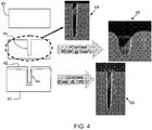
- Figure 4 shows a silicon layer 42 into which a 200nm wide isolated trench 44 is etched, which simulates a small gap of a resonator.
- the wafer is again cured with a hydrogen anneal at 1100°C and 20 Torr for 2 minutes.
- SEM image 44 An SEM image of the trench is shown as SEM image 44, and the resulting profile after the anneal is shown as image 46.
- the trench is first covered with a 5nm thick nitride (protection) layer 48 before it is subjected to the same hydrogen anneal.
- This can be applied by a LPCVD (low pressure chemical vapour deposition) process.
- the resulting profile after the anneal is shown as image 50.
- the image 46 shows that the shape of the trench without the nitride protection layer is changed from its original.
- the trench which is protected by a thin nitride layer before anneal maintains its original shape.
- the high temperatures limit the choice of materials which can be used as device material for the MEMS device.
- most resonators are made of silicon which can withstand the high temperatures used for the hydrogen anneal, particularly if they are protected by for instance by a thin nitride layer as explained above.
- the annealing temperature can be reduced by using SiGe or Ge as a capping layer instead of poly-silicon. In this way the reflow temperature can be lowered to such a level that the SiGe or Ge reflows, but the mono-crystalline Si resonator still remains intact.
- MEMS resonators can be used to substitute crystal oscillators for timing reference purposes.
Description
- This invention relates to MEMS devices, and in particular to the formation of packaged devices.
- MEMS technologies are increasingly being used in integrated circuits. However, numerous product concepts have not been implemented in practice as a result of difficulties providing suitable and cost effective packaging.
- There are many contributing factors to the high costs in packaging of MEMS devices and systems. The three principal factors are:
- proper packaging and efficient assembly of parts and components of sizes less than a few millimetres for MEMS system, with complex geometries, requires special tools and fixtures.
- the high diversity of MEMS devices and systems makes requirements for reliable packaging vary significantly from one product to another. For example, vacuum packing for hermetic sealing is a necessity in many cases.
- the small size of parts and components in MEMS devices and systems creates many unique problems in both packaging and assembly.
- There are a number of techniques used for encapsulating MEMS devices:
- use of off-the-shelf packages and careful handling techniques;
- attachment of a separate cap, usually glass or silicon, on top of a finished MEMS device part;
- integrated wafer level encapsulation.
- The selection of off-the-shelf components is a costly and time-consuming process.
- The use of a separate cap requires a capping wafer, which typically comprises a pre-fabricated cavity formed of glass or silicon. Anodic of frit glass bonding is then used, because of the back-end compatible process temperatures (400°C) in preference to fusion bonding at much higher temperatures (1000°C). A vacuum inside the cavity can be achieved if the bonding is performed in a vacuum chamber. This approach requires wafer bonding and flip-chip alignment equipment.
- An integrated wafer-level solution involves fabricating caps using standard surface micro machining techniques. This approach consumes less area and the chip height is kept lower than if an independently manufactured cap is used. Another advantage of an integrated approach is that the MEMS structure is protected during chip dicing and handling for contamination. If the encapsulation is strong enough, the MEMS chip can be further packaged like a normal IC, which is cost effective. Furthermore this allows the possibility of integration with CMOS processes.
- United States patent application publication number
US2005/0250253 A1 discloses a process for packaging and sealing a microscopic structure device. The process includes the steps of depositing a capping layer of sacrificial material patterned by lithography over the microscopic structure supported on a substrate, depositing a support layer of dielectric material patterned by lithography over the capping layer, providing a plurality of vias through the support layer by lithography, removing the capping layer via wet etching to leave the support layer intact in the form of a shell having a cavity occupied by the microscopic structure, depositing a layer of meltable material over the capping layer that is thick enough to provide a barrier against gas permeation, but thin enough to leave the vias open, and selectively applying a laser beam to the meltable material proximate each via for a sufficient period of time to melt the material for sealing the via. - This invention relates to an integrated approach for forming MEMS device packaging.
- According to the invention, there is provided a method of manufacturing a MEMS device as defined in claim 1.
- This method provides a way of forming a closed cavity over a MEMS device element, using standard fabrication processes. A low number of steps is required - in particular with an anneal process (i.e. heating) in order to cause the at least one opening to close.
- The sacrificial layer can comprise an oxide layer, for example silicon oxide. This can be removed by a standard HF wet etch process or with HF vapour etching.
- The package cover layer preferably comprises silicon, for example polycrystalline silicon or silicon-germanium (SiGe). The hydrogen anneal process closes the at least one opening due to migration of the silicon atoms, but without leaving impurities inside the cavity.
- The package cover layer can have a thickness of between 500nm and 10µm. The diameter of the at least one opening can be selected depending on the number of openings, and may be of the same order of magnitude as the package cover layer thickness.
- Another layer, that can be silicon nitride, can be provided beneath the package cover layer, through which the at least one opening is also formed. This layer is preferably not affected by the anneal process, so that the top surface of the cavity remains smooth and not physically altered by the anneal process.
- The method can further comprise providing an anneal protection layer as part of the process of forming the MEMS device element. This protects the MEMS device (for example a resonator mass, or a flexible contact beam, or a movable capacitor electrode) with a protective layer to prevent damage by the anneal process. The protection layer can comprise silicon nitride.
- Examples of the invention will now be described with reference to the accompanying drawings, in which:
-
Figure 1 shows an example of the manufacturing process in accordance with the invention; -
Figure 2 is used to explain a first experiment used to demonstrate the viability of the invention; -
Figure 3 is used to explain a second experiment used to demonstrate the viability of a second example of method of the invention; and -
Figure 4 is used to explain a third experiment used to demonstrate the viability of a third example of method of the invention. - The invention provides a method of manufacturing a MEMS device in which a closed cavity is formed over the MEMS device element. A sacrificial layer is used, which is removed through holes in a cover layer. The holes are then sealed by an anneal process.
-
Figure 1 shows schematically the method of the invention. -
Figure 1a shows a completed surface-micro machined device, in the form of a resonator in this example. The device comprises asilicon substrate 10, asilicon oxide layer 12 which forms a cavity beneath the resonator mass, and theresonator mass 14 formed in asilicon layer 16. - The manufacture of the MEMS device does not need to be altered by this invention, and any conventional techniques can be used. The MEMS device can be a resonator, capacitor or switch, for example. Typically, the device has a movable portion which needs to be carefully protected by the packaging - in this example the device has a suspended
resonator mass 14. - A
sacrificial layer 20 is deposited and patterned to form an island over the MEMS device, as shown inFigure 1 b. - A
packaging cap layer 22 of poly-silicon is deposited for the formation of the encapsulation shell, andrelease holes 24 are patterned as shown inFigure 1c . - Removal of the
sacrificial layer 20, through therelease holes 24, is provided, to release the mechanical micro structures as shown inFigure 1d . The etching release holes are then sealed by a H2 anneal, to give the structure shown inFigure 1e . - The hydrogen anneal process aims to create a clean silicon (or polysilicon or silicon-germanium) surface. The hydrogen gas does not react with silicon and is proven to desorb efficiently any remaining SiO2. The silicon atoms present on a clean silicon surface can move and have an increasing mobility with higher temperature and lower pressure. Typical conditions for the hydrogen anneal are:
- temperature between 800 and 1150 degrees Celsius (depending on the melting point of the material); and
- low pressure, typically ranging from mTorr to atmospheric pressure.
- The hydrogen gas can be diluted in He or Ar, and preferably has good purity.
- The surface of the capping layer can be cleaned with an HF solution before the anneal process, and ideally the time between the cleaning process and the anneal process should be as short as possible.
- An advantage of the invention is that the release holes 24 are closed without leaving impurities inside the cavity. This allows the design of the positioning of the release holes 24 in such a way that the release is optimal (faster), moreover the release holes can be designed above the resonator which enables a smaller package. Furthermore, it has been found by experimentation that it is possible to seal release holes with a diameter size of 1µm with a
capping layer 22 which is only 1 µm thick. This means that there is a relatively short and wide passageway for the sacrificial etchants, which also will result in a short release time. - The use of a silicon-containing layer means than an H2 anneal will close the release holes due to migration of the silicon atoms but will not leave impurities inside the cavity.
- The operation of the invention has been demonstrated by experiment.
- In a first experiment, release holes in a 1µm polysilicon cap layer were sealed.
-
Figure 2 is a schematic drawing of the experiment. - On a
silicon substrate 30, asilicon nitride layer 32 and asilicon oxide layer 34 are deposited (Figure 2a ). The oxide (sacrificial)layer 34 is patterned (Figure 2b ) and a 1µm thicksilicon cap layer 36 is deposited (Figure 2c ) - Patterning of the release holes 38 in the cap layer is provided (
Figure 2d ), and the sacrificial oxide layer is then removed with an HF-solution or HF-vapor etching (Figure 2e ). The release holes were sealed with a Hydrogen anneal for 2min at 1100°C and a pressure of 20 Torr, to provide the structure shown inFigure 2f . - Analysis of the results, using cross-section SEM images, shows that the cavities which had original release holes of 500nm and 1000nm diameter are completely sealed. If 1500nm diameter release holes are used, the sealing was found to be incomplete, although the size of the release holes decreased. 1000nm diameter release holes are more than adequate to function as release holes for the MEMS devices using a wet etch process.
- A second experiment provided a decrease of the sealing temperature to 1050°C, to show the temperature dependence of the sealing. In this case, the 500nm release holes are still sealed, but the 1000nm release holes are decreased in size but not sealed.
- The capping layer can become rough due to the anneal sealing process. This can increase the height needed inside the cavity for moving of the MEMS device.
-
Figure 3 is used to explain an approach in which a nitride layer (50nm thick for example) is deposited underneath thepolysilicon cap layer 36. -
Figures 3a and 3b correspond toFigures 2a and 2b . - In
Figure 3c , the 50nnmthick nitride layer 40 is deposited, followed by the 1µm thick silicon ascap layer 36 as in the example ofFigure 2 . - The release holes are patterning into the
cap layer 36 and the silicon nitrideprotective layer 40. The sacrificial oxide layer is again removed with an HF-solution (Figure 3e ). - The release holes are then sealed with the hydrogen anneal, for example again 2min at 1100°C and a pressure of 20 Torr.
- The release holes are again sealed in the cap layer, but not in the silicon nitride layer. The silicon nitride layer is not affected, and as a result, the ceiling of the cavity has been shown by experiment to be much smoother than the cavities when no silicon nitride layer is used.
- Because most resonators are made of silicon, the hydrogen anneal can also change the shape of the resonator and so can influence the performance of the resonator.
- One way to address this issue is to provide a protective layer for the resonator parts.
- A further experiment to demonstrate this concept is explained with reference to
Figure 4 . -
Figure 4 shows asilicon layer 42 into which a 200nm wide isolatedtrench 44 is etched, which simulates a small gap of a resonator. The wafer is again cured with a hydrogen anneal at 1100°C and 20 Torr for 2 minutes. - An SEM image of the trench is shown as
SEM image 44, and the resulting profile after the anneal is shown asimage 46. - On another wafer, the trench is first covered with a 5nm thick nitride (protection)
layer 48 before it is subjected to the same hydrogen anneal. This can be applied by a LPCVD (low pressure chemical vapour deposition) process. The resulting profile after the anneal is shown asimage 50. - The
image 46 shows that the shape of the trench without the nitride protection layer is changed from its original. The trench which is protected by a thin nitride layer before anneal maintains its original shape. - The experiments described above show that it is possible to seal release holes up to 1µm. Larger release holes can be sealed if higher temperatures, longer annealing times or thicker capping layers are used. Due to the high process temperatures, the integration of the MEMS device with CMOS processing is limited. The MEMS device has to be encapsulated before the CMOS processing.
- Also, the high temperatures limit the choice of materials which can be used as device material for the MEMS device. However, most resonators are made of silicon which can withstand the high temperatures used for the hydrogen anneal, particularly if they are protected by for instance by a thin nitride layer as explained above.
- The annealing temperature can be reduced by using SiGe or Ge as a capping layer instead of poly-silicon. In this way the reflow temperature can be lowered to such a level that the SiGe or Ge reflows, but the mono-crystalline Si resonator still remains intact.
- One main application of the invention is MEMS resonators. These resonators can be used to substitute crystal oscillators for timing reference purposes.
- Various other applications like gyroscopes and accelerometers will be apparent to those skilled in the art.
Claims (10)
- A method of manufacturing a MEMS device, comprising:forming a MEMS device element (14);forming a sacrificial layer (20;34) over the device element (14);forming a package cover layer (22;36) over the sacrificial layer and which comprises silicon and defines an encapsulation shell;defining at least one opening (24;38) in the package cover layer (22;36);removing the sacrificial layer (20;34) through the at least one opening (24;38), thereby forming a package space over the device element; andsealing the at least one opening (24;38) by a hydrogen anneal process due to migration of the silicon atoms.
- A method as claimed in claim 1, wherein the sacrificial layer (20;34) comprises an oxide layer.
- A method as claimed in claim 2, wherein the sacrificial layer (20;34) comprises silicon oxide.
- A method as claimed in any preceding claim, wherein the package cover layer comprises polycrystalline Silicon-Germanium.
- A method as claimed in any one of claims 1 to 3, wherein the package cover layer (22;36) comprises polycrystalline silicon.
- A method as claimed in any preceding claim, wherein removing the sacrificial layer (20;34) comprises a HF wet etch process or a HF-vapor process.
- A method as claimed in any preceding claim, further comprising providing a silicon nitride layer (40) beneath the package cover layer (36), through which at least one opening is also formed.
- A method as claimed in any preceding claim, further comprising providing an anneal protection layer as part of the process of forming the MEMS device element.
- A method as claimed in claim 8, wherein the protection layer comprises silicon nitride.
- A method as claimed in any preceding claim, wherein the MEMS device element comprises a switch, capacitor or resonator.
Priority Applications (1)
| Application Number | Priority Date | Filing Date | Title |
|---|---|---|---|
| EP09754246.8A EP2297025B1 (en) | 2008-05-28 | 2009-05-19 | Mems devices |
Applications Claiming Priority (3)
| Application Number | Priority Date | Filing Date | Title |
|---|---|---|---|
| EP08104144 | 2008-05-28 | ||
| EP09754246.8A EP2297025B1 (en) | 2008-05-28 | 2009-05-19 | Mems devices |
| PCT/IB2009/052086 WO2009144619A2 (en) | 2008-05-28 | 2009-05-19 | Mems devices |
Publications (2)
| Publication Number | Publication Date |
|---|---|
| EP2297025A2 EP2297025A2 (en) | 2011-03-23 |
| EP2297025B1 true EP2297025B1 (en) | 2016-04-06 |
Family
ID=41377668
Family Applications (1)
| Application Number | Title | Priority Date | Filing Date |
|---|---|---|---|
| EP09754246.8A Not-in-force EP2297025B1 (en) | 2008-05-28 | 2009-05-19 | Mems devices |
Country Status (4)
| Country | Link |
|---|---|
| US (1) | US8481365B2 (en) |
| EP (1) | EP2297025B1 (en) |
| CN (1) | CN102105389A (en) |
| WO (1) | WO2009144619A2 (en) |
Cited By (1)
| Publication number | Priority date | Publication date | Assignee | Title |
|---|---|---|---|---|
| DE102015223399A1 (en) * | 2015-11-26 | 2017-06-01 | Robert Bosch Gmbh | Method for packaging at least one semiconductor device and semiconductor device |
Families Citing this family (15)
| Publication number | Priority date | Publication date | Assignee | Title |
|---|---|---|---|---|
| US8735286B2 (en) * | 2010-10-29 | 2014-05-27 | The Board Of Trustees Of The Leland Stanford Junior University | Deposition-free sealing for micro- and nano-fabrication |
| US9162876B2 (en) * | 2011-03-18 | 2015-10-20 | Stmicroelectronics S.R.L. | Process for manufacturing a membrane microelectromechanical device, and membrane microelectromechanical device |
| CN102303842A (en) * | 2011-08-15 | 2012-01-04 | 上海先进半导体制造股份有限公司 | Pre-packaging method of cover plate compatible with semiconductor process |
| CN103350983B (en) * | 2013-07-01 | 2015-07-15 | 广东合微集成电路技术有限公司 | Integrated wafer-level vacuum packaged MEMS device and manufacturing method thereof |
| EP3019442A4 (en) | 2013-07-08 | 2017-01-25 | Motion Engine Inc. | Mems device and method of manufacturing |
| WO2015042700A1 (en) | 2013-09-24 | 2015-04-02 | Motion Engine Inc. | Mems components and method of wafer-level manufacturing thereof |
| EP3028007A4 (en) | 2013-08-02 | 2017-07-12 | Motion Engine Inc. | Mems motion sensor and method of manufacturing |
| JP6590812B2 (en) | 2014-01-09 | 2019-10-16 | モーション・エンジン・インコーポレーテッド | Integrated MEMS system |
| US20170030788A1 (en) | 2014-04-10 | 2017-02-02 | Motion Engine Inc. | Mems pressure sensor |
| US11674803B2 (en) | 2014-06-02 | 2023-06-13 | Motion Engine, Inc. | Multi-mass MEMS motion sensor |
| US9449867B2 (en) | 2014-06-17 | 2016-09-20 | Taiwan Semiconductor Manufacturing Co., Ltd. | VHF etch barrier for semiconductor integrated microsystem |
| WO2016090467A1 (en) | 2014-12-09 | 2016-06-16 | Motion Engine Inc. | 3d mems magnetometer and associated methods |
| US10407299B2 (en) | 2015-01-15 | 2019-09-10 | Motion Engine Inc. | 3D MEMS device with hermetic cavity |
| US9656859B2 (en) * | 2015-04-16 | 2017-05-23 | The United States Of America, As Represented By The Secretary Of The Navy | Method for fabricating suspended MEMS structures |
| CN112292345A (en) * | 2018-06-13 | 2021-01-29 | 国立大学法人东北大学 | MEMS device manufacturing method and MEMS device |
Citations (2)
| Publication number | Priority date | Publication date | Assignee | Title |
|---|---|---|---|---|
| US20050250253A1 (en) * | 2002-10-23 | 2005-11-10 | Cheung Kin P | Processes for hermetically packaging wafer level microscopic structures |
| US20080049386A1 (en) * | 2006-07-13 | 2008-02-28 | Commissariat A L'energie Atomique | Encapsulated microcomponent equipped with at least one getter |
Family Cites Families (12)
| Publication number | Priority date | Publication date | Assignee | Title |
|---|---|---|---|---|
| US5188983A (en) | 1990-04-11 | 1993-02-23 | Wisconsin Alumni Research Foundation | Polysilicon resonating beam transducers and method of producing the same |
| US5427975A (en) | 1993-05-10 | 1995-06-27 | Delco Electronics Corporation | Method of micromachining an integrated sensor on the surface of a silicon wafer |
| US5716875A (en) * | 1996-03-01 | 1998-02-10 | Motorola, Inc. | Method for making a ferroelectric device |
| US5919364A (en) * | 1996-06-24 | 1999-07-06 | Regents Of The University Of California | Microfabricated filter and shell constructed with a permeable membrane |
| US20070045121A1 (en) | 2002-05-07 | 2007-03-01 | Microfabrica Inc. | Electrochemically fabricated hermetically sealed microstructures and methods of and apparatus for producing such structures |
| US7115436B2 (en) | 2004-02-12 | 2006-10-03 | Robert Bosch Gmbh | Integrated getter area for wafer level encapsulated microelectromechanical systems |
| US7365399B2 (en) | 2006-01-17 | 2008-04-29 | International Business Machines Corporation | Structure and method to form semiconductor-on-pores (SOP) for high device performance and low manufacturing cost |
| US20070235501A1 (en) | 2006-03-29 | 2007-10-11 | John Heck | Self-packaging MEMS device |
| DE102006050188A1 (en) * | 2006-10-25 | 2008-04-30 | Robert Bosch Gmbh | Micromechanical component e.g. inertial sensor, has functional unit with functional surface comprising non-adhesive layer applied on regions, where layer is stable with respect to temperature of above specific value |
| WO2008062350A2 (en) * | 2006-11-20 | 2008-05-29 | Nxp B.V. | A sealing structure and a method of manufacturing the same |
| US7659150B1 (en) * | 2007-03-09 | 2010-02-09 | Silicon Clocks, Inc. | Microshells for multi-level vacuum cavities |
| WO2009130681A2 (en) | 2008-04-23 | 2009-10-29 | Nxp B.V. | Semiconductor device and method of manufacturing a semiconductor device |
-
2009
- 2009-05-19 EP EP09754246.8A patent/EP2297025B1/en not_active Not-in-force
- 2009-05-19 US US12/995,100 patent/US8481365B2/en active Active
- 2009-05-19 WO PCT/IB2009/052086 patent/WO2009144619A2/en active Application Filing
- 2009-05-19 CN CN200980129383XA patent/CN102105389A/en active Pending
Patent Citations (2)
| Publication number | Priority date | Publication date | Assignee | Title |
|---|---|---|---|---|
| US20050250253A1 (en) * | 2002-10-23 | 2005-11-10 | Cheung Kin P | Processes for hermetically packaging wafer level microscopic structures |
| US20080049386A1 (en) * | 2006-07-13 | 2008-02-28 | Commissariat A L'energie Atomique | Encapsulated microcomponent equipped with at least one getter |
Cited By (2)
| Publication number | Priority date | Publication date | Assignee | Title |
|---|---|---|---|---|
| DE102015223399A1 (en) * | 2015-11-26 | 2017-06-01 | Robert Bosch Gmbh | Method for packaging at least one semiconductor device and semiconductor device |
| DE102015223399B4 (en) * | 2015-11-26 | 2018-11-08 | Robert Bosch Gmbh | Method for packaging at least one semiconductor device and semiconductor device |
Also Published As
| Publication number | Publication date |
|---|---|
| EP2297025A2 (en) | 2011-03-23 |
| WO2009144619A2 (en) | 2009-12-03 |
| US8481365B2 (en) | 2013-07-09 |
| US20110198746A1 (en) | 2011-08-18 |
| WO2009144619A3 (en) | 2010-09-16 |
| CN102105389A (en) | 2011-06-22 |
Similar Documents
| Publication | Publication Date | Title |
|---|---|---|
| EP2297025B1 (en) | Mems devices | |
| US8980698B2 (en) | MEMS devices | |
| US7898046B2 (en) | Microelectromechanical systems encapsulation process | |
| EP2327659B1 (en) | Method of manufacturing a semiconductor device and semiconductor devices resulting therefrom | |
| US20120256308A1 (en) | Method for Sealing a Micro-Cavity | |
| US7767484B2 (en) | Method for sealing and backside releasing of microelectromechanical systems | |
| US20080164542A1 (en) | Methods and systems for wafer level packaging of mems structures | |
| US8872359B2 (en) | MEMS devices | |
| US7288464B2 (en) | MEMS packaging structure and methods | |
| EP3606869B1 (en) | Eutectic bonding with alge | |
| US20070298532A1 (en) | Micro-Electro-mechanical (MEMS) encapsulation using buried porous silicon | |
| EP1841688A1 (en) | Packaging of micro devices | |
| US20040166606A1 (en) | Low temperature wafer-level micro-encapsulation | |
| JP5911194B2 (en) | Microelectronic device manufacturing method and device by the method | |
| EP2402284A1 (en) | MEMS manufacturing method | |
| JP2007253265A (en) | Method for manufacturing electric machine element | |
| US20180170748A1 (en) | Semiconductor devices with cavities and methods for fabricating semiconductor devices with cavities | |
| US10584029B2 (en) | Method for producing thin MEMS chips on SOI substrate and micromechanical component | |
| WO2010052682A2 (en) | Mems with poly-silicon cap layer | |
| US20170144883A1 (en) | Microelectronic package and method of manufacturing a microelectronic package |
Legal Events
| Date | Code | Title | Description |
|---|---|---|---|
| PUAI | Public reference made under article 153(3) epc to a published international application that has entered the european phase |
Free format text: ORIGINAL CODE: 0009012 |
|
| AK | Designated contracting states |
Kind code of ref document: A2 Designated state(s): AT BE BG CH CY CZ DE DK EE ES FI FR GB GR HR HU IE IS IT LI LT LU LV MC MK MT NL NO PL PT RO SE SI SK TR |
|
| AX | Request for extension of the european patent |
Extension state: AL BA RS |
|
| 17P | Request for examination filed |
Effective date: 20110316 |
|
| RBV | Designated contracting states (corrected) |
Designated state(s): AT BE BG CH CY CZ DE DK EE ES FI FR GB GR HR HU IE IS IT LI LT LU LV MC MK MT NL NO PL PT RO SE SI SK TR |
|
| DAX | Request for extension of the european patent (deleted) | ||
| 17Q | First examination report despatched |
Effective date: 20150409 |
|
| GRAP | Despatch of communication of intention to grant a patent |
Free format text: ORIGINAL CODE: EPIDOSNIGR1 |
|
| INTG | Intention to grant announced |
Effective date: 20151216 |
|
| GRAS | Grant fee paid |
Free format text: ORIGINAL CODE: EPIDOSNIGR3 |
|
| GRAA | (expected) grant |
Free format text: ORIGINAL CODE: 0009210 |
|
| AK | Designated contracting states |
Kind code of ref document: B1 Designated state(s): AT BE BG CH CY CZ DE DK EE ES FI FR GB GR HR HU IE IS IT LI LT LU LV MC MK MT NL NO PL PT RO SE SI SK TR |
|
| REG | Reference to a national code |
Ref country code: GB Ref legal event code: FG4D |
|
| REG | Reference to a national code |
Ref country code: AT Ref legal event code: REF Ref document number: 787605 Country of ref document: AT Kind code of ref document: T Effective date: 20160415 Ref country code: CH Ref legal event code: EP |
|
| REG | Reference to a national code |
Ref country code: IE Ref legal event code: FG4D |
|
| REG | Reference to a national code |
Ref country code: DE Ref legal event code: R096 Ref document number: 602009037518 Country of ref document: DE |
|
| REG | Reference to a national code |
Ref country code: FR Ref legal event code: PLFP Year of fee payment: 8 |
|
| REG | Reference to a national code |
Ref country code: LT Ref legal event code: MG4D Ref country code: NL Ref legal event code: MP Effective date: 20160406 |
|
| REG | Reference to a national code |
Ref country code: AT Ref legal event code: MK05 Ref document number: 787605 Country of ref document: AT Kind code of ref document: T Effective date: 20160406 |
|
| PG25 | Lapsed in a contracting state [announced via postgrant information from national office to epo] |
Ref country code: BE Free format text: LAPSE BECAUSE OF NON-PAYMENT OF DUE FEES Effective date: 20160531 |
|
| PG25 | Lapsed in a contracting state [announced via postgrant information from national office to epo] |
Ref country code: NL Free format text: LAPSE BECAUSE OF FAILURE TO SUBMIT A TRANSLATION OF THE DESCRIPTION OR TO PAY THE FEE WITHIN THE PRESCRIBED TIME-LIMIT Effective date: 20160406 |
|
| PG25 | Lapsed in a contracting state [announced via postgrant information from national office to epo] |
Ref country code: LT Free format text: LAPSE BECAUSE OF FAILURE TO SUBMIT A TRANSLATION OF THE DESCRIPTION OR TO PAY THE FEE WITHIN THE PRESCRIBED TIME-LIMIT Effective date: 20160406 Ref country code: IS Free format text: LAPSE BECAUSE OF FAILURE TO SUBMIT A TRANSLATION OF THE DESCRIPTION OR TO PAY THE FEE WITHIN THE PRESCRIBED TIME-LIMIT Effective date: 20160806 Ref country code: NO Free format text: LAPSE BECAUSE OF FAILURE TO SUBMIT A TRANSLATION OF THE DESCRIPTION OR TO PAY THE FEE WITHIN THE PRESCRIBED TIME-LIMIT Effective date: 20160706 Ref country code: FI Free format text: LAPSE BECAUSE OF FAILURE TO SUBMIT A TRANSLATION OF THE DESCRIPTION OR TO PAY THE FEE WITHIN THE PRESCRIBED TIME-LIMIT Effective date: 20160406 Ref country code: PL Free format text: LAPSE BECAUSE OF FAILURE TO SUBMIT A TRANSLATION OF THE DESCRIPTION OR TO PAY THE FEE WITHIN THE PRESCRIBED TIME-LIMIT Effective date: 20160406 |
|
| PG25 | Lapsed in a contracting state [announced via postgrant information from national office to epo] |
Ref country code: HR Free format text: LAPSE BECAUSE OF FAILURE TO SUBMIT A TRANSLATION OF THE DESCRIPTION OR TO PAY THE FEE WITHIN THE PRESCRIBED TIME-LIMIT Effective date: 20160406 Ref country code: SE Free format text: LAPSE BECAUSE OF FAILURE TO SUBMIT A TRANSLATION OF THE DESCRIPTION OR TO PAY THE FEE WITHIN THE PRESCRIBED TIME-LIMIT Effective date: 20160406 Ref country code: ES Free format text: LAPSE BECAUSE OF FAILURE TO SUBMIT A TRANSLATION OF THE DESCRIPTION OR TO PAY THE FEE WITHIN THE PRESCRIBED TIME-LIMIT Effective date: 20160406 Ref country code: PT Free format text: LAPSE BECAUSE OF FAILURE TO SUBMIT A TRANSLATION OF THE DESCRIPTION OR TO PAY THE FEE WITHIN THE PRESCRIBED TIME-LIMIT Effective date: 20160808 Ref country code: LV Free format text: LAPSE BECAUSE OF FAILURE TO SUBMIT A TRANSLATION OF THE DESCRIPTION OR TO PAY THE FEE WITHIN THE PRESCRIBED TIME-LIMIT Effective date: 20160406 Ref country code: AT Free format text: LAPSE BECAUSE OF FAILURE TO SUBMIT A TRANSLATION OF THE DESCRIPTION OR TO PAY THE FEE WITHIN THE PRESCRIBED TIME-LIMIT Effective date: 20160406 Ref country code: GR Free format text: LAPSE BECAUSE OF FAILURE TO SUBMIT A TRANSLATION OF THE DESCRIPTION OR TO PAY THE FEE WITHIN THE PRESCRIBED TIME-LIMIT Effective date: 20160707 |
|
| PG25 | Lapsed in a contracting state [announced via postgrant information from national office to epo] |
Ref country code: IT Free format text: LAPSE BECAUSE OF FAILURE TO SUBMIT A TRANSLATION OF THE DESCRIPTION OR TO PAY THE FEE WITHIN THE PRESCRIBED TIME-LIMIT Effective date: 20160406 Ref country code: BE Free format text: LAPSE BECAUSE OF FAILURE TO SUBMIT A TRANSLATION OF THE DESCRIPTION OR TO PAY THE FEE WITHIN THE PRESCRIBED TIME-LIMIT Effective date: 20160406 |
|
| REG | Reference to a national code |
Ref country code: CH Ref legal event code: PL |
|
| REG | Reference to a national code |
Ref country code: DE Ref legal event code: R097 Ref document number: 602009037518 Country of ref document: DE |
|
| PG25 | Lapsed in a contracting state [announced via postgrant information from national office to epo] |
Ref country code: MC Free format text: LAPSE BECAUSE OF FAILURE TO SUBMIT A TRANSLATION OF THE DESCRIPTION OR TO PAY THE FEE WITHIN THE PRESCRIBED TIME-LIMIT Effective date: 20160406 Ref country code: EE Free format text: LAPSE BECAUSE OF FAILURE TO SUBMIT A TRANSLATION OF THE DESCRIPTION OR TO PAY THE FEE WITHIN THE PRESCRIBED TIME-LIMIT Effective date: 20160406 Ref country code: DK Free format text: LAPSE BECAUSE OF FAILURE TO SUBMIT A TRANSLATION OF THE DESCRIPTION OR TO PAY THE FEE WITHIN THE PRESCRIBED TIME-LIMIT Effective date: 20160406 Ref country code: LI Free format text: LAPSE BECAUSE OF NON-PAYMENT OF DUE FEES Effective date: 20160531 Ref country code: CZ Free format text: LAPSE BECAUSE OF FAILURE TO SUBMIT A TRANSLATION OF THE DESCRIPTION OR TO PAY THE FEE WITHIN THE PRESCRIBED TIME-LIMIT Effective date: 20160406 Ref country code: CH Free format text: LAPSE BECAUSE OF NON-PAYMENT OF DUE FEES Effective date: 20160531 Ref country code: SK Free format text: LAPSE BECAUSE OF FAILURE TO SUBMIT A TRANSLATION OF THE DESCRIPTION OR TO PAY THE FEE WITHIN THE PRESCRIBED TIME-LIMIT Effective date: 20160406 Ref country code: RO Free format text: LAPSE BECAUSE OF FAILURE TO SUBMIT A TRANSLATION OF THE DESCRIPTION OR TO PAY THE FEE WITHIN THE PRESCRIBED TIME-LIMIT Effective date: 20160406 |
|
| PLBE | No opposition filed within time limit |
Free format text: ORIGINAL CODE: 0009261 |
|
| STAA | Information on the status of an ep patent application or granted ep patent |
Free format text: STATUS: NO OPPOSITION FILED WITHIN TIME LIMIT |
|
| REG | Reference to a national code |
Ref country code: IE Ref legal event code: MM4A |
|
| 26N | No opposition filed |
Effective date: 20170110 |
|
| GBPC | Gb: european patent ceased through non-payment of renewal fee |
Effective date: 20160706 |
|
| REG | Reference to a national code |
Ref country code: FR Ref legal event code: PLFP Year of fee payment: 9 |
|
| PG25 | Lapsed in a contracting state [announced via postgrant information from national office to epo] |
Ref country code: IE Free format text: LAPSE BECAUSE OF NON-PAYMENT OF DUE FEES Effective date: 20160519 Ref country code: GB Free format text: LAPSE BECAUSE OF NON-PAYMENT OF DUE FEES Effective date: 20160706 Ref country code: SI Free format text: LAPSE BECAUSE OF FAILURE TO SUBMIT A TRANSLATION OF THE DESCRIPTION OR TO PAY THE FEE WITHIN THE PRESCRIBED TIME-LIMIT Effective date: 20160406 |
|
| REG | Reference to a national code |
Ref country code: FR Ref legal event code: PLFP Year of fee payment: 10 |
|
| PG25 | Lapsed in a contracting state [announced via postgrant information from national office to epo] |
Ref country code: HU Free format text: LAPSE BECAUSE OF FAILURE TO SUBMIT A TRANSLATION OF THE DESCRIPTION OR TO PAY THE FEE WITHIN THE PRESCRIBED TIME-LIMIT; INVALID AB INITIO Effective date: 20090519 Ref country code: CY Free format text: LAPSE BECAUSE OF FAILURE TO SUBMIT A TRANSLATION OF THE DESCRIPTION OR TO PAY THE FEE WITHIN THE PRESCRIBED TIME-LIMIT Effective date: 20160406 |
|
| PG25 | Lapsed in a contracting state [announced via postgrant information from national office to epo] |
Ref country code: MT Free format text: LAPSE BECAUSE OF NON-PAYMENT OF DUE FEES Effective date: 20160531 Ref country code: MK Free format text: LAPSE BECAUSE OF FAILURE TO SUBMIT A TRANSLATION OF THE DESCRIPTION OR TO PAY THE FEE WITHIN THE PRESCRIBED TIME-LIMIT Effective date: 20160406 Ref country code: TR Free format text: LAPSE BECAUSE OF FAILURE TO SUBMIT A TRANSLATION OF THE DESCRIPTION OR TO PAY THE FEE WITHIN THE PRESCRIBED TIME-LIMIT Effective date: 20160406 Ref country code: LU Free format text: LAPSE BECAUSE OF NON-PAYMENT OF DUE FEES Effective date: 20160519 |
|
| PG25 | Lapsed in a contracting state [announced via postgrant information from national office to epo] |
Ref country code: BG Free format text: LAPSE BECAUSE OF FAILURE TO SUBMIT A TRANSLATION OF THE DESCRIPTION OR TO PAY THE FEE WITHIN THE PRESCRIBED TIME-LIMIT Effective date: 20160406 |
|
| PGFP | Annual fee paid to national office [announced via postgrant information from national office to epo] |
Ref country code: DE Payment date: 20200421 Year of fee payment: 12 Ref country code: FR Payment date: 20200422 Year of fee payment: 12 |
|
| REG | Reference to a national code |
Ref country code: DE Ref legal event code: R119 Ref document number: 602009037518 Country of ref document: DE |
|
| PG25 | Lapsed in a contracting state [announced via postgrant information from national office to epo] |
Ref country code: DE Free format text: LAPSE BECAUSE OF NON-PAYMENT OF DUE FEES Effective date: 20211201 |
|
| PG25 | Lapsed in a contracting state [announced via postgrant information from national office to epo] |
Ref country code: FR Free format text: LAPSE BECAUSE OF NON-PAYMENT OF DUE FEES Effective date: 20210531 |