EP2295853A1 - Light Emitting Diode Lamp Structure - Google Patents
Light Emitting Diode Lamp Structure Download PDFInfo
- Publication number
- EP2295853A1 EP2295853A1 EP10151349A EP10151349A EP2295853A1 EP 2295853 A1 EP2295853 A1 EP 2295853A1 EP 10151349 A EP10151349 A EP 10151349A EP 10151349 A EP10151349 A EP 10151349A EP 2295853 A1 EP2295853 A1 EP 2295853A1
- Authority
- EP
- European Patent Office
- Prior art keywords
- light emitting
- emitting diode
- diode lamp
- hollow region
- heat dissipating
- Prior art date
- Legal status (The legal status is an assumption and is not a legal conclusion. Google has not performed a legal analysis and makes no representation as to the accuracy of the status listed.)
- Granted
Links
Images


Classifications
-
- F—MECHANICAL ENGINEERING; LIGHTING; HEATING; WEAPONS; BLASTING
- F21—LIGHTING
- F21V—FUNCTIONAL FEATURES OR DETAILS OF LIGHTING DEVICES OR SYSTEMS THEREOF; STRUCTURAL COMBINATIONS OF LIGHTING DEVICES WITH OTHER ARTICLES, NOT OTHERWISE PROVIDED FOR
- F21V29/00—Protecting lighting devices from thermal damage; Cooling or heating arrangements specially adapted for lighting devices or systems
- F21V29/50—Cooling arrangements
- F21V29/70—Cooling arrangements characterised by passive heat-dissipating elements, e.g. heat-sinks
- F21V29/74—Cooling arrangements characterised by passive heat-dissipating elements, e.g. heat-sinks with fins or blades
- F21V29/76—Cooling arrangements characterised by passive heat-dissipating elements, e.g. heat-sinks with fins or blades with essentially identical parallel planar fins or blades, e.g. with comb-like cross-section
-
- F—MECHANICAL ENGINEERING; LIGHTING; HEATING; WEAPONS; BLASTING
- F21—LIGHTING
- F21K—NON-ELECTRIC LIGHT SOURCES USING LUMINESCENCE; LIGHT SOURCES USING ELECTROCHEMILUMINESCENCE; LIGHT SOURCES USING CHARGES OF COMBUSTIBLE MATERIAL; LIGHT SOURCES USING SEMICONDUCTOR DEVICES AS LIGHT-GENERATING ELEMENTS; LIGHT SOURCES NOT OTHERWISE PROVIDED FOR
- F21K9/00—Light sources using semiconductor devices as light-generating elements, e.g. using light-emitting diodes [LED] or lasers
- F21K9/20—Light sources comprising attachment means
- F21K9/23—Retrofit light sources for lighting devices with a single fitting for each light source, e.g. for substitution of incandescent lamps with bayonet or threaded fittings
- F21K9/232—Retrofit light sources for lighting devices with a single fitting for each light source, e.g. for substitution of incandescent lamps with bayonet or threaded fittings specially adapted for generating an essentially omnidirectional light distribution, e.g. with a glass bulb
-
- F—MECHANICAL ENGINEERING; LIGHTING; HEATING; WEAPONS; BLASTING
- F21—LIGHTING
- F21V—FUNCTIONAL FEATURES OR DETAILS OF LIGHTING DEVICES OR SYSTEMS THEREOF; STRUCTURAL COMBINATIONS OF LIGHTING DEVICES WITH OTHER ARTICLES, NOT OTHERWISE PROVIDED FOR
- F21V29/00—Protecting lighting devices from thermal damage; Cooling or heating arrangements specially adapted for lighting devices or systems
- F21V29/50—Cooling arrangements
- F21V29/70—Cooling arrangements characterised by passive heat-dissipating elements, e.g. heat-sinks
- F21V29/74—Cooling arrangements characterised by passive heat-dissipating elements, e.g. heat-sinks with fins or blades
- F21V29/75—Cooling arrangements characterised by passive heat-dissipating elements, e.g. heat-sinks with fins or blades with fins or blades having different shapes, thicknesses or spacing
-
- F—MECHANICAL ENGINEERING; LIGHTING; HEATING; WEAPONS; BLASTING
- F21—LIGHTING
- F21Y—INDEXING SCHEME ASSOCIATED WITH SUBCLASSES F21K, F21L, F21S and F21V, RELATING TO THE FORM OR THE KIND OF THE LIGHT SOURCES OR OF THE COLOUR OF THE LIGHT EMITTED
- F21Y2107/00—Light sources with three-dimensionally disposed light-generating elements
-
- F—MECHANICAL ENGINEERING; LIGHTING; HEATING; WEAPONS; BLASTING
- F21—LIGHTING
- F21Y—INDEXING SCHEME ASSOCIATED WITH SUBCLASSES F21K, F21L, F21S and F21V, RELATING TO THE FORM OR THE KIND OF THE LIGHT SOURCES OR OF THE COLOUR OF THE LIGHT EMITTED
- F21Y2115/00—Light-generating elements of semiconductor light sources
- F21Y2115/10—Light-emitting diodes [LED]
Definitions
- the invention relates to a light emitting diode lamp structure, and more particularly to a lamp structure with better heat dissipation.
- the light emitting diode possessing the advantages of relatively high efficiency, high intensity, cost effectiveness and longer operation life has been increasingly and popularly used in all type of light assembly.
- the level of luminous flux of the LED is characterized not only by its size but also by its heat dissipating efficiency, which is critical.
- the LED in operation accumulates a great deal of heat, which causes the temperature of the LED to rise. High temperature substantially decreases light output efficiency and shortens the service life of the LED.
- the LED structure must include a heat dissipating unit to allow the LED to work in high temperature.
- the LED was manufactured in a similar construction of the light bulb, in which the LED was mounted on a base.
- the base absorbs and transfers the heat generated by the LED to the air.
- the base must embed and electrically engage with a lamp holder. In this case, a part of the base is covered by the lamp holder, and the base could not transfer the heat to the air, further decrease efficiency of the LED.
- heat dissipating is a problem to be solved to improve the performance of the LED.
- a primary object of this invention is to provide a LED lamp structure with brighter light output and higher heat dissipation efficiency.
- the present invention provides a LED lamp structure comprising the features of claim 1.
- Advantageous embodiments are laid down in further claims.
- a lamp according to the invention has a heat dissipating plane, a light emitting housing and a base.
- the heat dissipating plane comprises a plurality of LED elements.
- the light emitting housing further comprises a casing and a first hollow region.
- the heat dissipating plane is partly embedded in the casing and partly revealed through the first hollow region.
- the LED elements are also covered by the casing, and the heat dissipating plane can dissipate heat preferably from the first hollow region.
- the base can be mounted with the light emitting housing. Furthermore, the LED elements can also be electrically engaged with the base.
- the heat dissipating plane may further include some protruded structures, indented structures or other structures that could increase the heat dissipating area.
- the heat dissipating plane may also include a second hollow region.
- the second hollow region can match the first hollow region, which is on the light emitting housing. Air goes through the first hollow region and the second hollow region to form an air cycle. The air cycle could obtain better heat dissipating efficiency.
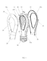
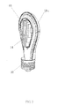
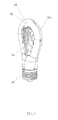
- the light emitting diode (LED) lamp structure constructed in accordance with the present invention has a heat dissipating plane 10, a light emitting housing 20 constructed by two transparent elements 20a, and a base 30.
- the heat dissipating plane 10 is made of thermally conducing material such as aluminum or the like.
- the heat dissipating plane 10 is a racket-like structure, in which the racket-like structure comprises an upper portion 100 and a handle portion 102. Moreover, several LED elements 12 are formed on the periphery of the upper portion 100.
- Each transparent element 20a of the light emitting housing 20, made of glass, acrylic or the like, has a casing 22 and a first hollow region 24 in the center.
- the two transparent elements 20a are confronted and assembled in combination together so that the heat dissipating plane 10 shall be clamped between the two transparent elements 20a.
- the casing 22 covers a plurality of LED elements 12 on the periphery of the upper portion 100. Furthermore, the upper portion 100 of the heat dissipating plane 10 is partly revealed through the first hollow region 24 to obtain better heat dissipating efficiency.
- the heat dissipating plane 10 comprises some first protruded structures 14 as shown in FIGS. 3-4 and/or some first indented structures 16 as shown in FIG 4 .
- the first protruded structure 14 may be a lamellar structure, a schistose structure, a protruded surface or the like.
- the first indented structures 16 may be a grid-like structure, a wave-like structure, a flake-like structure or the like.
- the first protruded structures 14 and/or the first indented structures 16 may be revealed through the first hollow region 24 in order to increase the overall heat dissipating area and improve heat dissipation.
- Each transparent element 20a on an outer surface has one or more second protruded structures 26 as shown in FIG 3 or second indented structures 28 as shown in FIG 4 to increase the overall heat dissipating area and dissipate heat efficiently.
- the second protruded structure 26 may be a lamellar structure, a schistose structure, a protruded surface or the like.
- the second indented structures 28 may be a grid-like structure, a wave-like structure, a flake-like structure or the like.
- the base 30 is made of conducting material and has a metal screw type base.
- the base 30 is positioned below the handle portion 102 of the heat dissipating plane 10 and is mounted with the two transparent elements 20a.
- the transparent elements 20a can be engaged or cohered to the base 30.
- Each transparent element 20a comprises a neck portion 23, which assembles with an opening 32 of the base 30.
- the base 30 may also be electrically engaged with the LED elements 12. For instance, when the base 30 is mounted on a lamp holder (not shown) the current flows to the base 30 so that the LED elements 12 start operating.
- the heat dissipating plane 10 may absorb the heat generated by the LED elements 12 and then dissipate the heat by itself and by the first protruded structures 14 and/or the first indented structures 16.
- the transparent elements 20a also dissipate heat and allow the LED elements 12 to operate in a relatively low temperature.
- the heat dissipating plane 10 can be shaped so that a plurality of LED elements 12 can be formed not only on the periphery of the heat dissipating plane 10 but also at any place on the sides of the heat dissipating plane 10. In this case, the different position of the LED elements 12 may alter the light projection angle not being limited to a certain range.
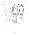
- Figs. 5-7 show a LED lamp structure constructed according to the third embodiment of the present invention.
- the heat dissipating plane 10 comprises a second hollow region 18 relatively corresponded with the first hollow region 24 to have the LED lamp structure provided with a fully penetrating structure constructed from the second hollow region 18 in combination with the first hollow region 24.
- the second hollow region 18 can also increase the heat dissipating area of the heat dissipating plane 10.
- this embodiment allows the LED to generate higher light output without adverse temperature-related effects.
- the heat dissipating plane 10 also has one or more third dissipating structures 19 revealed through the second hollow region 18 in order to increase the overall heat dissipating area and dissipate heat efficiently.
- the third dissipating structure 19 if constructed by a protruded structure may be a lamellar structure, a schistose structure, a protruded surface or the like, or if constructed by an indented structure may be a grid-like structure, a wave-like structure, a flake-like structure or the like.
- the second hollow region 18 can also be a grid structure.
- the LED lamp structure may dissipate more heat into the air.
- the heat dissipating plane 10 may be formed as an element of substantially constant thickness. It may be formed e.g. from sheet material and have a racket-like structure as shown in Fig. 1 . However, other shapes with a through opening are also possible.
- the transparent elements 20a have a corresponding shape with an opening corresponding to the through opening of the afore-mentioned heat dissipating element.
- the two transparent elements 20a define two shells of a housing 20 around the heat dissipating element. However, a portion of the heat dissipating element is partly exposed to the exterior, i.e. remains uncovered to obtain better heat dissipating efficiency.
- the uncovered portion faces towards the opening while the radially outer rim of the dissipating element is covered by the housing 20.
- Protruding structures formed or provided on the dissipating element may extend into the opening.
- the uncovered part of the heat dissipating element may face radially outwardly.
- the lamp may have an inner and outer rim of the heat dissipating element or protruded portions thereof or thereon exposed to the exterior while the remaining portions are shielded by a transparent housing, which may be formed in one or more pieces, preferably two substantially symmetric shells.
Landscapes
- Engineering & Computer Science (AREA)
- General Engineering & Computer Science (AREA)
- Physics & Mathematics (AREA)
- Geometry (AREA)
- Microelectronics & Electronic Packaging (AREA)
- Optics & Photonics (AREA)
- Arrangement Of Elements, Cooling, Sealing, Or The Like Of Lighting Devices (AREA)
- Non-Portable Lighting Devices Or Systems Thereof (AREA)
Abstract
Description
- The invention relates to a light emitting diode lamp structure, and more particularly to a lamp structure with better heat dissipation.
- The light emitting diode (LED) possessing the advantages of relatively high efficiency, high intensity, cost effectiveness and longer operation life has been increasingly and popularly used in all type of light assembly.
- The level of luminous flux of the LED is characterized not only by its size but also by its heat dissipating efficiency, which is critical. The LED in operation accumulates a great deal of heat, which causes the temperature of the LED to rise. High temperature substantially decreases light output efficiency and shortens the service life of the LED. Thus, in prior invent the LED structure must include a heat dissipating unit to allow the LED to work in high temperature.
- Conventionally, the LED was manufactured in a similar construction of the light bulb, in which the LED was mounted on a base. When the LED is in operation, the base absorbs and transfers the heat generated by the LED to the air. Moreover, to provide electric power to the LED, the base must embed and electrically engage with a lamp holder. In this case, a part of the base is covered by the lamp holder, and the base could not transfer the heat to the air, further decrease efficiency of the LED.
- Thus, heat dissipating is a problem to be solved to improve the performance of the LED.
- According to the aforesaid shortcoming, a primary object of this invention is to provide a LED lamp structure with brighter light output and higher heat dissipation efficiency.
- To achieve this objective, the present invention provides a LED lamp structure comprising the features of claim 1. Advantageous embodiments are laid down in further claims.
- A lamp according to the invention has a heat dissipating plane, a light emitting housing and a base. The heat dissipating plane comprises a plurality of LED elements. In addition, the light emitting housing further comprises a casing and a first hollow region. The heat dissipating plane is partly embedded in the casing and partly revealed through the first hollow region. The LED elements are also covered by the casing, and the heat dissipating plane can dissipate heat preferably from the first hollow region. The base can be mounted with the light emitting housing. Furthermore, the LED elements can also be electrically engaged with the base.
- The heat dissipating plane may further include some protruded structures, indented structures or other structures that could increase the heat dissipating area.
- The heat dissipating plane may also include a second hollow region. The second hollow region can match the first hollow region, which is on the light emitting housing. Air goes through the first hollow region and the second hollow region to form an air cycle. The air cycle could obtain better heat dissipating efficiency.
- Representative advantages offered by this invention may be briefly summarized below.
- (1) The present invention which includes a plurality of LEDs enabled to increase brightness.
- (2) The present invention increases efficiency of heat dissipation and heat conductivity, thus effectively avoiding the problem of thermal degradation of LEDs.
- These and other features of the invention will be described in further detail in the following detailed description of a presently preferred embodiment.
- The technical means adopted by the present invention to achieve the above and other objects can be best understood by referring to the following detailed description of the preferred embodiments and the accompanying drawings, in which:
-
FIG 1 is an exploded view of a LED lamp structure according to a first embodiment of present invention; -
FIG .2 is a partly assembled perspective view of a LED lamp structure according to a first embodiment of the present invention; -
FIG .3 is a perspective view of a LED lamp structure according to a first embodiment of the present invention; -
FIG .4 is a perspective view of a LED lamp structure according to a second embodiment of the present invention; -
FIG 5 is an exploded view of LED lamp structure according to a third embodiment of present invention; -
FIG .6 is a partly assembled perspective view of a LED lamp structure according to a third embodiment of the present invention; -
FIG7 is a perspective view of a LED lamp structure according to a third embodiment of the present invention; -
FIG .8 is a perspective view of a LED lamp structure according to a fourth embodiment of the present invention. - An exemplary embodiment of present invention will hereinafter be described in detail with reference to the accompanying drawing. As those skilled in the art would realize, the described embodiments may be modified in various different ways, all without departing from the spirit or scope of the present invention.
- Referring to
FIGS. 1-3 , the light emitting diode (LED) lamp structure constructed in accordance with the present invention has aheat dissipating plane 10, alight emitting housing 20 constructed by twotransparent elements 20a, and abase 30. - The
heat dissipating plane 10 is made of thermally conducing material such as aluminum or the like. Theheat dissipating plane 10 is a racket-like structure, in which the racket-like structure comprises anupper portion 100 and ahandle portion 102. Moreover,several LED elements 12 are formed on the periphery of theupper portion 100. - Each
transparent element 20a of thelight emitting housing 20, made of glass, acrylic or the like, has acasing 22 and a firsthollow region 24 in the center. The twotransparent elements 20a are confronted and assembled in combination together so that the heatdissipating plane 10 shall be clamped between the twotransparent elements 20a. Thecasing 22 covers a plurality ofLED elements 12 on the periphery of theupper portion 100. Furthermore, theupper portion 100 of theheat dissipating plane 10 is partly revealed through the firsthollow region 24 to obtain better heat dissipating efficiency. - Further, the heat
dissipating plane 10 comprises some firstprotruded structures 14 as shown inFIGS. 3-4 and/or some firstindented structures 16 as shown inFIG 4 . The firstprotruded structure 14 may be a lamellar structure, a schistose structure, a protruded surface or the like. The firstindented structures 16 may be a grid-like structure, a wave-like structure, a flake-like structure or the like. - The first
protruded structures 14 and/or the firstindented structures 16 may be revealed through the firsthollow region 24 in order to increase the overall heat dissipating area and improve heat dissipation. - Furthermore, heat generated from the
LED elements 12 could be dissipate through thetransparent elements 20a. Eachtransparent element 20a on an outer surface has one or more secondprotruded structures 26 as shown inFIG 3 or secondindented structures 28 as shown inFIG 4 to increase the overall heat dissipating area and dissipate heat efficiently. The secondprotruded structure 26 may be a lamellar structure, a schistose structure, a protruded surface or the like. The secondindented structures 28 may be a grid-like structure, a wave-like structure, a flake-like structure or the like. - The
base 30 is made of conducting material and has a metal screw type base. Thebase 30 is positioned below thehandle portion 102 of theheat dissipating plane 10 and is mounted with the twotransparent elements 20a. Thetransparent elements 20a can be engaged or cohered to thebase 30. Eachtransparent element 20a comprises aneck portion 23, which assembles with anopening 32 of thebase 30. Thebase 30 may also be electrically engaged with theLED elements 12. For instance, when thebase 30 is mounted on a lamp holder (not shown) the current flows to thebase 30 so that theLED elements 12 start operating. - When the current flows though the
LED elements 12, theLED elements 12 emit light and generate heat. Theheat dissipating plane 10 may absorb the heat generated by theLED elements 12 and then dissipate the heat by itself and by the firstprotruded structures 14 and/or the firstindented structures 16. Thetransparent elements 20a also dissipate heat and allow theLED elements 12 to operate in a relatively low temperature. Furthermore, theheat dissipating plane 10 can be shaped so that a plurality ofLED elements 12 can be formed not only on the periphery of theheat dissipating plane 10 but also at any place on the sides of theheat dissipating plane 10. In this case, the different position of theLED elements 12 may alter the light projection angle not being limited to a certain range. -
Figs. 5-7 show a LED lamp structure constructed according to the third embodiment of the present invention. The following description focuses on the main differences between the first embodiment and the third embodiment. According to this embodiment, theheat dissipating plane 10 comprises a secondhollow region 18 relatively corresponded with the firsthollow region 24 to have the LED lamp structure provided with a fully penetrating structure constructed from the secondhollow region 18 in combination with the firsthollow region 24. Furthermore, the secondhollow region 18 can also increase the heat dissipating area of theheat dissipating plane 10. In addition, this embodiment allows the LED to generate higher light output without adverse temperature-related effects. Besides, theheat dissipating plane 10 also has one or more third dissipatingstructures 19 revealed through the secondhollow region 18 in order to increase the overall heat dissipating area and dissipate heat efficiently. The third dissipatingstructure 19 if constructed by a protruded structure may be a lamellar structure, a schistose structure, a protruded surface or the like, or if constructed by an indented structure may be a grid-like structure, a wave-like structure, a flake-like structure or the like. - As shows in
FIG 8 , the secondhollow region 18 can also be a grid structure. With the grid structure, the LED lamp structure may dissipate more heat into the air. - Generally, the
heat dissipating plane 10 may be formed as an element of substantially constant thickness. It may be formed e.g. from sheet material and have a racket-like structure as shown inFig. 1 . However, other shapes with a through opening are also possible. Thetransparent elements 20a have a corresponding shape with an opening corresponding to the through opening of the afore-mentioned heat dissipating element. The twotransparent elements 20a define two shells of ahousing 20 around the heat dissipating element. However, a portion of the heat dissipating element is partly exposed to the exterior, i.e. remains uncovered to obtain better heat dissipating efficiency. Preferably, the uncovered portion faces towards the opening while the radially outer rim of the dissipating element is covered by thehousing 20. Protruding structures formed or provided on the dissipating element may extend into the opening. However, it is also possible to arrange the uncovered part of the heat dissipating element to face radially outwardly. Also, the lamp may have an inner and outer rim of the heat dissipating element or protruded portions thereof or thereon exposed to the exterior while the remaining portions are shielded by a transparent housing, which may be formed in one or more pieces, preferably two substantially symmetric shells. These features may be applied partly or in full to the afore-mentioned embodiments to modify them. - The present invention has been demonstrated herein by reference to the preferred embodiments. However, it is understood that the embodiments are not intended to limit the scope of the present invention, which is defined by the appended claims.
Claims (10)
- A light emitting diode lamp structure, comprising:- a heat dissipating plane (10) having a plurality of light emitting diodes;- a light emitting housing (20) constructed by two transparent elements (20a) each defining a casing (22) and a first hollow region (24), wherein the heat dissipation plane (10) is partly covered by the light emitting housing (20) and partly revealed through the first hollow region (24), and the light emitting diodes are covered by the light emitting housing (20); and- a base (30) mounted with the light emitting housing (20) and electrically engaged with the light emitting diodes.
- The light emitting diode lamp structure as cited in Claim 1, characterized in that the heat dissipating plate (10) further comprises first protruded structures (14) and/or first indented structures (16) revealed through the first hollow region (24).
- The light emitting diode lamp structure as cited in Claim 2, characterized in that the first protruded structures (14) is a lamellar structure, a schistose structure or a protruded surface, and the first indented structure (16) is a grid-like structure, a wave-like structure or a flake-like structure.
- The light emitting diode lamp structure as cited in one of Claims 1 to 3, characterized in that the heat dissipating plane (10) further comprises a second hollow region (18) relatively corresponded with the first hollow region (24) of the light emitting housing (20).
- The light emitting diode lamp structure as cited in Claim 4, characterized in that the second hollow region (18) is a through hole or a grid structure.
- The light emitting diode lamp structure as cited in Claim 4 or 5, characterized in that a surface of the second hollow region (18) further comprises one or more third dissipating structures (19).
- The light emitting diode lamp structure as cited in Claim 6, characterized in that the third dissipating structures (19) is either a protrude structure including a lamellar structure, a schistose structure or a protruded surface or an indented structure including a grid-like structure, a wave-like structure or a flake-like structure.
- The light emitting diode lamp structure as cited in one of Claims 1 to 7, characterized in that the light emitting housing is made of glass or acrylic.
- The light emitting diode lamp structure as cited in one of Claims 1 to 8, characterized in that the transparent element (20a) on an outer surface further comprises one or more second protruded structures (26) or second indented structures (28).
- The light emitting diode lamp structure as cited in Claim 9, characterized in that the second protruded structure (26) is a lamellar structure, a schistose structure or a protruded surface, and the second indented structures (28) is a grid-like structure, a wave-like structure or a flake-like structure.
Applications Claiming Priority (1)
| Application Number | Priority Date | Filing Date | Title |
|---|---|---|---|
| TW098130990A TW201109579A (en) | 2009-09-15 | 2009-09-15 | Structure of LED lamp |
Publications (2)
| Publication Number | Publication Date |
|---|---|
| EP2295853A1 true EP2295853A1 (en) | 2011-03-16 |
| EP2295853B1 EP2295853B1 (en) | 2013-05-08 |
Family
ID=43017107
Family Applications (1)
| Application Number | Title | Priority Date | Filing Date |
|---|---|---|---|
| EP10151349.7A Active EP2295853B1 (en) | 2009-09-15 | 2010-01-21 | Light Emitting Diode Lamp Structure |
Country Status (4)
| Country | Link |
|---|---|
| US (1) | US8425086B2 (en) |
| EP (1) | EP2295853B1 (en) |
| JP (1) | JP3158176U (en) |
| TW (1) | TW201109579A (en) |
Cited By (1)
| Publication number | Priority date | Publication date | Assignee | Title |
|---|---|---|---|---|
| WO2014087366A1 (en) * | 2012-12-05 | 2014-06-12 | Koninklijke Philips N.V. | Flat lighting device |
Families Citing this family (13)
| Publication number | Priority date | Publication date | Assignee | Title |
|---|---|---|---|---|
| US9222632B2 (en) * | 2013-01-31 | 2015-12-29 | Cree, Inc. | LED lighting fixture |
| US9028087B2 (en) | 2006-09-30 | 2015-05-12 | Cree, Inc. | LED light fixture |
| US7686469B2 (en) | 2006-09-30 | 2010-03-30 | Ruud Lighting, Inc. | LED lighting fixture |
| US20090086491A1 (en) | 2007-09-28 | 2009-04-02 | Ruud Lighting, Inc. | Aerodynamic LED Floodlight Fixture |
| EP2623846B8 (en) * | 2009-05-28 | 2016-09-21 | Philips Lighting Holding B.V. | Illumination device and method for assembly of an illumination device |
| JP5670936B2 (en) * | 2012-02-27 | 2015-02-18 | 株式会社東芝 | Lighting device |
| US9010964B2 (en) * | 2012-04-26 | 2015-04-21 | Epistar Corporation | LED light bulb with interior facing LEDs |
| CN104406069A (en) * | 2012-12-28 | 2015-03-11 | 四川新力光源股份有限公司 | LED (light-emitting diode) lamp and LED, particularly substitute LED |
| US9068732B2 (en) * | 2013-03-29 | 2015-06-30 | Uniled Lighting Tw., Inc | Air-cooled LED lamp bulb |
| RU2654203C1 (en) * | 2014-07-24 | 2018-05-17 | Филипс Лайтинг Холдинг Б.В. | Lamp and lighting device |
| CN106662302B (en) * | 2014-09-02 | 2019-11-19 | 飞利浦灯具控股公司 | lighting device |
| WO2017013141A1 (en) | 2015-07-20 | 2017-01-26 | Philips Lighting Holding B.V. | Lighting device with light guide |
| TR201617051A2 (en) * | 2016-11-23 | 2017-01-23 | Ttaf Elektronik Sanayi Ve Ticaret Ltd Sirketi | PLASTIC LIGHTING FIXTURE WITH MAIN BODY |
Citations (4)
| Publication number | Priority date | Publication date | Assignee | Title |
|---|---|---|---|---|
| EP1895232A1 (en) * | 2006-08-29 | 2008-03-05 | Topson Optoelectronics Semi-conductor Co., Ltd. | Improved heat sink structure for light-emitting diode based streetlamp |
| DE102007037820A1 (en) * | 2007-08-10 | 2009-02-12 | Osram Gesellschaft mit beschränkter Haftung | Led lamp |
| WO2009091562A2 (en) | 2008-01-15 | 2009-07-23 | Philip Premysler | Omnidirectional led light bulb |
| US20090225554A1 (en) * | 2008-03-05 | 2009-09-10 | Li-Hong Technological, Co., Ltd. | Improved Heat-Dissipation Structure |
Family Cites Families (11)
| Publication number | Priority date | Publication date | Assignee | Title |
|---|---|---|---|---|
| KR200350484Y1 (en) * | 2004-02-06 | 2004-05-13 | 주식회사 대진디엠피 | Corn Type LED Light |
| US7658510B2 (en) * | 2004-08-18 | 2010-02-09 | Remco Solid State Lighting Inc. | System and method for power control in a LED luminaire |
| US7641361B2 (en) * | 2007-05-24 | 2010-01-05 | Brasstech, Inc. | Light emitting diode lamp |
| CN101329054B (en) * | 2007-06-22 | 2010-09-29 | 富准精密工业(深圳)有限公司 | LED lamp with heat radiation structure |
| US7434964B1 (en) * | 2007-07-12 | 2008-10-14 | Fu Zhun Precision Industry (Shen Zhen) Co., Ltd. | LED lamp with a heat sink assembly |
| CN101368719B (en) * | 2007-08-13 | 2011-07-06 | 太一节能系统股份有限公司 | LED lamps |
| CN101373064B (en) * | 2007-08-24 | 2011-05-11 | 富准精密工业(深圳)有限公司 | LED light fitting |
| CN101614383A (en) * | 2008-06-27 | 2009-12-30 | 富准精密工业(深圳)有限公司 | LED lamp |
| KR100902631B1 (en) * | 2008-10-24 | 2009-06-12 | 현대통신 주식회사 | LED light emitting lamp of circular structure using nanospreader |
| US9030120B2 (en) * | 2009-10-20 | 2015-05-12 | Cree, Inc. | Heat sinks and lamp incorporating same |
| US20110115358A1 (en) * | 2009-11-16 | 2011-05-19 | Led Folio Corporation | Led bulb having side-emitting led modules with heatsinks therebetween |
-
2009
- 2009-09-15 TW TW098130990A patent/TW201109579A/en unknown
- 2009-12-10 US US12/635,439 patent/US8425086B2/en active Active
-
2010
- 2010-01-06 JP JP2010000049U patent/JP3158176U/en not_active Expired - Lifetime
- 2010-01-21 EP EP10151349.7A patent/EP2295853B1/en active Active
Patent Citations (4)
| Publication number | Priority date | Publication date | Assignee | Title |
|---|---|---|---|---|
| EP1895232A1 (en) * | 2006-08-29 | 2008-03-05 | Topson Optoelectronics Semi-conductor Co., Ltd. | Improved heat sink structure for light-emitting diode based streetlamp |
| DE102007037820A1 (en) * | 2007-08-10 | 2009-02-12 | Osram Gesellschaft mit beschränkter Haftung | Led lamp |
| WO2009091562A2 (en) | 2008-01-15 | 2009-07-23 | Philip Premysler | Omnidirectional led light bulb |
| US20090225554A1 (en) * | 2008-03-05 | 2009-09-10 | Li-Hong Technological, Co., Ltd. | Improved Heat-Dissipation Structure |
Cited By (5)
| Publication number | Priority date | Publication date | Assignee | Title |
|---|---|---|---|---|
| WO2014087366A1 (en) * | 2012-12-05 | 2014-06-12 | Koninklijke Philips N.V. | Flat lighting device |
| JP2015537354A (en) * | 2012-12-05 | 2015-12-24 | コーニンクレッカ フィリップス エヌ ヴェKoninklijke Philips N.V. | Flat lighting equipment |
| JP2016500462A (en) * | 2012-12-05 | 2016-01-12 | コーニンクレッカ フィリップス エヌ ヴェKoninklijke Philips N.V. | Flat lighting equipment |
| JP2016504723A (en) * | 2012-12-05 | 2016-02-12 | コーニンクレッカ フィリップス エヌ ヴェKoninklijke Philips N.V. | Flat lighting equipment |
| US9732912B2 (en) | 2012-12-05 | 2017-08-15 | Philips Lighting Holding B.V. | Flat lighting device |
Also Published As
| Publication number | Publication date |
|---|---|
| US8425086B2 (en) | 2013-04-23 |
| TW201109579A (en) | 2011-03-16 |
| US20110062847A1 (en) | 2011-03-17 |
| EP2295853B1 (en) | 2013-05-08 |
| JP3158176U (en) | 2010-03-18 |
Similar Documents
| Publication | Publication Date | Title |
|---|---|---|
| EP2295853B1 (en) | Light Emitting Diode Lamp Structure | |
| JP4917697B2 (en) | Lamp and lighting device | |
| EP2397753B1 (en) | Led lamp and a heat sink thereof having a wound heat pipe | |
| CN202834855U (en) | LED (light-emitting diode) lighting equipment with separated driving circuit | |
| US8304971B2 (en) | LED light bulb with a multidirectional distribution and novel heat dissipating structure | |
| EP2444724A1 (en) | LED bulb | |
| TW201348646A (en) | Light emitting diode lamp | |
| WO2011081574A2 (en) | Light-emitting diode lamp | |
| JP2012195076A (en) | Illumination device | |
| JP2017130475A (en) | Luminaire | |
| KR200456131Y1 (en) | LED floodlight | |
| KR20110003221U (en) | Led light | |
| TWI537522B (en) | Light-emitting device | |
| JP3112794U (en) | Radiator for light-emitting diode lamp | |
| KR200457373Y1 (en) | LED lamp structure | |
| JP2014170672A (en) | Illumination device | |
| KR20100099520A (en) | Illuminator | |
| JP2013110198A (en) | Light emitting diode lamp | |
| JP6146712B2 (en) | lamp | |
| TWI392830B (en) | Led lamp assembly | |
| JP6136196B2 (en) | lamp | |
| KR101823135B1 (en) | Lighting device | |
| JP3158964U (en) | LED lighting device | |
| CN202165859U (en) | High-power LED (light-emitting diode) integral lighting source | |
| JP6003539B2 (en) | Lamp device |
Legal Events
| Date | Code | Title | Description |
|---|---|---|---|
| PUAI | Public reference made under article 153(3) epc to a published international application that has entered the european phase |
Free format text: ORIGINAL CODE: 0009012 |
|
| AK | Designated contracting states |
Kind code of ref document: A1 Designated state(s): AT BE BG CH CY CZ DE DK EE ES FI FR GB GR HR HU IE IS IT LI LT LU LV MC MK MT NL NO PL PT RO SE SI SK SM TR |
|
| AX | Request for extension of the european patent |
Extension state: AL BA RS |
|
| 17P | Request for examination filed |
Effective date: 20110915 |
|
| GRAC | Information related to communication of intention to grant a patent modified |
Free format text: ORIGINAL CODE: EPIDOSCIGR1 |
|
| GRAP | Despatch of communication of intention to grant a patent |
Free format text: ORIGINAL CODE: EPIDOSNIGR1 |
|
| RIC1 | Information provided on ipc code assigned before grant |
Ipc: F21Y 101/02 20060101ALN20120906BHEP Ipc: F21V 29/00 20060101AFI20120906BHEP Ipc: F21K 99/00 20100101ALI20120906BHEP |
|
| GRAS | Grant fee paid |
Free format text: ORIGINAL CODE: EPIDOSNIGR3 |
|
| GRAP | Despatch of communication of intention to grant a patent |
Free format text: ORIGINAL CODE: EPIDOSNIGR1 |
|
| RIC1 | Information provided on ipc code assigned before grant |
Ipc: F21Y 101/02 20060101ALN20130222BHEP Ipc: F21K 99/00 20100101ALI20130222BHEP Ipc: F21V 29/00 20060101AFI20130222BHEP |
|
| GRAA | (expected) grant |
Free format text: ORIGINAL CODE: 0009210 |
|
| AK | Designated contracting states |
Kind code of ref document: B1 Designated state(s): AT BE BG CH CY CZ DE DK EE ES FI FR GB GR HR HU IE IS IT LI LT LU LV MC MK MT NL NO PL PT RO SE SI SK SM TR |
|
| REG | Reference to a national code |
Ref country code: GB Ref legal event code: FG4D |
|
| REG | Reference to a national code |
Ref country code: CH Ref legal event code: EP Ref country code: AT Ref legal event code: REF Ref document number: 611275 Country of ref document: AT Kind code of ref document: T Effective date: 20130515 |
|
| REG | Reference to a national code |
Ref country code: IE Ref legal event code: FG4D |
|
| REG | Reference to a national code |
Ref country code: DE Ref legal event code: R096 Ref document number: 602010006870 Country of ref document: DE Effective date: 20130704 |
|
| REG | Reference to a national code |
Ref country code: AT Ref legal event code: MK05 Ref document number: 611275 Country of ref document: AT Kind code of ref document: T Effective date: 20130508 |
|
| REG | Reference to a national code |
Ref country code: LT Ref legal event code: MG4D |
|
| REG | Reference to a national code |
Ref country code: NL Ref legal event code: VDEP Effective date: 20130508 |
|
| PG25 | Lapsed in a contracting state [announced via postgrant information from national office to epo] |
Ref country code: FI Free format text: LAPSE BECAUSE OF FAILURE TO SUBMIT A TRANSLATION OF THE DESCRIPTION OR TO PAY THE FEE WITHIN THE PRESCRIBED TIME-LIMIT Effective date: 20130508 Ref country code: IS Free format text: LAPSE BECAUSE OF FAILURE TO SUBMIT A TRANSLATION OF THE DESCRIPTION OR TO PAY THE FEE WITHIN THE PRESCRIBED TIME-LIMIT Effective date: 20130908 Ref country code: GR Free format text: LAPSE BECAUSE OF FAILURE TO SUBMIT A TRANSLATION OF THE DESCRIPTION OR TO PAY THE FEE WITHIN THE PRESCRIBED TIME-LIMIT Effective date: 20130809 Ref country code: ES Free format text: LAPSE BECAUSE OF FAILURE TO SUBMIT A TRANSLATION OF THE DESCRIPTION OR TO PAY THE FEE WITHIN THE PRESCRIBED TIME-LIMIT Effective date: 20130819 Ref country code: LT Free format text: LAPSE BECAUSE OF FAILURE TO SUBMIT A TRANSLATION OF THE DESCRIPTION OR TO PAY THE FEE WITHIN THE PRESCRIBED TIME-LIMIT Effective date: 20130508 Ref country code: NO Free format text: LAPSE BECAUSE OF FAILURE TO SUBMIT A TRANSLATION OF THE DESCRIPTION OR TO PAY THE FEE WITHIN THE PRESCRIBED TIME-LIMIT Effective date: 20130808 Ref country code: SE Free format text: LAPSE BECAUSE OF FAILURE TO SUBMIT A TRANSLATION OF THE DESCRIPTION OR TO PAY THE FEE WITHIN THE PRESCRIBED TIME-LIMIT Effective date: 20130508 Ref country code: PT Free format text: LAPSE BECAUSE OF FAILURE TO SUBMIT A TRANSLATION OF THE DESCRIPTION OR TO PAY THE FEE WITHIN THE PRESCRIBED TIME-LIMIT Effective date: 20130909 Ref country code: AT Free format text: LAPSE BECAUSE OF FAILURE TO SUBMIT A TRANSLATION OF THE DESCRIPTION OR TO PAY THE FEE WITHIN THE PRESCRIBED TIME-LIMIT Effective date: 20130508 Ref country code: SI Free format text: LAPSE BECAUSE OF FAILURE TO SUBMIT A TRANSLATION OF THE DESCRIPTION OR TO PAY THE FEE WITHIN THE PRESCRIBED TIME-LIMIT Effective date: 20130508 |
|
| PG25 | Lapsed in a contracting state [announced via postgrant information from national office to epo] |
Ref country code: BG Free format text: LAPSE BECAUSE OF FAILURE TO SUBMIT A TRANSLATION OF THE DESCRIPTION OR TO PAY THE FEE WITHIN THE PRESCRIBED TIME-LIMIT Effective date: 20130808 Ref country code: PL Free format text: LAPSE BECAUSE OF FAILURE TO SUBMIT A TRANSLATION OF THE DESCRIPTION OR TO PAY THE FEE WITHIN THE PRESCRIBED TIME-LIMIT Effective date: 20130508 Ref country code: CY Free format text: LAPSE BECAUSE OF FAILURE TO SUBMIT A TRANSLATION OF THE DESCRIPTION OR TO PAY THE FEE WITHIN THE PRESCRIBED TIME-LIMIT Effective date: 20130508 Ref country code: HR Free format text: LAPSE BECAUSE OF FAILURE TO SUBMIT A TRANSLATION OF THE DESCRIPTION OR TO PAY THE FEE WITHIN THE PRESCRIBED TIME-LIMIT Effective date: 20130508 |
|
| PG25 | Lapsed in a contracting state [announced via postgrant information from national office to epo] |
Ref country code: LV Free format text: LAPSE BECAUSE OF FAILURE TO SUBMIT A TRANSLATION OF THE DESCRIPTION OR TO PAY THE FEE WITHIN THE PRESCRIBED TIME-LIMIT Effective date: 20130508 |
|
| PG25 | Lapsed in a contracting state [announced via postgrant information from national office to epo] |
Ref country code: SK Free format text: LAPSE BECAUSE OF FAILURE TO SUBMIT A TRANSLATION OF THE DESCRIPTION OR TO PAY THE FEE WITHIN THE PRESCRIBED TIME-LIMIT Effective date: 20130508 Ref country code: BE Free format text: LAPSE BECAUSE OF FAILURE TO SUBMIT A TRANSLATION OF THE DESCRIPTION OR TO PAY THE FEE WITHIN THE PRESCRIBED TIME-LIMIT Effective date: 20130508 Ref country code: EE Free format text: LAPSE BECAUSE OF FAILURE TO SUBMIT A TRANSLATION OF THE DESCRIPTION OR TO PAY THE FEE WITHIN THE PRESCRIBED TIME-LIMIT Effective date: 20130508 Ref country code: DK Free format text: LAPSE BECAUSE OF FAILURE TO SUBMIT A TRANSLATION OF THE DESCRIPTION OR TO PAY THE FEE WITHIN THE PRESCRIBED TIME-LIMIT Effective date: 20130508 Ref country code: CZ Free format text: LAPSE BECAUSE OF FAILURE TO SUBMIT A TRANSLATION OF THE DESCRIPTION OR TO PAY THE FEE WITHIN THE PRESCRIBED TIME-LIMIT Effective date: 20130508 |
|
| PG25 | Lapsed in a contracting state [announced via postgrant information from national office to epo] |
Ref country code: NL Free format text: LAPSE BECAUSE OF FAILURE TO SUBMIT A TRANSLATION OF THE DESCRIPTION OR TO PAY THE FEE WITHIN THE PRESCRIBED TIME-LIMIT Effective date: 20130508 Ref country code: RO Free format text: LAPSE BECAUSE OF FAILURE TO SUBMIT A TRANSLATION OF THE DESCRIPTION OR TO PAY THE FEE WITHIN THE PRESCRIBED TIME-LIMIT Effective date: 20130508 Ref country code: IT Free format text: LAPSE BECAUSE OF FAILURE TO SUBMIT A TRANSLATION OF THE DESCRIPTION OR TO PAY THE FEE WITHIN THE PRESCRIBED TIME-LIMIT Effective date: 20130508 |
|
| PLBE | No opposition filed within time limit |
Free format text: ORIGINAL CODE: 0009261 |
|
| STAA | Information on the status of an ep patent application or granted ep patent |
Free format text: STATUS: NO OPPOSITION FILED WITHIN TIME LIMIT |
|
| 26N | No opposition filed |
Effective date: 20140211 |
|
| REG | Reference to a national code |
Ref country code: DE Ref legal event code: R097 Ref document number: 602010006870 Country of ref document: DE Effective date: 20140211 |
|
| PG25 | Lapsed in a contracting state [announced via postgrant information from national office to epo] |
Ref country code: LU Free format text: LAPSE BECAUSE OF FAILURE TO SUBMIT A TRANSLATION OF THE DESCRIPTION OR TO PAY THE FEE WITHIN THE PRESCRIBED TIME-LIMIT Effective date: 20140121 Ref country code: MC Free format text: LAPSE BECAUSE OF FAILURE TO SUBMIT A TRANSLATION OF THE DESCRIPTION OR TO PAY THE FEE WITHIN THE PRESCRIBED TIME-LIMIT Effective date: 20130508 |
|
| REG | Reference to a national code |
Ref country code: CH Ref legal event code: PL |
|
| GBPC | Gb: european patent ceased through non-payment of renewal fee |
Effective date: 20140121 |
|
| PG25 | Lapsed in a contracting state [announced via postgrant information from national office to epo] |
Ref country code: CH Free format text: LAPSE BECAUSE OF NON-PAYMENT OF DUE FEES Effective date: 20140131 Ref country code: LI Free format text: LAPSE BECAUSE OF NON-PAYMENT OF DUE FEES Effective date: 20140131 |
|
| REG | Reference to a national code |
Ref country code: IE Ref legal event code: MM4A |
|
| PG25 | Lapsed in a contracting state [announced via postgrant information from national office to epo] |
Ref country code: GB Free format text: LAPSE BECAUSE OF NON-PAYMENT OF DUE FEES Effective date: 20140121 |
|
| PG25 | Lapsed in a contracting state [announced via postgrant information from national office to epo] |
Ref country code: IE Free format text: LAPSE BECAUSE OF NON-PAYMENT OF DUE FEES Effective date: 20140121 |
|
| REG | Reference to a national code |
Ref country code: FR Ref legal event code: PLFP Year of fee payment: 7 |
|
| PG25 | Lapsed in a contracting state [announced via postgrant information from national office to epo] |
Ref country code: MT Free format text: LAPSE BECAUSE OF FAILURE TO SUBMIT A TRANSLATION OF THE DESCRIPTION OR TO PAY THE FEE WITHIN THE PRESCRIBED TIME-LIMIT Effective date: 20130508 |
|
| PG25 | Lapsed in a contracting state [announced via postgrant information from national office to epo] |
Ref country code: SM Free format text: LAPSE BECAUSE OF FAILURE TO SUBMIT A TRANSLATION OF THE DESCRIPTION OR TO PAY THE FEE WITHIN THE PRESCRIBED TIME-LIMIT Effective date: 20130508 |
|
| PG25 | Lapsed in a contracting state [announced via postgrant information from national office to epo] |
Ref country code: HU Free format text: LAPSE BECAUSE OF FAILURE TO SUBMIT A TRANSLATION OF THE DESCRIPTION OR TO PAY THE FEE WITHIN THE PRESCRIBED TIME-LIMIT; INVALID AB INITIO Effective date: 20100121 Ref country code: TR Free format text: LAPSE BECAUSE OF FAILURE TO SUBMIT A TRANSLATION OF THE DESCRIPTION OR TO PAY THE FEE WITHIN THE PRESCRIBED TIME-LIMIT Effective date: 20130508 |
|
| REG | Reference to a national code |
Ref country code: FR Ref legal event code: PLFP Year of fee payment: 8 |
|
| REG | Reference to a national code |
Ref country code: FR Ref legal event code: PLFP Year of fee payment: 9 |
|
| PG25 | Lapsed in a contracting state [announced via postgrant information from national office to epo] |
Ref country code: MK Free format text: LAPSE BECAUSE OF FAILURE TO SUBMIT A TRANSLATION OF THE DESCRIPTION OR TO PAY THE FEE WITHIN THE PRESCRIBED TIME-LIMIT Effective date: 20130508 |
|
| RIC2 | Information provided on ipc code assigned after grant |
Ipc: F21K 99/00 20160101ALI20130222BHEP Ipc: F21V 29/00 20150101AFI20130222BHEP Ipc: F21Y 101/02 20000101ALN20130222BHEP |
|
| PGFP | Annual fee paid to national office [announced via postgrant information from national office to epo] |
Ref country code: FR Payment date: 20241211 Year of fee payment: 16 |
|
| PGFP | Annual fee paid to national office [announced via postgrant information from national office to epo] |
Ref country code: DE Payment date: 20241213 Year of fee payment: 16 |