EP2293331A1 - Verfahren für den Entwurf von integrierten elektronischen Schaltungen mit Schutz vor elektrostatischer Entladung und damit erhaltene Schaltungen - Google Patents
Verfahren für den Entwurf von integrierten elektronischen Schaltungen mit Schutz vor elektrostatischer Entladung und damit erhaltene Schaltungen Download PDFInfo
- Publication number
- EP2293331A1 EP2293331A1 EP10075362A EP10075362A EP2293331A1 EP 2293331 A1 EP2293331 A1 EP 2293331A1 EP 10075362 A EP10075362 A EP 10075362A EP 10075362 A EP10075362 A EP 10075362A EP 2293331 A1 EP2293331 A1 EP 2293331A1
- Authority
- EP
- European Patent Office
- Prior art keywords
- esd
- circuit
- parasitic
- current path
- power supply
- Prior art date
- Legal status (The legal status is an assumption and is not a legal conclusion. Google has not performed a legal analysis and makes no representation as to the accuracy of the status listed.)
- Ceased
Links
Images


Classifications
-
- H—ELECTRICITY
- H10—SEMICONDUCTOR DEVICES; ELECTRIC SOLID-STATE DEVICES NOT OTHERWISE PROVIDED FOR
- H10D—INORGANIC ELECTRIC SEMICONDUCTOR DEVICES
- H10D89/00—Aspects of integrated devices not covered by groups H10D84/00 - H10D88/00
- H10D89/60—Integrated devices comprising arrangements for electrical or thermal protection, e.g. protection circuits against electrostatic discharge [ESD]
- H10D89/601—Integrated devices comprising arrangements for electrical or thermal protection, e.g. protection circuits against electrostatic discharge [ESD] for devices having insulated gate electrodes, e.g. for IGFETs or IGBTs
- H10D89/811—Integrated devices comprising arrangements for electrical or thermal protection, e.g. protection circuits against electrostatic discharge [ESD] for devices having insulated gate electrodes, e.g. for IGFETs or IGBTs using FETs as protective elements
- H10D89/819—Bias arrangements for gate electrodes of FETs, e.g. RC networks or voltage partitioning circuits
Definitions
- the present disclosure relates to Electro Static Discharge (ESD) protection of integrated electronic circuits, in particular to the structure and layout of these integrated circuits to increase their ESD robustness.
- ESD Electro Static Discharge
- ESD Electro Static Discharge
- Electro Static Discharge (ESD) protection devices are hence crucial to safe-guard a failure-proof operation of such electronic devices. These ESD protection devices are designed and arranged to bypass such ESD pulse to a power supply.
- Each ESD protection device is primarily characterized by is trigger voltage V t , i.e. the voltage at which the ESD protection device starts conveying the ESD current and will switch to a low-resistance mode, its holding voltage V h , i.e. the voltage over the ESD protection device when conveying the ESD current in its low-resistance mode, and its breakdown current I bd , i.e. the maximum amount of current the ESD protection device can convey in this low-resistance mode before failure thereof, the latter parameter being a metric for the ESD robustness or the amount of ESD stress a ESD protection device can withstand.
- the ESD protection for the whole of the electronic device is provided by inserting an ESD protection device at one particular location whereby the ESD protection device is then designed sufficiently large to accommodate the expected ESD pulses.
- ESD protection devices are then added at the terminals of the electronic device, e.g. at an input terminal to prevent incoming ESD pulses from entering in the electronic device, or e.g. between power supply lines to maintain a minimal power supply voltage.
- ESD protection device has a substantial impact on the normal operation of the electronic device such that its predetermined performance is being jeopardized
- a distributed approach can be applied.
- several ESD protection devices are provided throughout the electronic device whereby the dimensions and the distribution of these ESD protection devices over the electronic device is selected to provide the desired ESD protection with minimal impact on the device performance.
- DTSCR Diode Triggered Silicon-Controlled-Rectifier
- the present disclosure aims to provide a method for designing an ESD protected integrated electronic circuit with an enhanced ESD protection performance without adversely affecting the performance of the circuit.
- the present disclosure aims to provide integrated electronic circuits with ESD protection offering the desired circuit performance as well as the desired ESD protection performance.
- the present disclosure discloses integrated electronic circuits which overcome the problems of the prior art mentioned above.
- An ESD protected integrated electronic circuit having a predetermined performance during normal operation thereof, the circuit comprising a power supply line, at least one functional device protected by an Electro Static Discharge (ESD) protection device whereby the ESD protection device is configured to bypass, during an ESD event, the corresponding current from the at least one functional device, the functional device being powered by the power supply line, and, an interrupting circuit configured to interrupt a parasitic ESD current path, between the power supply line and the at least one functional device, created during an ESD event.
- ESD Electro Static Discharge
- the interrupting circuit comprises a turn-off device controlled by a timer circuit.
- This turn-off device is preferably a field effect transistor and the timer circuit is RC delay circuit with the resistor connecting the gate of the field effect transistor to the power supply line.
- This field effect transistor can be a functional device of the circuit or can purposively inserted in the parasitic ESD current path. In the latter case the dimensions of added the field effect transistor are selected to have no substantial impact on the predetermined performance of the circuit.
- the interrupting circuit is designed to interrupt the parasitic ESD current path at least during the first part of the ESD event, i.e. from the onset of the ESD event.
- the interrupting circuit is designed to interrupt the parasitic ESD current until the ESD protection device has been triggered by the ESD event.
- the interrupting circuit is designed to interrupt the parasitic ESD current path during the whole of the ESD event.
- a method for designing an integrated electronic circuit having Electro Static Discharge (ESD) protection comprising providing an integrated electronic circuit having a predetermined performance during normal operation thereof, the integrated electronic circuit comprising a power supply line and at least one functional device protected by an ESD protection device whereby the ESD protection device is configured to bypass, during an ESD event, the corresponding current from the at least functional device, the functional device being powered from the power supply line, determining a parasitic ESD current path between the power supply line and the at least one functional device, and creating in this parasitic ESD current path a circuit to interrupt the parasitic ESD current path, at least during the first part of the ESD event, i.e. from the onset of the ESD event.
- ESD Electro Static Discharge
- the interrupting circuit can be created by providing an RC delay circuit to the gate of a field effect transistor already present in the parasitic ESD current path, the resistor of this RC delay circuit connecting the gate of the field effect transistor to the power supply line.
- the interrupting circuit can be created by inserting, in the parasitic ESD current path, an additional field effect transistor and an RC delay circuit, the resistor of this RC delay circuit connecting the gate of the additional field effect transistor to the power supply line.
- the dimensions of the additional field effect transistor are selected to have no substantial impact on the predetermined performance of the integrated electronic circuit.
- the interrupting circuit is configured to interrupt the parasitic ESD current path at least until the ESD protection device has been triggered by the ESD event.
- the interrupting circuit is configured to interrupt the parasitic ESD current path during the whole of the ESD event.
- the parasitic ESD current paths can be determined by simulating an ESD event on the circuit to determine if and where, during the ESD event, a parasitic ESD current path is created between the power supply line and the at least one functional device.
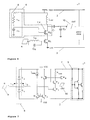
- FIG 1 shows a schematic of a prior art wideband Radio Frequency Low Noise Amplifier (RF LNA) with prior art dual diode ESD protection and a power clamp.
- RF LNA Radio Frequency Low Noise Amplifier
- Figure 2 shows a schematic of a core LNA circuit with an ESD turn-off circuit according to an embodiment
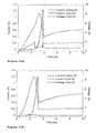
- Figure 3 shows the simulated ESD currents of an ESD protected LNA circuit when subjected to an VDD-to-IN 1 kV HBM ESD stress, with (a) and without (b) an ESD turn-off circuit according to an embodiment.
- Figure 4 shows the measured normalized leakage current after different HBM stress levels for LNAs with and without turn-off circuitry according to an embodiment.
- Figure 5 shows a schematic of the core of a prior art ESD protected LNA.
- Figure 6 shows the LNA of figure 5 with an ESD turn-off circuit according to an embodiment.
- Figure 7 shows a schematic of the core of a prior art ESD protected LNA circuit.
- Figure 8 shows a schematic of the core of the ESD protected LNA circuit of figure 7 with an ESD turn-off circuit according to an embodiment.
- Figure 9 shows a generic schematic of an ESD protected electronic circuit with turn-off circuit according to an embodiment
- Figure 10 is a flow chart illustrating a method for designing an ESD protected electronic circuit with turn-off circuit according to an embodiment.
- top, bottom, over, under and the like in the description and the claims are used for descriptive purposes and not necessarily for describing relative positions. The terms so used are interchangeable under appropriate circumstances and the embodiments of the disclosure described herein can operate in other orientations than described or illustrated herein.
- the effective values of parameters of the selected ESD protection devices are determined in view of the desired ESD protection while the dimensions of these ESD protection devices are also determined in view of their contribution to the circuit performance in normal operation.
- the ESD protected electronic circuit may still fail if the response of an ESD protection device to an ESD event is too slow.
- the ESD protection device may be triggered by an ESD event, it may take some time before the ESD protection device is capable of conveying all unwanted currents towards the power supply lines. These unwanted currents can result from parasitic ESD current paths created by the ESD event between the functional element to be protected by the ESD protection device and the power supply line.
- Radio Frequency Wide Band Low Noise Amplifier RF WB LNA
- the embodiments can be applied to other electronic circuits having ESD protection.
- the thin gate dielectrics used in advanced CMOS technology makes the LNA's RF input very sensitive to ESD stress events. Even with good ESD protection devices, additional precautions need to be taken to prevent gate oxide failure and possible triggering of parasitic ESD current paths during an ESD event. The latter is easily overlooked.
- the LNA is an active feedback, common source amplifier.
- a cascode stage M n1 -M ncas offers gain, while the feedback via the source-follower M n2 and R bal ensures input matching.
- a 30x30 ⁇ m2 multilayer 0.9 nH shunt peaking inductor L load is added in series with the load resistor R load to boost the bandwidth.
- the second stage M nbuf works as a buffer to drive the measurement setup used the measure the performance of the ESD protected circuit.
- the LNA consumes 12.36 mW power with a 1.2 V supply.
- an ESD protection containing two diodes D1, D2 as ESD protection devices for the functional element M n1 and a power clamp between the two power supply lines VDD and VSS is commonly used as a low-capacitance RF ESD protection solution.
- the diodes D1 and D2 are provided between the input terminal IN and respectively the low power supply line VSS and the high power supply line VDD,
- the bandwidth of the RF circuit is traded off with the ESD robustness, i.e. the maximum ESD current that the ESD protection device can convey.
- the input terminal IN is positive biased with respect to the low power supply voltage line VSS IN(positive)-to-VSS(negative) stress
- the high power supply line VDD is positive biased with respect to the input terminal IN VDD(positive)-to-IN(negative).
- All diodes in figure 1 are 40 ⁇ m wide with 50 fF parasitic capacitance and with 3.2 kV Human Body Model robustness.
- An RC triggered NMOS is selected as a power clamp to the LNA circuit.
- the core LNA fails early in the VDD-IN stress combination but also in a VDD-VSS stress combination as a result from triggering of parasitic ESD current paths in the core of the LNA. These parasitic ESD current paths do not occur during normal operation of the ESD protected electronic circuit.
- an alternative methodology to boost the ESD robustness is to keep the parasitic ESD current path off, at least during part of an ESD event, by means of an ESD turn-off circuit.
- a turn-off device 6 in the form of an additional transistor M nTO 7 is added at the drain of M n2 4 inside this parasitic ESD current path.
- the gate of this additional transistor M nTO 7 is connected to an ESD transient RC turn-off timer 8 R TO -C TO , as shown in figure 2 .
- an interrupt circuit 6, shown in figure 2 by the dotted line, comprising a transistor 7 having an RC circuit 8 connected to its gate whereby the resistor connected to the high power supply line VDD 2 is inserted in a parasitic ESD current path.
- the core LNA 1 is shown without the ESD protection devices and the power clamps.
- the gate of M nTO 7 is pulled to VDD 2 via the resistor R TO causing the transistor M nTO 7 to fully conduct. Hence the transistor M nTO 7 does not impact the normal RF circuit operation of the ESD protected LNA circuit 1.
- the additional transistor M nTO 7 is kept off for the initial first nanoseconds of the ESD event, the duration depending on the RC time constant, thereby forcing the corresponding ESD current to flow through the power clamp 5, instead of through the parasitic ESD current path.
- the time constant of the RC circuit 8 R TO -C TO is selected in view of the speed at which the ESD protection device 5 can start conveying the ESD current.
- This response time is a characteristic of the ESD protection device 5 and can to some extent be tuned, e.g. in the case of the DTSCR.
- the time constant is selected to at least turn off a transistor 7 in the parasitic ESD current path until an ESD protection device 5 is triggered to a low-resistance state sufficiently for draining the ESD current to a power supply line 2,3.
- This time constant of the turn-off circuit 8 can be selected such that the parasitic ESD current path is turned during at least a part of the ESD event. However this time constant can be selected to turn off the parasitic ESD current path during the whole duration of the ESD event.
- each of these parasitic ESD current paths a transistor 7 having an RC circuit 8 to its gate can be inserted.
- the RC circuit of the turn-off circuits 8 can be shared to turn off several possible parasitic ESD paths with the same time constant.
- the cascode transistor M ncas is also turned off during stress between VDD and VSS, to prevent failure caused by source-drain filamentation.
- the timer circuit R TO -C TO is also connected to the gate of the cascade transistor.
- Figure 3 shows the simulated voltage and current waveforms during a 1kV Human Body Model VDD-to-IN stress, on the LNA with dual-diode D 1 , D 2 ESD protection and an RC-triggered NMOS as power clamp.
- the ESD current When adding the turn-off circuit 6 with a turn-off device 7 controlled by a timer circuit 8 M nTO -R TO -C TO , the ESD current, normally pushed through the core LNA 4 via parasitic ESD current paths when the power clamp 5 is not yet fully turned on, is reduced from 250mA peak to 20mA peak, preventing early failure of the core LNA 4 at higher ESD stress levels.
- HBM measurements whereby the stress voltage was increased in 250V voltage steps, have been performed on the LNA where a RC-triggered NMOS 5 was used as power clamp, and with the shared turn-off circuit 8 as shown in figure 2 .
- the turn-off timer 8 R TO -C TO was constructed with a 20k ⁇ resistor and a 25pF capacitor, yielding an RC time constant of 500ns. Due to addition of the turn-off circuit 6, the HBM robustness was increased from 2.25kV to 4kV.
- the measured normalized leakage current evolution after each HBM level step is compared in figure 4 for the ESD protected LNA circuit with (open squares) and without (solid diamonds) turn-off circuit 6. Markers are included to indicate the different failure points.
- Table 1 An overview of the HBM measurements on the different circuit variations discussed above for the weakest pin combinations VDD+ to IN- and VDD+ to VSS- is shown in Table 1 below.
- Table 1 Impact of turn-off circuit on On-wafer HBM measurements [kV] time constant Turn-off circuit HBM (kV) HBM (kV) 500ns 200ns 20ns VDD-IN ESD stress VDD-VSS ESD stress - - - 1.5 3 X - - 3.75 6.5 - X - 3.75 - - - X 3.75 -
- the RF design with the turn-off circuitry was tested for system-level ESD stress using an on-wafer Human Metal Model tester which tests the ESD robustness of the system containing the ESD protected circuit. It is important to point out that most RF circuits can not tolerate additional off-chip ESD protection against system level ESD based on a Transient Voltage Suppressor and a current limiting resistor as the associated impedance of this off-chip ESD protection jeopardize the normal operation of the circuit incorporated in the system.
- the LNA design having the turn-off circuit 6 as discussed above could withstand at least 1kV HMM for all possible pin-to-pin combinations even without additional system level ESD protection.
- FIG. 5 shows the core of another ESD protected LNA circuit with cascade configuration.
- the core of this circuit contains a cascode transistor pair M1 and M 2 .
- the gate of transistor M1 is connected to the input terminal IN via an L G -C G parallel circuit providing impedance matching.
- the load capacitor L load determines the resonance peak of this narrow band RF circuit.
- the capacitive divider C 1 -C 2 at the output terminal OUT provides output matching.
- a parasitic ESD current path through the LNA core will be created when the high power supply VDD is stressed with respect to the low power supply VSS (VDD+ VSS-).
- VDD+ VSS- low power supply
- this parasitic ESD current path can be interrupted at least during part of the ESD event by creating a turn-off circuit 6 in this parasitic ESD current path as shown in figure 6 .
- an additional transistor M nTO 7 was inserted in the parasitic ESD current path to allow interrupting this parasitic ESD current path, here an active functional device 4, i.e. transistor M 2 , will be turned off by the RC circuit 8 to interrupt the parasitic ESD current path.
- the turn-off circuit 6 is formed by the transistor M 2 being part of the core of the LNA and operative during normal operation of the LNA and the additional timer circuit 8 R TO -C TO .
- the gate of M 2 is biased to VDD 2 and hence behaves as without the additional R and C. The presence of the turn-off circuit 6 has not impact on the normal operation of the LNA circuit.
- Figure 7 shows the core 4 of another ESD protected LNA circuit 1 with cascade configuration.
- the core of the circuit contains a cascode transistor pair M 1 and M 2 connected to an output buffer M6 which is added to drive the measurement equipment used to the test the performance of the circuit.
- a load resistor R load is added to provide a wide band operation.
- a feedback circuit is provided via the feedback transistor M 3 .
- a current mirror M 4 -M 5 biased via a current source I bias , determines the operation point of this feedback transistor M 3 .
- IN coils L 1 and L 2 are added to compensate for parasitic impedance thereby providing impedance matching.
- Two diodes D 1 and D 2 are connected between the input line and respectively the low power supply line VSS 3 and the high power supply line VDD 2 as ESD protection devices 5 of the active functional device M 1 4.
- a power clamp is connected to the power supply lines VDD 2 and VSS 3.
- a parasitic ESD current path through the LNA core 4 will be created when the high power supply VDD 2 is stressed with respect the input terminal IN 9.
- the feedback transistor M 3 which is connected to the high power supply line VDD via the load resistor R load , will turn on whereby a parasitic ESD current flows in the core of the LNA circuit.
- the gate of the feedback transistor M 3 is an RF point, i.e.
- FIG 8 A solution is shown in figure 8 .
- an additional small transistor M turnoff 7 is inserted in the parasitic ESD current path formed by transistor M 3 during the ESD event.
- the additional transistor 7 is placed in between the drain of the functional transistor M 3 4 and the high power supply line VDD 2, such that the transistor M 3 4 is in between the additional transistor 7 and the RF point.
- a timer circuit 8 R turnoff -C turnoff is connected to the gate of this additional transistor M turnoff 7 .
- the additional transistor M turnoff 7 is dimensioned to have no or minimal impact on the normal operation of the LNA circuit 1.
- the gate of this additional transistor M turnoff 7 is connected via the resistor R turnoff to the high power supply line VDD 2 and the additional transistor M turnoff 7 is switched on such that the current path through transistor M3 is not interrupted.
- a second parasitic ESD current path can be created in case an ESD event occurs whereby the high power supply line VDD 2 is stressed with respect to the low power supply line VSS b3 (VDD+VSS-).
- the transistor M 2 4 can be switched on as its gate is connected to the high power supply line VDD 2 and a parasitic ESD current can flow through the core 4 of the LNA circuit 1.
- this functional transistor M 2 4 can be switched off by a timer circuit 8 at least during part of the ESD event.
- the latter option is shown in figure 8 .
- turn-off circuitry 6 is provided to interrupt parasitic ESD current paths created during an ESD event thereby improving the overall ESD performance of the circuit 1.
- the additional turn-off circuitry 6 prevented parasitic ESD currents path in the core circuit 4 to be triggered during the ESD event.
- These parasitic ESD current paths are current paths that are operative during normal operation of the ESD-protected circuit, but should not conduct current because of an ESD event.
- one or more of the active functional devices 4 of this circuit can however be biased due to the ESD event to the extent that these active functional devices will conduct also during the ESD event.
- a functional device 4 is a device that is also present in the ESD unprotected circuit.
- This functional device 4 can be a passive device such as a coil or resistor. It can also be an active device such as diode or transistor.
- Figure 9 shows as generic schematic of an ESD protected circuit 1 with a turn-off circuitry 6 according to this disclosure.
- the circuit is powered by a high power supply line VDD 2 and a low power supply line VSS 3.
- the circuit 1 has an input terminal IN 9 and an output terminal OUT 10.
- the circuit 1 comprises at least one functional device 4, either passive or active. At least one of these functional devices 4 is protected by one more ESD protection devices 5 configured to bypass during an ESD event the corresponding ESD current to a power supply line.
- a turn-off circuit configured to interrupt, at least during the initial part of the ESD event, this parasitic ESD current path thereby allowing the ESD protection device 5 to be fully triggered by the ESD event.
- This turn-off circuit 6 comprises a turn-off device 7, which can interrupt the parasitic ESD current path, and a timer circuit 8 controlling the operation of this turn-off device 7.
- the turn-off device 7 is a transistor either already present as a functional device or purposively added as turn-off device.
- the timer circuit 8 is an RC delay circuit with the resistor connected to the gate of the transistor used as turn-off device and the power supply.
- Figure 10 is a flow chart illustrating a method for designing an ESD protected circuit 1 having an interrupt or turn-off circuit 6 as disclosed in the foregoing paragraphs and illustrated in figure 9 .
- the method comprises providing an ESD protected circuit 1, determining in this ESD protected circuit 1 at least one parasitic current path and creating in this at least one parasitic current path an interrupt circuit 6.
Landscapes
- Semiconductor Integrated Circuits (AREA)
- Metal-Oxide And Bipolar Metal-Oxide Semiconductor Integrated Circuits (AREA)
- Design And Manufacture Of Integrated Circuits (AREA)
- Amplifiers (AREA)
Applications Claiming Priority (1)
| Application Number | Priority Date | Filing Date | Title |
|---|---|---|---|
| US23754509P | 2009-08-27 | 2009-08-27 |
Publications (1)
| Publication Number | Publication Date |
|---|---|
| EP2293331A1 true EP2293331A1 (de) | 2011-03-09 |
Family
ID=43033224
Family Applications (1)
| Application Number | Title | Priority Date | Filing Date |
|---|---|---|---|
| EP10075362A Ceased EP2293331A1 (de) | 2009-08-27 | 2010-08-23 | Verfahren für den Entwurf von integrierten elektronischen Schaltungen mit Schutz vor elektrostatischer Entladung und damit erhaltene Schaltungen |
Country Status (3)
| Country | Link |
|---|---|
| US (1) | US20110051301A1 (de) |
| EP (1) | EP2293331A1 (de) |
| JP (1) | JP2011071502A (de) |
Families Citing this family (10)
| Publication number | Priority date | Publication date | Assignee | Title |
|---|---|---|---|---|
| US8181140B2 (en) * | 2009-11-09 | 2012-05-15 | Xilinx, Inc. | T-coil network design for improved bandwidth and electrostatic discharge immunity |
| JP5743850B2 (ja) * | 2011-10-28 | 2015-07-01 | 株式会社東芝 | 集積回路 |
| TWI492540B (zh) * | 2012-07-02 | 2015-07-11 | Nuvoton Technology Corp | 熔絲電路 |
| US9106072B2 (en) * | 2012-12-19 | 2015-08-11 | Qualcomm Incorporated | Electrostatic discharge protection of amplifier cascode devices |
| US9929698B2 (en) | 2013-03-15 | 2018-03-27 | Qualcomm Incorporated | Radio frequency integrated circuit (RFIC) charged-device model (CDM) protection |
| JP2014241537A (ja) | 2013-06-12 | 2014-12-25 | 株式会社東芝 | 静電気保護回路 |
| US9473085B2 (en) * | 2014-09-09 | 2016-10-18 | Qualcomm Incorporated | Input switch leakage compensation |
| US10325906B2 (en) * | 2016-09-23 | 2019-06-18 | Taiwan Semiconductor Manufacturing Company, Ltd. | ESD testing structure, method of using same and method of forming same |
| US11462904B2 (en) * | 2021-01-20 | 2022-10-04 | Hangzhou Geo-Chip Technology Co., Ltd. | Apparatus for protection against electrostatic discharge and method of manufacturing the same |
| JP2023134064A (ja) | 2022-03-14 | 2023-09-27 | キオクシア株式会社 | 半導体装置、及び、半導体装置の製造方法 |
Citations (7)
| Publication number | Priority date | Publication date | Assignee | Title |
|---|---|---|---|---|
| US6249410B1 (en) * | 1999-08-23 | 2001-06-19 | Taiwan Semiconductor Manufacturing Company | ESD protection circuit without overstress gate-driven effect |
| WO2002029950A2 (en) * | 2000-10-06 | 2002-04-11 | Qualcomm Incorporated | Electro-static discharge protection circuit |
| US20030223166A1 (en) * | 2002-05-29 | 2003-12-04 | Zi-Ping Chen | ESD protection circuit with whole-chip ESD protection |
| US20050135033A1 (en) * | 2003-12-22 | 2005-06-23 | Nobutaka Kitagawa | Semiconductor integrated circuit apparatus |
| FR2877512A1 (fr) * | 2004-11-02 | 2006-05-05 | Ind Tech Res Inst | Protection contre les decharges electrostatiques pour amplificateur de puissance dans un circuit integre a radiofrequence |
| US20070182444A1 (en) * | 2006-01-24 | 2007-08-09 | Nec Electronics Corporation | Semiconductor integrated circuit device |
| EP2037501A1 (de) | 2007-09-14 | 2009-03-18 | Interuniversitair Microelektronica Centrum Vzw | Schnellauslösendes ESD-Schutzgerät und Konstruktionsverfahren dafür |
-
2010
- 2010-08-23 EP EP10075362A patent/EP2293331A1/de not_active Ceased
- 2010-08-25 JP JP2010188287A patent/JP2011071502A/ja not_active Withdrawn
- 2010-08-26 US US12/869,318 patent/US20110051301A1/en not_active Abandoned
Patent Citations (7)
| Publication number | Priority date | Publication date | Assignee | Title |
|---|---|---|---|---|
| US6249410B1 (en) * | 1999-08-23 | 2001-06-19 | Taiwan Semiconductor Manufacturing Company | ESD protection circuit without overstress gate-driven effect |
| WO2002029950A2 (en) * | 2000-10-06 | 2002-04-11 | Qualcomm Incorporated | Electro-static discharge protection circuit |
| US20030223166A1 (en) * | 2002-05-29 | 2003-12-04 | Zi-Ping Chen | ESD protection circuit with whole-chip ESD protection |
| US20050135033A1 (en) * | 2003-12-22 | 2005-06-23 | Nobutaka Kitagawa | Semiconductor integrated circuit apparatus |
| FR2877512A1 (fr) * | 2004-11-02 | 2006-05-05 | Ind Tech Res Inst | Protection contre les decharges electrostatiques pour amplificateur de puissance dans un circuit integre a radiofrequence |
| US20070182444A1 (en) * | 2006-01-24 | 2007-08-09 | Nec Electronics Corporation | Semiconductor integrated circuit device |
| EP2037501A1 (de) | 2007-09-14 | 2009-03-18 | Interuniversitair Microelektronica Centrum Vzw | Schnellauslösendes ESD-Schutzgerät und Konstruktionsverfahren dafür |
Also Published As
| Publication number | Publication date |
|---|---|
| JP2011071502A (ja) | 2011-04-07 |
| US20110051301A1 (en) | 2011-03-03 |
Similar Documents
| Publication | Publication Date | Title |
|---|---|---|
| EP2293331A1 (de) | Verfahren für den Entwurf von integrierten elektronischen Schaltungen mit Schutz vor elektrostatischer Entladung und damit erhaltene Schaltungen | |
| TWI460847B (zh) | 多電壓靜電放電防護 | |
| US5781388A (en) | Non-breakdown triggered electrostatic discharge protection circuit for an integrated circuit and method therefor | |
| US8525265B2 (en) | Electrostatic discharge protection circuit | |
| EP0583105A1 (de) | ESD-Schutz mittels eines bipolaren NPN-Transistors | |
| US20170155243A1 (en) | Electrostatic discharge (esd) clamp on-time control | |
| EP2037501A1 (de) | Schnellauslösendes ESD-Schutzgerät und Konstruktionsverfahren dafür | |
| US6927957B1 (en) | Electrostatic discharge clamp | |
| US8508893B2 (en) | Method for providing wideband electrostatic discharge protection and circuits obtained therewith | |
| US12063014B2 (en) | Amplifier having electrostatic discharge and surge protection circuit | |
| CN100508322C (zh) | 用于集成电路器件的保护电路 | |
| WO2012125179A1 (en) | Input-output esd protection | |
| US10181721B2 (en) | Area-efficient active-FET ESD protection circuit | |
| US6801417B2 (en) | Semiconductor integrated circuit device | |
| US20200091136A1 (en) | Rc-triggered bracing circuit | |
| CN101383507A (zh) | 一种静电放电防护电路 | |
| US8824111B2 (en) | Electrostatic discharge protection | |
| KR20110042115A (ko) | 멀티-다이 패키지에서 과전압 보호를 위한 시스템 및 방법 | |
| Linten et al. | A 4.5 kv hbm, 300 v cdm, 1.2 kv hmm esd protected dc-to-16.1 ghz wideband lna in 90 nm cmos | |
| US7876541B2 (en) | Electrostatic discharge protection circuit and electrostatic discharge protection method of a semiconductor memory device | |
| US7292421B2 (en) | Local ESD power rail clamp which implements switchable I/O decoupling capacitance function | |
| CN118889351A (zh) | 准静态esd箝位电路 | |
| US6633468B1 (en) | High voltage protection circuit for improved oxide reliability | |
| Huang et al. | A High Voltage Tolerant Supply Clamp for ESD Protection in a 45-nm SOI Technology | |
| Muthukrishnan et al. | A novel on-chip protection circuit for RFICs implemented in D-mode pHEMT technology |
Legal Events
| Date | Code | Title | Description |
|---|---|---|---|
| PUAI | Public reference made under article 153(3) epc to a published international application that has entered the european phase |
Free format text: ORIGINAL CODE: 0009012 |
|
| AK | Designated contracting states |
Kind code of ref document: A1 Designated state(s): AL AT BE BG CH CY CZ DE DK EE ES FI FR GB GR HR HU IE IS IT LI LT LU LV MC MK MT NL NO PL PT RO SE SI SK SM TR |
|
| AX | Request for extension of the european patent |
Extension state: BA ME RS |
|
| 17P | Request for examination filed |
Effective date: 20110824 |
|
| 17Q | First examination report despatched |
Effective date: 20111228 |
|
| STAA | Information on the status of an ep patent application or granted ep patent |
Free format text: STATUS: THE APPLICATION HAS BEEN REFUSED |
|
| 18R | Application refused |
Effective date: 20130221 |