EP2293324A1 - Packaging structure and method for manufacturing packaging structure - Google Patents
Packaging structure and method for manufacturing packaging structure Download PDFInfo
- Publication number
- EP2293324A1 EP2293324A1 EP09769870A EP09769870A EP2293324A1 EP 2293324 A1 EP2293324 A1 EP 2293324A1 EP 09769870 A EP09769870 A EP 09769870A EP 09769870 A EP09769870 A EP 09769870A EP 2293324 A1 EP2293324 A1 EP 2293324A1
- Authority
- EP
- European Patent Office
- Prior art keywords
- mounting structure
- electronic component
- paste material
- electrode
- substrate
- Prior art date
- Legal status (The legal status is an assumption and is not a legal conclusion. Google has not performed a legal analysis and makes no representation as to the accuracy of the status listed.)
- Granted
Links
Images






Classifications
-
- H—ELECTRICITY
- H10—SEMICONDUCTOR DEVICES; ELECTRIC SOLID-STATE DEVICES NOT OTHERWISE PROVIDED FOR
- H10H—INORGANIC LIGHT-EMITTING SEMICONDUCTOR DEVICES HAVING POTENTIAL BARRIERS
- H10H20/00—Individual inorganic light-emitting semiconductor devices having potential barriers, e.g. light-emitting diodes [LED]
- H10H20/80—Constructional details
- H10H20/85—Packages
- H10H20/857—Interconnections, e.g. lead-frames, bond wires or solder balls
-
- B—PERFORMING OPERATIONS; TRANSPORTING
- B23—MACHINE TOOLS; METAL-WORKING NOT OTHERWISE PROVIDED FOR
- B23K—SOLDERING OR UNSOLDERING; WELDING; CLADDING OR PLATING BY SOLDERING OR WELDING; CUTTING BY APPLYING HEAT LOCALLY, e.g. FLAME CUTTING; WORKING BY LASER BEAM
- B23K1/00—Soldering, e.g. brazing, or unsoldering
- B23K1/0008—Soldering, e.g. brazing, or unsoldering specially adapted for particular articles or work
- B23K1/0016—Soldering of electronic components
-
- B—PERFORMING OPERATIONS; TRANSPORTING
- B23—MACHINE TOOLS; METAL-WORKING NOT OTHERWISE PROVIDED FOR
- B23K—SOLDERING OR UNSOLDERING; WELDING; CLADDING OR PLATING BY SOLDERING OR WELDING; CUTTING BY APPLYING HEAT LOCALLY, e.g. FLAME CUTTING; WORKING BY LASER BEAM
- B23K35/00—Rods, electrodes, materials, or media, for use in soldering, welding, or cutting
- B23K35/02—Rods, electrodes, materials, or media, for use in soldering, welding, or cutting characterised by mechanical features, e.g. shape
- B23K35/0222—Rods, electrodes, materials, or media, for use in soldering, welding, or cutting characterised by mechanical features, e.g. shape for use in soldering or brazing
- B23K35/0244—Powders, particles or spheres; Preforms made therefrom
-
- B—PERFORMING OPERATIONS; TRANSPORTING
- B23—MACHINE TOOLS; METAL-WORKING NOT OTHERWISE PROVIDED FOR
- B23K—SOLDERING OR UNSOLDERING; WELDING; CLADDING OR PLATING BY SOLDERING OR WELDING; CUTTING BY APPLYING HEAT LOCALLY, e.g. FLAME CUTTING; WORKING BY LASER BEAM
- B23K35/00—Rods, electrodes, materials, or media, for use in soldering, welding, or cutting
- B23K35/02—Rods, electrodes, materials, or media, for use in soldering, welding, or cutting characterised by mechanical features, e.g. shape
- B23K35/0222—Rods, electrodes, materials, or media, for use in soldering, welding, or cutting characterised by mechanical features, e.g. shape for use in soldering or brazing
- B23K35/0244—Powders, particles or spheres; Preforms made therefrom
- B23K35/025—Pastes, creams or slurries
-
- H—ELECTRICITY
- H05—ELECTRIC TECHNIQUES NOT OTHERWISE PROVIDED FOR
- H05K—PRINTED CIRCUITS; CASINGS OR CONSTRUCTIONAL DETAILS OF ELECTRIC APPARATUS; MANUFACTURE OF ASSEMBLAGES OF ELECTRICAL COMPONENTS
- H05K3/00—Apparatus or processes for manufacturing printed circuits
- H05K3/30—Assembling printed circuits with electric components, e.g. with resistors
- H05K3/32—Assembling printed circuits with electric components, e.g. with resistors electrically connecting electric components or wires to printed circuits
- H05K3/321—Assembling printed circuits with electric components, e.g. with resistors electrically connecting electric components or wires to printed circuits by conductive adhesives
-
- H—ELECTRICITY
- H10—SEMICONDUCTOR DEVICES; ELECTRIC SOLID-STATE DEVICES NOT OTHERWISE PROVIDED FOR
- H10H—INORGANIC LIGHT-EMITTING SEMICONDUCTOR DEVICES HAVING POTENTIAL BARRIERS
- H10H20/00—Individual inorganic light-emitting semiconductor devices having potential barriers, e.g. light-emitting diodes [LED]
- H10H20/80—Constructional details
- H10H20/85—Packages
- H10H20/858—Means for heat extraction or cooling
- H10H20/8581—Means for heat extraction or cooling characterised by their material
-
- H—ELECTRICITY
- H05—ELECTRIC TECHNIQUES NOT OTHERWISE PROVIDED FOR
- H05K—PRINTED CIRCUITS; CASINGS OR CONSTRUCTIONAL DETAILS OF ELECTRIC APPARATUS; MANUFACTURE OF ASSEMBLAGES OF ELECTRICAL COMPONENTS
- H05K2201/00—Indexing scheme relating to printed circuits covered by H05K1/00
- H05K2201/03—Conductive materials
- H05K2201/0332—Structure of the conductor
- H05K2201/0364—Conductor shape
- H05K2201/0367—Metallic bump or raised conductor not used as solder bump
-
- H—ELECTRICITY
- H05—ELECTRIC TECHNIQUES NOT OTHERWISE PROVIDED FOR
- H05K—PRINTED CIRCUITS; CASINGS OR CONSTRUCTIONAL DETAILS OF ELECTRIC APPARATUS; MANUFACTURE OF ASSEMBLAGES OF ELECTRICAL COMPONENTS
- H05K2201/00—Indexing scheme relating to printed circuits covered by H05K1/00
- H05K2201/10—Details of components or other objects attached to or integrated in a printed circuit board
- H05K2201/10007—Types of components
- H05K2201/10106—Light emitting diode [LED]
-
- H—ELECTRICITY
- H05—ELECTRIC TECHNIQUES NOT OTHERWISE PROVIDED FOR
- H05K—PRINTED CIRCUITS; CASINGS OR CONSTRUCTIONAL DETAILS OF ELECTRIC APPARATUS; MANUFACTURE OF ASSEMBLAGES OF ELECTRICAL COMPONENTS
- H05K2201/00—Indexing scheme relating to printed circuits covered by H05K1/00
- H05K2201/10—Details of components or other objects attached to or integrated in a printed circuit board
- H05K2201/10007—Types of components
- H05K2201/10166—Transistor
-
- H—ELECTRICITY
- H05—ELECTRIC TECHNIQUES NOT OTHERWISE PROVIDED FOR
- H05K—PRINTED CIRCUITS; CASINGS OR CONSTRUCTIONAL DETAILS OF ELECTRIC APPARATUS; MANUFACTURE OF ASSEMBLAGES OF ELECTRICAL COMPONENTS
- H05K2201/00—Indexing scheme relating to printed circuits covered by H05K1/00
- H05K2201/20—Details of printed circuits not provided for in H05K2201/01 - H05K2201/10
- H05K2201/2036—Permanent spacer or stand-off in a printed circuit or printed circuit assembly
-
- H—ELECTRICITY
- H05—ELECTRIC TECHNIQUES NOT OTHERWISE PROVIDED FOR
- H05K—PRINTED CIRCUITS; CASINGS OR CONSTRUCTIONAL DETAILS OF ELECTRIC APPARATUS; MANUFACTURE OF ASSEMBLAGES OF ELECTRICAL COMPONENTS
- H05K2203/00—Indexing scheme relating to apparatus or processes for manufacturing printed circuits covered by H05K3/00
- H05K2203/11—Treatments characterised by their effect, e.g. heating, cooling, roughening
- H05K2203/1131—Sintering, i.e. fusing of metal particles to achieve or improve electrical conductivity
-
- H—ELECTRICITY
- H05—ELECTRIC TECHNIQUES NOT OTHERWISE PROVIDED FOR
- H05K—PRINTED CIRCUITS; CASINGS OR CONSTRUCTIONAL DETAILS OF ELECTRIC APPARATUS; MANUFACTURE OF ASSEMBLAGES OF ELECTRICAL COMPONENTS
- H05K2203/00—Indexing scheme relating to apparatus or processes for manufacturing printed circuits covered by H05K3/00
- H05K2203/11—Treatments characterised by their effect, e.g. heating, cooling, roughening
- H05K2203/1178—Means for venting or for letting gases escape
-
- H—ELECTRICITY
- H05—ELECTRIC TECHNIQUES NOT OTHERWISE PROVIDED FOR
- H05K—PRINTED CIRCUITS; CASINGS OR CONSTRUCTIONAL DETAILS OF ELECTRIC APPARATUS; MANUFACTURE OF ASSEMBLAGES OF ELECTRICAL COMPONENTS
- H05K3/00—Apparatus or processes for manufacturing printed circuits
- H05K3/40—Forming printed elements for providing electric connections to or between printed circuits
- H05K3/4007—Surface contacts, e.g. bumps
-
- H—ELECTRICITY
- H10—SEMICONDUCTOR DEVICES; ELECTRIC SOLID-STATE DEVICES NOT OTHERWISE PROVIDED FOR
- H10F—INORGANIC SEMICONDUCTOR DEVICES SENSITIVE TO INFRARED RADIATION, LIGHT, ELECTROMAGNETIC RADIATION OF SHORTER WAVELENGTH OR CORPUSCULAR RADIATION
- H10F77/00—Constructional details of devices covered by this subclass
- H10F77/60—Arrangements for cooling, heating, ventilating or compensating for temperature fluctuations
-
- H—ELECTRICITY
- H10—SEMICONDUCTOR DEVICES; ELECTRIC SOLID-STATE DEVICES NOT OTHERWISE PROVIDED FOR
- H10H—INORGANIC LIGHT-EMITTING SEMICONDUCTOR DEVICES HAVING POTENTIAL BARRIERS
- H10H20/00—Individual inorganic light-emitting semiconductor devices having potential barriers, e.g. light-emitting diodes [LED]
- H10H20/80—Constructional details
- H10H20/85—Packages
- H10H20/858—Means for heat extraction or cooling
- H10H20/8585—Means for heat extraction or cooling being an interconnection
-
- H—ELECTRICITY
- H10—SEMICONDUCTOR DEVICES; ELECTRIC SOLID-STATE DEVICES NOT OTHERWISE PROVIDED FOR
- H10W—GENERIC PACKAGES, INTERCONNECTIONS, CONNECTORS OR OTHER CONSTRUCTIONAL DETAILS OF DEVICES COVERED BY CLASS H10
- H10W72/00—Interconnections or connectors in packages
- H10W72/071—Connecting or disconnecting
- H10W72/073—Connecting or disconnecting of die-attach connectors
-
- H—ELECTRICITY
- H10—SEMICONDUCTOR DEVICES; ELECTRIC SOLID-STATE DEVICES NOT OTHERWISE PROVIDED FOR
- H10W—GENERIC PACKAGES, INTERCONNECTIONS, CONNECTORS OR OTHER CONSTRUCTIONAL DETAILS OF DEVICES COVERED BY CLASS H10
- H10W72/00—Interconnections or connectors in packages
- H10W72/071—Connecting or disconnecting
- H10W72/073—Connecting or disconnecting of die-attach connectors
- H10W72/07321—Aligning
- H10W72/07327—Aligning involving guiding structures, e.g. spacers or supporting members
-
- H—ELECTRICITY
- H10—SEMICONDUCTOR DEVICES; ELECTRIC SOLID-STATE DEVICES NOT OTHERWISE PROVIDED FOR
- H10W—GENERIC PACKAGES, INTERCONNECTIONS, CONNECTORS OR OTHER CONSTRUCTIONAL DETAILS OF DEVICES COVERED BY CLASS H10
- H10W72/00—Interconnections or connectors in packages
- H10W72/071—Connecting or disconnecting
- H10W72/073—Connecting or disconnecting of die-attach connectors
- H10W72/07331—Connecting techniques
-
- H—ELECTRICITY
- H10—SEMICONDUCTOR DEVICES; ELECTRIC SOLID-STATE DEVICES NOT OTHERWISE PROVIDED FOR
- H10W—GENERIC PACKAGES, INTERCONNECTIONS, CONNECTORS OR OTHER CONSTRUCTIONAL DETAILS OF DEVICES COVERED BY CLASS H10
- H10W72/00—Interconnections or connectors in packages
- H10W72/071—Connecting or disconnecting
- H10W72/073—Connecting or disconnecting of die-attach connectors
- H10W72/07331—Connecting techniques
- H10W72/07332—Compression bonding, e.g. thermocompression bonding
- H10W72/07333—Ultrasonic bonding, e.g. thermosonic bonding
-
- H—ELECTRICITY
- H10—SEMICONDUCTOR DEVICES; ELECTRIC SOLID-STATE DEVICES NOT OTHERWISE PROVIDED FOR
- H10W—GENERIC PACKAGES, INTERCONNECTIONS, CONNECTORS OR OTHER CONSTRUCTIONAL DETAILS OF DEVICES COVERED BY CLASS H10
- H10W72/00—Interconnections or connectors in packages
- H10W72/071—Connecting or disconnecting
- H10W72/074—Connecting or disconnecting of anisotropic conductive adhesives
-
- H—ELECTRICITY
- H10—SEMICONDUCTOR DEVICES; ELECTRIC SOLID-STATE DEVICES NOT OTHERWISE PROVIDED FOR
- H10W—GENERIC PACKAGES, INTERCONNECTIONS, CONNECTORS OR OTHER CONSTRUCTIONAL DETAILS OF DEVICES COVERED BY CLASS H10
- H10W72/00—Interconnections or connectors in packages
- H10W72/20—Bump connectors, e.g. solder bumps or copper pillars; Dummy bumps; Thermal bumps
- H10W72/29—Bond pads specially adapted therefor
-
- H—ELECTRICITY
- H10—SEMICONDUCTOR DEVICES; ELECTRIC SOLID-STATE DEVICES NOT OTHERWISE PROVIDED FOR
- H10W—GENERIC PACKAGES, INTERCONNECTIONS, CONNECTORS OR OTHER CONSTRUCTIONAL DETAILS OF DEVICES COVERED BY CLASS H10
- H10W72/00—Interconnections or connectors in packages
- H10W72/30—Die-attach connectors
- H10W72/321—Structures or relative sizes of die-attach connectors
-
- H—ELECTRICITY
- H10—SEMICONDUCTOR DEVICES; ELECTRIC SOLID-STATE DEVICES NOT OTHERWISE PROVIDED FOR
- H10W—GENERIC PACKAGES, INTERCONNECTIONS, CONNECTORS OR OTHER CONSTRUCTIONAL DETAILS OF DEVICES COVERED BY CLASS H10
- H10W72/00—Interconnections or connectors in packages
- H10W72/30—Die-attach connectors
- H10W72/321—Structures or relative sizes of die-attach connectors
- H10W72/325—Die-attach connectors having a filler embedded in a matrix
-
- H—ELECTRICITY
- H10—SEMICONDUCTOR DEVICES; ELECTRIC SOLID-STATE DEVICES NOT OTHERWISE PROVIDED FOR
- H10W—GENERIC PACKAGES, INTERCONNECTIONS, CONNECTORS OR OTHER CONSTRUCTIONAL DETAILS OF DEVICES COVERED BY CLASS H10
- H10W72/00—Interconnections or connectors in packages
- H10W72/30—Die-attach connectors
- H10W72/351—Materials of die-attach connectors
- H10W72/352—Materials of die-attach connectors comprising metals or metalloids, e.g. solders
-
- H—ELECTRICITY
- H10—SEMICONDUCTOR DEVICES; ELECTRIC SOLID-STATE DEVICES NOT OTHERWISE PROVIDED FOR
- H10W—GENERIC PACKAGES, INTERCONNECTIONS, CONNECTORS OR OTHER CONSTRUCTIONAL DETAILS OF DEVICES COVERED BY CLASS H10
- H10W72/00—Interconnections or connectors in packages
- H10W72/30—Die-attach connectors
- H10W72/351—Materials of die-attach connectors
- H10W72/353—Materials of die-attach connectors not comprising solid metals or solid metalloids, e.g. ceramics
- H10W72/354—Materials of die-attach connectors not comprising solid metals or solid metalloids, e.g. ceramics comprising polymers
-
- H—ELECTRICITY
- H10—SEMICONDUCTOR DEVICES; ELECTRIC SOLID-STATE DEVICES NOT OTHERWISE PROVIDED FOR
- H10W—GENERIC PACKAGES, INTERCONNECTIONS, CONNECTORS OR OTHER CONSTRUCTIONAL DETAILS OF DEVICES COVERED BY CLASS H10
- H10W72/00—Interconnections or connectors in packages
- H10W72/851—Dispositions of multiple connectors or interconnections
- H10W72/874—On different surfaces
- H10W72/884—Die-attach connectors and bond wires
-
- H—ELECTRICITY
- H10—SEMICONDUCTOR DEVICES; ELECTRIC SOLID-STATE DEVICES NOT OTHERWISE PROVIDED FOR
- H10W—GENERIC PACKAGES, INTERCONNECTIONS, CONNECTORS OR OTHER CONSTRUCTIONAL DETAILS OF DEVICES COVERED BY CLASS H10
- H10W72/00—Interconnections or connectors in packages
- H10W72/90—Bond pads, in general
- H10W72/921—Structures or relative sizes of bond pads
- H10W72/926—Multiple bond pads having different sizes
-
- H—ELECTRICITY
- H10—SEMICONDUCTOR DEVICES; ELECTRIC SOLID-STATE DEVICES NOT OTHERWISE PROVIDED FOR
- H10W—GENERIC PACKAGES, INTERCONNECTIONS, CONNECTORS OR OTHER CONSTRUCTIONAL DETAILS OF DEVICES COVERED BY CLASS H10
- H10W72/00—Interconnections or connectors in packages
- H10W72/90—Bond pads, in general
- H10W72/931—Shapes of bond pads
-
- H—ELECTRICITY
- H10—SEMICONDUCTOR DEVICES; ELECTRIC SOLID-STATE DEVICES NOT OTHERWISE PROVIDED FOR
- H10W—GENERIC PACKAGES, INTERCONNECTIONS, CONNECTORS OR OTHER CONSTRUCTIONAL DETAILS OF DEVICES COVERED BY CLASS H10
- H10W72/00—Interconnections or connectors in packages
- H10W72/90—Bond pads, in general
- H10W72/941—Dispositions of bond pads
- H10W72/944—Dispositions of multiple bond pads
-
- H—ELECTRICITY
- H10—SEMICONDUCTOR DEVICES; ELECTRIC SOLID-STATE DEVICES NOT OTHERWISE PROVIDED FOR
- H10W—GENERIC PACKAGES, INTERCONNECTIONS, CONNECTORS OR OTHER CONSTRUCTIONAL DETAILS OF DEVICES COVERED BY CLASS H10
- H10W74/00—Encapsulations, e.g. protective coatings
- H10W74/01—Manufacture or treatment
- H10W74/012—Manufacture or treatment of encapsulations on active surfaces of flip-chip devices, e.g. forming underfills
-
- H—ELECTRICITY
- H10—SEMICONDUCTOR DEVICES; ELECTRIC SOLID-STATE DEVICES NOT OTHERWISE PROVIDED FOR
- H10W—GENERIC PACKAGES, INTERCONNECTIONS, CONNECTORS OR OTHER CONSTRUCTIONAL DETAILS OF DEVICES COVERED BY CLASS H10
- H10W74/00—Encapsulations, e.g. protective coatings
- H10W74/10—Encapsulations, e.g. protective coatings characterised by their shape or disposition
- H10W74/15—Encapsulations, e.g. protective coatings characterised by their shape or disposition on active surfaces of flip-chip devices, e.g. underfills
-
- H—ELECTRICITY
- H10—SEMICONDUCTOR DEVICES; ELECTRIC SOLID-STATE DEVICES NOT OTHERWISE PROVIDED FOR
- H10W—GENERIC PACKAGES, INTERCONNECTIONS, CONNECTORS OR OTHER CONSTRUCTIONAL DETAILS OF DEVICES COVERED BY CLASS H10
- H10W90/00—Package configurations
- H10W90/701—Package configurations characterised by the relative positions of pads or connectors relative to package parts
- H10W90/721—Package configurations characterised by the relative positions of pads or connectors relative to package parts of bump connectors
- H10W90/724—Package configurations characterised by the relative positions of pads or connectors relative to package parts of bump connectors between a chip and a stacked insulating package substrate, interposer or RDL
-
- H—ELECTRICITY
- H10—SEMICONDUCTOR DEVICES; ELECTRIC SOLID-STATE DEVICES NOT OTHERWISE PROVIDED FOR
- H10W—GENERIC PACKAGES, INTERCONNECTIONS, CONNECTORS OR OTHER CONSTRUCTIONAL DETAILS OF DEVICES COVERED BY CLASS H10
- H10W90/00—Package configurations
- H10W90/701—Package configurations characterised by the relative positions of pads or connectors relative to package parts
- H10W90/731—Package configurations characterised by the relative positions of pads or connectors relative to package parts of die-attach connectors
- H10W90/734—Package configurations characterised by the relative positions of pads or connectors relative to package parts of die-attach connectors between a chip and a stacked insulating package substrate, interposer or RDL
-
- H—ELECTRICITY
- H10—SEMICONDUCTOR DEVICES; ELECTRIC SOLID-STATE DEVICES NOT OTHERWISE PROVIDED FOR
- H10W—GENERIC PACKAGES, INTERCONNECTIONS, CONNECTORS OR OTHER CONSTRUCTIONAL DETAILS OF DEVICES COVERED BY CLASS H10
- H10W90/00—Package configurations
- H10W90/701—Package configurations characterised by the relative positions of pads or connectors relative to package parts
- H10W90/751—Package configurations characterised by the relative positions of pads or connectors relative to package parts of bond wires
- H10W90/754—Package configurations characterised by the relative positions of pads or connectors relative to package parts of bond wires between a chip and a stacked insulating package substrate, interposer or RDL
Definitions
- the present invention relates to a mounting structure and a method of manufacturing the mounting structure.
- metal nanoparticles refers to metal particles of a size with a mean particle diameter that is less than 50 nm, such as Au, Ag, or Cu (hereunder, referred to as “metal nanoparticles”). Since the surface activity of such metal nanoparticles is high compared to a bulk material as the result of miniaturization, bonding is possible at a low temperature, and a high fusing point that is equivalent to a bulk material is obtained when bonding occurs and the size increases.
- Figure 16(a), Figure 17(a) , and Figure 18(a) are plan views that illustrate a substrate during a mounting step.
- Figure 16(b), Figure 17(b) , and Figure 18(b) are cross-sectional views that represent a section along a line GG' in Figure 16(a), Figure 17(a) , and Figure 18(a), respectively.
- a substrate 1001 is prepared in which conductor wiring 1002 is formed on a base material.
- a bonding material portion 1013 is formed at component mounting positions on the conductor wiring 1002 using a paste material that includes metal nanoparticles (hereunder, referred to as "metal nanoparticle paste material").
- electrodes 1014 of an electronic component 1003 are positioned facing the bonding material portion 1013, and the electronic component 1003 is mounted on the substrate 1001. Further, by applying energy such as heat to the bonding material portion 1013, the bonding material portion 1013 is bonded and cured to form joints 1015, and thereby bond the electrodes 1014 of the electronic component 1003 and the conductor wiring 1002 of the substrate 1001. As a result, as shown in Figures 18(a) and (b), a mounting structure is produced in which the electrodes 1014 of the electronic component 1003, the joints 1015, and the conductor wiring 1002 are connected in that order in a layered structure.
- the metal nanoparticle paste material is stabilized by means of a dispersing agent to prevent polymerization of the metal nanoparticles.
- a dispersing agent to prevent polymerization of the metal nanoparticles.
- Patent Document 1 A method has been proposed that uses this kind of metal nanoparticle paste material when mounting an LED as an electronic component (for example, see Patent Document 1).
- a metal nanoparticle paste is cured by applying ultrasonic vibrations thereto.
- ultrasonic vibrations when using ultrasonic vibrations, in some cases damage is caused to the electronic components or the bonding is insufficient.
- a method has also been proposed in which curing is performed by heating in the same way as described above together with the use of ultrasonic vibrations or instead of using ultrasonic vibrations.
- Patent Document 1 Japanese Patent Laid-Open No. 2005-136399
- Figures 19(a) to (f) are views that illustrate a method of manufacturing a mounting structure 100 when mounting an LED as an electronic component.
- the substrate electrodes include an electrode 2a and an electrode 2b of different sizes.
- a metal nanoparticle paste material is coated on the electrodes 2a and 2b, to form bonding material portions 13a and 13b.
- the electronic component 3 that is an LED has electrodes 21 a and 21 b that correspond to the electrodes 2a and 2b of a substrate 1.
- a face of the electronic component 3 on a side opposite the side on which the electrodes 21 a and 21 b are formed is held by suction by a mounting tool 16, and the electronic component 3 is placed on the bonding material portions 13a and 13b ( Figure 19(d) ).
- drying and a heat treatment is performed, so that the metal nanoparticle paste material of the bonding material portions 13a and 13b cures to form joints 15a and 15b, and thereby produce the mounting structure 100 ( Figure 19(e) ).
- the electrodes 2a and 21a of the LED are a size of an area of several mm square, as shown in the enlarged view of the bonding material portion 13a shown in Figure 19(f) , a peripheral portion 13e of the bonding material portion 13a is cured first, and thereafter the central portion is cured. Consequently, it is difficult to let a gas 22 that arises in the vicinity of the central portion escape to outside of the bonding material portion 13a. As a result, the gas is liable to remain inside the joint 15 after the heat treatment, and a bonding failure may occur.
- the bonding material portion 13a is made with a thin thickness, the area of a portion at which gas generated at the central portion escapes decreases. Consequently, the gas is more liable to remain after the heat treatment.
- the present invention has been made in view of the problems associated with the conventional mounting structure, and an object of the invention is to provide a mounting structure that can efficiently allow gaseous matter that is generated when performing a heat treatment to escape to outside, as well as a method of manufacturing the mounting structure.
- the 1 st aspect of the present invention is a mounting structure, comprising:
- the 2 nd aspect of the present invention is the mounting structure according to the 1 st aspect of the present invention, wherein the member is embedded at a central portion of the joint, and is made of a material with a higher thermal conductivity than the metal nanoparticle paste material.
- the 3 rd aspect of the present invention is the mounting structure according to the 1 st aspect of the present invention, wherein the member is a member which is embedded at a central portion of the joint, and which has supplied oxygen to the metal nanoparticle paste material.
- the 4 th aspect of the present invention is the mounting structure according to any of the 1 st to 3r d aspects of the present invention, wherein:
- the 5 th aspect of the present invention is the mounting structure according to the 4 th aspect of the present invention, wherein the member is formed by unevenness on a surface of the electrode of the substrate or the electrode of the electronic component.
- the 6 th aspect of the present invention is the mounting structure according to the 1 st aspect of the present invention, wherein the joint has a heat radiation function.
- the 7 th aspect of the present invention is the mounting structure according to any of the 1 st to 3 rd aspects of the present invention, wherein:
- the 8 th aspect of the present invention is the mounting structure according to the 4 th aspect of the present invention, wherein:
- the 9 th aspect of the present invention is the mounting structure according to the 1 st or 2 nd aspect of the present invention, wherein the member is formed by a bump.
- the 10 th aspect of the present invention is the mounting structure according to any of any of the 1 st to 3 rd aspects of the present invention, wherein the member is made using a paste material which includes a conductive substance.
- the 11 th aspect of the present invention is the mounting structure according to the 3 rd aspect of the present invention, wherein the member is made using a paste material in which a metal oxide and a resin are mixed.
- the 12 th aspect of the present invention is the mounting structure according to the 3 rd aspect of the present invention, wherein the member is made using a metal oxide.
- the 13 th aspect of the present invention is the mounting structure according to any of the 1 st to 3 rd aspects of the present invention, wherein the member is made of a material with a lower curing temperature than the metal nanoparticle paste material of which the joint is made.
- the 14 th aspect of the present invention is the mounting structure according to any of the 1 st to 3 rd aspects of the present invention, wherein the metal nanoparticle paste material includes metal particles of 50 nm or less.
- the 15 th aspect of the present invention is the mounting structure according to the 4 th aspect of the present invention, wherein a portion of either of the electrode of the substrate and the electrode of the electronic component, which corresponds to the central portion of the joint, is formed of a material which has supplied oxygen to the metal nanoparticle paste material.
- the 16 th aspect of the present invention is a method of manufacturing a mounting structure which comprises:
- the 17 th aspect of the present invention is the method of manufacturing a mounting structure according to the 16 th aspect of the present invention, wherein:
- the 18 th aspect of the present invention is the method of manufacturing a mounting structure according to the 16 th aspect of the present invention, wherein:
- a mounting structure can be provided which allows gaseous matter that is generated when performing a heat treatment to escape to outside efficiently, as well as a method of manufacturing the mounting structure.
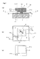
- Figure 1(a) is a cross-sectional configuration diagram illustrating a mounting structure according to Embodiment 1 of the present invention.
- a mounting structure 10 of the present embodiment includes a substrate 1 and an electronic component 3 that is mounted on the surface of the substrate 1. Electrodes 2a and 2b are formed on the surface of the substrate 1. An alumina substrate with favorable heat-radiating properties is used as the substrate 1.
- the electronic component 3 is an LED that has two electrodes 21 a and 21 b. The two electrodes 21a and 21b correspond to a p-electrode and an n-electrode.
- the electrode 2a and the electrode 21a of the electronic component, and the electrode 2b and the electrode 21b of the electronic component are joined at joints 15a and 15b, respectively.
- the joints 15a and 15b are created by subjecting a metal nanoparticle paste material to a heat treatment.
- a convex portion 4 that corresponds to an example of a member of the present invention is provided in the joint 15a.
- the convex portion 4 comes in contact with the electrode 2a of the substrate 1 and the electrode 21a of the electronic component 3, and functions as a spacer that maintains a fixed clearance between the electrode 2a of the substrate 1 and the electrode 21 a of the electronic component 3 at the time of manufacture.
- a material that increases in temperature faster than the metal nanoparticle paste material for producing the joint 15a is used as the material that forms the convex portion 4.
- Figure 1(b) is a plan view that illustrates the substrate 1, the joints 15a and 15b, and the convex portion 4 of the mounting structure 10.
- Figure 1 (c) is a plan view that illustrates the electronic component 3 of the mounting structure 10.
- Figure 1 (b) corresponds to a cross-sectional view of the mounting structure 10 at a position along a line AA' shown in Figure 1(a) .
- the cross-sectional position of Figure 1(a) is shown by a line BCDEF in Figure 1(b) .
- the joint 15a is formed at a portion at which the electrode 2a and the electrode 21a face each other
- the joint 15b is formed at a portion at which the electrode 2b and the electrode 21b face each other.
- three convex portions 4 are provided at a central portion 70 of the joint 15a.
- the term "central portion” refers to a portion that includes not only the center, but also an area in the vicinity of the center.
- reference numeral 71 denotes a peripheral portion of the joint 15a.
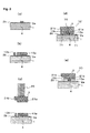
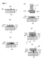
- Figures 2(a)to (e) are views for describing the method of manufacturing the mounting structure 10 of the present embodiment.
- convex portions 4 are formed on the electrode 2a that is formed on the surface of the substrate 1.
- the electrodes 2a and 2b, and the electrodes 21a and 21 b of the electronic component 3 are formed, for example, from gold.
- the electronic component 3 is, for example, an LED device with a sectional shape that is a 10-mm square area.
- the convex portions 4 are composed of gold bumps that are made with a wire bonding apparatus.
- One size of the convex portion 4 is, for example, a diameter of approximately 50 to 80 ⁇ m at a lower part and a diameter of approximately 20 to 30 ⁇ m at an upper part in Figure 2 , and the height thereof can be 30 ⁇ m.
- a step for forming the convex portion 4 corresponds to one example of a member forming step of the present invention.
- a metal nanoparticle paste material is coated on the electrodes 2a and 2b of the substrate 1 to form the bonding material portions 13a and 13b.
- the material used as the metal nanoparticle paste material can be one in which, for example, gold microparticles as metal nanoparticles that are conductive components are dispersed in a solvent.
- the metal nanoparticles are covered by the dispersing agent in the solvent.
- tetradecane can be used as the solvent.
- the dispersing agent for example, one or more kinds of chemical compounds that have a group capable of coordinated binding with a metallic element such as alkylamine can be used.
- the metal nanoparticle paste material can include, for example, 50 weight percent of gold microparticles with a mean particle diameter of 3 to 7 nm, and the density of the gold microparticles can be set to 1.6 g/cc.
- the viscosity of the metal nanoparticle paste material is set to 20 to 50 mPa ⁇ s.
- the metal nanoparticle paste material corresponds to one example of a material used for producing a joint of the present invention, and corresponds to an example of the bonding material of the present invention.
- an ink jet method or a spin coating method or dye coating method or the like can be used as the coating method.
- the bonding material portions 13a and 13b are formed so as to have a comparatively thick thickness.
- the metal nanoparticle paste material has a low viscosity, and therefore coating by an ink jet method can be easily utilized.
- the step of coating a metal nanoparticle paste material corresponds to an example of a coating step of the present invention.
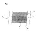
- the term "abut” refers to a state of resisting a pressing force of the electronic component 3 and includes not only a case in which the convex portions 4 are directly contacting the electrode 21a, but also a case as shown in the partially enlarged view in Figure 3 in which a small amount of metal nanoparticle paste material remains between the convex portions 4 and the electrode 21a.
- Figure 3 is a partially enlarged view of Figure 2(d) , in which a portion at which a small amount of metal nanoparticle paste material remains is denoted by reference character S.
- the conditions for curing include inserting a mounting structure 10' in the state shown in Figure 2(d) into a hot air circulating oven and, for example, increasing the temperature to 100°C at a rate of temperature increase of 5°C/min, and thereafter maintaining the temperature at 100°C for 10 minutes.
- This step corresponds to one example of a heat treatment step of the present invention.
- the convex portions 4 when placing the electronic component 3 on the bonding material portions 13a and 13b, the convex portions 4 function as spacers and thus a constant clearance can be maintained between the electrode 2a and the electrode 21 a of the electronic component. Consequently, when performing the heat treatment, it is possible for gas that is generated by heating a dispersing agent component in the bonding material portion 13a to escape to outside from the peripheral portion 71 (see Figure 2(d) ) of the bonding material portion 13a.
- the electrode 2a and the electrode 21 a of the electronic component will come closer than necessary to each other due to the flexibility of the metal nanoparticle paste material, and hence the thickness of the mounting structure will become thin and it will be difficult for gas to escape to outside from the peripheral portion 13e of the bonding material portion 13a. Therefore, air cavities may form in the joint 15a after heat treatment and the bonding strength between the substrate 1 and the electronic component 3 will weaken. Further, the joint may become unstable due to the effect of residual gas when operating the electronic component 3.
- the electrode 2a of the substrate 1 and the electrode 21 a of the electronic component 3 do not come closer to each other than necessary. It is thus possible to suppress the occurrence of a short circuit caused by the metal nanoparticle paste material that forms the bonding material portion 13a between the electrode 2a and the electrode 21 a being pushed out from between the electrodes and contacting the neighboring electrodes 2b and 21b and the metal nanoparticle paste material between the electrodes 2b and 21b. In this connection, pushing out of the metal nanoparticle paste material of the bonding material portion 13b on the electrode 2b and 21b side is also suppressed.
- the convex portions 4 are formed by metal bumps whose temperature rises faster than the temperature of the metal nanoparticle paste material, the convex portions 4 increase in temperature faster than the bonding material portions 13a and 13b during the heat treatment. Consequently, when performing the heat treatment, curing of the metal nanoparticle paste material begins from the metal nanoparticle paste material that is positioned at the central portion 70 and that surrounds the convex portions 4, and gaseous matter such as gas is generated accompanying the start of sintering, and heat is gradually conveyed to the peripheral portion 71 from the central portion 70 and sintering and gas generation occur. Hence, the generated gas can escape efficiently to the outside from the peripheral portion 71 of the bonding material portion 13a.
- each convex portion 4 is used as a spacer to secure a clearance of a fixed amount between the electrode 2a and electrode 21 a. Furthermore, the convex portions 4 are provided as the starting point of gas generation by heat transfer. As a result, it is possible to control the period and location of gas generation, and gas can be allowed to escape to the peripheral portion 71 efficiently from the central portion 70 of the bonding material portion during the heat treatment, so that the joint can be made more reliable.
- a configuration may also be adopted in which the convex portion 4 is used only as a spacer and is not used as a starting point of gas generation by heat transfer.
- a material material with a high thermal conductivity
- the metal nanoparticle paste material need not be used as the material that forms the convex portion 4.
- FIG. 4 is a cross-sectional configuration diagram of a mounting structure 20.
- components that are substantially the same as components of the mounting structure 10 are denoted by the same reference numbers. The same applies with respect to the drawings described hereunder.
- three convex portions 24 that touch the electrode 2a are formed at the central portion 70 of the joint 15a.
- the convex portions 24 are not in contact with the electrode 21 a of the electronic component 3, and do not function as spacers that maintain a clearance between the electrode 2a and the electrode 21 a.
- the convex portions 24 of the mounting structure 20 having this structure increase in temperature faster than the metal nanoparticle paste material, similarly to the present embodiment, and are formed using a material such as gold bumps.
- a gas is generated. The gas can escape from the peripheral portion 71 when the bonding material portion (state before hardening of the joint 15a) is being cured.
- the convex portions 24 do not contact the electrode 21 a of the electronic component 3, physical damage to the electronic component 3 at the time of manufacture can be decreased.
- the height of the convex portions 24 is too low, the proportion of the central portion 70 occupied by the convex portions 24 decreases and the proportion of the central portion 70 occupied by the metal nanoparticle paste material increases, and as a result the amount of gas generated in the central portion 70 will increase. Consequently, it is more preferable to make the height of the convex portions 24 as high as possible.
- the convex portions 4 are provided at the central portion 70 of the joint 15a according to Embodiment 1, in a case where the convex portions 4 are only used as spacers and are not used as the starting point of gas generation by heat transfer, the convex portions 4 may be provided at the peripheral portion 71 and not at the central portion 70 of the joint 15a.
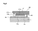
- the convex portion may be provided outside the joint 15a and not inside the joint 15a, as shown in the cross-sectional configuration diagram of a mounting structure 35 shown in Figure 5 .
- a convex portion 46 is provided outside the joint 15a.
- the convex portion 46 is provided on the electrode 2a, and the upper end of the convex portion 46 contacts an electronic component 3'.
- the convex portion 46 functions as a spacer, and since a fixed clearance can be maintained between the electrode 21a and the electrode 2a, a gas that is generated when performing a heat treatment can be allowed to escape efficiently to outside.
- the convex portion 46 may also be provided directly on the substrate 1 rather than on the electrode 2a.
- a configuration in which the convex portion 4 is provided at the central portion 70 of the joint 15a is more preferable since is it possible to suppress the generation of gas itself, because the amount of metal nanoparticle paste material at the central portion 70 is decreased.
- the rate of temperature increase is set to, for example, 5°C/min
- the rate of temperature increase may be appropriately changed depending on the components included in the metal nanoparticle paste material.
- the rate of temperature increase is too fast, bumping of the solvent in the bonding material portion will occur, and bubbles will be unable to escape smoothly from between the electrode 21a of the electronic component and the electrode 2a of the substrate.
- metal bumps are used as the convex portions 4 and the metal bumps have a high thermal conductivity, heat of the electronic component 3 is easily transferred to the substrate 1.
- the metal bumps can be prepared by plating or wire bonding or the like. Further, since the metal bumps have pointed tips, an increasing amount of space can be created towards the upper part of the bumps, and it is easy for the generated gas to escape to outside.
- the convex portions 4 can also be formed on the electronic component 3 side rather than the substrate 1 side, in such case the convex portions 4 may cause physical damage to the electronic component 3. It is therefore preferable to provide the convex portions 4 on the substrate 1 side.
- the electronic component 3 is a semiconductor, because the structure is one that is weak with respect to physical impact due to microfabrication of internal wiring rules, it is advantageous to provide the convex portions 4 on the substrate 1 side.
- the metal nanoparticle paste material is coated on the side of the substrate 1 on which the convex portions 4 are formed, the metal nanoparticle paste material may be coated on the electronic component 3.
- the structure is one that has a portion in which the electrodes 2a and 2b and the electrodes 21a and 21b are facing each other, respectively, a structure may be adopted in which the electrodes 2a and 2b and the electrodes 21a and 21b do not face each other at all.
- the joint 15 is formed only on an electrode, the joint 15 may be formed across a portion on which an electrode is not provided. More specifically, it is sufficient that a connection portion is formed so that an electrode of the substrate and an electrode of the electronic component are electrically connected and the electronic component can be fixed on the surface of the substrate.
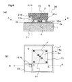
- FIG. 6(a) is a cross-sectional configuration diagram of the mounting structure 30.
- Figure 6(b) is a cross-sectional view along a line AA' in (a). The cross-sectional position of Figure 6(a) is shown by a line BCDEF in Figure 6(b) .
- convex portions 4 comprising a metal bump are also formed at four corners at the peripheral portion 71 of the joint 15.
- a plurality of convex portions 4 are provided more densely at the central portion 70 of the joint 15 that at the peripheral portion 71.
- a clearance between the electrodes can be secured with greater stability, and it is possible for gas to escape to outside from the central portion 70 from which it is hardest for the gas to escape.
- the temperature of the bonding material portion 13a increases faster at the central portion 70 than at the peripheral portion 71 due to the difference in the density of the convex portions 4
- gas generated at the central portion 70 can be allowed to escape to outside efficiently, and the occurrence of air cavities in the joint 15 can be suppressed.
- the bumps are the same as those described in the above described embodiment.
- the number of convex portions 4 is not limited to the structure of the present embodiment, and only one convex portion 4 may be provided at the central portion 70 of the joint 15. However, arranging a further number of convex portions 4 at the periphery of the joint 15 is more preferable because the clearance between the electrode 2a and the electronic component electrode 21a can be maintained fixed overall, and gas can escape easily.
- the size of the convex portion 4 of the present embodiment is also not limited, and one large convex portion may be provided at the central portion 70 of the bonding material portion 13a.
- Figure 7(a) is a cross-sectional configuration diagram of a mounting structure 31
- Figure 7(b) is a cross-sectional view along a line AA' in Figure 7(a) .
- the cross-sectional position of Figure 7(a) is shown by a line BCDEF in Figure 7(b) .
- a single large convex portion 40 is formed at the central portion 70 of the joint 15a.
- the parallelism between the electrode 2a and the electrode 21 a of the electronic component is regulated and a fixed clearance is also secured therebetween, and gas generated during curing of the bonding material portion can be allowed to escape.
- the convex portion 40 can be made by plating. Further, it is necessary to make the upper surface of the convex portion 40 flat.
- the convex portion 40 in the mounting structure 31 shown in Figure 7 is used as a spacer that maintains a clearance between the electrode 2a and the electrode 21a and as a starting point of gas generation by heat transfer, when using the convex portion 40 only as a starting point of gas generation by heat transfer, the convex portion 40 need not contact with the electrode 21a.
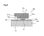
- FIG. 8 A cross-sectional view of the mounting structure 32 in this state is shown in Figure 8 .
- a convex portion 41 that does not contact with the electrode 21a is also shown.
- the cross-sectional position of Figure 8(a) is the same position as in Figure 7(a) .
- the convex portions are manufactured by plating.
- a convex portion is formed by a metal bump
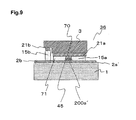
- a convex portion may be formed by fabricating a portion 200a' corresponding to the central portion 70 of the joint 15 of the surface of the electrode 2a in a concavo-convex shape.
- Figure 9 is a cross-sectional configuration diagram of a mounting structure 36.
- an electrode 2a' is provided in which unevenness is formed at the central portion 70.
- a convex portion 45 is composed by the unevenness.
- the convex portion 45 is formed by first performing fabrication to decrease the thickness of portions other than the portion 200a' of the electrode 2a'.
- the electrode 2a' is formed from, for example, gold, the thermal conductivity thereof is better than that of the metal nanoparticle paste material. Consequently, the convex portion 45 composed of unevenness of the electrode 2a' can be used as a starting point of gas generation by heat transfer, and curing of metal nanoparticle paste material at the periphery of the convex portion 45 provided at the central portion 70 can be promoted. When using the convex portion 45 only as a spacer, the convex portion 45 need not be formed at the central portion 70.
- the convex portion 45 is formed by processing the surface of the electrode 2a' of the substrate 1 as shown in Figure 9
- the convex portion may be formed by processing the surface of a substrate 21a of the electronic component 3.
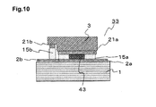
- FIG 10 is a cross-sectional configuration diagram of a mounting structure 33 according to Embodiment 2 of the present invention.
- the mounting structure 33 of Embodiment 2 differs from that of Embodiment 1 in the respect that a single convex portion 43 formed of a conductive paste material is provided at the center of the joint 15.
- components that are substantially the same as components in Embodiment 1 are denoted by the same reference numbers.
- Figure 10 is a cross-sectional view at the same position as in Figure 1(a) .
- the convex portion 43 corresponds to an example of a member of the present invention.
- Figures 11 (a) to (f) are cross-sectional configuration diagrams for describing a method of manufacturing the mounting structure 33.
- a conductive paste material portion 44 at which a conductive paste material is coated on the upper surface of the electrode 2a of the substrate 1 is formed.
- the conductive paste material corresponds to one example of a paste material including a conductive substance of the present invention.
- the conductive paste material is, for example, a silver paste material that includes silver, resin, and a curing agent, and a material is used that has a curing temperature that is equal to or less than the curing temperature of the metal nanoparticle paste material. It is not necessary for the conductive paste material to include metal particles with a mean particle diameter of 50 ⁇ m or less, as in the metal nanoparticle paste material.
- the metal nanoparticle paste material is coated on the electrodes 2a and 2b so as to cover the conductive paste material portion 44 and form the bonding material portions 13a and 13b.
- the step of coating the metal nanoparticle paste material to form the bonding material portions 13a and 13b corresponds to an example of a coating step of the present invention.
- curing of the convex portion 43' that is in a partially cured state and the bonding material portions 13a and 13b is performed by a heat treatment in a hot air circulating oven to form the joints 15a and 15b, and thereby produce the mounting structure 33 shown in Figure 11(f) .
- This step corresponds to one example of a heat treatment step of the present invention.
- the convex portion 43' in a partially cured state is cured prior to the bonding material portions 13a and 13b to form the convex portion 43.
- the conductive paste material portion 44 is cured to form the convex portion 43 prior to curing of the bonding material portions 13a and 13b, and the convex portion 43 is used as a spacer that maintains a clearance between the electrode 2a and the electrode 21 a of the electronic component 3. It is thereby possible to allow gas that is generated from the bonding material portion 13a to escape efficiently to the outside during the heat treatment step.
- the convex portion 43 is provided at the central portion 70 of the bonding material portion 13a, the amount of metal nanoparticle paste material present at the central portion 70 is decreased and generation of gas can itself be suppressed.
- the material used to produce the convex portion 43 is a conductive paste material that, in a partially cured state, increases in temperature faster than the metal nanoparticle paste material that is the material of the bonding material portions 13a and 13b.
- the convex portion serves as a starting point of gas generation by heat transfer, and because curing starts from the central portion 70 of the bonding material portion 13a, the gas can be allowed to escape efficiently to the outside.
- temperatures that are appropriately adjusted can be used for the partial curing temperature and the curing temperature of the conductive paste material that is the material used to produce the convex portion as well as the curing temperature of the metal nanoparticle paste material. Further, it is more preferable to set a difference between the curing temperature of the conductive paste material and the metal nanoparticle paste material to 5°C or more, on the basis of at least a rate of temperature increase of 5°C/minute.
- the convex portion 43' is flexible since it is in a partially cured state when the electrode 21a is pressed thereon. Consequently, as shown in Figure 11(e) , damage to the electrode 21a can be reduced as much as possible when pressing the electronic component 3 against the convex portions 43'.
- curing of the conductive paste material portion 44 may be performed before curing the bonding material portions 13a and 13b, or may be performed at the same time as curing the bonding material portions 13a and 13b.
- the metal nanoparticle paste material need not be coated so as to cover the conductive paste material portion 44 as shown in Figure 11(b) .
- the bonding material portion 13a may be formed in a manner that avoids the conductive paste material portion 44.
- the conductive paste material portion 44 is placed in a partially cured state after the metal nanoparticle paste material is coated so as to cover the conductive paste material portion 44, the conductive paste material portion 44 may be placed in a partially cured state before the metal nanoparticle paste material is coated.
- the conductive paste material portion 44 is in a partially cured state when placing the electronic component 3 thereon, the conductive paste material portion 44 may be in a completely cured state, and the conductive paste material need not be in a partially cured state.
- a conductive paste may be used with respect to which there is little difference between the curing temperature thereof and the curing temperature of the metal nanoparticle paste material, in such case it is not possible to cure only the conductive paste material after coating the metal nanoparticle paste material. Consequently, after coating the conductive paste material on the electrode 2a, it is necessary to cure the conductive paste material before applying the metal nanoparticle paste material. At this time, the conductive paste material may be placed in a partially cured state or in a completely cured state. However, from the point of view that damage to the electrode 21a can be reduced as much as possible, it is more preferable that the conductive paste material portion 44 is in a partially cured state when placing the electronic component thereon.
- the present invention can also be applied to an electronic component with a larger electrode area.
- the bonding material that is a metal nanoparticle paste material is applied using an ink jet method, a method such as printing or the like may be used.
- the conductive paste may be a paste other than a silver paste.
- the convex portion 43 of Embodiment 2 is not limited to the shape shown in Figures 10 and 11 , and may be any of the various shapes described in Embodiment 1.
- Figure 13 is a cross-sectional configuration diagram of a mounting structure 34 according to Embodiment 3 of the present invention.
- the mounting structure 34 according to Embodiment 3 of the present invention has the same basic structure as in Embodiment 1, the material of the convex portion is different.
- the description of Embodiment 3 centers on this point of difference.
- components that are substantially the same as components in Embodiment 1 are denoted by the same reference numbers.
- a convex portion 52 according to Embodiment 3 is produced using a material including an oxide, and is used as an oxygen-supplying material.
- the convex portion 52 corresponds to one example of a "member that has supplied oxygen" of the present invention. Copper oxide, aluminum oxide or the like can be used as the oxide.
- the convex portion can be formed using a paste material in which copper oxide or aluminum oxide powder that has a particle diameter of approximately 1 ⁇ m is mixed with an epoxy resin.
- the composition of the paste material can be such that, for example, the ratio of percentage by weight of oxide to resin is 80:20.
- Figures 14(a) to (f) are views for describing the method of manufacturing the mounting structure 34 of Embodiment 3.
- the above described paste material is coated on the upper portion of the electrode 2a to form an oxygen-supplying material portion 50.
- the material used as the paste material that is a mixture of an oxide and a resin as described above is a material (material with a high thermal conductivity) with a curing temperature that is equal to or less than the curing temperature of the metal nanoparticle paste material and which increases in temperature faster than the metal nanoparticle paste material after curing.
- the metal nanoparticle paste material is coated on the electrodes 2a and 2b so as to cover the oxygen-supplying material portion 50 and thereby form the bonding material portions 13a and 13b. This step of coating the metal nanoparticle paste material corresponds to an example of the coating step of the present invention.
- an oxide is used as a material for producing the convex portion 52
- the oxygen of the oxide contributes to decomposition of the dispersing agent that is present in the bonding material portion 13a, and gasification of the metal nanoparticle paste material around the periphery of the convex portion 52 that is formed using a material including an oxide can be promoted.
- the metal nanoparticle paste material is stabilized by a dispersing agent so that the metal nanoparticles do not polymerize, and polymerization is inhibited by the dispersing agent covering the metal nanoparticles.
- an oxide used in a material for producing the convex portion 52 decomposes the dispersing agent and enables the efficient generation and escape of gas.
- the convex portion 52 formed by a material including an oxide at the central portion 70 of the bonding material by disposing the convex portion 52 formed by a material including an oxide at the central portion 70 of the bonding material, sintering of the metal nanoparticle paste material of the central portion 70 can be promoted, and although curing starts from the central portion 70 of the bonding material portion 13a and gas is generated, because the peripheral portion 71 is not yet cured it is possible for the generated gas to escape to outside from inside the bonding material portion 13a.
- the convex portion is used as a spacer, a starting point of gas generation by heat transfer, as well as a starting point of gas generation by oxygen supply, gas generated inside the bonding material portion can be allowed to escape to outside more efficiently.
- the convex portion 52 contacts with the electrode 2a and the electrode 21 a
- the convex portion 52 may be disposed at the center of the bonding material portion in a condition in which the convex portion 52 does not contact with the electrodes 2a and 21a.
- the paste material when using the convex portion 52 only as an oxygen-supplying material, it is not necessary for the paste material to be a material (material with a high thermal conductivity) that increases in temperature faster than the metal nanoparticle paste material.
- the paste material of the present embodiment may be cured at the same time as the bonding material portions 13a and 13b.
- the paste material can be cured to form the convex portion 52 prior to applying the metal nanoparticle paste material.
- the convex portion 52 can be used as a spacer.
- a material to be used for producing the oxygen-supplying material portion 50 is a material (material with a high thermal conductivity) for which at least a partial curing temperature is equal to or less than a curing temperature of the metal nanoparticle paste material, and which increases in temperature faster than the metal nanoparticle paste material after being partially cured.
- the convex portion 52 of Embodiment 3 is not limited to this shape, and may be any of the various shapes described in Embodiment 1.
- Embodiment 3 oxygen is supplied to the metal nanoparticle paste material at the central portion 70 at the time of a heat treatment by providing the oxygen-supplying member 51, a configuration may also be adopted so as to supply oxygen to the metal nanoparticle paste material at the central portion 70 by placing a portion of either of the electrode 2a and the electrode 21 a that corresponds to the central portion 70 of the joint 15a in an oxidized state.
- a portion of the electrode 2a that corresponds to the central portion 70 corresponds to the portion 200a' shown in Figure 9 .
- a portion of the electrode 21a that corresponds to the central portion 70 corresponds to a portion facing the portion 200a' shown in Figure 9 .
- the convex portion 43 formed by a conductive paste material is provided according to Embodiment 2, by using a metal oxide as a conductive material in the conductive paste material it is possible to also use the convex portion 43 as a starting point of gas generation by oxygen supply.
- the convex portion 52 is produced using a paste material in which a copper oxide or aluminum oxide powder is mixed in a resin
- a structure may also be adopted in which a metal oxide such as copper oxide or aluminum oxide powder is simply placed on the electrode 21a.
- the bonding material portion 13a is formed by placing the metal oxide on the electrode 21a, and thereafter applying the metal nanoparticle paste material from the top thereof.
- the mounting structure is inserted into a hot air circulating oven and the bonding material portions 13a and 13b are cured
- curing of the bonding material portions 13a and 13b may also be performed by placing the mounting structure on a hot plate. At that time, heating from the side of the substrate 1 on which the convex portion is provided is more preferable because the temperature of the convex portion increases faster than the temperature of the bonding material portion 13a as the result of heat transfer from the substrate 1, and the convex portion functions as a starting point of gas generation by heat transfer.
- a convex portion is provided only at the joint 15a on the side of the electrode 2a that has a large area, a convex portion may also be formed at the joint 15b on the electrode 2b side.
- ultrasonic vibrations and not only heating, may be applied in order to cure the bonding material portions 13a and 13b.
- Embodiment 4 Although an LED is used as one example of the electronic component 3 in the foregoing Embodiments 1 to 3, according to Embodiment 4 an IGBT (insulated gate bipolar transistor) is used as the electronic component.
- IGBT insulated gate bipolar transistor
- Embodiment 4 the basic structure and manufacturing method of a joint and a convex portion are the same as in Embodiment 1.
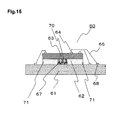
- Figure 15 is a cross-sectional configuration diagram of a mounting structure 60 according to Embodiment 4 of the present invention.
- the mounting structure 60 of Embodiment 4 includes a substrate 61 and an electronic component (IGBT) 63 that is arranged on the top side of the substrate 61 via a joint 62.
- the IGBT is used in a control system of a drive current to a driving device such as a motor, and is a semiconductor device for driving that requires a measure for heat radiation.
- An Si semiconductor may be mentioned as an example of a semiconductor used in an IGBT, and other examples include an SiC semiconductor and a GaN semiconductor.
- An electrode 64 is formed on the upper surface of the electronic component 63.
- the electrode 64 is electrically connected to the substrate 61 by a metal wire 65.
- the electronic component 63 is fixed on the substrate 61 by the joint 62 that is formed by the same metal nanoparticle paste material as in Embodiments 1 to 3. Heat radiation of the electronic component 63 is performed via the joint 62.
- a convex portion 67 that is the same as in Embodiment 1 is formed at a central portion 70 of the joint 62.
- Three convex portions 67 are provided at the central portion 70 of the joint 62. The upper edge of each convex portion 67 abuts against the electronic component 63.
- the joint 62 is not provided between electrodes.
- an example of a joint that has a heat radiation function of the present invention corresponds to the joint 62 of Embodiment 4
- an example of a member of the present invention corresponds to the convex portion 67 of Embodiment 4.
- the mounting structure 60 of Embodiment 4 is manufactured as described below.
- the convex portions 67 are formed by metal bumps on the substrate 1, and a metal nanoparticle paste material is coated on the substrate 1 so as to cover the convex portions 67.
- the electronic component 63 is placed on the metal nanoparticle paste material, and the electronic component 63 is pressed towards the substrate 1 until the electronic component 63 abuts against the convex portions 67.
- the metal nanoparticle paste material is cured by performing a heat treatment to form the joint 62 and fix the electronic component 63 to the substrate 1.
- the electrode 64 of the electronic component 63 and an electrode 68 of the substrate 61 are electrically connected by the metal wire 65 to thereby produce the mounting structure 60 of Embodiment 4.
- Embodiment 4 also, the convex portions 67 are used as spacers at the time of manufacture, and because gas generated at the central portion 70 can be allowed to escape to outside when performing a heat treatment, it is possible to prevent gas retention inside the joint 62. If a case is assumed in which gas remains inside the joint 62, the efficiency of heat radiation with respect to heat of the electronic component 63 being radiated to the substrate via the joint 62 will be poor. However, the heat radiation efficiency can be improved by suppressing gas retention as described in Embodiment 4.
- the convex portion 67 is formed by a metal bump that increases in temperature faster than the metal nanoparticle paste material, the convex portion 67 increases in temperature faster than the metal nanoparticle paste material at the time of a heat treatment. Consequently, when performing the heat treatment, curing of the metal nanoparticle paste material begins from the metal nanoparticle paste material that is positioned at the central portion 70 and that surrounds the convex portions 4, and gaseous matter such as a gas is generated accompanying the start of sintering, and the heat is gradually conveyed to the peripheral portion 71 from the central portion 70 and sintering and gas generation occur. Hence, it is possible to let the generated gas escape efficiently from the joint.
- the convex portion 67 may also be used as a starting point of gas generation by oxygen supply.
- Embodiments 1 to 3 and the modification examples described in each embodiment can be applied to the mounting structure 60 of Embodiment 4. Below, inventions rerated to the present invention will be described.
- the 1 st invention related to the present invention is a mounting structure, comprising:
- the 2 nd invention related to the present invention is a mounting structure, comprising:
- the 3 rd invention related to the present invention is the mounting structure according to the 1 st or 2 nd invention, wherein the member is provided so as to abut against the substrate and so as not to abut against the electronic component.
- the 4 th invention related to the present invention is a method of manufacturing a mounting structure which comprises:
- the 5 th invention related to the present invention is a method of manufacturing a mounting structure which comprises:
- the mounting structure of the present invention and the method of manufacturing the mounting structure are advantageous in that gaseous matter that is generated when performing a heat treatment can be allowed to escape efficiently to outside, and the mounting structure is useful for bonding a semiconductor device to a substrate and the like.
Landscapes
- Engineering & Computer Science (AREA)
- Mechanical Engineering (AREA)
- Manufacturing & Machinery (AREA)
- Microelectronics & Electronic Packaging (AREA)
- Wire Bonding (AREA)
- Electric Connection Of Electric Components To Printed Circuits (AREA)
- Die Bonding (AREA)
- Conductive Materials (AREA)
Abstract
Description
- The present invention relates to a mounting structure and a method of manufacturing the mounting structure.
- A method in which metal nanoparticles are used as a bonding material is receiving attention as a method of mounting an electronic component such as a semiconductor device on a base material made of ceramic or polyimide or the like. The term "metal nanoparticles" refers to metal particles of a size with a mean particle diameter that is less than 50 nm, such as Au, Ag, or Cu (hereunder, referred to as "metal nanoparticles"). Since the surface activity of such metal nanoparticles is high compared to a bulk material as the result of miniaturization, bonding is possible at a low temperature, and a high fusing point that is equivalent to a bulk material is obtained when bonding occurs and the size increases. Consequently, there are expectations regarding the application of methods that use metal nanoparticles as a bonding material to a wide range of products for which a need exists to decrease thermal stress when mounting electronic components and improve a heat resistant temperature after mounting. Further, compared to a conductive paste material that does not use metal nanoparticles, in a conductive paste material that uses metal nanoparticles, since metal is bonded and not merely touching, the resistivity is low and the bonding strength is also enhanced, and thus superior bonding is achieved. A conventional process of mounting an electronic component using such kind of metal nanoparticles as a bonding material is illustrated in
Figures 16 to 18 . -
Figure 16(a), Figure 17(a) , and Figure 18(a) are plan views that illustrate a substrate during a mounting step.Figure 16(b), Figure 17(b) , and Figure 18(b) are cross-sectional views that represent a section along a line GG' inFigure 16(a), Figure 17(a) , and Figure 18(a), respectively. - First, as shown in
Figures 16(a)and (b) , asubstrate 1001 is prepared in whichconductor wiring 1002 is formed on a base material. Next, as shown inFigures 17(a)and (b) , abonding material portion 1013 is formed at component mounting positions on theconductor wiring 1002 using a paste material that includes metal nanoparticles (hereunder, referred to as "metal nanoparticle paste material"). - Next, as shown in Figures 18(a) and (b),
electrodes 1014 of anelectronic component 1003 are positioned facing thebonding material portion 1013, and theelectronic component 1003 is mounted on thesubstrate 1001. Further, by applying energy such as heat to the bondingmaterial portion 1013, thebonding material portion 1013 is bonded and cured to formjoints 1015, and thereby bond theelectrodes 1014 of theelectronic component 1003 and theconductor wiring 1002 of thesubstrate 1001. As a result, as shown in Figures 18(a) and (b), a mounting structure is produced in which theelectrodes 1014 of theelectronic component 1003, thejoints 1015, and theconductor wiring 1002 are connected in that order in a layered structure. - The metal nanoparticle paste material is stabilized by means of a dispersing agent to prevent polymerization of the metal nanoparticles. By applying energy such as heat to the metal nanoparticle paste material, the dispersing agent in the bonding
material portion 1013 is decomposed using oxygen, so that metal nanoparticles fuse together and bond to form thejoint 1015. - A method has been proposed that uses this kind of metal nanoparticle paste material when mounting an LED as an electronic component (for example, see Patent Document 1). According to
Patent Document 1, a metal nanoparticle paste is cured by applying ultrasonic vibrations thereto. However, when using ultrasonic vibrations, in some cases damage is caused to the electronic components or the bonding is insufficient. Hence, a method has also been proposed in which curing is performed by heating in the same way as described above together with the use of ultrasonic vibrations or instead of using ultrasonic vibrations. - Patent Document 1: Japanese Patent Laid-Open No.
2005-136399 - However, according to the conventional mounting structure described above, although when the substrate and electrode area of an electronic component is small it is possible for gaseous matter such as gas that is generated when heating the
bonding material portion 1013 to escape into the air, when the electrode area is large, there is the problem that gaseous matter such as gas can not escape into the air. This problem is described in detail below. -
Figures 19(a) to (f) are views that illustrate a method of manufacturing amounting structure 100 when mounting an LED as an electronic component. When using an LED device as an electronic component, as shown inFigure 19(a) , the substrate electrodes include anelectrode 2a and anelectrode 2b of different sizes. - As shown in
Figure 19(b) , a metal nanoparticle paste material is coated on theelectrodes material portions - The
electronic component 3 that is an LED haselectrodes electrodes substrate 1. Next, as shown inFigure 19(c) , a face of theelectronic component 3 on a side opposite the side on which theelectrodes mounting tool 16, and theelectronic component 3 is placed on thebonding material portions Figure 19(d) ). Thereafter, drying and a heat treatment is performed, so that the metal nanoparticle paste material of thebonding material portions joints Figure 19(e) ). - Since heat and oxygen are required for decomposition of a dispersing agent when performing heat treatment, it is easier for oxygen to be supplied at the peripheral portion of the bonding material portion rather than from the central portion, because the peripheral portion is touching the external air. As a result, there is a tendency for the curing rate to be faster at the peripheral portion than at the central portion of the bonding material portion. In the case of using a common semiconductor chip as an electronic component, accompanying microfabrication, an electrode thereof is the size of an area of several tens of µm square or less, and the width of the wiring is 100 µm or less. Hence, there is little difference between the curing rate at a peripheral portion and a central portion of the bonding material portion. Consequently, a gas can be allowed to escape from within the metal nanoparticle paste material.
- However, since the
electrodes bonding material portion 13a shown inFigure 19(f) , aperipheral portion 13e of thebonding material portion 13a is cured first, and thereafter the central portion is cured. Consequently, it is difficult to let agas 22 that arises in the vicinity of the central portion escape to outside of the bondingmaterial portion 13a. As a result, the gas is liable to remain inside the joint 15 after the heat treatment, and a bonding failure may occur. - Further, when the
bonding material portion 13a is made with a thin thickness, the area of a portion at which gas generated at the central portion escapes decreases. Consequently, the gas is more liable to remain after the heat treatment. - The present invention has been made in view of the problems associated with the conventional mounting structure, and an object of the invention is to provide a mounting structure that can efficiently allow gaseous matter that is generated when performing a heat treatment to escape to outside, as well as a method of manufacturing the mounting structure.
- In order to solve the above problem, the 1st aspect of the present invention is a mounting structure, comprising:
- a substrate;
- an electronic component;
- a joint which fixes the electronic component to a surface of the substrate, and which is made of a metal nanoparticle paste material; and
- a member which abuts against the electronic component and the substrate, and which is used as a spacer.
- Furthermore, the 2nd aspect of the present invention is the mounting structure according to the 1st aspect of the present invention, wherein the member is embedded at a central portion of the joint, and is made of a material with a higher thermal conductivity than the metal nanoparticle paste material.
- Furthermore, the 3rd aspect of the present invention is the mounting structure according to the 1st aspect of the present invention, wherein the member is a member which is embedded at a central portion of the joint, and which has supplied oxygen to the metal nanoparticle paste material.
- Furthermore, the 4th aspect of the present invention is the mounting structure according to any of the 1st to 3rd aspects of the present invention, wherein:
- the substrate has an electrode;
- the electronic component has an electrode;
- the joint electrically connects the electrode of the substrate and the electrode of the electronic component; and
- the member abuts against the electrode of the electronic component and the electrode of the substrate.
- Furthermore, the 5th aspect of the present invention is the mounting structure according to the 4th aspect of the present invention, wherein the member is formed by unevenness on a surface of the electrode of the substrate or the electrode of the electronic component.
- Furthermore, the 6th aspect of the present invention is the mounting structure according to the 1st aspect of the present invention, wherein the joint has a heat radiation function.
- Furthermore, the 7th aspect of the present invention is the mounting structure according to any of the 1st to 3rd aspects of the present invention, wherein:
- a plurality of the members are provided; and
- the plurality of the members are provided more densely at the central portion than a peripheral portion of the joint.
- Furthermore, the 8th aspect of the present invention is the mounting structure according to the 4th aspect of the present invention, wherein:
- the electrode of the substrate and the electrode of the electronic component are provided so as to at least partly face each other; and
- the joint is provided at least between portions of the electrodes, which are provided so as to face each other.
- Furthermore, the 9th aspect of the present invention is the mounting structure according to the 1st or 2nd aspect of the present invention, wherein the member is formed by a bump.
- Furthermore, the 10th aspect of the present invention is the mounting structure according to any of any of the 1st to 3rd aspects of the present invention, wherein the member is made using a paste material which includes a conductive substance.
- Furthermore, the 11th aspect of the present invention is the mounting structure according to the 3rd aspect of the present invention, wherein the member is made using a paste material in which a metal oxide and a resin are mixed.
- Furthermore, the 12th aspect of the present invention is the mounting structure according to the 3rd aspect of the present invention, wherein the member is made using a metal oxide.
- Furthermore, the 13th aspect of the present invention is the mounting structure according to any of the 1st to 3rd aspects of the present invention, wherein the member is made of a material with a lower curing temperature than the metal nanoparticle paste material of which the joint is made.
- Furthermore, the 14th aspect of the present invention is the mounting structure according to any of the 1st to 3rd aspects of the present invention, wherein the metal nanoparticle paste material includes metal particles of 50 nm or less.
- Furthermore, the 15th aspect of the present invention is the mounting structure according to the 4th aspect of the present invention, wherein a portion of either of the electrode of the substrate and the electrode of the electronic component, which corresponds to the central portion of the joint, is formed of a material which has supplied oxygen to the metal nanoparticle paste material.
- Furthermore, the 16th aspect of the present invention is a method of manufacturing a mounting structure which comprises:
- a substrate;
- an electronic component;
- a joint which fixes the electronic component to a surface of the substrate, and which is made of a metal nanoparticle paste material; and
- a member which is provided, as a spacer which abuts against the electronic component and the substrate, in the joint,
- the method comprising:
- a member forming step that forms a member which is used as the spacer on the substrate or the electronic component;
- a coating step that coats the metal nanoparticle paste material on the substrate or the electronic component;
- an arrangement step that arranges the substrate and the electronic component so as to sandwich the metal nanoparticle paste material which is coated; and
- a heat treatment step that cures the metal nanoparticle paste material by applying, after the arrangement step, heat to the metal nanoparticle paste material, and that forms the joint.
- Furthermore, the 17th aspect of the present invention is the method of manufacturing a mounting structure according to the 16th aspect of the present invention, wherein:
- the member is provided at a central portion of the joint; and
- in the heat treatment step, a material of which the member is made increases in temperature faster than the metal nanoparticle paste material.
- Furthermore, the 18th aspect of the present invention is the method of manufacturing a mounting structure according to the 16th aspect of the present invention, wherein:
- the member is provided at a central portion of the joint; and
- in the heat treatment step, the member supplies oxygen to the metal nanoparticle paste material.
- According to the present invention, a mounting structure can be provided which allows gaseous matter that is generated when performing a heat treatment to escape to outside efficiently, as well as a method of manufacturing the mounting structure.
-
- [
Figure 1] Figure 1(a) is a cross-sectional configuration diagram of a mountingstructure 10 according toEmbodiment 1 of the present invention,Figure 1(b) is a cross-sectional view along a line AA' inFigure 1(a), and Figure 1(c) is a back view of anelectronic component 3. - [
Figure 2]Figures 2(a) to (e) are views for describing a method of manufacturing the mountingstructure 10 ofEmbodiment 1 according to the present invention. - [
Figure 3] Figure 3 is a view that illustrates an example of a state in which convex portions on the mounting structure abut against an electrode according toEmbodiment 1 of the present invention. - [
Figure 4] Figure 4 is a cross-sectional configuration diagram of a mountingstructure 20 that is a modification example ofEmbodiment 1 according to the present invention. - [
Figure 5 ] Figure 5(a) is a cross-sectional configuration diagram of a mountingstructure 30 that is a modification example ofEmbodiment 1 according to the present invention, and Figure 5(b) is a cross-sectional view along a line AA' in Figure (a). - [
Figure 6] Figure 6(a) is a cross-sectional configuration diagram of a mountingstructure 31 that is a modification example ofEmbodiment 1 according to the present invention, andFigure 6(b) is a cross-sectional view along a line AA' inFigure 6(a) . - [
Figure 7] Figure 7 is a cross-sectional configuration diagram of a mountingstructure 32 that is a modification example ofEmbodiment 1 according to the present invention. - [
Figure 8] Figure 8 is a cross-sectional configuration diagram of a mountingstructure 35 that is a modification example ofEmbodiment 1 according to the present invention. - [
Figure 9] Figure 9 is a cross-sectional configuration diagram of a mountingstructure 36 that is a modification example ofEmbodiment 1 according to the present invention. - [
Figure 10] Figure 10 is a cross-sectional configuration diagram of a mountingstructure 33 according to Embodiment 2 of the present invention. - [
Figure 11]Figures 11(a) to (f) are views for describing a method of manufacturing the mountingstructure 33 of Embodiment 2 according to the present invention. - [
Figure 12] Figure 12 is a view for describing a modification example of a method of manufacturing the mountingstructure 33 of Embodiment 2 according to the present invention. - [
Figure 13] Figure 13 is a cross-sectional configuration diagram of a mountingstructure 34 according toEmbodiment 3 of the present invention. - [
Figure 14] Figures 14(a) to (f) are views for describing a method of manufacturing the mountingstructure 34 ofEmbodiment 3 according to the present invention. - [
Figure 15] Figure 15 is a cross-sectional configuration diagram of a mountingstructure 60 according toEmbodiment 4 of the present invention. - [
Figure 16] Figures 16(a) and (b) are views for describing a method of manufacturing a conventional mounting structure. - [
Figure 17] Figures 17(a) and (b) are views for describing a method of manufacturing a conventional mounting structure. - [
Figure 18 ] Figures 18(a) and (b) are views for describing a method of manufacturing a conventional mounting structure. - [
Figure 19]Figures 19(a) to (f) are views for describing a method of manufacturing a conventional mounting structure. - Embodiments of the present invention are described hereunder based on the attached drawings.
-
Figure 1(a) is a cross-sectional configuration diagram illustrating a mounting structure according toEmbodiment 1 of the present invention. - A mounting
structure 10 of the present embodiment includes asubstrate 1 and anelectronic component 3 that is mounted on the surface of thesubstrate 1.Electrodes substrate 1. An alumina substrate with favorable heat-radiating properties is used as thesubstrate 1. Theelectronic component 3 is an LED that has twoelectrodes electrodes - The
electrode 2a and theelectrode 21a of the electronic component, and theelectrode 2b and theelectrode 21b of the electronic component are joined atjoints joints - A
convex portion 4 that corresponds to an example of a member of the present invention is provided in the joint 15a. Theconvex portion 4 comes in contact with theelectrode 2a of thesubstrate 1 and theelectrode 21a of theelectronic component 3, and functions as a spacer that maintains a fixed clearance between theelectrode 2a of thesubstrate 1 and theelectrode 21 a of theelectronic component 3 at the time of manufacture. - A material that increases in temperature faster than the metal nanoparticle paste material for producing the joint 15a, more specifically, a material with a high thermal conductivity, is used as the material that forms the
convex portion 4. -
Figure 1(b) is a plan view that illustrates thesubstrate 1, thejoints convex portion 4 of the mountingstructure 10.Figure 1 (c) is a plan view that illustrates theelectronic component 3 of the mountingstructure 10. In this connection,Figure 1 (b) corresponds to a cross-sectional view of the mountingstructure 10 at a position along a line AA' shown inFigure 1(a) . The cross-sectional position ofFigure 1(a) is shown by a line BCDEF inFigure 1(b) . - As shown in
Figures 1(a)to (c) , the joint 15a is formed at a portion at which theelectrode 2a and theelectrode 21a face each other, and the joint 15b is formed at a portion at which theelectrode 2b and theelectrode 21b face each other. As shown inFigure 1(b) , threeconvex portions 4 are provided at acentral portion 70 of the joint 15a. In the present application, the term "central portion" refers to a portion that includes not only the center, but also an area in the vicinity of the center. Further, in the drawings,reference numeral 71 denotes a peripheral portion of the joint 15a. - Next, a method of manufacturing the mounting
structure 10 of the present embodiment is described.Figures 2(a)to (e) are views for describing the method of manufacturing the mountingstructure 10 of the present embodiment. - First, as shown in
Figure 2(a) ,convex portions 4 are formed on theelectrode 2a that is formed on the surface of thesubstrate 1. Theelectrodes electrodes electronic component 3 are formed, for example, from gold. Theelectronic component 3 is, for example, an LED device with a sectional shape that is a 10-mm square area. Theconvex portions 4 are composed of gold bumps that are made with a wire bonding apparatus. One size of theconvex portion 4 is, for example, a diameter of approximately 50 to 80 µm at a lower part and a diameter of approximately 20 to 30 µm at an upper part inFigure 2 , and the height thereof can be 30 µm. A step for forming theconvex portion 4 corresponds to one example of a member forming step of the present invention. - Next, as shown in
Figure 2(b) , a metal nanoparticle paste material is coated on theelectrodes substrate 1 to form thebonding material portions - For example, an ink jet method or a spin coating method or dye coating method or the like can be used as the coating method. After performing a coating step two or three times so as to envelop the
convex portions 4 using the coating method, thebonding material portions - Thereafter, as shown in
Figure 2(c) , theelectronic component 3 is held with the mountingtool 16 and placed over thebonding material portions Figure 2(d) , theelectronic component 3 is pressed against thebonding material portions electrode 21 a abuts against the upper end of theconvex portions 4. This step corresponds to one example of an arrangement step of the present invention. In the present specification, the term "abut" refers to a state of resisting a pressing force of theelectronic component 3 and includes not only a case in which theconvex portions 4 are directly contacting theelectrode 21a, but also a case as shown in the partially enlarged view inFigure 3 in which a small amount of metal nanoparticle paste material remains between theconvex portions 4 and theelectrode 21a. In this connection,Figure 3 is a partially enlarged view ofFigure 2(d) , in which a portion at which a small amount of metal nanoparticle paste material remains is denoted by reference character S. - Finally, curing of the
bonding material portions joints structure 10 shown inFigure 2(e) . The conditions for curing include inserting a mounting structure 10' in the state shown inFigure 2(d) into a hot air circulating oven and, for example, increasing the temperature to 100°C at a rate of temperature increase of 5°C/min, and thereafter maintaining the temperature at 100°C for 10 minutes. This step corresponds to one example of a heat treatment step of the present invention. - According to the present embodiment, when placing the
electronic component 3 on thebonding material portions convex portions 4 function as spacers and thus a constant clearance can be maintained between theelectrode 2a and theelectrode 21 a of the electronic component. Consequently, when performing the heat treatment, it is possible for gas that is generated by heating a dispersing agent component in thebonding material portion 13a to escape to outside from the peripheral portion 71 (seeFigure 2(d) ) of thebonding material portion 13a. - For example, if a case is assumed in which the
convex portions 4 are not present, when placing theelectronic component 3 on thebonding material portions electrode 2a and theelectrode 21 a of the electronic component will come closer than necessary to each other due to the flexibility of the metal nanoparticle paste material, and hence the thickness of the mounting structure will become thin and it will be difficult for gas to escape to outside from theperipheral portion 13e of thebonding material portion 13a. Therefore, air cavities may form in the joint 15a after heat treatment and the bonding strength between thesubstrate 1 and theelectronic component 3 will weaken. Further, the joint may become unstable due to the effect of residual gas when operating theelectronic component 3. - In contrast, by providing the
convex portions 4 that function as spacers as in the present embodiment, theelectrode 2a of thesubstrate 1 and theelectrode 21 a of theelectronic component 3 do not come closer to each other than necessary. It is thus possible to suppress the occurrence of a short circuit caused by the metal nanoparticle paste material that forms thebonding material portion 13a between theelectrode 2a and theelectrode 21 a being pushed out from between the electrodes and contacting the neighboringelectrodes electrodes bonding material portion 13b on theelectrode - Since
convex portions 4 are provided at thecentral portion 70 of thebonding material portion 13a, there is less metal nanoparticle paste material present at thecentral portion 70 and thus the occurrence of gas can itself be suppressed. - Further, according to the present embodiment, since the
convex portions 4 are formed by metal bumps whose temperature rises faster than the temperature of the metal nanoparticle paste material, theconvex portions 4 increase in temperature faster than thebonding material portions central portion 70 and that surrounds theconvex portions 4, and gaseous matter such as gas is generated accompanying the start of sintering, and heat is gradually conveyed to theperipheral portion 71 from thecentral portion 70 and sintering and gas generation occur. Hence, the generated gas can escape efficiently to the outside from theperipheral portion 71 of thebonding material portion 13a. - According to the present embodiment, each
convex portion 4 is used as a spacer to secure a clearance of a fixed amount between theelectrode 2a andelectrode 21 a. Furthermore, theconvex portions 4 are provided as the starting point of gas generation by heat transfer. As a result, it is possible to control the period and location of gas generation, and gas can be allowed to escape to theperipheral portion 71 efficiently from thecentral portion 70 of the bonding material portion during the heat treatment, so that the joint can be made more reliable. - In comparison to the mounting
structure 10 of the present embodiment, in a mounting structure that is made without formingconvex portions 4, bubbles remain in thebonding material portion 13a and connection failures and the like occur. - In this connection, a configuration may also be adopted in which the
convex portion 4 is used only as a spacer and is not used as a starting point of gas generation by heat transfer. In this case, a material (material with a high thermal conductivity) that undergoes a temperature increase faster than the metal nanoparticle paste material need not be used as the material that forms theconvex portion 4. - Further, a configuration may be adopted in which the
convex portion 4 is used only as a starting point of gas generation by heat transfer, and is not used as a spacer. In this case, it is not necessary for theconvex portion 4 to contact both theelectrode 2a and theelectrode 21a, and it is sufficient that theconvex portion 4 contacts at least either one of theelectrode 2a and theelectrode 21a and that heat is transferred. An example of a mounting structure in this case is shown inFigure 4. Figure 4 is a cross-sectional configuration diagram of a mountingstructure 20. In this connection, components that are substantially the same as components of the mountingstructure 10 are denoted by the same reference numbers. The same applies with respect to the drawings described hereunder. - In the mounting
structure 20, threeconvex portions 24 that touch theelectrode 2a are formed at thecentral portion 70 of the joint 15a. Theconvex portions 24 are not in contact with theelectrode 21 a of theelectronic component 3, and do not function as spacers that maintain a clearance between theelectrode 2a and theelectrode 21 a. - The
convex portions 24 of the mountingstructure 20 having this structure increase in temperature faster than the metal nanoparticle paste material, similarly to the present embodiment, and are formed using a material such as gold bumps. Hence, when performing a heat treatment, curing of the metal nanoparticle paste material begins with theconvex portions 24 as a starting point, and in accompaniment therewith a gas is generated. The gas can escape from theperipheral portion 71 when the bonding material portion (state before hardening of the joint 15a) is being cured. - Further, because the
convex portions 24 do not contact theelectrode 21 a of theelectronic component 3, physical damage to theelectronic component 3 at the time of manufacture can be decreased. However, if the height of theconvex portions 24 is too low, the proportion of thecentral portion 70 occupied by theconvex portions 24 decreases and the proportion of thecentral portion 70 occupied by the metal nanoparticle paste material increases, and as a result the amount of gas generated in thecentral portion 70 will increase. Consequently, it is more preferable to make the height of theconvex portions 24 as high as possible. - Although the
convex portions 4 are provided at thecentral portion 70 of the joint 15a according toEmbodiment 1, in a case where theconvex portions 4 are only used as spacers and are not used as the starting point of gas generation by heat transfer, theconvex portions 4 may be provided at theperipheral portion 71 and not at thecentral portion 70 of the joint 15a. - Furthermore, the convex portion may be provided outside the joint 15a and not inside the joint 15a, as shown in the cross-sectional configuration diagram of a mounting
structure 35 shown inFigure 5 . In the mountingstructure 35 shown inFigure 5 , aconvex portion 46 is provided outside the joint 15a. Theconvex portion 46 is provided on theelectrode 2a, and the upper end of theconvex portion 46 contacts an electronic component 3'. With this configuration also, theconvex portion 46 functions as a spacer, and since a fixed clearance can be maintained between theelectrode 21a and theelectrode 2a, a gas that is generated when performing a heat treatment can be allowed to escape efficiently to outside. In this connection, theconvex portion 46 may also be provided directly on thesubstrate 1 rather than on theelectrode 2a. - However, a configuration in which the
convex portion 4 is provided at thecentral portion 70 of the joint 15a is more preferable since is it possible to suppress the generation of gas itself, because the amount of metal nanoparticle paste material at thecentral portion 70 is decreased. - Although according to the above described embodiment the rate of temperature increase is set to, for example, 5°C/min, the rate of temperature increase may be appropriately changed depending on the components included in the metal nanoparticle paste material. However, if the rate of temperature increase is too fast, bumping of the solvent in the bonding material portion will occur, and bubbles will be unable to escape smoothly from between the
electrode 21a of the electronic component and theelectrode 2a of the substrate. - According to the present embodiment, as shown in
Figure 2(b) , since metal bumps are used as theconvex portions 4 and the metal bumps have a high thermal conductivity, heat of theelectronic component 3 is easily transferred to thesubstrate 1. The metal bumps can be prepared by plating or wire bonding or the like. Further, since the metal bumps have pointed tips, an increasing amount of space can be created towards the upper part of the bumps, and it is easy for the generated gas to escape to outside. - In this connection, although the
convex portions 4 can also be formed on theelectronic component 3 side rather than thesubstrate 1 side, in such case theconvex portions 4 may cause physical damage to theelectronic component 3. It is therefore preferable to provide theconvex portions 4 on thesubstrate 1 side. In particular, if theelectronic component 3 is a semiconductor, because the structure is one that is weak with respect to physical impact due to microfabrication of internal wiring rules, it is advantageous to provide theconvex portions 4 on thesubstrate 1 side. - Although according to the present embodiment the metal nanoparticle paste material is coated on the side of the
substrate 1 on which theconvex portions 4 are formed, the metal nanoparticle paste material may be coated on theelectronic component 3. - Further, according to the present embodiment, although the structure is one that has a portion in which the
electrodes electrodes electrodes electrodes - Although according to the present embodiment three
convex portions 4 are formed at thecentral portion 70 of thebonding material portion 13a, the present invention is not limited thereto. For example, a configuration may be adopted as illustrated in a mountingstructure 30 inFigure 6(a) and Figure 6(b). Figure 6(a) is a cross-sectional configuration diagram of the mountingstructure 30.Figure 6(b) is a cross-sectional view along a line AA' in (a). The cross-sectional position ofFigure 6(a) is shown by a line BCDEF inFigure 6(b) . In comparison to the mountingstructure 10 of the present embodiment, in the mountingstructure 30,convex portions 4 comprising a metal bump are also formed at four corners at theperipheral portion 71 of the joint 15. According to the mountingstructure 30, a plurality ofconvex portions 4 are provided more densely at thecentral portion 70 of the joint 15 that at theperipheral portion 71. By arranging theconvex portions 4 in this manner, a clearance between the electrodes can be secured with greater stability, and it is possible for gas to escape to outside from thecentral portion 70 from which it is hardest for the gas to escape. Further, since the temperature of thebonding material portion 13a increases faster at thecentral portion 70 than at theperipheral portion 71 due to the difference in the density of theconvex portions 4, gas generated at thecentral portion 70 can be allowed to escape to outside efficiently, and the occurrence of air cavities in the joint 15 can be suppressed. In this connection, the bumps are the same as those described in the above described embodiment. - The number of
convex portions 4 is not limited to the structure of the present embodiment, and only oneconvex portion 4 may be provided at thecentral portion 70 of the joint 15. However, arranging a further number ofconvex portions 4 at the periphery of the joint 15 is more preferable because the clearance between theelectrode 2a and theelectronic component electrode 21a can be maintained fixed overall, and gas can escape easily. - The size of the
convex portion 4 of the present embodiment is also not limited, and one large convex portion may be provided at thecentral portion 70 of thebonding material portion 13a.Figure 7(a) is a cross-sectional configuration diagram of a mountingstructure 31, andFigure 7(b) is a cross-sectional view along a line AA' inFigure 7(a) . The cross-sectional position ofFigure 7(a) is shown by a line BCDEF inFigure 7(b) . In the mountingstructure 31, a single largeconvex portion 40 is formed at thecentral portion 70 of the joint 15a. By means of this largeconvex portion 40, the parallelism between theelectrode 2a and theelectrode 21 a of the electronic component is regulated and a fixed clearance is also secured therebetween, and gas generated during curing of the bonding material portion can be allowed to escape. Theconvex portion 40 can be made by plating. Further, it is necessary to make the upper surface of theconvex portion 40 flat. Although theconvex portion 40 in the mountingstructure 31 shown inFigure 7 is used as a spacer that maintains a clearance between theelectrode 2a and theelectrode 21a and as a starting point of gas generation by heat transfer, when using theconvex portion 40 only as a starting point of gas generation by heat transfer, theconvex portion 40 need not contact with theelectrode 21a. A cross-sectional view of the mountingstructure 32 in this state is shown inFigure 8 . Aconvex portion 41 that does not contact with theelectrode 21a is also shown. The cross-sectional position of Figure 8(a) is the same position as inFigure 7(a) . - In the case of the mounting
structures structures - Although according to the mounting
structure 10 of Embodiment 1 a convex portion is formed by a metal bump, a convex portion may be formed by fabricating aportion 200a' corresponding to thecentral portion 70 of the joint 15 of the surface of theelectrode 2a in a concavo-convex shape.Figure 9 is a cross-sectional configuration diagram of a mountingstructure 36. In the mountingstructure 36 shown inFigure 9 , instead of theelectrode 2a of thesubstrate 1 described above, anelectrode 2a' is provided in which unevenness is formed at thecentral portion 70. Aconvex portion 45 is composed by the unevenness. Theconvex portion 45 is formed by first performing fabrication to decrease the thickness of portions other than theportion 200a' of theelectrode 2a'. Cutting or grinding or the like is used for the fabrication operation. Next, portions other than theportion 200a' of theelectrode 2a' are masked, and a concavo-convex shape can be formed at theportion 200a' by a sandblast process or the like. - Further, since the
electrode 2a' is formed from, for example, gold, the thermal conductivity thereof is better than that of the metal nanoparticle paste material. Consequently, theconvex portion 45 composed of unevenness of theelectrode 2a' can be used as a starting point of gas generation by heat transfer, and curing of metal nanoparticle paste material at the periphery of theconvex portion 45 provided at thecentral portion 70 can be promoted. When using theconvex portion 45 only as a spacer, theconvex portion 45 need not be formed at thecentral portion 70. - Further, although the
convex portion 45 is formed by processing the surface of theelectrode 2a' of thesubstrate 1 as shown inFigure 9 , the convex portion may be formed by processing the surface of asubstrate 21a of theelectronic component 3. - Next, Embodiment 2 of the present invention is described.
-
Figure 10 is a cross-sectional configuration diagram of a mountingstructure 33 according to Embodiment 2 of the present invention. As shown inFigure 10 , the mountingstructure 33 of Embodiment 2 differs from that ofEmbodiment 1 in the respect that a singleconvex portion 43 formed of a conductive paste material is provided at the center of the joint 15. In this connection, components that are substantially the same as components inEmbodiment 1 are denoted by the same reference numbers.Figure 10 is a cross-sectional view at the same position as inFigure 1(a) . Theconvex portion 43 corresponds to an example of a member of the present invention. - Next, the method of manufacturing the mounting
structure 33 according to Embodiment 2 is described. -
Figures 11 (a) to (f) are cross-sectional configuration diagrams for describing a method of manufacturing the mountingstructure 33. - First, as shown in
Figure 11(a) , a conductivepaste material portion 44 at which a conductive paste material is coated on the upper surface of theelectrode 2a of thesubstrate 1 is formed. The conductive paste material corresponds to one example of a paste material including a conductive substance of the present invention. The conductive paste material is, for example, a silver paste material that includes silver, resin, and a curing agent, and a material is used that has a curing temperature that is equal to or less than the curing temperature of the metal nanoparticle paste material. It is not necessary for the conductive paste material to include metal particles with a mean particle diameter of 50 µm or less, as in the metal nanoparticle paste material. - Next, as shown in
Figure 11(b) , the metal nanoparticle paste material is coated on theelectrodes paste material portion 44 and form thebonding material portions bonding material portions - Thereafter, by heating at a temperature at which the conductive paste material partially cures that is a temperature that is less than the curing temperature of the metal nanoparticle paste material, as shown in
Figure 11 (c) , only the conductivepaste material portion 44 partially cures to form a convex portion 43'. The step of coating and curing the conductive paste material to form the convex portions 43' corresponds to an example of a member forming step of the present invention. - Next, as shown in
Figure 11 (d) , theelectronic component 3 is held with the mountingtool 16 and placed over thebonding material portions electronic component 3 is pressed against thebonding material portions electrode 21 a abuts against the upper end of the convex portion 43 (seeFigure 11 (e) ). This step corresponds to an example of an arrangement step of the present invention. - Finally, curing of the convex portion 43' that is in a partially cured state and the
bonding material portions joints structure 33 shown inFigure 11(f) . This step corresponds to one example of a heat treatment step of the present invention. By means of this heat treatment, the convex portion 43' in a partially cured state is cured prior to thebonding material portions convex portion 43. - Thus, the conductive
paste material portion 44 is cured to form theconvex portion 43 prior to curing of thebonding material portions convex portion 43 is used as a spacer that maintains a clearance between theelectrode 2a and theelectrode 21 a of theelectronic component 3. It is thereby possible to allow gas that is generated from thebonding material portion 13a to escape efficiently to the outside during the heat treatment step. - Further, since the
convex portion 43 is provided at thecentral portion 70 of thebonding material portion 13a, the amount of metal nanoparticle paste material present at thecentral portion 70 is decreased and generation of gas can itself be suppressed. - The material used to produce the
convex portion 43 is a conductive paste material that, in a partially cured state, increases in temperature faster than the metal nanoparticle paste material that is the material of thebonding material portions central portion 70 of thebonding material portion 13a, the gas can be allowed to escape efficiently to the outside. - In this connection, temperatures that are appropriately adjusted can be used for the partial curing temperature and the curing temperature of the conductive paste material that is the material used to produce the convex portion as well as the curing temperature of the metal nanoparticle paste material. Further, it is more preferable to set a difference between the curing temperature of the conductive paste material and the metal nanoparticle paste material to 5°C or more, on the basis of at least a rate of temperature increase of 5°C/minute. This is because a 5°C difference between the curing temperatures means that the conductive paste material cures faster than the metal nanoparticle paste material by a period of approximately one minute, and it is thus possible to prevent adverse effects on the curing of the conductive paste material that are caused by gas that is generated when curing the metal nanoparticle paste material.
- The convex portion 43' is flexible since it is in a partially cured state when the
electrode 21a is pressed thereon. Consequently, as shown inFigure 11(e) , damage to theelectrode 21a can be reduced as much as possible when pressing theelectronic component 3 against the convex portions 43'. - When using the
convex portion 43 as a starting point of gas generation by heat transfer and not using theconvex portion 43 as a spacer for securing a clearance between electrodes, curing of the conductivepaste material portion 44 may be performed before curing thebonding material portions bonding material portions - Further, the metal nanoparticle paste material need not be coated so as to cover the conductive
paste material portion 44 as shown inFigure 11(b) . Instead, as shown inFigure 12 , thebonding material portion 13a may be formed in a manner that avoids the conductivepaste material portion 44. - Although according to the present embodiment the conductive
paste material portion 44 is placed in a partially cured state after the metal nanoparticle paste material is coated so as to cover the conductivepaste material portion 44, the conductivepaste material portion 44 may be placed in a partially cured state before the metal nanoparticle paste material is coated. When there is a possibility of these two materials blending, it is more preferable to partially cure the conductivepaste material portion 44 before the metal nanoparticle paste material is coated, as it is thereby possible to reliably prevent mixing of the conductive paste material and the metal nanoparticle paste material. - Although according to the present embodiment the conductive
paste material portion 44 is in a partially cured state when placing theelectronic component 3 thereon, the conductivepaste material portion 44 may be in a completely cured state, and the conductive paste material need not be in a partially cured state. - Although a conductive paste may be used with respect to which there is little difference between the curing temperature thereof and the curing temperature of the metal nanoparticle paste material, in such case it is not possible to cure only the conductive paste material after coating the metal nanoparticle paste material. Consequently, after coating the conductive paste material on the
electrode 2a, it is necessary to cure the conductive paste material before applying the metal nanoparticle paste material. At this time, the conductive paste material may be placed in a partially cured state or in a completely cured state. However, from the point of view that damage to theelectrode 21a can be reduced as much as possible, it is more preferable that the conductivepaste material portion 44 is in a partially cured state when placing the electronic component thereon. - Although a case in which the
electronic component 3 is an LED is described above, the present invention can also be applied to an electronic component with a larger electrode area. Further, although the bonding material that is a metal nanoparticle paste material is applied using an ink jet method, a method such as printing or the like may be used. Furthermore, the conductive paste may be a paste other than a silver paste. - The
convex portion 43 of Embodiment 2 is not limited to the shape shown inFigures 10 and11 , and may be any of the various shapes described inEmbodiment 1. - Hereunder, a mounting structure according to
Embodiment 3 of the present invention is described. -
Figure 13 is a cross-sectional configuration diagram of a mountingstructure 34 according toEmbodiment 3 of the present invention. As shown inFigure 13 , although the mountingstructure 34 according toEmbodiment 3 of the present invention has the same basic structure as inEmbodiment 1, the material of the convex portion is different. The description ofEmbodiment 3 centers on this point of difference. In this connection, components that are substantially the same as components inEmbodiment 1 are denoted by the same reference numbers. - A
convex portion 52 according toEmbodiment 3 is produced using a material including an oxide, and is used as an oxygen-supplying material. Theconvex portion 52 corresponds to one example of a "member that has supplied oxygen" of the present invention. Copper oxide, aluminum oxide or the like can be used as the oxide. The convex portion can be formed using a paste material in which copper oxide or aluminum oxide powder that has a particle diameter of approximately 1 µm is mixed with an epoxy resin. The composition of the paste material can be such that, for example, the ratio of percentage by weight of oxide to resin is 80:20. - Next, the method of manufacturing the mounting
structure 34 ofEmbodiment 3 is described. -
Figures 14(a) to (f) are views for describing the method of manufacturing the mountingstructure 34 ofEmbodiment 3. - As shown in
Figure 14(a) , the above described paste material is coated on the upper portion of theelectrode 2a to form an oxygen-supplyingmaterial portion 50. The material used as the paste material that is a mixture of an oxide and a resin as described above is a material (material with a high thermal conductivity) with a curing temperature that is equal to or less than the curing temperature of the metal nanoparticle paste material and which increases in temperature faster than the metal nanoparticle paste material after curing. Next, as shown inFigure 14(b) , the metal nanoparticle paste material is coated on theelectrodes material portion 50 and thereby form thebonding material portions - Thereafter, as shown in
Figure 14(c) , by heating thesubstrate 1 on which thebonding material portions material portion 50 cures to form an oxygen-supplyingmember 51. The step of coating and curing the paste material to form the oxygen-supplyingmember 51 corresponds to an example of a member forming step of the present invention. - Next, as shown in
Figure 14(d) , theelectronic component 3 is held with the mountingtool 16 and placed over thebonding material portions electronic component 3 is pressed against thebonding material portions electrode 21a abuts against the upper end of the oxygen-supplying member 51 (seeFigure 14(e) ). This step corresponds to an example of the arrangement step of the present invention. - Finally, curing of the
bonding material portions joints member 51 is also supplied to the metal nanoparticle paste material at the periphery thereof to form aconvex portion 52 and thereby produce the mountingstructure 32 shown inFigure 14(f) . This step corresponds to an example of the heat treatment step of the present invention. - Thus, according to the present embodiment, since an oxide is used as a material for producing the
convex portion 52, when performing the heat treatment step the oxygen of the oxide contributes to decomposition of the dispersing agent that is present in thebonding material portion 13a, and gasification of the metal nanoparticle paste material around the periphery of theconvex portion 52 that is formed using a material including an oxide can be promoted. As described above, the metal nanoparticle paste material is stabilized by a dispersing agent so that the metal nanoparticles do not polymerize, and polymerization is inhibited by the dispersing agent covering the metal nanoparticles.
In the present embodiment, an oxide used in a material for producing theconvex portion 52 decomposes the dispersing agent and enables the efficient generation and escape of gas. - More specifically, by disposing the
convex portion 52 formed by a material including an oxide at thecentral portion 70 of the bonding material, sintering of the metal nanoparticle paste material of thecentral portion 70 can be promoted, and although curing starts from thecentral portion 70 of thebonding material portion 13a and gas is generated, because theperipheral portion 71 is not yet cured it is possible for the generated gas to escape to outside from inside thebonding material portion 13a. - In the mounting structure produced in this manner, since the convex portion is used as a spacer, a starting point of gas generation by heat transfer, as well as a starting point of gas generation by oxygen supply, gas generated inside the bonding material portion can be allowed to escape to outside more efficiently.
- Although according to the present embodiment the
convex portion 52 contacts with theelectrode 2a and theelectrode 21 a, when using theconvex portion 52 only as an oxygen-supplying material theconvex portion 52 may be disposed at the center of the bonding material portion in a condition in which theconvex portion 52 does not contact with theelectrodes - Further, when using the
convex portion 52 only as an oxygen-supplying material, it is not necessary for the paste material to be a material (material with a high thermal conductivity) that increases in temperature faster than the metal nanoparticle paste material. - Furthermore, when the oxygen-supplying
member 51 is not being used as a spacer, after placing theelectronic component 3 over thebonding material portions bonding material portions - When the curing temperature of the paste material is not lower than the curing temperature of the metal nanoparticle paste material, after coating the paste material on the electrode, the paste material can be cured to form the
convex portion 52 prior to applying the metal nanoparticle paste material. Thus, theconvex portion 52 can be used as a spacer. - According to the present embodiment, although the oxygen-supplying
material portion 50 is completely cured inFigure 14(c) , the oxygen-supplyingmaterial portion 50 may be in a partially cured state at the stage illustrated inFigure 14(c) . In this case, when using the convex portion as a starting point of gas generation by heat transfer, a material to be used for producing the oxygen-supplyingmaterial portion 50 is a material (material with a high thermal conductivity) for which at least a partial curing temperature is equal to or less than a curing temperature of the metal nanoparticle paste material, and which increases in temperature faster than the metal nanoparticle paste material after being partially cured. - The
convex portion 52 ofEmbodiment 3 is not limited to this shape, and may be any of the various shapes described inEmbodiment 1. - Although according to
Embodiment 3 oxygen is supplied to the metal nanoparticle paste material at thecentral portion 70 at the time of a heat treatment by providing the oxygen-supplyingmember 51, a configuration may also be adopted so as to supply oxygen to the metal nanoparticle paste material at thecentral portion 70 by placing a portion of either of theelectrode 2a and theelectrode 21 a that corresponds to thecentral portion 70 of the joint 15a in an oxidized state. However, as mentioned inEmbodiments 1 and 2, it is more preferable to provide a convex portion that has at least one function among the functions of a spacer and a starting point of gas generation by heat transfer. In this connection, a portion of theelectrode 2a that corresponds to thecentral portion 70, for example, corresponds to theportion 200a' shown inFigure 9 . Further, a portion of theelectrode 21a that corresponds to thecentral portion 70, for example, corresponds to a portion facing theportion 200a' shown inFigure 9 . - Although the
convex portion 43 formed by a conductive paste material is provided according to Embodiment 2, by using a metal oxide as a conductive material in the conductive paste material it is possible to also use theconvex portion 43 as a starting point of gas generation by oxygen supply. - Further, although according to
Embodiment 3 theconvex portion 52 is produced using a paste material in which a copper oxide or aluminum oxide powder is mixed in a resin, a structure may also be adopted in which a metal oxide such as copper oxide or aluminum oxide powder is simply placed on theelectrode 21a. In this case, thebonding material portion 13a is formed by placing the metal oxide on theelectrode 21a, and thereafter applying the metal nanoparticle paste material from the top thereof. - Although according to the above described
Embodiments 1 to 3, the mounting structure is inserted into a hot air circulating oven and thebonding material portions bonding material portions substrate 1 on which the convex portion is provided is more preferable because the temperature of the convex portion increases faster than the temperature of thebonding material portion 13a as the result of heat transfer from thesubstrate 1, and the convex portion functions as a starting point of gas generation by heat transfer. - Further, although according to the above described
Embodiments 1 to 3, a convex portion is provided only at the joint 15a on the side of theelectrode 2a that has a large area, a convex portion may also be formed at the joint 15b on theelectrode 2b side. - Furthermore, ultrasonic vibrations, and not only heating, may be applied in order to cure the
bonding material portions - A mounting structure according to
Embodiment 4 of the present invention is described hereunder. - Although an LED is used as one example of the
electronic component 3 in the foregoingEmbodiments 1 to 3, according toEmbodiment 4 an IGBT (insulated gate bipolar transistor) is used as the electronic component. InEmbodiment 4, the basic structure and manufacturing method of a joint and a convex portion are the same as inEmbodiment 1. -
Figure 15 is a cross-sectional configuration diagram of a mountingstructure 60 according toEmbodiment 4 of the present invention. - As shown in
Figure 15 , the mountingstructure 60 ofEmbodiment 4 includes asubstrate 61 and an electronic component (IGBT) 63 that is arranged on the top side of thesubstrate 61 via a joint 62. The IGBT is used in a control system of a drive current to a driving device such as a motor, and is a semiconductor device for driving that requires a measure for heat radiation. An Si semiconductor may be mentioned as an example of a semiconductor used in an IGBT, and other examples include an SiC semiconductor and a GaN semiconductor. - An
electrode 64 is formed on the upper surface of theelectronic component 63. Theelectrode 64 is electrically connected to thesubstrate 61 by ametal wire 65. - The
electronic component 63 is fixed on thesubstrate 61 by the joint 62 that is formed by the same metal nanoparticle paste material as inEmbodiments 1 to 3. Heat radiation of theelectronic component 63 is performed via the joint 62. Aconvex portion 67 that is the same as inEmbodiment 1 is formed at acentral portion 70 of the joint 62. Threeconvex portions 67 are provided at thecentral portion 70 of the joint 62. The upper edge of eachconvex portion 67 abuts against theelectronic component 63. Thus, unlikeEmbodiments 1 to 3, according toEmbodiment 4 the joint 62 is not provided between electrodes. In this connection, an example of a joint that has a heat radiation function of the present invention corresponds to the joint 62 ofEmbodiment 4, and an example of a member of the present invention corresponds to theconvex portion 67 ofEmbodiment 4. - The mounting
structure 60 ofEmbodiment 4 is manufactured as described below. First, similarly toEmbodiment 1, theconvex portions 67 are formed by metal bumps on thesubstrate 1, and a metal nanoparticle paste material is coated on thesubstrate 1 so as to cover theconvex portions 67. Next, theelectronic component 63 is placed on the metal nanoparticle paste material, and theelectronic component 63 is pressed towards thesubstrate 1 until theelectronic component 63 abuts against theconvex portions 67. Thereafter, the metal nanoparticle paste material is cured by performing a heat treatment to form the joint 62 and fix theelectronic component 63 to thesubstrate 1. Finally, theelectrode 64 of theelectronic component 63 and anelectrode 68 of thesubstrate 61 are electrically connected by themetal wire 65 to thereby produce the mountingstructure 60 ofEmbodiment 4. - In
Embodiment 4 also, theconvex portions 67 are used as spacers at the time of manufacture, and because gas generated at thecentral portion 70 can be allowed to escape to outside when performing a heat treatment, it is possible to prevent gas retention inside the joint 62. If a case is assumed in which gas remains inside the joint 62, the efficiency of heat radiation with respect to heat of theelectronic component 63 being radiated to the substrate via the joint 62 will be poor. However, the heat radiation efficiency can be improved by suppressing gas retention as described inEmbodiment 4. - Further, according to the present embodiment, since the
convex portion 67 is formed by a metal bump that increases in temperature faster than the metal nanoparticle paste material, theconvex portion 67 increases in temperature faster than the metal nanoparticle paste material at the time of a heat treatment. Consequently, when performing the heat treatment, curing of the metal nanoparticle paste material begins from the metal nanoparticle paste material that is positioned at thecentral portion 70 and that surrounds theconvex portions 4, and gaseous matter such as a gas is generated accompanying the start of sintering, and the heat is gradually conveyed to theperipheral portion 71 from thecentral portion 70 and sintering and gas generation occur. Hence, it is possible to let the generated gas escape efficiently from the joint. - Further, by using a material including a metal oxide as a material for manufacturing the
convex portion 67, theconvex portion 67 may also be used as a starting point of gas generation by oxygen supply. -
Embodiments 1 to 3 and the modification examples described in each embodiment can be applied to the mountingstructure 60 ofEmbodiment 4.
Below, inventions rerated to the present invention will be described. - The 1st invention related to the present invention is a mounting structure, comprising:
- a substrate;
- an electronic component;
- a joint which fixes the electronic component to a surface of the substrate, and which is made of a metal nanoparticle paste material; and
- a member which is provided at a central portion of the joint, and which is made of a material with a higher thermal conductivity than the metal nanoparticle paste material.
- Further, the 2nd invention related to the present invention is a mounting structure, comprising:
- a substrate;
- an electronic component;
- a joint which fixes the electronic component to a surface of the substrate, and which is formed of a metal nanoparticle paste material; and
- a member which is provided at a central portion of the joint, and which has supplied oxygen.
- The 3rd invention related to the present invention is the mounting structure according to the 1st or 2nd invention, wherein the member is provided so as to abut against the substrate and so as not to abut against the electronic component.
- Further, the 4th invention related to the present invention is a method of manufacturing a mounting structure which comprises:
- a substrate;
- an electronic component;
- a joint which fixes the electronic component to a surface of the substrate, and which is formed of a metal nanoparticle paste material; and
- a member which is provided in the joint, and which is made of a material with a higher thermal conductivity than the metal nanoparticle paste material,
- the method comprising:
- a member forming step that forms the member on the substrate or the electronic component;
- a coating step that coats the metal nanoparticle paste material on the substrate or the electronic component;
- an arrangement step that arranges the substrate and the electronic component so that the member is arranged at a central portion of the metal nanoparticle paste material which is coated; and
- a heat treatment step that cures the the metal nanoparticle paste material by applying, after the arrangement step, heat to the the metal nanoparticle paste material and the member, and that forms the joint, wherein
- in the heat treatment step, a material of which the member is made increases in temperature faster than the metal nanoparticle paste material.
- Further, the 5th invention related to the present invention is a method of manufacturing a mounting structure which comprises:
- a substrate;
- an electronic component; and
- a joint which fixes the electronic component to a surface of the substrate, and which is formed of a metal nanoparticle paste material,
- the method comprising:
- a member forming step that forms an oxygen-supplying member on the substrate or the electronic component;
- a coating step that coats the metal nanoparticle paste material on the substrate or the electronic component;
- an arrangement step that arranges the substrate and the electronic component so as to sandwich the metal nanoparticle paste material which is coated; and
- a heat treatment step that allows oxygen to be supplied from the oxygen-supplying member to a central portion of the metal nanoparticle paste material which is coated, and cures the metal nanoparticle paste material, by applying, after the arrangement step, heat to the metal nanoparticle paste material and the oxygen-supplying member, and that forms the joint.
- The mounting structure of the present invention and the method of manufacturing the mounting structure are advantageous in that gaseous matter that is generated when performing a heat treatment can be allowed to escape efficiently to outside, and the mounting structure is useful for bonding a semiconductor device to a substrate and the like.
-
- 1 substrate
- 2a, 2b electrode
- 3 electronic component
- 4 convex portion
- 13a, 13b bonding material portion
- 15a, 15b joint
- 16 mounting tool
- 21a, 21b b electrode
Claims (18)
- A mounting structure, comprising:a substrate;an electronic component;a joint which fixes the electronic component to a surface of the substrate, and which is made of a metal nanoparticle paste material; anda member which abuts against the electronic component and the substrate, and which is used as a spacer.
- The mounting structure according to claim 1, wherein the member is embedded at a central portion of the joint, and is made of a material with a higher thermal conductivity than the metal nanoparticle paste material.
- The mounting structure according to claim 1, wherein the member is a member which is embedded at a central portion of the joint, and which has supplied oxygen to the metal nanoparticle paste material.
- The mounting structure according to any of claims 1 to 3, wherein:the substrate has an electrode;the electronic component has an electrode;the joint electrically connects the electrode of the substrate and the electrode of the electronic component; andthe member abuts against the electrode of the electronic component and the electrode of the substrate.
- The mounting structure according to claim 4, wherein the member is formed by unevenness on a surface of the electrode of the substrate or the electrode of the electronic component.
- The mounting structure according to claim 1, wherein the joint has a heat radiation function.
- The mounting structure according to any of claims 1 to 3, wherein:a plurality of the members are provided; andthe plurality of the members are provided more densely at the central portion than a peripheral portion of the joint.
- The mounting structure according to claim 4, wherein:the electrode of the substrate and the electrode of the electronic component are provided so as to at least partly face each other; andthe joint is provided at least between portions of the electrodes, which are provided so as to face each other.
- The mounting structure according to claim 1 or 2, wherein the member is formed by a bump.
- The mounting structure according to any of claims 1 to 3, wherein the member is made using a paste material which includes a conductive substance.
- The mounting structure according to claim 3, wherein the member is made using a paste material in which a metal oxide and a resin are mixed.
- The mounting structure according to claim 3, wherein the member is made using a metal oxide.
- The mounting structure according to any of claims 1 to 3, wherein the member is made of a material with a lower curing temperature than the metal nanoparticle paste material of which the joint is made.
- The mounting structure according to any of claims 1 to 3, wherein the metal nanoparticle paste material includes metal particles of 50 nm or less.
- The mounting structure according to claim 4, wherein a portion of either of the electrode of the substrate and the electrode of the electronic component, which corresponds to the central portion of the joint, is formed of a material which has supplied oxygen to the metal nanoparticle paste material.
- A method of manufacturing a mounting structure which comprises:a substrate;an electronic component;a joint which fixes the electronic component to a surface of the substrate, and which is made of a metal nanoparticle paste material; anda member which is provided, as a spacer which abuts against the electronic component and the substrate, in the joint,the method comprising:a member forming step that forms a member which is used as the spacer on the substrate or the electronic component;a coating step that coats the metal nanoparticle paste material on the substrate or the electronic component;an arrangement step that arranges the substrate and the electronic component so as to sandwich the metal nanoparticle paste material which is coated; anda heat treatment step that cures the metal nanoparticle paste material by applying, after the arrangement step, heat to the metal nanoparticle paste material, and that forms the joint.
- The method of manufacturing a mounting structure according to claim 16, wherein:the member is provided at a central portion of the joint; andin the heat treatment step, a material of which the member is made increases in temperature faster than the metal nanoparticle paste material.
- The method of manufacturing a mounting structure according to claim 16, wherein:the member is provided at a central portion of the joint; andin the heat treatment step, the member supplies oxygen to the metal nanoparticle paste material.
Applications Claiming Priority (2)
| Application Number | Priority Date | Filing Date | Title |
|---|---|---|---|
| JP2008166565 | 2008-06-25 | ||
| PCT/JP2009/002781 WO2009157160A1 (en) | 2008-06-25 | 2009-06-18 | Packaging structure and method for manufacturing packaging structure |
Publications (3)
| Publication Number | Publication Date |
|---|---|
| EP2293324A1 true EP2293324A1 (en) | 2011-03-09 |
| EP2293324A4 EP2293324A4 (en) | 2014-09-10 |
| EP2293324B1 EP2293324B1 (en) | 2019-05-15 |
Family
ID=41444233
Family Applications (1)
| Application Number | Title | Priority Date | Filing Date |
|---|---|---|---|
| EP09769870.8A Not-in-force EP2293324B1 (en) | 2008-06-25 | 2009-06-18 | Packaging structure and method for manufacturing packaging structure |
Country Status (5)
| Country | Link |
|---|---|
| US (1) | US9246073B2 (en) |
| EP (1) | EP2293324B1 (en) |
| JP (1) | JP5331113B2 (en) |
| CN (1) | CN102067298B (en) |
| WO (1) | WO2009157160A1 (en) |
Cited By (3)
| Publication number | Priority date | Publication date | Assignee | Title |
|---|---|---|---|---|
| EP2355187A3 (en) * | 2010-02-08 | 2014-07-02 | LG Innotek Co., Ltd. | Light emitting apparatus and lighting system |
| US9246073B2 (en) | 2008-06-25 | 2016-01-26 | Panasonic Intellectual Property Management Co., Ltd. | Mounting structure, and method of manufacturing mounting structure |
| DE102014213083B4 (en) * | 2013-08-08 | 2020-12-10 | Mitsubishi Electric Corporation | Bond structure with metal nanoparticles and bonding process using metal nanoparticles |
Families Citing this family (19)
| Publication number | Priority date | Publication date | Assignee | Title |
|---|---|---|---|---|
| AU2009317573A1 (en) * | 2008-11-19 | 2010-05-27 | Bayer Cropscience Nv | Expression cassettes for seed-enhanced expression in plants |
| US20100327300A1 (en) * | 2009-06-25 | 2010-12-30 | Koninklijke Philips Electronics N.V. | Contact for a semiconductor light emitting device |
| JP2012069545A (en) * | 2010-09-21 | 2012-04-05 | Toyoda Gosei Co Ltd | Method for mounting light-emitting element |
| TWI434405B (en) * | 2011-06-07 | 2014-04-11 | 國立交通大學 | Heterogeneous integrated structure with integrated circuit and light-emitting diode and manufacturing method thereof |
| US9224665B2 (en) | 2011-08-04 | 2015-12-29 | Mitsubishi Electric Corporation | Semiconductor device and method for producing the same |
| JP6017880B2 (en) * | 2012-08-01 | 2016-11-02 | 京セラ株式会社 | Method for joining metal surfaces and method for producing semiconductor element mounting body using the same |
| TWI505380B (en) * | 2013-12-31 | 2015-10-21 | 台灣嘉碩科技股份有限公司 | Conductive package structure and method of manufacturing same |
| DE102014222818B4 (en) * | 2014-11-07 | 2019-01-03 | Danfoss Silicon Power Gmbh | Electronic sandwich structure with two joining partners sintered together by means of a sintered layer |
| JP2017005071A (en) * | 2015-06-09 | 2017-01-05 | カルソニックカンセイ株式会社 | Junction structure |
| JPWO2017203859A1 (en) * | 2016-05-25 | 2019-02-14 | 日立オートモティブシステムズ株式会社 | Electronic circuit apparatus and method |
| US10186548B2 (en) * | 2016-08-19 | 2019-01-22 | Innolux Corporation | Light emitting diode display device |
| CN107768498B (en) * | 2016-08-19 | 2019-07-30 | 群创光电股份有限公司 | Light emitting diode display device and manufacturing method thereof |
| JP2018206788A (en) * | 2017-05-30 | 2018-12-27 | 富士通株式会社 | Electronic device and manufacturing method thereof |
| WO2019097790A1 (en) * | 2017-11-15 | 2019-05-23 | パナソニックIpマネジメント株式会社 | Semiconductor module and production method therefor |
| EP3806587B1 (en) * | 2018-05-29 | 2024-05-29 | Kyocera Corporation | Electronic element mounting substrate, electronic device, and electronic module |
| JP7263792B2 (en) * | 2019-01-22 | 2023-04-25 | 三菱電機株式会社 | Semiconductor device and its manufacturing method |
| EP3792962A1 (en) * | 2019-09-12 | 2021-03-17 | Infineon Technologies AG | Method for monitoring a process of forming a sinterable connection layer by photometric measurements |
| JP7239051B2 (en) * | 2020-03-04 | 2023-03-14 | 株式会社デンソー | Semiconductor device and its manufacturing method |
| US12199059B2 (en) | 2021-02-18 | 2025-01-14 | International Business Machines Corporation | Sintering a nanoparticle paste for semiconductor chip join |
Family Cites Families (26)
| Publication number | Priority date | Publication date | Assignee | Title |
|---|---|---|---|---|
| JPH0513820A (en) | 1991-07-02 | 1993-01-22 | Omron Corp | Semiconductor device |
| US5931371A (en) * | 1997-01-16 | 1999-08-03 | Ford Motor Company | Standoff controlled interconnection |
| JP3813797B2 (en) * | 2000-07-07 | 2006-08-23 | 株式会社ルネサステクノロジ | Manufacturing method of semiconductor device |
| JP3995421B2 (en) * | 2001-01-19 | 2007-10-24 | 株式会社ルネサステクノロジ | Epoxy resin composition for semiconductor encapsulation and semiconductor device using the same |
| US6906425B2 (en) * | 2002-03-05 | 2005-06-14 | Resolution Performance Products Llc | Attachment of surface mount devices to printed circuit boards using a thermoplastic adhesive |
| US20050133808A1 (en) * | 2003-09-11 | 2005-06-23 | Kyocera Corporation | Package for housing light-emitting element, light-emitting apparatus and illumination apparatus |
| TW200520123A (en) * | 2003-10-07 | 2005-06-16 | Matsushita Electric Industrial Co Ltd | Method for mounting semiconductor chip and semiconductor chip-mounted board |
| JP4246134B2 (en) | 2003-10-07 | 2009-04-02 | パナソニック株式会社 | Semiconductor element mounting method and semiconductor element mounting substrate |
| US20050253159A1 (en) * | 2004-04-28 | 2005-11-17 | Creswick Steven B | Semiconductor (LED) chip attachment |
| CN1737072B (en) * | 2004-08-18 | 2011-06-08 | 播磨化成株式会社 | Conductive adhesive agent and process for manufacturing article using the conductive adhesive agent |
| US7880313B2 (en) * | 2004-11-17 | 2011-02-01 | Chippac, Inc. | Semiconductor flip chip package having substantially non-collapsible spacer |
| JP2006202586A (en) * | 2005-01-20 | 2006-08-03 | Nissan Motor Co Ltd | Joining method and joining structure |
| US7153765B2 (en) * | 2005-03-31 | 2006-12-26 | Intel Corporation | Method of assembling soldered packages utilizing selective solder deposition by self-assembly of nano-sized solder particles |
| DE102005020059B3 (en) * | 2005-04-29 | 2006-10-05 | Advanced Micro Devices, Inc., Sunnyvale | Relining material`s thermal and mechanical characteristics improving method for carrier substrate and semiconductor chip arrangement, involves introducing material such that chip is positioned under substrate |
| US20060255102A1 (en) * | 2005-05-11 | 2006-11-16 | Snyder Rick B | Technique for defining a wettable solder joint area for an electronic assembly substrate |
| US7615476B2 (en) * | 2005-06-30 | 2009-11-10 | Intel Corporation | Electromigration-resistant and compliant wire interconnects, nano-sized solder compositions, systems made thereof, and methods of assembling soldered packages |
| JP4770379B2 (en) * | 2005-10-13 | 2011-09-14 | 富士電機株式会社 | Metal member joining method and assembly jig thereof |
| JP2007194383A (en) * | 2006-01-19 | 2007-08-02 | Hitachi Lighting Ltd | Optical member and backlight |
| EP2012352A4 (en) | 2006-04-24 | 2012-07-25 | Murata Manufacturing Co | ELECTRONIC COMPONENT, DEVICE USING THE SAME AND METHOD OF MANUFACTURING THE SAME |
| JP4715628B2 (en) | 2006-05-11 | 2011-07-06 | トヨタ自動車株式会社 | Bonding material and bonding method |
| JP2008010703A (en) * | 2006-06-30 | 2008-01-17 | Fuji Electric Holdings Co Ltd | Method for bonding between components of semiconductor device |
| CN101601131A (en) * | 2007-02-15 | 2009-12-09 | 日本电气株式会社 | Structure for mounting semiconductor packages |
| JP2008226946A (en) * | 2007-03-09 | 2008-09-25 | Nec Corp | Semiconductor device and its manufacturing method |
| US8560387B2 (en) | 2007-06-07 | 2013-10-15 | Qurio Holdings, Inc. | Systems and methods of providing collaborative consumer-controlled advertising environments |
| JP2009054893A (en) * | 2007-08-28 | 2009-03-12 | Panasonic Electric Works Co Ltd | Light emitting device |
| JP5331113B2 (en) | 2008-06-25 | 2013-10-30 | パナソニック株式会社 | Mounting structure |
-
2009
- 2009-06-18 JP JP2010517731A patent/JP5331113B2/en not_active Expired - Fee Related
- 2009-06-18 US US13/000,784 patent/US9246073B2/en not_active Expired - Fee Related
- 2009-06-18 WO PCT/JP2009/002781 patent/WO2009157160A1/en not_active Ceased
- 2009-06-18 EP EP09769870.8A patent/EP2293324B1/en not_active Not-in-force
- 2009-06-18 CN CN200980124643.4A patent/CN102067298B/en not_active Expired - Fee Related
Cited By (3)
| Publication number | Priority date | Publication date | Assignee | Title |
|---|---|---|---|---|
| US9246073B2 (en) | 2008-06-25 | 2016-01-26 | Panasonic Intellectual Property Management Co., Ltd. | Mounting structure, and method of manufacturing mounting structure |
| EP2355187A3 (en) * | 2010-02-08 | 2014-07-02 | LG Innotek Co., Ltd. | Light emitting apparatus and lighting system |
| DE102014213083B4 (en) * | 2013-08-08 | 2020-12-10 | Mitsubishi Electric Corporation | Bond structure with metal nanoparticles and bonding process using metal nanoparticles |
Also Published As
| Publication number | Publication date |
|---|---|
| JPWO2009157160A1 (en) | 2011-12-08 |
| EP2293324B1 (en) | 2019-05-15 |
| CN102067298A (en) | 2011-05-18 |
| EP2293324A4 (en) | 2014-09-10 |
| US20110114706A1 (en) | 2011-05-19 |
| JP5331113B2 (en) | 2013-10-30 |
| CN102067298B (en) | 2015-10-14 |
| WO2009157160A1 (en) | 2009-12-30 |
| US9246073B2 (en) | 2016-01-26 |
Similar Documents
| Publication | Publication Date | Title |
|---|---|---|
| EP2293324B1 (en) | Packaging structure and method for manufacturing packaging structure | |
| US7816780B2 (en) | Semiconductor apparatus and manufacturing method of semiconductor apparatus | |
| CN1266766C (en) | Semiconductor device | |
| EP2012352A1 (en) | Electronic component, electronic component device using same, and method for manufacturing same | |
| CN100541770C (en) | Elastic conductive resin and electronic device | |
| CN1543291A (en) | Electronic component built-in module and manufacturing method thereof | |
| CN1601729A (en) | Semiconductor device and its manufacturing method | |
| CN1770441A (en) | Connection structure for connecting semiconductor element and wiring board, and semiconductor device | |
| CN106169449A (en) | Thin film chip-on-chip package and heat dissipation method thereof | |
| CN1521842A (en) | Mounted body of electronic component and manufacturing method thereof | |
| JP4191567B2 (en) | Connection structure using conductive adhesive and method for manufacturing the same | |
| US6653171B2 (en) | Flip-chip type semiconductor device having split voids within under-fill layer and its manufacturing method | |
| US20150069600A1 (en) | Embedded Silver Nanomaterials into Die Backside to Enhance Package Performance and Reliability | |
| CN1294652C (en) | Semiconductor device and its manufacturing method | |
| JP3966686B2 (en) | Connecting material | |
| CN1815733A (en) | Semiconductor device and manufacturing method therefor | |
| US10153236B2 (en) | Semiconductor device and power electronics apparatus | |
| JP2010062504A (en) | Compression bonding device, compression bonding method, package, and pressing plate | |
| JP2008192984A (en) | Semiconductor device and manufacturing method thereof | |
| TW200529339A (en) | Semiconductor device, semiconductor chip, method for manufacturing semiconductor device, and electronic apparatus | |
| CN1674242A (en) | Semiconductor chip, semiconductor device, method for producing semiconductor device, and electronic equipment | |
| JP2011258794A (en) | Electronic apparatus and method of manufacturing the same | |
| CN1705099A (en) | Semiconductor device | |
| JP5322774B2 (en) | Mounting structure and manufacturing method thereof | |
| JP2967080B1 (en) | Method of manufacturing semiconductor device package |
Legal Events
| Date | Code | Title | Description |
|---|---|---|---|
| PUAI | Public reference made under article 153(3) epc to a published international application that has entered the european phase |
Free format text: ORIGINAL CODE: 0009012 |
|
| 17P | Request for examination filed |
Effective date: 20101223 |
|
| AK | Designated contracting states |
Kind code of ref document: A1 Designated state(s): AT BE BG CH CY CZ DE DK EE ES FI FR GB GR HR HU IE IS IT LI LT LU LV MC MK MT NL NO PL PT RO SE SI SK TR |
|
| AX | Request for extension of the european patent |
Extension state: AL BA RS |
|
| DAX | Request for extension of the european patent (deleted) | ||
| A4 | Supplementary search report drawn up and despatched |
Effective date: 20140813 |
|
| RIC1 | Information provided on ipc code assigned before grant |
Ipc: H01L 33/62 20100101ALI20140807BHEP Ipc: H05K 3/32 20060101ALI20140807BHEP Ipc: H01B 1/22 20060101ALI20140807BHEP Ipc: H01L 33/64 20100101ALI20140807BHEP Ipc: H01L 33/00 20100101ALI20140807BHEP Ipc: H01L 21/56 20060101ALN20140807BHEP Ipc: H01L 23/00 20060101ALI20140807BHEP Ipc: H01L 21/52 20060101ALI20140807BHEP Ipc: H01L 31/024 20140101ALN20140807BHEP Ipc: H05K 3/40 20060101ALN20140807BHEP Ipc: H01L 21/60 20060101AFI20140807BHEP |
|
| RAP1 | Party data changed (applicant data changed or rights of an application transferred) |
Owner name: PANASONIC INTELLECTUAL PROPERTY MANAGEMENT CO., LT |
|
| STAA | Information on the status of an ep patent application or granted ep patent |
Free format text: STATUS: EXAMINATION IS IN PROGRESS |
|
| 17Q | First examination report despatched |
Effective date: 20170913 |
|
| GRAP | Despatch of communication of intention to grant a patent |
Free format text: ORIGINAL CODE: EPIDOSNIGR1 |
|
| STAA | Information on the status of an ep patent application or granted ep patent |
Free format text: STATUS: GRANT OF PATENT IS INTENDED |
|
| RIC1 | Information provided on ipc code assigned before grant |
Ipc: H01L 23/00 20060101ALI20181213BHEP Ipc: H05K 3/40 20060101ALN20181213BHEP Ipc: H01L 21/56 20060101ALN20181213BHEP Ipc: H01L 33/64 20100101ALI20181213BHEP Ipc: H01L 33/00 20100101ALI20181213BHEP Ipc: H01B 1/22 20060101ALI20181213BHEP Ipc: H01L 21/52 20060101ALI20181213BHEP Ipc: H01L 31/024 20140101ALN20181213BHEP Ipc: H01L 21/60 20060101AFI20181213BHEP Ipc: H01L 33/62 20100101ALI20181213BHEP Ipc: H05K 3/32 20060101ALI20181213BHEP |
|
| RIC1 | Information provided on ipc code assigned before grant |
Ipc: H05K 3/40 20060101ALN20181219BHEP Ipc: H01L 31/024 20140101ALN20181219BHEP Ipc: H01L 21/60 20060101AFI20181219BHEP Ipc: H05K 3/32 20060101ALI20181219BHEP Ipc: H01L 33/00 20100101ALI20181219BHEP Ipc: H01L 23/00 20060101ALI20181219BHEP Ipc: H01L 33/64 20100101ALI20181219BHEP Ipc: H01B 1/22 20060101ALI20181219BHEP Ipc: H01L 21/56 20060101ALN20181219BHEP Ipc: H01L 21/52 20060101ALI20181219BHEP Ipc: H01L 33/62 20100101ALI20181219BHEP |
|
| INTG | Intention to grant announced |
Effective date: 20190110 |
|
| GRAS | Grant fee paid |
Free format text: ORIGINAL CODE: EPIDOSNIGR3 |
|
| GRAA | (expected) grant |
Free format text: ORIGINAL CODE: 0009210 |
|
| STAA | Information on the status of an ep patent application or granted ep patent |
Free format text: STATUS: THE PATENT HAS BEEN GRANTED |
|
| AK | Designated contracting states |
Kind code of ref document: B1 Designated state(s): AT BE BG CH CY CZ DE DK EE ES FI FR GB GR HR HU IE IS IT LI LT LU LV MC MK MT NL NO PL PT RO SE SI SK TR |
|
| REG | Reference to a national code |
Ref country code: CH Ref legal event code: EP Ref country code: GB Ref legal event code: FG4D |
|
| REG | Reference to a national code |
Ref country code: DE Ref legal event code: R096 Ref document number: 602009058375 Country of ref document: DE |
|
| REG | Reference to a national code |
Ref country code: IE Ref legal event code: FG4D |
|
| REG | Reference to a national code |
Ref country code: NL Ref legal event code: MP Effective date: 20190515 |
|
| REG | Reference to a national code |
Ref country code: LT Ref legal event code: MG4D |
|
| PG25 | Lapsed in a contracting state [announced via postgrant information from national office to epo] |
Ref country code: ES Free format text: LAPSE BECAUSE OF FAILURE TO SUBMIT A TRANSLATION OF THE DESCRIPTION OR TO PAY THE FEE WITHIN THE PRESCRIBED TIME-LIMIT Effective date: 20190515 Ref country code: PT Free format text: LAPSE BECAUSE OF FAILURE TO SUBMIT A TRANSLATION OF THE DESCRIPTION OR TO PAY THE FEE WITHIN THE PRESCRIBED TIME-LIMIT Effective date: 20190915 Ref country code: LT Free format text: LAPSE BECAUSE OF FAILURE TO SUBMIT A TRANSLATION OF THE DESCRIPTION OR TO PAY THE FEE WITHIN THE PRESCRIBED TIME-LIMIT Effective date: 20190515 Ref country code: FI Free format text: LAPSE BECAUSE OF FAILURE TO SUBMIT A TRANSLATION OF THE DESCRIPTION OR TO PAY THE FEE WITHIN THE PRESCRIBED TIME-LIMIT Effective date: 20190515 Ref country code: NO Free format text: LAPSE BECAUSE OF FAILURE TO SUBMIT A TRANSLATION OF THE DESCRIPTION OR TO PAY THE FEE WITHIN THE PRESCRIBED TIME-LIMIT Effective date: 20190815 Ref country code: NL Free format text: LAPSE BECAUSE OF FAILURE TO SUBMIT A TRANSLATION OF THE DESCRIPTION OR TO PAY THE FEE WITHIN THE PRESCRIBED TIME-LIMIT Effective date: 20190515 Ref country code: SE Free format text: LAPSE BECAUSE OF FAILURE TO SUBMIT A TRANSLATION OF THE DESCRIPTION OR TO PAY THE FEE WITHIN THE PRESCRIBED TIME-LIMIT Effective date: 20190515 Ref country code: HR Free format text: LAPSE BECAUSE OF FAILURE TO SUBMIT A TRANSLATION OF THE DESCRIPTION OR TO PAY THE FEE WITHIN THE PRESCRIBED TIME-LIMIT Effective date: 20190515 |
|
| PG25 | Lapsed in a contracting state [announced via postgrant information from national office to epo] |
Ref country code: LV Free format text: LAPSE BECAUSE OF FAILURE TO SUBMIT A TRANSLATION OF THE DESCRIPTION OR TO PAY THE FEE WITHIN THE PRESCRIBED TIME-LIMIT Effective date: 20190515 Ref country code: BG Free format text: LAPSE BECAUSE OF FAILURE TO SUBMIT A TRANSLATION OF THE DESCRIPTION OR TO PAY THE FEE WITHIN THE PRESCRIBED TIME-LIMIT Effective date: 20190815 Ref country code: GR Free format text: LAPSE BECAUSE OF FAILURE TO SUBMIT A TRANSLATION OF THE DESCRIPTION OR TO PAY THE FEE WITHIN THE PRESCRIBED TIME-LIMIT Effective date: 20190816 |
|
| REG | Reference to a national code |
Ref country code: AT Ref legal event code: MK05 Ref document number: 1134420 Country of ref document: AT Kind code of ref document: T Effective date: 20190515 |
|
| PG25 | Lapsed in a contracting state [announced via postgrant information from national office to epo] |
Ref country code: DK Free format text: LAPSE BECAUSE OF FAILURE TO SUBMIT A TRANSLATION OF THE DESCRIPTION OR TO PAY THE FEE WITHIN THE PRESCRIBED TIME-LIMIT Effective date: 20190515 Ref country code: CZ Free format text: LAPSE BECAUSE OF FAILURE TO SUBMIT A TRANSLATION OF THE DESCRIPTION OR TO PAY THE FEE WITHIN THE PRESCRIBED TIME-LIMIT Effective date: 20190515 Ref country code: AT Free format text: LAPSE BECAUSE OF FAILURE TO SUBMIT A TRANSLATION OF THE DESCRIPTION OR TO PAY THE FEE WITHIN THE PRESCRIBED TIME-LIMIT Effective date: 20190515 Ref country code: EE Free format text: LAPSE BECAUSE OF FAILURE TO SUBMIT A TRANSLATION OF THE DESCRIPTION OR TO PAY THE FEE WITHIN THE PRESCRIBED TIME-LIMIT Effective date: 20190515 Ref country code: RO Free format text: LAPSE BECAUSE OF FAILURE TO SUBMIT A TRANSLATION OF THE DESCRIPTION OR TO PAY THE FEE WITHIN THE PRESCRIBED TIME-LIMIT Effective date: 20190515 Ref country code: SK Free format text: LAPSE BECAUSE OF FAILURE TO SUBMIT A TRANSLATION OF THE DESCRIPTION OR TO PAY THE FEE WITHIN THE PRESCRIBED TIME-LIMIT Effective date: 20190515 |
|
| REG | Reference to a national code |
Ref country code: CH Ref legal event code: PL |
|
| REG | Reference to a national code |
Ref country code: DE Ref legal event code: R097 Ref document number: 602009058375 Country of ref document: DE |
|
| PG25 | Lapsed in a contracting state [announced via postgrant information from national office to epo] |
Ref country code: MC Free format text: LAPSE BECAUSE OF FAILURE TO SUBMIT A TRANSLATION OF THE DESCRIPTION OR TO PAY THE FEE WITHIN THE PRESCRIBED TIME-LIMIT Effective date: 20190515 Ref country code: IT Free format text: LAPSE BECAUSE OF FAILURE TO SUBMIT A TRANSLATION OF THE DESCRIPTION OR TO PAY THE FEE WITHIN THE PRESCRIBED TIME-LIMIT Effective date: 20190515 |
|
| PLBE | No opposition filed within time limit |
Free format text: ORIGINAL CODE: 0009261 |
|
| STAA | Information on the status of an ep patent application or granted ep patent |
Free format text: STATUS: NO OPPOSITION FILED WITHIN TIME LIMIT |
|
| REG | Reference to a national code |
Ref country code: BE Ref legal event code: MM Effective date: 20190630 |
|
| PG25 | Lapsed in a contracting state [announced via postgrant information from national office to epo] |
Ref country code: TR Free format text: LAPSE BECAUSE OF FAILURE TO SUBMIT A TRANSLATION OF THE DESCRIPTION OR TO PAY THE FEE WITHIN THE PRESCRIBED TIME-LIMIT Effective date: 20190515 |
|
| 26N | No opposition filed |
Effective date: 20200218 |
|
| GBPC | Gb: european patent ceased through non-payment of renewal fee |
Effective date: 20190815 |
|
| PG25 | Lapsed in a contracting state [announced via postgrant information from national office to epo] |
Ref country code: IE Free format text: LAPSE BECAUSE OF NON-PAYMENT OF DUE FEES Effective date: 20190618 Ref country code: PL Free format text: LAPSE BECAUSE OF FAILURE TO SUBMIT A TRANSLATION OF THE DESCRIPTION OR TO PAY THE FEE WITHIN THE PRESCRIBED TIME-LIMIT Effective date: 20190515 |
|
| PG25 | Lapsed in a contracting state [announced via postgrant information from national office to epo] |
Ref country code: BE Free format text: LAPSE BECAUSE OF NON-PAYMENT OF DUE FEES Effective date: 20190630 Ref country code: SI Free format text: LAPSE BECAUSE OF FAILURE TO SUBMIT A TRANSLATION OF THE DESCRIPTION OR TO PAY THE FEE WITHIN THE PRESCRIBED TIME-LIMIT Effective date: 20190515 Ref country code: CH Free format text: LAPSE BECAUSE OF NON-PAYMENT OF DUE FEES Effective date: 20190630 Ref country code: LU Free format text: LAPSE BECAUSE OF NON-PAYMENT OF DUE FEES Effective date: 20190618 Ref country code: LI Free format text: LAPSE BECAUSE OF NON-PAYMENT OF DUE FEES Effective date: 20190630 |
|
| PG25 | Lapsed in a contracting state [announced via postgrant information from national office to epo] |
Ref country code: FR Free format text: LAPSE BECAUSE OF NON-PAYMENT OF DUE FEES Effective date: 20190715 |
|
| PG25 | Lapsed in a contracting state [announced via postgrant information from national office to epo] |
Ref country code: GB Free format text: LAPSE BECAUSE OF NON-PAYMENT OF DUE FEES Effective date: 20190815 |
|
| PG25 | Lapsed in a contracting state [announced via postgrant information from national office to epo] |
Ref country code: CY Free format text: LAPSE BECAUSE OF FAILURE TO SUBMIT A TRANSLATION OF THE DESCRIPTION OR TO PAY THE FEE WITHIN THE PRESCRIBED TIME-LIMIT Effective date: 20190515 |
|
| PG25 | Lapsed in a contracting state [announced via postgrant information from national office to epo] |
Ref country code: IS Free format text: LAPSE BECAUSE OF FAILURE TO SUBMIT A TRANSLATION OF THE DESCRIPTION OR TO PAY THE FEE WITHIN THE PRESCRIBED TIME-LIMIT Effective date: 20190915 |
|
| PG25 | Lapsed in a contracting state [announced via postgrant information from national office to epo] |
Ref country code: HU Free format text: LAPSE BECAUSE OF FAILURE TO SUBMIT A TRANSLATION OF THE DESCRIPTION OR TO PAY THE FEE WITHIN THE PRESCRIBED TIME-LIMIT; INVALID AB INITIO Effective date: 20090618 Ref country code: MT Free format text: LAPSE BECAUSE OF FAILURE TO SUBMIT A TRANSLATION OF THE DESCRIPTION OR TO PAY THE FEE WITHIN THE PRESCRIBED TIME-LIMIT Effective date: 20190515 |
|
| PGFP | Annual fee paid to national office [announced via postgrant information from national office to epo] |
Ref country code: DE Payment date: 20210618 Year of fee payment: 13 |
|
| PG25 | Lapsed in a contracting state [announced via postgrant information from national office to epo] |
Ref country code: MK Free format text: LAPSE BECAUSE OF FAILURE TO SUBMIT A TRANSLATION OF THE DESCRIPTION OR TO PAY THE FEE WITHIN THE PRESCRIBED TIME-LIMIT Effective date: 20190515 |
|
| REG | Reference to a national code |
Ref country code: DE Ref legal event code: R119 Ref document number: 602009058375 Country of ref document: DE |
|
| PG25 | Lapsed in a contracting state [announced via postgrant information from national office to epo] |
Ref country code: DE Free format text: LAPSE BECAUSE OF NON-PAYMENT OF DUE FEES Effective date: 20230103 |