EP2290798A1 - Resonant power converter - Google Patents
Resonant power converter Download PDFInfo
- Publication number
- EP2290798A1 EP2290798A1 EP20100173638 EP10173638A EP2290798A1 EP 2290798 A1 EP2290798 A1 EP 2290798A1 EP 20100173638 EP20100173638 EP 20100173638 EP 10173638 A EP10173638 A EP 10173638A EP 2290798 A1 EP2290798 A1 EP 2290798A1
- Authority
- EP
- European Patent Office
- Prior art keywords
- switch
- diode
- winding
- current
- switches
- Prior art date
- Legal status (The legal status is an assumption and is not a legal conclusion. Google has not performed a legal analysis and makes no representation as to the accuracy of the status listed.)
- Granted
Links
Images





Classifications
-
- H—ELECTRICITY
- H02—GENERATION; CONVERSION OR DISTRIBUTION OF ELECTRIC POWER
- H02M—APPARATUS FOR CONVERSION BETWEEN AC AND AC, BETWEEN AC AND DC, OR BETWEEN DC AND DC, AND FOR USE WITH MAINS OR SIMILAR POWER SUPPLY SYSTEMS; CONVERSION OF DC OR AC INPUT POWER INTO SURGE OUTPUT POWER; CONTROL OR REGULATION THEREOF
- H02M1/00—Details of apparatus for conversion
- H02M1/32—Means for protecting converters other than automatic disconnection
- H02M1/34—Snubber circuits
-
- H—ELECTRICITY
- H02—GENERATION; CONVERSION OR DISTRIBUTION OF ELECTRIC POWER
- H02M—APPARATUS FOR CONVERSION BETWEEN AC AND AC, BETWEEN AC AND DC, OR BETWEEN DC AND DC, AND FOR USE WITH MAINS OR SIMILAR POWER SUPPLY SYSTEMS; CONVERSION OF DC OR AC INPUT POWER INTO SURGE OUTPUT POWER; CONTROL OR REGULATION THEREOF
- H02M7/00—Conversion of AC power input into DC power output; Conversion of DC power input into AC power output
- H02M7/42—Conversion of DC power input into AC power output without possibility of reversal
- H02M7/44—Conversion of DC power input into AC power output without possibility of reversal by static converters
- H02M7/48—Conversion of DC power input into AC power output without possibility of reversal by static converters using discharge tubes with control electrode or semiconductor devices with control electrode
- H02M7/4826—Conversion of DC power input into AC power output without possibility of reversal by static converters using discharge tubes with control electrode or semiconductor devices with control electrode operating from a resonant DC source, i.e. the DC input voltage varies periodically, e.g. resonant DC-link inverters
-
- H—ELECTRICITY
- H02—GENERATION; CONVERSION OR DISTRIBUTION OF ELECTRIC POWER
- H02M—APPARATUS FOR CONVERSION BETWEEN AC AND AC, BETWEEN AC AND DC, OR BETWEEN DC AND DC, AND FOR USE WITH MAINS OR SIMILAR POWER SUPPLY SYSTEMS; CONVERSION OF DC OR AC INPUT POWER INTO SURGE OUTPUT POWER; CONTROL OR REGULATION THEREOF
- H02M7/00—Conversion of AC power input into DC power output; Conversion of DC power input into AC power output
- H02M7/42—Conversion of DC power input into AC power output without possibility of reversal
- H02M7/44—Conversion of DC power input into AC power output without possibility of reversal by static converters
- H02M7/48—Conversion of DC power input into AC power output without possibility of reversal by static converters using discharge tubes with control electrode or semiconductor devices with control electrode
- H02M7/4811—Conversion of DC power input into AC power output without possibility of reversal by static converters using discharge tubes with control electrode or semiconductor devices with control electrode having auxiliary actively switched resonant commutation circuits connected to intermediate DC voltage or between two push-pull branches
-
- Y—GENERAL TAGGING OF NEW TECHNOLOGICAL DEVELOPMENTS; GENERAL TAGGING OF CROSS-SECTIONAL TECHNOLOGIES SPANNING OVER SEVERAL SECTIONS OF THE IPC; TECHNICAL SUBJECTS COVERED BY FORMER USPC CROSS-REFERENCE ART COLLECTIONS [XRACs] AND DIGESTS
- Y02—TECHNOLOGIES OR APPLICATIONS FOR MITIGATION OR ADAPTATION AGAINST CLIMATE CHANGE
- Y02B—CLIMATE CHANGE MITIGATION TECHNOLOGIES RELATED TO BUILDINGS, e.g. HOUSING, HOUSE APPLIANCES OR RELATED END-USER APPLICATIONS
- Y02B70/00—Technologies for an efficient end-user side electric power management and consumption
- Y02B70/10—Technologies improving the efficiency by using switched-mode power supplies [SMPS], i.e. efficient power electronics conversion e.g. power factor correction or reduction of losses in power supplies or efficient standby modes
Definitions
- the present invention relates to a resonant power conversion apparatus applicable to, for example, a hybrid vehicle inverter and an electric vehicle inverter.
- the resonant power conversion apparatus is known to be capable of reducing a switching loss.
- a typical example of the resonant power conversion apparatus is an auxiliary resonant commutated pole three-phase voltage inverter that reduces a switching loss by soft-switching switches through an auxiliary resonant circuit that performs resonant operation.
- Figure 1 is a circuit diagram illustrating a one-phase portion of an auxiliary resonant commutated pole three-phase voltage inverter according to a related art disclosed in Japanese Unexamined Patent Application Publication No. H08-340676 .
- both ends of a DC power source Vdc are connected to a series circuit including capacitors C1 and C2 having the same capacitance.
- a connection point of the capacitors C1 and C2 generates a voltage that is half a voltage of the DC power source Vdc.
- Switches S1 and S2 are insulated gate bipolar transistors (IGBTs) and are connected in series. Both ends of the series circuit of the switches S1 and S2 are connected to the ends of the DC power source Vdc.
- the switch S1 has a collector and an emitter between which a capacitor Cr1 and a diode D1 are connected.
- the switch S2 has a collector and an emitter between which a capacitor Cr2 and a diode D2 are connected.
- a connection point of the switches S1 and S2 is connected to a load RL.
- a series circuit including a reactor Lr and switches Sa1 and Sa2.
- the switches S1a and Sa2 form an auxiliary resonant circuit and are connected to diodes Da1 and Da2, respectively.
- the switches S1 and S2 carry out a zero-voltage, zero-current turn-ON operation with a resonant current provided by the auxiliary resonant circuit, to greatly reduce a switching loss.
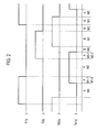
- Figure 2 is a timing chart illustrating operating waveforms of the switches in the auxiliary resonant commutated pole three-phase voltage inverter illustrated in Fig. 1 .
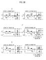
- Figure 3A is a mode transition diagram of the inverter illustrated in Fig. 1 from mode M0 of state A to mode M2 of state A.
- Figure 3B is a mode transition diagram of the same from mode M3-1 of state A to mode M3 of state B.
- S1g is a gate signal applied to a gate of the switch S1
- S2g is a gate signal applied to a gate of the switch S2
- Sa1g is a gate signal applied to a gate of the switch Sa1
- Sa2g is a gate signal applied to a gate of the switch Sa2.
- the gate signal Sa1g turns on the switch Sa1 to divide a current from the load RL.
- a divided current portion passes through the diode D1 to the DC power source Vdc and the other divided current portion passes through the reactor Lr, diode Da2, and switch Sa1, to accumulate power in the reactor Lr.
- the gate signal S1g turns off the switch S1 and the reactor Lr and capacitors Cr1 and Cr2 resonate. At this time, the capacitor Cr2 connected in parallel with the switch S2 is discharged and the capacitor Cr1 connected in parallel with the switch S1 is charged.
- mode M0 of state B a current from the load RL passes through the switch S2.
- the gate signal Sa2g turns on the switch Sa2, so that a current passing through a path extending along Da1, Sa2, and Lr from the left to the right together with a current of the load RL pass through the switch S2.
- the resonant power conversion apparatus contains the voltage dividing point between the capacitors C1 and C2, to divide a voltage of the DC power source Vdc. Potential at the voltage dividing point fluctuates depending on load conditions and temperature and this results in shortening the service life of the capacitors C1 and C2.
- the present invention provides a resonant power conversion apparatus capable of securing long service life and high reliability.
- the resonant power conversion apparatus includes a transformer having a primary winding, a secondary winding, a tertiary winding connected in series with the secondary winding, and a reset winding connected in series with the primary winding; a first series circuit connected between first and second ends of a DC power source and including a first switch and a second switch; a first capacitor and a first diode that are connected in parallel with the first switch; a second capacitor and a second diode that are connected in parallel with the second switch; a second series circuit connected between the first and second ends of the DC power source and including the primary winding of the transformer and a third diode; a third series circuit connected between the first and second ends of the DC power source and including the reset winding of the transformer and a fourth diode; a reactor connected between a connection point of the first and second switches and a connection point of the secondary and tertiary windings of the transformer; a first auxiliary switch connected between the first end of the
- FIG. 4 is a circuit diagram illustrating a resonant power conversion apparatus according to Embodiment 1 of the present invention.
- This apparatus is an auxiliary resonant commutated pole three-phase voltage inverter employing transformers and Fig. 4 illustrates a one-phase portion of the apparatus.
- the transformer T1 has a primary winding n1 a secondary winding n2, a tertiary winding n3 connected in series with the secondary winding n2, and a reset winding nR connected in series with the primary winding n1.
- the reset, primary, secondary, and tertiary windings nR, n1, n2, and n3 of the transformer T1 have a turn ratio of 2:2:1:1.
- Ends of a DC power source Vdc are connected to a first series circuit including a switch S1 (first switch) of an insulated gate bipolar transistor and a switch S2 (second switch) of an insulated gate bipolar transistor.
- the switch S1 has a collector and an emitter between which a capacitor Cr1 (first capacitor) and a diode D1 (first diode) are connected.
- the switch S2 has a collector and an emitter between which a capacitor Cr2 (second capacitor ) and a diode D2 (second diode) are connected.
- the ends of the DC power source Vdc are also connected to a second series circuit including the primary winding n1 of the transformer and a diode Dn1 (third diode), as well as to a third series circuit including the reset winding nR of the transformer T1 and a diode DR (fourth diode).
- a connection point "b" of the switches S1 andS2 and a connection point “a” of the secondary and tertiary windings n2 and n3 of the transformer T1 are connected to a reactor Lr.
- the connection point "b” of the switches S1 and S2 is connected to a load RL.
- a positive electrode of the DC power source Vdc and a first end of the secondary winding n2 of the transformer T1 are connected to a switch S10 (first auxiliary switch) that operates in a direction in which a current flows from a positive electrode line of the DC power source Vdc.
- the switch S10 includes a series circuit of a switch Sa1 (third switch) of an insulated gate bipolar transistor and a diode Da1 (fifth diode).
- a negative electrode of the DC power source Vdc and a first end of the tertiary winding n3 of the transformer T1 are connected to a switch S20 (second auxiliary switch) that operates in a direction in which a current flows from a negative electrode line of the DC power source Vdc.
- the switch S20 includes a series circuit of a switch Sa2 (fourth switch) made of an insulated gate bipolar transistor and a diode Da2 (sixth diode).
- the reset winding nR and diode DR form a reset circuit to discharge energy from an exciting inductance of the transformer T1.
- the reset circuit counter electromotive force generated by the exciting inductance of the transformer during an OFF period of the switch Sa1 or Sa2 is returned to the DC power source Vdc, thereby greatly reducing a voltage applied to the switches Sa1 and Sa2.
- a controller 10 alternately turns on the switches S1 and S2 and alternately turns on the switches Sa1 and Sa2. More precisely, before a period in which the switches S1 and S2 are both OFF, the controller 10 turns on one of the switches Sa1 and Sa2, to realize a zero-voltage switching operation of the switches S1 and S2 by achieving a resonance of the capacitors Cr1 and Cr2 and reactor Lr during the OFF period of the switches S1 and S2.
- Fig. 5 illustrates operating waveforms of the apparatus in states A and B
- Fig. 6 illustrates mode transition of the apparatus in states A and B.
- Fig. 6 only operating parts of the apparatus are illustrated with solid lines.
- S1g is a gate signal applied to a gate of the switch S1
- S2g is a gate signal applied to a gate of the switch S2
- Sa1g is a gate signal applied to a gate of the switch Sa1
- Sa2g is a gate signal applied to a gate of the switch Sa2
- Vdc is a voltage of the DC power source Vdc
- iLr is a current passing through the reactor Lr
- ix is a current of the load RL
- Vs1 is a collector-emitter voltage of the switch S1
- Vs2 is a collector-emitter voltage of the switch S2
- is1 is a current passing through the switch S1 or the diode D1
- is2 is a current passing through the switch S2 or the diode D2.
- the switch S1 In mode M0 of state A, the switch S1 is OFF and the switch S2 is ON.
- the current is2 (negative current) passes through the diode D2 to the load RL.
- the load current ix has a constant value.
- the gate signal Sa1g turns on the switch Sa1, to pass the current iLr through a path extending along Vdc, Sa1, Da1, n2, and Lr.
- the currents iLr and is 2 (negative current) pass through the load RL.
- a current passes counterclockwise through a path extending along n1, Vdc, Dn1, and n1.
- the primary winding n1 receives a voltage from the DC power source Vdc.
- the primary, secondary, and tertiary windings n1, n2, and n3 have a turn ratio of 2:1:1, and therefore, one half of the voltage of the DC power source Vdc is applied to the connection point "a" of the secondary and tertiary windings n2 and n3.
- the current iLr exceeds the current ix, and then, the current is2 (positive current), i.e., the difference between the current iLr and the current ix passes through the switch S2.
- the gate signal S2g turns off the switch S2 and the reactor Lr and capacitors Cr1 and Cr2 resonate. At this time, the capacitor Cr2 is charged and the capacitor Cr1 is discharged. This results in increasing the voltage Vs2 across the switch S2 and decreasing the voltage Vs1 across the switch S1.
- the gate signal Sa2g turns on the switch Sa2, to pass the current iLr through a path extending along S1, Lr, n3, Da2, and Sa2. This increases the current is1 passing through the switch S1. At this time, a current passes counterclockwise through a path extending along n1, Vdc, Dn1, and n1.
- the primary winding n1 receives the voltage of the DC power source Vdc.
- the primary, secondary, and tertiary windings n1, n2, and n3 have a turn ratio of 2:1:1, and therefore, one half of the DC power source voltage Vdc is applied to the connection point "a" of the secondary and tertiary windings n2 and n3.
- the gate signal S1g turns off the switch S1 and the reactor Lr and capacitors Cr1 and Cr2 resonate. At this time, the capacitor Cr1 is charged and the capacitor Cr2 is discharged. This results in increasing the voltage Vs1 across the switch S1 and decreasing the voltage Vs2 across the switch S2.
- the switch S2 In mode M0 of state C, the switch S2 is OFF and the switch S1 is ON.
- the diode D1 passes the current is1 that is the same as the current passing through the load RL.
- the load current ix has a constant value.
- the gate signal Sa2g turns on the switch Sa2 to pass the current iLr through the path extending along Lr, n3, Da2, and Sa2.
- the current ix is divided into the currents iLr and is2.
- a current passes counterclockwise through the path extending along n1, Vdc, Dn1, and n1.
- the primary winding n1 receives the DC power source voltage Vdc.
- the primary, secondary, and tertiary windings n1, n2, and n3 have a turn ratio of 2:1:1, and therefore, one half of the DC power source voltage Vdc is applied to the connection point "a" of the secondary and tertiary windings n2 and n3.
- the current iLr becomes larger than the current ix and the current is1 (positive current), which is obtained by subtracting the current ix from the current iLr, passes through the switch S1.
- the gate signal S1g turns off the switch S1 and the reactor Lr and capacitors Cr1 and Cr2 resonate. At this time, the capacitor Cr1 is charged and the capacitor Cr2 is discharged. This results in increasing the voltage Vs1 across the switch S1 and decreasing the voltage Vs2 across the switch S2.
- mode M3-1 of state C the voltage Vcr1 across the capacitor Cr1 becomes larger than the power source voltage Vdc and the diode D2 turns on to pass the current is2 through the diode D2.
- the gate signal S2g turns on the switch S2, thereby realizing the zero-voltage switching of the switch S2.
- mode M3-2 of state C the current iLr becomes smaller than the current ix and the current is2, which is obtained by subtracting the current iLr from the current ix, passes through the switch S2.
- the gate signal Sa1g turns on the switch Sa1 and the current iLr passes through a path extending along Sa1, Da1, n2, Lr, and S2, to increase the current is2 of the switch S2.
- a current passes counterclockwise through the path extending along n1, Vdc, Dn1, and n1.
- the primary winding n1 receives the DC power source voltage Vdc.
- the primary, secondary, and tertiary windings n1, n2, and n3 have a turn ratio of 2:1:1, and therefore, one half of the voltage of the DC power source Vdc is applied to the connection point "a" of the secondary and tertiary windings n2 and n3.
- the gate signal S2g turns off the switch S2 and the reactor Lr and capacitors Cr1 and Cr2 resonate. At this time, the capacitor Cr2 is charged and the capacitor Cr1 is discharged. This results in increasing the voltage Vs2 across the switch S2 and decreasing the voltage Vs1 across the switch S1.
- the resonant power conversion apparatus employs the transformer T1 instead of the two voltage dividing capacitors C1 and C2 of the related art illustrated in Fig. 1 , to achieve performance equivalent to that achieved with the capacitors of the related art.
- the primary, secondary, and tertiary windings n1, n2, and n3 of the transformer T1 have a turn ratio of 2:1:1, and therefore, one half of the DC voltage Vdc is applied to the connection point "a" of the secondary and tertiary windings n2 and n3.
- the exciting inductance of the transformer T1 produces counter electromotive force, which is returned to the DC power source Vdc through the diode DR and reset winding nR, to greatly reduce a voltage applied to the switches Sa1 and Sa2. This prevents the switches Sa1 and Sa2 from deteriorating or breaking, elongates the service life of the switches Sa1 and Sa2, and improves the reliability of the resonant power conversion apparatus.
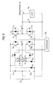
- FIG. 9 is a circuit diagram illustrating a resonant power conversion apparatus according to Embodiment 2 of the present invention. This is a half-bridge resonant power conversion apparatus. Compared with Embodiment 1 illustrated in Fig. 4 , Embodiment 2 additionally employs capacitors C10 and C20, a reactor Lf, and a capacitor Cf.
- Both ends of a DC power source Vdc are connected to a series circuit including the capacitors C10 and C20.
- a series circuit (a harmonics removing filter circuit) including the reactor Lf and capacitor Cf.
- Both ends of the capacitor Cf are connected to a load RL, to provide the load RL with single-phase sinusoidal AC power.
- Effect of Embodiment 2 is similar to that of Embodiment 1.
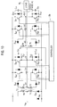
- FIG 10 is a circuit diagram illustrating a resonant power conversion apparatus according to Embodiment 3 of the present invention.
- Embodiment 3 employs a single-phase, full-bridge configuration with respect to Embodiment 2 that employs a half-bridge configuration as illustrated in Fig. 9 .
- the resonant power conversion apparatus of Embodiment 3 includes a transformer T2 provided with a primary winding n1, secondary windings n2 and n4, tertiary windings n3 and n5, and a reset winding nR and diodes DR and Dn1.
- the apparatus of Embodiment 3 employs, for U-phase, switches SU1, SU2, Sa1 and Sa2, diodes Da1 and Da2, capacitors Cr1 and Cr2, and a reactor Lr1, and for V-phase, switches SV1, SV2, Sa3, and Sa4, diodes Da3 and Da4, capacitors Cr3 and Cr4, and a reactor Lr2.
- a controller 10b has the same function as the controller 10 of Embodiment 1 and controls ON/OFF of the switches SU1, SU2, Sa1 and Sa2 and the switches SV1, SV2, Sa3, and Sa4.
- FIG 11 is a circuit diagram illustrating a resonant power conversion apparatus according to Embodiment 4 of the present invention.
- Embodiment 4 employs a three-phase, full-bridge configuration with respect to Embodiment 1 that employs a one-phase configuration as illustrated in Fig. 4 .
- the resonant power conversion apparatus of Embodiment 4 includes a transformer T3 provided with a primary winding n1, secondary windings n2, n4, and n6, tertiary windings n3, n5, and n7, and a reset winding nR and diodes DR and Dn1.
- the apparatus of Embodiment 4 includes, for U-phase, switches SU1, SU2, Sa1, and Sa2, diodes Da1 and Da2, capacitors Cr1 and Cr2, and a reactor Lr1, for V-phase, switches SV1, SV2, Sa3, and Sa4, diodes Da3 and Da4, capacitors Cr3 and Cr4, and a reactor Lr2, and for W-phase, switches SW1, SW2, Sa5, and Sa6, diodes Da5 and Da6, capacitors Cr5 and Cr6, and a reactor Lr3.
- a controller 10c has the same function as the controller 10 of Embodiment 1 and controls ON/OFF of the switches SU1, SU2, Sa1, and Sa2, switches SV1, SV2, Sa3, and Sa4, and switches SW1, SW2, Sa5, and Sa6.
- the present invention is not limited to the resonant power conversion apparatuses of Embodiments 1 to 4.
- the gate signal Sa1g to the switch Sa1 is ON in modes M1, M2, and M3 of state A and modes M1, M2, and M3 of state D and the gate signal Sa2g to the switch Sa2 is ON in modes M1, M2, and M3 of state B and modes M1, M2, and M3 of state C.
- the gate signal Sa1g to the switch Sa1 may be ON in modes M1, M2, and M3 of state A, mode M0 of state B, modes M1, M2, and M3 of state D, and mode M0 of state C and the gate signal Sa2g to the switch Sa2 is ON in modes M1, M2, M3 of state B, mode M0 of state A, modes M1, M2, and M3 of state C, and mode M0 of state D.
- This configuration may provides an effect similar to that of Embodiment 1.
- the resonant power conversion apparatus employs a transformer instead of two voltage dividing capacitors, to realize performance equivalent to that realized by the capacitors. Even if the exciting inductance of the transformer produces counter electromotive force during an OFF period of the first or second auxiliary switch, the present invention returns the counter electromotive force to a DC power source through the fourth diode and reset winding, to greatly reduce a voltage applied to the first and second auxiliary switches.
- the resonant power conversion apparatus according to the present invention therefore, has long service life and high reliability.
- the present invention is applicable to, for example, inverters for electric vehicles.
Landscapes
- Engineering & Computer Science (AREA)
- Power Engineering (AREA)
- Inverter Devices (AREA)
- Dc-Dc Converters (AREA)
Abstract
Description
- The present invention relates to a resonant power conversion apparatus applicable to, for example, a hybrid vehicle inverter and an electric vehicle inverter.
- Among power conversion apparatuses, the resonant power conversion apparatus is known to be capable of reducing a switching loss. A typical example of the resonant power conversion apparatus is an auxiliary resonant commutated pole three-phase voltage inverter that reduces a switching loss by soft-switching switches through an auxiliary resonant circuit that performs resonant operation.
-
Figure 1 is a circuit diagram illustrating a one-phase portion of an auxiliary resonant commutated pole three-phase voltage inverter according to a related art disclosed in Japanese Unexamined Patent Application Publication No.H08-340676 Fig. 1 , both ends of a DC power source Vdc are connected to a series circuit including capacitors C1 and C2 having the same capacitance. A connection point of the capacitors C1 and C2 generates a voltage that is half a voltage of the DC power source Vdc. - Switches S1 and S2 are insulated gate bipolar transistors (IGBTs) and are connected in series. Both ends of the series circuit of the switches S1 and S2 are connected to the ends of the DC power source Vdc. The switch S1 has a collector and an emitter between which a capacitor Cr1 and a diode D1 are connected. The switch S2 has a collector and an emitter between which a capacitor Cr2 and a diode D2 are connected. A connection point of the switches S1 and S2 is connected to a load RL.
- Connected between the connection point of the switches S1 and S2 and the connection point of the capacitors C1 and C2 is a series circuit including a reactor Lr and switches Sa1 and Sa2. The switches S1a and Sa2 form an auxiliary resonant circuit and are connected to diodes Da1 and Da2, respectively.
- The switches S1 and S2 carry out a zero-voltage, zero-current turn-ON operation with a resonant current provided by the auxiliary resonant circuit, to greatly reduce a switching loss.
-
Figure 2 is a timing chart illustrating operating waveforms of the switches in the auxiliary resonant commutated pole three-phase voltage inverter illustrated inFig. 1 .Figure 3A is a mode transition diagram of the inverter illustrated inFig. 1 from mode M0 of state A to mode M2 of state A.Figure 3B is a mode transition diagram of the same from mode M3-1 of state A to mode M3 of state B. - In
Fig. 2 , S1g is a gate signal applied to a gate of the switch S1, S2g is a gate signal applied to a gate of the switch S2, Sa1g is a gate signal applied to a gate of the switch Sa1, and Sa2g is a gate signal applied to a gate of the switch Sa2. - Operation of the resonant power conversion apparatus of
Fig. 1 will be explained with reference toFigs. 2 to 3B . In mode M0 of state A, the switch S1 is ON and the diode D1 turns on to pass a current through a path extending along the load RL, the diode D1, and the DC power source Vdc. - In mode M1-1 of state A, the gate signal Sa1g turns on the switch Sa1 to divide a current from the load RL. A divided current portion passes through the diode D1 to the DC power source Vdc and the other divided current portion passes through the reactor Lr, diode Da2, and switch Sa1, to accumulate power in the reactor Lr.
- In mode M1-2 of state A, a current of the switch S1 and a current of the load RL (each arrowed) pass through the reactor Lr, diode Da2, and switch Sa1, to accumulate power in the reactor Lr.
- In mode M2 of state A, the gate signal S1g turns off the switch S1 and the reactor Lr and capacitors Cr1 and Cr2 resonate. At this time, the capacitor Cr2 connected in parallel with the switch S2 is discharged and the capacitor Cr1 connected in parallel with the switch S1 is charged.
- In modes M3-1 and M3-2 of state A, the capacitor Cr2 completes the discharge and the diode D2 passes a current. When a drain-source voltage of the switch S2 is zero, the gate signal S2g turns on the switch S2, to realize the zero-voltage switching of the switch S2.
- In mode M0 of state B, a current from the load RL passes through the switch S2. In mode M1 of state B, the gate signal Sa2g turns on the switch Sa2, so that a current passing through a path extending along Da1, Sa2, and Lr from the left to the right together with a current of the load RL pass through the switch S2.
- In mode M2 of state B, the gate signal S2g turns off the switch S2. Then, the reactor Lr and capacitors Cr1 and Cr2 resonate. At this time, the capacitor Cr1 connected in parallel with the switch S1 is discharged and the capacitor Cr2 connected in parallel with the switch S2 is charged.
- Inmode M3 of state B, the capacitor Cr1 completes the discharge and the diode D1 passes a current. When a drain-source voltage of the switch S1 is zero, the switch S1 is turned on, to realize the zero-voltage switching of the switch S1.
- The resonant power conversion apparatus according to the related art of
Fig. 1 , however, contains the voltage dividing point between the capacitors C1 and C2, to divide a voltage of the DC power source Vdc. Potential at the voltage dividing point fluctuates depending on load conditions and temperature and this results in shortening the service life of the capacitors C1 and C2. - The present invention provides a resonant power conversion apparatus capable of securing long service life and high reliability.
- According to an aspect of the present invention, the resonant power conversion apparatus includes a transformer having a primary winding, a secondary winding, a tertiary winding connected in series with the secondary winding, and a reset winding connected in series with the primary winding; a first series circuit connected between first and second ends of a DC power source and including a first switch and a second switch; a first capacitor and a first diode that are connected in parallel with the first switch; a second capacitor and a second diode that are connected in parallel with the second switch; a second series circuit connected between the first and second ends of the DC power source and including the primary winding of the transformer and a third diode; a third series circuit connected between the first and second ends of the DC power source and including the reset winding of the transformer and a fourth diode; a reactor connected between a connection point of the first and second switches and a connection point of the secondary and tertiary windings of the transformer; a first auxiliary switch connected between the first end of the DC power source and a first end of the secondary winding of the transformer; a second auxiliary switch connected between the second end of the DC power source and a first end of the tertiary winding of the transformer; and a controller configured to alternately turn on the first and second switches and alternately turn on the first and second auxiliary switches, so that the first and second switches each conduct a zero-voltage switching operation.
-
-
Figure 1 is a circuit diagram illustrating a one-phase portion of an auxiliary resonant commutated pole three-phase voltage inverter according to a related art; -
Fig. 2 is a timing chart illustrating operating waveforms of switches in the inverter ofFig. 1 ; -
Fig. 3A is a mode transition diagram illustrating mode M0 of state A to mode M2 of state A of the inverter ofFig. 1 ; -
Fig. 3B is a mode transition diagram illustrating mode M3-1 of state A to mode M3 of state B of the inverter ofFig. 1 ; -
Fig. 4 is a circuit diagram illustrating a resonant power conversion apparatus according toEmbodiment 1 of the present invention; -
Fig. 5 is a timing chart illustrating operating waveforms in states A and B ofEmbodiment 1; -
Fig. 6 is a mode transition diagram illustrating states A and B ofEmbodiment 1; -
Fig. 7 is a timing chart illustrating operating waveforms in states C and D ofEmbodiment 1; -
Fig. 8 is a mode transition diagram illustrating states C and D ofEmbodiment 1; -
Fig. 9 is a circuit diagram illustrating a resonant power conversion apparatus according toEmbodiment 2 of the present invention; -
Fig. 10 is a circuit diagram illustrating a resonant power conversion apparatus according to Embodiment 3 of the present invention; and -
Fig. 11 is a circuit diagram illustrating a resonant power conversion apparatus according to Embodiment 4 of the present invention. - Resonant power conversion apparatuses according to embodiments of the present invention will be explained in detail with reference to the drawings.
-
Figure 4 is a circuit diagram illustrating a resonant power conversion apparatus according toEmbodiment 1 of the present invention. This apparatus is an auxiliary resonant commutated pole three-phase voltage inverter employing transformers andFig. 4 illustrates a one-phase portion of the apparatus. - In
Fig. 4 , the transformer T1 has a primary winding n1 a secondary winding n2, a tertiary winding n3 connected in series with the secondary winding n2, and a reset winding nR connected in series with the primary winding n1. The reset, primary, secondary, and tertiary windings nR, n1, n2, and n3 of the transformer T1 have a turn ratio of 2:2:1:1. - Ends of a DC power source Vdc are connected to a first series circuit including a switch S1 (first switch) of an insulated gate bipolar transistor and a switch S2 (second switch) of an insulated gate bipolar transistor.
- The switch S1 has a collector and an emitter between which a capacitor Cr1 (first capacitor) and a diode D1 (first diode) are connected. The switch S2 has a collector and an emitter between which a capacitor Cr2 (second capacitor ) and a diode D2 (second diode) are connected.
- The ends of the DC power source Vdc are also connected to a second series circuit including the primary winding n1 of the transformer and a diode Dn1 (third diode), as well as to a third series circuit including the reset winding nR of the transformer T1 and a diode DR (fourth diode).
- A connection point "b" of the switches S1 andS2 and a connection point "a" of the secondary and tertiary windings n2 and n3 of the transformer T1 are connected to a reactor Lr. The connection point "b" of the switches S1 and S2 is connected to a load RL.
- A positive electrode of the DC power source Vdc and a first end of the secondary winding n2 of the transformer T1 are connected to a switch S10 (first auxiliary switch) that operates in a direction in which a current flows from a positive electrode line of the DC power source Vdc. The switch S10 includes a series circuit of a switch Sa1 (third switch) of an insulated gate bipolar transistor and a diode Da1 (fifth diode).
- A negative electrode of the DC power source Vdc and a first end of the tertiary winding n3 of the transformer T1 are connected to a switch S20 (second auxiliary switch) that operates in a direction in which a current flows from a negative electrode line of the DC power source Vdc. The switch S20 includes a series circuit of a switch Sa2 (fourth switch) made of an insulated gate bipolar transistor and a diode Da2 (sixth diode).
- The reset winding nR and diode DR form a reset circuit to discharge energy from an exciting inductance of the transformer T1. With the reset circuit, counter electromotive force generated by the exciting inductance of the transformer during an OFF period of the switch Sa1 or Sa2 is returned to the DC power source Vdc, thereby greatly reducing a voltage applied to the switches Sa1 and Sa2.
- A
controller 10 alternately turns on the switches S1 and S2 and alternately turns on the switches Sa1 and Sa2. More precisely, before a period in which the switches S1 and S2 are both OFF, thecontroller 10 turns on one of the switches Sa1 and Sa2, to realize a zero-voltage switching operation of the switches S1 and S2 by achieving a resonance of the capacitors Cr1 and Cr2 and reactor Lr during the OFF period of the switches S1 and S2. - Operation of the resonant power conversion apparatus according to
Embodiment 1 will be explained with reference toFigs. 5 and6 in whichFig. 5 illustrates operating waveforms of the apparatus in states A and B andFig. 6 illustrates mode transition of the apparatus in states A and B. InFig. 6 , only operating parts of the apparatus are illustrated with solid lines. - In
Fig. 5 , S1g is a gate signal applied to a gate of the switch S1, S2g is a gate signal applied to a gate of the switch S2, Sa1g is a gate signal applied to a gate of the switch Sa1, Sa2g is a gate signal applied to a gate of the switch Sa2, Vdc is a voltage of the DC power source Vdc, iLr is a current passing through the reactor Lr, ix is a current of the load RL, Vs1 is a collector-emitter voltage of the switch S1, Vs2 is a collector-emitter voltage of the switch S2, is1 is a current passing through the switch S1 or the diode D1, is2 is a current passing through the switch S2 or the diode D2. - In mode M0 of state A, the switch S1 is OFF and the switch S2 is ON. The current is2 (negative current) passes through the diode D2 to the load RL. The load current ix has a constant value.
- In mode M1-1 of state A, the gate signal Sa1g turns on the switch Sa1, to pass the current iLr through a path extending along Vdc, Sa1, Da1, n2, and Lr. The currents iLr and is 2 (negative current) pass through the load RL. At this time, a current passes counterclockwise through a path extending along n1, Vdc, Dn1, and n1. The primary winding n1 receives a voltage from the DC power source Vdc. The primary, secondary, and tertiary windings n1, n2, and n3 have a turn ratio of 2:1:1, and therefore, one half of the voltage of the DC power source Vdc is applied to the connection point "a" of the secondary and tertiary windings n2 and n3. In mode M1-2 of state A, the current iLr exceeds the current ix, and then, the current is2 (positive current), i.e., the difference between the current iLr and the current ix passes through the switch S2.
- In mode M2 of state A, the gate signal S2g turns off the switch S2 and the reactor Lr and capacitors Cr1 and Cr2 resonate. At this time, the capacitor Cr2 is charged and the capacitor Cr1 is discharged. This results in increasing the voltage Vs2 across the switch S2 and decreasing the voltage Vs1 across the switch S1.
- In mode M3-1 of state A, a voltage Vcr2 across the capacitor Cr2 becomes larger than the voltage Vdc, and then, the diode D1 turns on to pass the current is1 (negative current). At this time, the gate signal S1g turns on the switch S1, thereby realizing the zero-voltage switching of the switch S1. In mode M3-2 of state A, the current iLr becomes smaller than the current ix, and then, the current is1 (positive current), which is obtained by subtracting the current iLr from the current ix, passes through the switch S1.
- In mode M0 of state B, the current iLr becomes zero. The gate signal Sa1g turns off the switch Sa1 and only the current is1 passes through the load RL. When the switch Sa1 turns off, the exciting inductance of the transformer T1 produces counter electromotive force, which is returned to the DC power source Vdc through the diode DR and reset winding nR, to greatly reduce a voltage applied to the switch Sa1.
- In mode M1 of state B, the gate signal Sa2g turns on the switch Sa2, to pass the current iLr through a path extending along S1, Lr, n3, Da2, and Sa2. This increases the current is1 passing through the switch S1. At this time, a current passes counterclockwise through a path extending along n1, Vdc, Dn1, and n1. The primary winding n1 receives the voltage of the DC power source Vdc. The primary, secondary, and tertiary windings n1, n2, and n3 have a turn ratio of 2:1:1, and therefore, one half of the DC power source voltage Vdc is applied to the connection point "a" of the secondary and tertiary windings n2 and n3.
- In mode M2 of state B, the gate signal S1g turns off the switch S1 and the reactor Lr and capacitors Cr1 and Cr2 resonate. At this time, the capacitor Cr1 is charged and the capacitor Cr2 is discharged. This results in increasing the voltage Vs1 across the switch S1 and decreasing the voltage Vs2 across the switch S2.
- In mode M3 of state B, a voltage Vcr1 across the capacitor Cr1 becomes larger than the DC power source voltage Vdc and the diode D2 turns on to pass the current is2 (negative current). The gate signal S2g turns on the switch S2 to pass the current is2. In mode M0 of state A, the current iLr becomes zero and the gate signal Sa2g turns off the switch Sa2, so that only the current is2 passes through the load RL. When the switch Sa2 turns off, the exciting inductance of the transformer T1 produces counter electromotive force, which is returned to the DC power source Vdc through the diode DR and reset winding nR, to greatly reduce a voltage applied to the switch Sa2.
- Operation of the resonant power conversion apparatus of
Embodiment 1 in states C and D will be explained in detail with reference to operating waveforms illustrated inFig. 7 and a mode transition diagram illustrated inFig. 8 . InFig. 8 , only operating parts of the apparatus are illustrated with solid lines. - In mode M0 of state C, the switch S2 is OFF and the switch S1 is ON. The diode D1 passes the current is1 that is the same as the current passing through the load RL. The load current ix has a constant value.
- In mode M1-1 of state C, the gate signal Sa2g turns on the switch Sa2 to pass the current iLr through the path extending along Lr, n3, Da2, and Sa2. The current ix is divided into the currents iLr and is2. At this time, a current passes counterclockwise through the path extending along n1, Vdc, Dn1, and n1. The primary winding n1 receives the DC power source voltage Vdc. The primary, secondary, and tertiary windings n1, n2, and n3 have a turn ratio of 2:1:1, and therefore, one half of the DC power source voltage Vdc is applied to the connection point "a" of the secondary and tertiary windings n2 and n3. In mode M1-2 of state C, the current iLr becomes larger than the current ix and the current is1 (positive current), which is obtained by subtracting the current ix from the current iLr, passes through the switch S1.
- In mode M2 of state C, the gate signal S1g turns off the switch S1 and the reactor Lr and capacitors Cr1 and Cr2 resonate. At this time, the capacitor Cr1 is charged and the capacitor Cr2 is discharged. This results in increasing the voltage Vs1 across the switch S1 and decreasing the voltage Vs2 across the switch S2.
- In mode M3-1 of state C, the voltage Vcr1 across the capacitor Cr1 becomes larger than the power source voltage Vdc and the diode D2 turns on to pass the current is2 through the diode D2. At this time, the gate signal S2g turns on the switch S2, thereby realizing the zero-voltage switching of the switch S2. In mode M3-2 of state C, the current iLr becomes smaller than the current ix and the current is2, which is obtained by subtracting the current iLr from the current ix, passes through the switch S2.
- In mode M0 of state D, the current iLr becomes zero and the gate signal Sa2g turns off the switch Sa2, so that only the current is2 passes through the load RL. When the switch Sa2 turns off, the exciting inductance of the transformer T1 produces counter electromotive force, which is returned to the DC power source Vdc through the diode DR and reset winding nR, to greatly reduce a voltage applied to the switch Sa2.
- In mode M1 of state D, the gate signal Sa1g turns on the switch Sa1 and the current iLr passes through a path extending along Sa1, Da1, n2, Lr, and S2, to increase the current is2 of the switch S2. At this time, a current passes counterclockwise through the path extending along n1, Vdc, Dn1, and n1. The primary winding n1 receives the DC power source voltage Vdc. The primary, secondary, and tertiary windings n1, n2, and n3 have a turn ratio of 2:1:1, and therefore, one half of the voltage of the DC power source Vdc is applied to the connection point "a" of the secondary and tertiary windings n2 and n3.
- In mode M2 of state D, the gate signal S2g turns off the switch S2 and the reactor Lr and capacitors Cr1 and Cr2 resonate. At this time, the capacitor Cr2 is charged and the capacitor Cr1 is discharged. This results in increasing the voltage Vs2 across the switch S2 and decreasing the voltage Vs1 across the switch S1.
- In mode M3 of state D, the voltage Vcr2 across the capacitor Cr2 becomes larger than the voltage Vdc and the diode D1 turns on to pass the current is1. The gate signal S1g turns on the switch S1, to pass the current is1. In mode M0 of state C, the current iLr becomes zero. The gate signal Sa1g turns off the switch Sa1 and only the current is1 passes through the load RL. When the switch Sa1 turns off, the exciting inductance of the transformer T1 produces counter electromotive force, which is returned to the DC power source Vdc through the diode DR and reset winding nR, to greatly reduce a voltage applied to the switch Sa1.
- As mentioned above, the resonant power conversion apparatus according to
Embodiment 1 employs the transformer T1 instead of the two voltage dividing capacitors C1 and C2 of the related art illustrated inFig. 1 , to achieve performance equivalent to that achieved with the capacitors of the related art. According toEmbodiment 1, the primary, secondary, and tertiary windings n1, n2, and n3 of the transformer T1 have a turn ratio of 2:1:1, and therefore, one half of the DC voltage Vdc is applied to the connection point "a" of the secondary and tertiary windings n2 and n3. - When one of the switches Sa1 and Sa2 is OFF, the exciting inductance of the transformer T1 produces counter electromotive force, which is returned to the DC power source Vdc through the diode DR and reset winding nR, to greatly reduce a voltage applied to the switches Sa1 and Sa2. This prevents the switches Sa1 and Sa2 from deteriorating or breaking, elongates the service life of the switches Sa1 and Sa2, and improves the reliability of the resonant power conversion apparatus.
- If there is no diode DR nor reset winding nR, the counter electromotive force produced by the exciting inductance of the transformer T1 during an OFF period of any one of the switches Sa1 and Sa2 causes the secondary and tertiary windings n2 and n3 to generate voltages. These voltages are surge voltages applied to the switches Sa1 and Sa2, to break the switches Sa1 and Sa2. This problem never occurs in the resonant power conversion apparatus of
Embodiment 1. -
Figure 9 is a circuit diagram illustrating a resonant power conversion apparatus according toEmbodiment 2 of the present invention. This is a half-bridge resonant power conversion apparatus. Compared withEmbodiment 1 illustrated inFig. 4 ,Embodiment 2 additionally employs capacitors C10 and C20, a reactor Lf, and a capacitor Cf. - Both ends of a DC power source Vdc are connected to a series circuit including the capacitors C10 and C20. Connected between a connection point of the capacitors C10 and C20 and a connection point "b'" of switches S1 and S2 is a series circuit (a harmonics removing filter circuit) including the reactor Lf and capacitor Cf. Both ends of the capacitor Cf are connected to a load RL, to provide the load RL with single-phase sinusoidal AC power. Effect of
Embodiment 2 is similar to that ofEmbodiment 1. -
Figure 10 is a circuit diagram illustrating a resonant power conversion apparatus according to Embodiment 3 of the present invention. Embodiment 3 employs a single-phase, full-bridge configuration with respect toEmbodiment 2 that employs a half-bridge configuration as illustrated inFig. 9 . - Namely, the resonant power conversion apparatus of Embodiment 3 includes a transformer T2 provided with a primary winding n1, secondary windings n2 and n4, tertiary windings n3 and n5, and a reset winding nR and diodes DR and Dn1. In addition, the apparatus of Embodiment 3 employs, for U-phase, switches SU1, SU2, Sa1 and Sa2, diodes Da1 and Da2, capacitors Cr1 and Cr2, and a reactor Lr1, and for V-phase, switches SV1, SV2, Sa3, and Sa4, diodes Da3 and Da4, capacitors Cr3 and Cr4, and a reactor Lr2.
- A
controller 10b has the same function as thecontroller 10 ofEmbodiment 1 and controls ON/OFF of the switches SU1, SU2, Sa1 and Sa2 and the switches SV1, SV2, Sa3, and Sa4. - Effect of Embodiment 3 is similar to that of
Embodiment 1. -
Figure 11 is a circuit diagram illustrating a resonant power conversion apparatus according to Embodiment 4 of the present invention. Embodiment 4 employs a three-phase, full-bridge configuration with respect toEmbodiment 1 that employs a one-phase configuration as illustrated inFig. 4 . - Namely, the resonant power conversion apparatus of Embodiment 4 includes a transformer T3 provided with a primary winding n1, secondary windings n2, n4, and n6, tertiary windings n3, n5, and n7, and a reset winding nR and diodes DR and Dn1. In addition, the apparatus of Embodiment 4 includes, for U-phase, switches SU1, SU2, Sa1, and Sa2, diodes Da1 and Da2, capacitors Cr1 and Cr2, and a reactor Lr1, for V-phase, switches SV1, SV2, Sa3, and Sa4, diodes Da3 and Da4, capacitors Cr3 and Cr4, and a reactor Lr2, and for W-phase, switches SW1, SW2, Sa5, and Sa6, diodes Da5 and Da6, capacitors Cr5 and Cr6, and a reactor Lr3.
- A
controller 10c has the same function as thecontroller 10 ofEmbodiment 1 and controls ON/OFF of the switches SU1, SU2, Sa1, and Sa2, switches SV1, SV2, Sa3, and Sa4, and switches SW1, SW2, Sa5, and Sa6. - Effect of Embodiment 4 is similar to that of
Embodiment 1. - The present invention is not limited to the resonant power conversion apparatuses of
Embodiments 1 to 4. According toEmbodiment 1, the gate signal Sa1g to the switch Sa1 is ON in modes M1, M2, and M3 of state A and modes M1, M2, and M3 of state D and the gate signal Sa2g to the switch Sa2 is ON in modes M1, M2, and M3 of state B and modes M1, M2, and M3 of state C. Instead, the gate signal Sa1g to the switch Sa1 may be ON in modes M1, M2, and M3 of state A, mode M0 of state B, modes M1, M2, and M3 of state D, and mode M0 of state C and the gate signal Sa2g to the switch Sa2 is ON in modes M1, M2, M3 of state B, mode M0 of state A, modes M1, M2, and M3 of state C, and mode M0 of state D. This configuration may provides an effect similar to that ofEmbodiment 1. - As mentioned above, the resonant power conversion apparatus according to the present invention employs a transformer instead of two voltage dividing capacitors, to realize performance equivalent to that realized by the capacitors. Even if the exciting inductance of the transformer produces counter electromotive force during an OFF period of the first or second auxiliary switch, the present invention returns the counter electromotive force to a DC power source through the fourth diode and reset winding, to greatly reduce a voltage applied to the first and second auxiliary switches. The resonant power conversion apparatus according to the present invention, therefore, has long service life and high reliability.
- The present invention is applicable to, for example, inverters for electric vehicles.
- Although the invention has been described above by reference to certain embodiments of the invention, the invention is not limited to the embodiments described above. Modifications and variations of the embodiments described above will occur to those skilled in the art, in light of the teachings. The scope of the invention is defined with reference to the following claims.
Claims (4)
- A resonant power conversion apparatus comprising:a transformer having a primary winding, a secondary winding, a tertiary winding connected in series with the secondary winding, and a reset winding connected in series with the primary winding;a first series circuit connected between first and second ends of a DC power source and including a first switch and a second switch;a first capacitor and a first diode that are connected in parallel with the first switch;a second capacitor and a second diode that are connected in parallel with the second switch;a second series circuit connected between the first and second ends of the DC power source and including the primary winding of the transformer and a third diode;a third series circuit connected between the first and second ends of the DC power source and including the reset winding of the transformer and a fourth diode;a reactor connected between a connection point of the first and second switches and a connection point of the secondary and tertiary windings of the transformer;a first auxiliary switch connected between the first end of the DC power source and a first end of the secondary winding of the transformer;a second auxiliary switch connected between the second end of the DC power source and a first end of the tertiary winding of the transformer; anda controller configured to alternately turn on the first and second switches and alternately turn on the first and second auxiliary switches, so that the first and second switches each conduct a zero-voltage switching operation.
- The resonant power conversion apparatus of claim 1, wherein:the first auxiliary switch is a series circuit including a third switch and a fifth diode that are connected in series; andthe second auxiliary switch is a series circuit including a fourth switch and a sixth diode that are connected in series.
- The resonant power conversion apparatus of claim 1 or claim 2, wherein
the reset, primary, secondary, and tertiary windings of the transformer have a turn ratio of 2:2:1:1. - The resonant power conversion apparatus of any one of claims 1 to 3, wherein
the resonant power conversion apparatus employs a configuration selected from the group containing a half-bridge configuration, a single-phase, full-bridge configuration, and a three-phase, full-bridge configuration, to supply AC power to a load.
Applications Claiming Priority (1)
| Application Number | Priority Date | Filing Date | Title |
|---|---|---|---|
| JP2009199505A JP5388762B2 (en) | 2009-08-31 | 2009-08-31 | Resonant power converter |
Publications (2)
| Publication Number | Publication Date |
|---|---|
| EP2290798A1 true EP2290798A1 (en) | 2011-03-02 |
| EP2290798B1 EP2290798B1 (en) | 2013-10-09 |
Family
ID=42985532
Family Applications (1)
| Application Number | Title | Priority Date | Filing Date |
|---|---|---|---|
| EP20100173638 Not-in-force EP2290798B1 (en) | 2009-08-31 | 2010-08-23 | Resonant power converter |
Country Status (3)
| Country | Link |
|---|---|
| US (1) | US8300428B2 (en) |
| EP (1) | EP2290798B1 (en) |
| JP (1) | JP5388762B2 (en) |
Cited By (1)
| Publication number | Priority date | Publication date | Assignee | Title |
|---|---|---|---|---|
| CN112398359A (en) * | 2020-11-09 | 2021-02-23 | 国创新能源汽车智慧能源装备创新中心(江苏)有限公司 | Control circuit and control method of auxiliary resonance converter pole converter |
Families Citing this family (9)
| Publication number | Priority date | Publication date | Assignee | Title |
|---|---|---|---|---|
| EP2800265A1 (en) * | 2013-05-03 | 2014-11-05 | ALSTOM Technology Ltd | Converter |
| JP6999387B2 (en) * | 2017-12-04 | 2022-01-18 | ローム株式会社 | Power converter |
| JP7144591B2 (en) * | 2017-12-04 | 2022-09-29 | ローム株式会社 | power converter |
| JP7062565B2 (en) * | 2018-02-23 | 2022-05-06 | ニチコン株式会社 | Bidirectional DC / DC converter |
| JP7156938B2 (en) * | 2018-12-28 | 2022-10-19 | ニチコン株式会社 | Bidirectional inverter and power storage system provided with the bidirectional inverter |
| CN111490698B (en) * | 2020-04-16 | 2022-03-18 | 山西大学 | An Auxiliary Resonant Commutated Pole Inverter with Phase-dependent ZVT Magnetization Current Minimization |
| JP7577620B2 (en) * | 2021-06-28 | 2024-11-05 | ニチコン株式会社 | DC-DC converter with auxiliary resonant circuit |
| CA3245366A1 (en) * | 2022-03-03 | 2023-09-14 | Hillcrest Energy Technologies Ltd. | Auxiliary resonant commutated pole converter with self voltage balancing capability |
| JP7704191B1 (en) * | 2023-12-28 | 2025-07-08 | 株式会社明電舎 | Power Converter |
Citations (2)
| Publication number | Priority date | Publication date | Assignee | Title |
|---|---|---|---|---|
| JPH08340676A (en) | 1995-06-14 | 1996-12-24 | Toshiba Corp | Resonant power converter control method and controller thereof |
| EP1037369A2 (en) * | 1999-03-10 | 2000-09-20 | Kansai Research Institute (KRI) | Electric power generating system |
Family Cites Families (21)
| Publication number | Priority date | Publication date | Assignee | Title |
|---|---|---|---|---|
| US4365171A (en) * | 1980-12-23 | 1982-12-21 | General Electric Company | Low loss snubber circuit |
| US4785387A (en) * | 1986-04-28 | 1988-11-15 | Virginia Tech Intellectual Properties, Inc. | Resonant converters with secondary-side resonance |
| US4857822A (en) * | 1987-09-23 | 1989-08-15 | Virginia Tech Intellectual Properties, Inc. | Zero-voltage-switched multi-resonant converters including the buck and forward type |
| JPH04125069A (en) * | 1990-09-17 | 1992-04-24 | Canon Inc | Power source device |
| US5521807A (en) * | 1992-12-31 | 1996-05-28 | Interpoint Corporation | DC-To-DC converter with secondary flyback core reset |
| US5303138A (en) * | 1993-04-29 | 1994-04-12 | At&T Bell Laboratories | Low loss synchronous rectifier for application to clamped-mode power converters |
| US5815380A (en) * | 1993-11-16 | 1998-09-29 | Optimum Power Conversion, Inc. | Switching converter with open-loop primary side regulation |
| JP3235711B2 (en) * | 1996-01-16 | 2001-12-04 | 新電元工業株式会社 | Switching power supply |
| US5886508A (en) * | 1997-08-29 | 1999-03-23 | Computer Products, Inc. | Multiple output voltages from a cascaded buck converter topology |
| US5963438A (en) * | 1998-04-13 | 1999-10-05 | Virginia Power Technologies, Inc. | Bi-directional magnetic isolator |
| JPH11299237A (en) * | 1998-04-16 | 1999-10-29 | Nippon Electric Ind Co Ltd | Forward converter with active clamping circuit |
| JP2000224863A (en) * | 1998-11-25 | 2000-08-11 | Sanken Electric Co Ltd | Inverter apparatus |
| JP3296424B2 (en) * | 1999-03-08 | 2002-07-02 | サンケン電気株式会社 | Power converter |
| US6304463B1 (en) * | 1999-05-07 | 2001-10-16 | Power-One, Inc. | Single-ended forward converter circuit with quasi-optimal resetting for synchronous rectification |
| US6317341B1 (en) * | 2000-11-09 | 2001-11-13 | Simon Fraidlin | Switching circuit, method of operation thereof and single stage power factor corrector employing the same |
| US6473318B1 (en) * | 2000-11-20 | 2002-10-29 | Koninklijke Philips Electronics N.V. | Leakage energy recovering system and method for flyback converter |
| US6621718B1 (en) * | 2000-11-22 | 2003-09-16 | International Business Machines Corporation | Resonant converter circuit |
| US6512352B2 (en) * | 2001-06-07 | 2003-01-28 | Koninklijke Philips Electronics N.V. | Active clamp step-down converter with power switch voltage clamping function |
| US6507174B1 (en) * | 2001-09-06 | 2003-01-14 | Koninklijke Philips Electronics N.V. | Voltage regulator with clamping circuit |
| US6760236B2 (en) * | 2002-09-04 | 2004-07-06 | Chih-Hung Hsieh | Third winding reset forward converter |
| US7095638B2 (en) * | 2003-09-03 | 2006-08-22 | Tyco Electronics Power Systems, Inc. | Controller for complementary switches of a power converter and method of operation thereof |
-
2009
- 2009-08-31 JP JP2009199505A patent/JP5388762B2/en not_active Expired - Fee Related
-
2010
- 2010-08-23 EP EP20100173638 patent/EP2290798B1/en not_active Not-in-force
- 2010-08-23 US US12/861,327 patent/US8300428B2/en not_active Expired - Fee Related
Patent Citations (2)
| Publication number | Priority date | Publication date | Assignee | Title |
|---|---|---|---|---|
| JPH08340676A (en) | 1995-06-14 | 1996-12-24 | Toshiba Corp | Resonant power converter control method and controller thereof |
| EP1037369A2 (en) * | 1999-03-10 | 2000-09-20 | Kansai Research Institute (KRI) | Electric power generating system |
Non-Patent Citations (4)
| Title |
|---|
| HERBST J D ET AL: "Experimental results and design guidelines derived from the testing of a 2 MW, 250 Hz, auxiliary resonant commutated pole bi-directional converter", APPLIED POWER ELECTRONICS CONFERENCE AND EXPOSITION, 2008. APEC 2008. TWENTY-THIRD ANNUAL IEEE, IEEE, PISCATAWAY, NJ, USA, 24 February 2008 (2008-02-24), pages 1240 - 1246, XP031253407, ISBN: 978-1-4244-1873-2 * |
| HISANORI MORII ET AL: "Capacitor-Less Auxiliary Resonant Commutated Pole (ARCP) voltage source soft switching inverter suitable for EV", POWER ELECTRONICS AND APPLICATIONS, 2009. EPE '09. 13TH EUROPEAN CONFERENCE ON, IEEE, PISCATAWAY, NJ, USA, 8 September 2009 (2009-09-08), pages 1 - 8, XP031541389, ISBN: 978-1-4244-4432-8 * |
| SALBERTA F R ET AL: "An improved control strategy for a 50-kHz auxiliary resonant commutated pole converter", IECEC '97. PROCEEDINGS OF THE 32ND INTERSOCIETY ENERGY CONVERSION ENGINEERING CONFERENCE. AEROSPACE POWER SYSTEMS AND TECHNOLOGIES. HONOLULU, HI, JULY 27 - AUG. 1, 1997; [INTERSOCIETY ENERGY CONVERSION ENGINEERING CONFERENCE], NEW YORK, NY : IEEE, US, vol. 1, 27 July 1997 (1997-07-27), pages 332 - 336, XP010269028, ISBN: 978-0-7803-4515-7 * |
| YOSHIDA M ET AL: "Active resonant leg-link snubber-assisted three phase soft commutation PFC converter and its practical evaluations", INDUSTRIAL ELECTRONICS SOCIETY, 2000. IECON 2000. 26TH ANNUAL CONFJERE NCE OF THE IEEE 22-28 OCT. 2000, PISCATAWAY, NJ, USA,IEEE, vol. 4, 22 October 2000 (2000-10-22), pages 2660 - 2665, XP010569213, ISBN: 978-0-7803-6456-1 * |
Cited By (1)
| Publication number | Priority date | Publication date | Assignee | Title |
|---|---|---|---|---|
| CN112398359A (en) * | 2020-11-09 | 2021-02-23 | 国创新能源汽车智慧能源装备创新中心(江苏)有限公司 | Control circuit and control method of auxiliary resonance converter pole converter |
Also Published As
| Publication number | Publication date |
|---|---|
| JP2011055580A (en) | 2011-03-17 |
| US8300428B2 (en) | 2012-10-30 |
| US20110051474A1 (en) | 2011-03-03 |
| EP2290798B1 (en) | 2013-10-09 |
| JP5388762B2 (en) | 2014-01-15 |
Similar Documents
| Publication | Publication Date | Title |
|---|---|---|
| EP2290798B1 (en) | Resonant power converter | |
| US9520792B2 (en) | Staggered parallel three-level DC/DC converter and AC/DC converter | |
| US9431917B2 (en) | Switching power supply including a rectifier circuit having switching elements, and electric power converter | |
| CN105144561B (en) | DC/DC converters | |
| US10432101B2 (en) | Power conversion apparatus | |
| US20080205109A1 (en) | Energy distribution system for vehicle | |
| US8259469B2 (en) | Current ripple reduction power conversion circuits | |
| JP6343187B2 (en) | DC / DC converter control device and control method thereof | |
| JP2015181329A (en) | Power converter | |
| US11728747B2 (en) | Soft switched voltage source inverter | |
| US8665616B2 (en) | Near zero current-ripple inversion or rectification circuits | |
| JP6467524B2 (en) | Power converter and railway vehicle | |
| Bolte et al. | Bidirectional resonant converter with integrated magnetics for on-board chargers | |
| US11990850B2 (en) | Soft switched voltage source inverter | |
| JP2020022307A (en) | Power supply device and method of controlling the same | |
| JP2015122903A (en) | Switching power-supply device and power conversion device | |
| JP5749853B2 (en) | Power converter | |
| TWI407669B (en) | Power converter with low current ripple | |
| Oh et al. | Light-Load Efficiency Enhancement of Soft-Switching Auxiliary Resonant Commutated Pole Inverter With Dual Active Modulation | |
| Yang et al. | Power efficiency improvement of dual-buck inverter with SiC diodes using coupled inductors | |
| JP2015139312A (en) | Switching power supply, power converter | |
| JP2008067427A (en) | Power conversion device | |
| US9281740B2 (en) | Power conversion apparatus | |
| JP2009147996A (en) | Power conversion circuit | |
| JP7144591B2 (en) | power converter |
Legal Events
| Date | Code | Title | Description |
|---|---|---|---|
| PUAI | Public reference made under article 153(3) epc to a published international application that has entered the european phase |
Free format text: ORIGINAL CODE: 0009012 |
|
| AK | Designated contracting states |
Kind code of ref document: A1 Designated state(s): AL AT BE BG CH CY CZ DE DK EE ES FI FR GB GR HR HU IE IS IT LI LT LU LV MC MK MT NL NO PL PT RO SE SI SK SM TR |
|
| AX | Request for extension of the european patent |
Extension state: BA ME RS |
|
| 17P | Request for examination filed |
Effective date: 20110825 |
|
| GRAP | Despatch of communication of intention to grant a patent |
Free format text: ORIGINAL CODE: EPIDOSNIGR1 |
|
| RIC1 | Information provided on ipc code assigned before grant |
Ipc: H02M 7/48 20070101AFI20130221BHEP Ipc: H02M 1/34 20070101ALI20130221BHEP |
|
| GRAS | Grant fee paid |
Free format text: ORIGINAL CODE: EPIDOSNIGR3 |
|
| GRAA | (expected) grant |
Free format text: ORIGINAL CODE: 0009210 |
|
| AK | Designated contracting states |
Kind code of ref document: B1 Designated state(s): AL AT BE BG CH CY CZ DE DK EE ES FI FR GB GR HR HU IE IS IT LI LT LU LV MC MK MT NL NO PL PT RO SE SI SK SM TR |
|
| REG | Reference to a national code |
Ref country code: GB Ref legal event code: FG4D |
|
| REG | Reference to a national code |
Ref country code: DE Ref legal event code: R082 Ref document number: 602010010789 Country of ref document: DE Representative=s name: GRUENECKER PATENT- UND RECHTSANWAELTE PARTG MB, DE Ref country code: DE Ref legal event code: R082 Ref document number: 602010010789 Country of ref document: DE Representative=s name: GRUENECKER, KINKELDEY, STOCKMAIR & SCHWANHAEUS, DE Ref country code: DE Ref legal event code: R081 Ref document number: 602010010789 Country of ref document: DE Owner name: SANKEN ELECTRIC CO., LTD., NIIZA-SHI, JP Free format text: FORMER OWNER: NATIONAL UNIVERSITY CORPORATION SHIMANE UNIVERSITY, MATSUE-SHI, JP Ref country code: DE Ref legal event code: R081 Ref document number: 602010010789 Country of ref document: DE Owner name: NATIONAL UNIVERSITY CORPORATION SHIMANE UNIVER, JP Free format text: FORMER OWNER: NATIONAL UNIVERSITY CORPORATION SHIMANE UNIVERSITY, MATSUE-SHI, JP Ref country code: DE Ref legal event code: R081 Ref document number: 602010010789 Country of ref document: DE Owner name: NATIONAL UNIVERSITY CORPORATION NAGOYA UNIVERS, JP Free format text: FORMER OWNER: NATIONAL UNIVERSITY CORPORATION SHIMANE UNIVERSITY, MATSUE-SHI, JP |
|
| REG | Reference to a national code |
Ref country code: AT Ref legal event code: REF Ref document number: 635899 Country of ref document: AT Kind code of ref document: T Effective date: 20131015 Ref country code: CH Ref legal event code: EP |
|
| REG | Reference to a national code |
Ref country code: IE Ref legal event code: FG4D |
|
| REG | Reference to a national code |
Ref country code: DE Ref legal event code: R096 Ref document number: 602010010789 Country of ref document: DE Effective date: 20131205 |
|
| REG | Reference to a national code |
Ref country code: AT Ref legal event code: MK05 Ref document number: 635899 Country of ref document: AT Kind code of ref document: T Effective date: 20131009 |
|
| PG25 | Lapsed in a contracting state [announced via postgrant information from national office to epo] |
Ref country code: SI Free format text: LAPSE BECAUSE OF FAILURE TO SUBMIT A TRANSLATION OF THE DESCRIPTION OR TO PAY THE FEE WITHIN THE PRESCRIBED TIME-LIMIT Effective date: 20131009 |
|
| REG | Reference to a national code |
Ref country code: LT Ref legal event code: MG4D |
|
| PG25 | Lapsed in a contracting state [announced via postgrant information from national office to epo] |
Ref country code: HR Free format text: LAPSE BECAUSE OF FAILURE TO SUBMIT A TRANSLATION OF THE DESCRIPTION OR TO PAY THE FEE WITHIN THE PRESCRIBED TIME-LIMIT Effective date: 20131009 Ref country code: SE Free format text: LAPSE BECAUSE OF FAILURE TO SUBMIT A TRANSLATION OF THE DESCRIPTION OR TO PAY THE FEE WITHIN THE PRESCRIBED TIME-LIMIT Effective date: 20131009 Ref country code: NO Free format text: LAPSE BECAUSE OF FAILURE TO SUBMIT A TRANSLATION OF THE DESCRIPTION OR TO PAY THE FEE WITHIN THE PRESCRIBED TIME-LIMIT Effective date: 20140109 Ref country code: FI Free format text: LAPSE BECAUSE OF FAILURE TO SUBMIT A TRANSLATION OF THE DESCRIPTION OR TO PAY THE FEE WITHIN THE PRESCRIBED TIME-LIMIT Effective date: 20131009 Ref country code: IS Free format text: LAPSE BECAUSE OF FAILURE TO SUBMIT A TRANSLATION OF THE DESCRIPTION OR TO PAY THE FEE WITHIN THE PRESCRIBED TIME-LIMIT Effective date: 20140209 Ref country code: BE Free format text: LAPSE BECAUSE OF FAILURE TO SUBMIT A TRANSLATION OF THE DESCRIPTION OR TO PAY THE FEE WITHIN THE PRESCRIBED TIME-LIMIT Effective date: 20131009 Ref country code: LT Free format text: LAPSE BECAUSE OF FAILURE TO SUBMIT A TRANSLATION OF THE DESCRIPTION OR TO PAY THE FEE WITHIN THE PRESCRIBED TIME-LIMIT Effective date: 20131009 Ref country code: NL Free format text: LAPSE BECAUSE OF FAILURE TO SUBMIT A TRANSLATION OF THE DESCRIPTION OR TO PAY THE FEE WITHIN THE PRESCRIBED TIME-LIMIT Effective date: 20131009 |
|
| PG25 | Lapsed in a contracting state [announced via postgrant information from national office to epo] |
Ref country code: ES Free format text: LAPSE BECAUSE OF FAILURE TO SUBMIT A TRANSLATION OF THE DESCRIPTION OR TO PAY THE FEE WITHIN THE PRESCRIBED TIME-LIMIT Effective date: 20131009 Ref country code: LV Free format text: LAPSE BECAUSE OF FAILURE TO SUBMIT A TRANSLATION OF THE DESCRIPTION OR TO PAY THE FEE WITHIN THE PRESCRIBED TIME-LIMIT Effective date: 20131009 Ref country code: AT Free format text: LAPSE BECAUSE OF FAILURE TO SUBMIT A TRANSLATION OF THE DESCRIPTION OR TO PAY THE FEE WITHIN THE PRESCRIBED TIME-LIMIT Effective date: 20131009 Ref country code: CY Free format text: LAPSE BECAUSE OF FAILURE TO SUBMIT A TRANSLATION OF THE DESCRIPTION OR TO PAY THE FEE WITHIN THE PRESCRIBED TIME-LIMIT Effective date: 20131009 Ref country code: PL Free format text: LAPSE BECAUSE OF FAILURE TO SUBMIT A TRANSLATION OF THE DESCRIPTION OR TO PAY THE FEE WITHIN THE PRESCRIBED TIME-LIMIT Effective date: 20131009 |
|
| PG25 | Lapsed in a contracting state [announced via postgrant information from national office to epo] |
Ref country code: PT Free format text: LAPSE BECAUSE OF FAILURE TO SUBMIT A TRANSLATION OF THE DESCRIPTION OR TO PAY THE FEE WITHIN THE PRESCRIBED TIME-LIMIT Effective date: 20140210 |
|
| REG | Reference to a national code |
Ref country code: DE Ref legal event code: R097 Ref document number: 602010010789 Country of ref document: DE |
|
| PG25 | Lapsed in a contracting state [announced via postgrant information from national office to epo] |
Ref country code: EE Free format text: LAPSE BECAUSE OF FAILURE TO SUBMIT A TRANSLATION OF THE DESCRIPTION OR TO PAY THE FEE WITHIN THE PRESCRIBED TIME-LIMIT Effective date: 20131009 |
|
| PLBE | No opposition filed within time limit |
Free format text: ORIGINAL CODE: 0009261 |
|
| STAA | Information on the status of an ep patent application or granted ep patent |
Free format text: STATUS: NO OPPOSITION FILED WITHIN TIME LIMIT |
|
| PG25 | Lapsed in a contracting state [announced via postgrant information from national office to epo] |
Ref country code: IT Free format text: LAPSE BECAUSE OF FAILURE TO SUBMIT A TRANSLATION OF THE DESCRIPTION OR TO PAY THE FEE WITHIN THE PRESCRIBED TIME-LIMIT Effective date: 20131009 Ref country code: CZ Free format text: LAPSE BECAUSE OF FAILURE TO SUBMIT A TRANSLATION OF THE DESCRIPTION OR TO PAY THE FEE WITHIN THE PRESCRIBED TIME-LIMIT Effective date: 20131009 Ref country code: RO Free format text: LAPSE BECAUSE OF FAILURE TO SUBMIT A TRANSLATION OF THE DESCRIPTION OR TO PAY THE FEE WITHIN THE PRESCRIBED TIME-LIMIT Effective date: 20131009 Ref country code: SK Free format text: LAPSE BECAUSE OF FAILURE TO SUBMIT A TRANSLATION OF THE DESCRIPTION OR TO PAY THE FEE WITHIN THE PRESCRIBED TIME-LIMIT Effective date: 20131009 |
|
| 26N | No opposition filed |
Effective date: 20140710 |
|
| PG25 | Lapsed in a contracting state [announced via postgrant information from national office to epo] |
Ref country code: DK Free format text: LAPSE BECAUSE OF FAILURE TO SUBMIT A TRANSLATION OF THE DESCRIPTION OR TO PAY THE FEE WITHIN THE PRESCRIBED TIME-LIMIT Effective date: 20131009 |
|
| REG | Reference to a national code |
Ref country code: DE Ref legal event code: R097 Ref document number: 602010010789 Country of ref document: DE Effective date: 20140710 |
|
| PG25 | Lapsed in a contracting state [announced via postgrant information from national office to epo] |
Ref country code: MC Free format text: LAPSE BECAUSE OF FAILURE TO SUBMIT A TRANSLATION OF THE DESCRIPTION OR TO PAY THE FEE WITHIN THE PRESCRIBED TIME-LIMIT Effective date: 20131009 Ref country code: LU Free format text: LAPSE BECAUSE OF FAILURE TO SUBMIT A TRANSLATION OF THE DESCRIPTION OR TO PAY THE FEE WITHIN THE PRESCRIBED TIME-LIMIT Effective date: 20140823 |
|
| REG | Reference to a national code |
Ref country code: CH Ref legal event code: PL |
|
| GBPC | Gb: european patent ceased through non-payment of renewal fee |
Effective date: 20140823 |
|
| PG25 | Lapsed in a contracting state [announced via postgrant information from national office to epo] |
Ref country code: CH Free format text: LAPSE BECAUSE OF NON-PAYMENT OF DUE FEES Effective date: 20140831 Ref country code: LI Free format text: LAPSE BECAUSE OF NON-PAYMENT OF DUE FEES Effective date: 20140831 |
|
| REG | Reference to a national code |
Ref country code: IE Ref legal event code: MM4A |
|
| PG25 | Lapsed in a contracting state [announced via postgrant information from national office to epo] |
Ref country code: GB Free format text: LAPSE BECAUSE OF NON-PAYMENT OF DUE FEES Effective date: 20140823 |
|
| PG25 | Lapsed in a contracting state [announced via postgrant information from national office to epo] |
Ref country code: IE Free format text: LAPSE BECAUSE OF NON-PAYMENT OF DUE FEES Effective date: 20140823 |
|
| PG25 | Lapsed in a contracting state [announced via postgrant information from national office to epo] |
Ref country code: SM Free format text: LAPSE BECAUSE OF FAILURE TO SUBMIT A TRANSLATION OF THE DESCRIPTION OR TO PAY THE FEE WITHIN THE PRESCRIBED TIME-LIMIT Effective date: 20131009 |
|
| PG25 | Lapsed in a contracting state [announced via postgrant information from national office to epo] |
Ref country code: MT Free format text: LAPSE BECAUSE OF FAILURE TO SUBMIT A TRANSLATION OF THE DESCRIPTION OR TO PAY THE FEE WITHIN THE PRESCRIBED TIME-LIMIT Effective date: 20131009 Ref country code: BG Free format text: LAPSE BECAUSE OF FAILURE TO SUBMIT A TRANSLATION OF THE DESCRIPTION OR TO PAY THE FEE WITHIN THE PRESCRIBED TIME-LIMIT Effective date: 20131009 Ref country code: GR Free format text: LAPSE BECAUSE OF FAILURE TO SUBMIT A TRANSLATION OF THE DESCRIPTION OR TO PAY THE FEE WITHIN THE PRESCRIBED TIME-LIMIT Effective date: 20140110 |
|
| REG | Reference to a national code |
Ref country code: FR Ref legal event code: PLFP Year of fee payment: 7 |
|
| PG25 | Lapsed in a contracting state [announced via postgrant information from national office to epo] |
Ref country code: TR Free format text: LAPSE BECAUSE OF FAILURE TO SUBMIT A TRANSLATION OF THE DESCRIPTION OR TO PAY THE FEE WITHIN THE PRESCRIBED TIME-LIMIT Effective date: 20131009 Ref country code: HU Free format text: LAPSE BECAUSE OF FAILURE TO SUBMIT A TRANSLATION OF THE DESCRIPTION OR TO PAY THE FEE WITHIN THE PRESCRIBED TIME-LIMIT; INVALID AB INITIO Effective date: 20100823 |
|
| REG | Reference to a national code |
Ref country code: FR Ref legal event code: PLFP Year of fee payment: 8 |
|
| REG | Reference to a national code |
Ref country code: DE Ref legal event code: R082 Ref document number: 602010010789 Country of ref document: DE Representative=s name: GRUENECKER PATENT- UND RECHTSANWAELTE PARTG MB, DE Ref country code: DE Ref legal event code: R081 Ref document number: 602010010789 Country of ref document: DE Owner name: SANKEN ELECTRIC CO., LTD., NIIZA-SHI, JP Free format text: FORMER OWNER: SANKEN ELECTRIC CO., LTD., NIIZA-SHI, SAITAMA, JP Ref country code: DE Ref legal event code: R081 Ref document number: 602010010789 Country of ref document: DE Owner name: NATIONAL UNIVERSITY CORPORATION SHIMANE UNIVER, JP Free format text: FORMER OWNER: SANKEN ELECTRIC CO., LTD., NIIZA-SHI, SAITAMA, JP Ref country code: DE Ref legal event code: R081 Ref document number: 602010010789 Country of ref document: DE Owner name: NATIONAL UNIVERSITY CORPORATION NAGOYA UNIVERS, JP Free format text: FORMER OWNER: SANKEN ELECTRIC CO., LTD., NIIZA-SHI, SAITAMA, JP |
|
| REG | Reference to a national code |
Ref country code: DE Ref legal event code: R082 Ref document number: 602010010789 Country of ref document: DE Representative=s name: GRUENECKER PATENT- UND RECHTSANWAELTE PARTG MB, DE Ref country code: DE Ref legal event code: R081 Ref document number: 602010010789 Country of ref document: DE Owner name: NATIONAL UNIVERSITY CORPORATION NAGOYA UNIVERS, JP Free format text: FORMER OWNERS: NATIONAL UNIVERSITY CORPORATION SHIMANE UNIVERSITY, MATSUE-SHI, JP; SANKEN ELECTRIC CO., LTD., NIIZA-SHI, SAITAMA, JP Ref country code: DE Ref legal event code: R081 Ref document number: 602010010789 Country of ref document: DE Owner name: SANKEN ELECTRIC CO., LTD., NIIZA-SHI, JP Free format text: FORMER OWNERS: NATIONAL UNIVERSITY CORPORATION SHIMANE UNIVERSITY, MATSUE-SHI, JP; SANKEN ELECTRIC CO., LTD., NIIZA-SHI, SAITAMA, JP |
|
| REG | Reference to a national code |
Ref country code: DE Ref legal event code: R081 Ref document number: 602010010789 Country of ref document: DE Owner name: SANKEN ELECTRIC CO., LTD., NIIZA-SHI, JP Free format text: FORMER OWNERS: NATIONAL UNIVERSITY CORPORATION SHIMANE UNIVERSITY, NAGOYA-SHI, AICHI-KEN, JP; SANKEN ELECTRIC CO., LTD., NIIZA-SHI, SAITAMA, JP Ref country code: DE Ref legal event code: R081 Ref document number: 602010010789 Country of ref document: DE Owner name: NATIONAL UNIVERSITY CORPORATION NAGOYA UNIVERS, JP Free format text: FORMER OWNERS: NATIONAL UNIVERSITY CORPORATION SHIMANE UNIVERSITY, NAGOYA-SHI, AICHI-KEN, JP; SANKEN ELECTRIC CO., LTD., NIIZA-SHI, SAITAMA, JP Ref country code: DE Ref legal event code: R082 Ref document number: 602010010789 Country of ref document: DE Representative=s name: GRUENECKER PATENT- UND RECHTSANWAELTE PARTG MB, DE |
|
| PG25 | Lapsed in a contracting state [announced via postgrant information from national office to epo] |
Ref country code: MK Free format text: LAPSE BECAUSE OF FAILURE TO SUBMIT A TRANSLATION OF THE DESCRIPTION OR TO PAY THE FEE WITHIN THE PRESCRIBED TIME-LIMIT Effective date: 20131009 |
|
| REG | Reference to a national code |
Ref country code: FR Ref legal event code: PLFP Year of fee payment: 9 |
|
| PG25 | Lapsed in a contracting state [announced via postgrant information from national office to epo] |
Ref country code: AL Free format text: LAPSE BECAUSE OF FAILURE TO SUBMIT A TRANSLATION OF THE DESCRIPTION OR TO PAY THE FEE WITHIN THE PRESCRIBED TIME-LIMIT Effective date: 20131009 |
|
| PGFP | Annual fee paid to national office [announced via postgrant information from national office to epo] |
Ref country code: FR Payment date: 20190711 Year of fee payment: 10 Ref country code: DE Payment date: 20190813 Year of fee payment: 10 |
|
| REG | Reference to a national code |
Ref country code: DE Ref legal event code: R119 Ref document number: 602010010789 Country of ref document: DE |
|
| PG25 | Lapsed in a contracting state [announced via postgrant information from national office to epo] |
Ref country code: FR Free format text: LAPSE BECAUSE OF NON-PAYMENT OF DUE FEES Effective date: 20200831 Ref country code: DE Free format text: LAPSE BECAUSE OF NON-PAYMENT OF DUE FEES Effective date: 20210302 |