EP2290697A1 - High-voltage semiconductor device with column structures and method of making the same - Google Patents
High-voltage semiconductor device with column structures and method of making the same Download PDFInfo
- Publication number
- EP2290697A1 EP2290697A1 EP10174803A EP10174803A EP2290697A1 EP 2290697 A1 EP2290697 A1 EP 2290697A1 EP 10174803 A EP10174803 A EP 10174803A EP 10174803 A EP10174803 A EP 10174803A EP 2290697 A1 EP2290697 A1 EP 2290697A1
- Authority
- EP
- European Patent Office
- Prior art keywords
- epitaxial layer
- high voltage
- voltage device
- column structures
- type
- Prior art date
- Legal status (The legal status is an assumption and is not a legal conclusion. Google has not performed a legal analysis and makes no representation as to the accuracy of the status listed.)
- Granted
Links
Images



Classifications
-
- H—ELECTRICITY
- H10—SEMICONDUCTOR DEVICES; ELECTRIC SOLID-STATE DEVICES NOT OTHERWISE PROVIDED FOR
- H10D—INORGANIC ELECTRIC SEMICONDUCTOR DEVICES
- H10D30/00—Field-effect transistors [FET]
- H10D30/60—Insulated-gate field-effect transistors [IGFET]
- H10D30/64—Double-diffused metal-oxide semiconductor [DMOS] FETs
- H10D30/66—Vertical DMOS [VDMOS] FETs
-
- H—ELECTRICITY
- H10—SEMICONDUCTOR DEVICES; ELECTRIC SOLID-STATE DEVICES NOT OTHERWISE PROVIDED FOR
- H10D—INORGANIC ELECTRIC SEMICONDUCTOR DEVICES
- H10D12/00—Bipolar devices controlled by the field effect, e.g. insulated-gate bipolar transistors [IGBT]
- H10D12/411—Insulated-gate bipolar transistors [IGBT]
- H10D12/441—Vertical IGBTs
-
- H—ELECTRICITY
- H10—SEMICONDUCTOR DEVICES; ELECTRIC SOLID-STATE DEVICES NOT OTHERWISE PROVIDED FOR
- H10D—INORGANIC ELECTRIC SEMICONDUCTOR DEVICES
- H10D30/00—Field-effect transistors [FET]
- H10D30/01—Manufacture or treatment
- H10D30/021—Manufacture or treatment of FETs having insulated gates [IGFET]
- H10D30/028—Manufacture or treatment of FETs having insulated gates [IGFET] of double-diffused metal oxide semiconductor [DMOS] FETs
- H10D30/0291—Manufacture or treatment of FETs having insulated gates [IGFET] of double-diffused metal oxide semiconductor [DMOS] FETs of vertical DMOS [VDMOS] FETs
-
- H—ELECTRICITY
- H10—SEMICONDUCTOR DEVICES; ELECTRIC SOLID-STATE DEVICES NOT OTHERWISE PROVIDED FOR
- H10D—INORGANIC ELECTRIC SEMICONDUCTOR DEVICES
- H10D30/00—Field-effect transistors [FET]
- H10D30/60—Insulated-gate field-effect transistors [IGFET]
- H10D30/64—Double-diffused metal-oxide semiconductor [DMOS] FETs
- H10D30/66—Vertical DMOS [VDMOS] FETs
- H10D30/665—Vertical DMOS [VDMOS] FETs having edge termination structures
-
- H—ELECTRICITY
- H10—SEMICONDUCTOR DEVICES; ELECTRIC SOLID-STATE DEVICES NOT OTHERWISE PROVIDED FOR
- H10D—INORGANIC ELECTRIC SEMICONDUCTOR DEVICES
- H10D62/00—Semiconductor bodies, or regions thereof, of devices having potential barriers
- H10D62/01—Manufacture or treatment
- H10D62/051—Forming charge compensation regions, e.g. superjunctions
- H10D62/058—Forming charge compensation regions, e.g. superjunctions by using trenches, e.g. implanting into sidewalls of trenches or refilling trenches
-
- H—ELECTRICITY
- H10—SEMICONDUCTOR DEVICES; ELECTRIC SOLID-STATE DEVICES NOT OTHERWISE PROVIDED FOR
- H10D—INORGANIC ELECTRIC SEMICONDUCTOR DEVICES
- H10D62/00—Semiconductor bodies, or regions thereof, of devices having potential barriers
- H10D62/10—Shapes, relative sizes or dispositions of the regions of the semiconductor bodies; Shapes of the semiconductor bodies
- H10D62/102—Constructional design considerations for preventing surface leakage or controlling electric field concentration
- H10D62/103—Constructional design considerations for preventing surface leakage or controlling electric field concentration for increasing or controlling the breakdown voltage of reverse-biased devices
- H10D62/105—Constructional design considerations for preventing surface leakage or controlling electric field concentration for increasing or controlling the breakdown voltage of reverse-biased devices by having particular doping profiles, shapes or arrangements of PN junctions; by having supplementary regions, e.g. junction termination extension [JTE]
- H10D62/109—Reduced surface field [RESURF] PN junction structures
- H10D62/111—Multiple RESURF structures, e.g. double RESURF or 3D-RESURF structures
-
- H—ELECTRICITY
- H10—SEMICONDUCTOR DEVICES; ELECTRIC SOLID-STATE DEVICES NOT OTHERWISE PROVIDED FOR
- H10D—INORGANIC ELECTRIC SEMICONDUCTOR DEVICES
- H10D62/00—Semiconductor bodies, or regions thereof, of devices having potential barriers
- H10D62/10—Shapes, relative sizes or dispositions of the regions of the semiconductor bodies; Shapes of the semiconductor bodies
- H10D62/113—Isolations within a component, i.e. internal isolations
- H10D62/115—Dielectric isolations, e.g. air gaps
-
- H—ELECTRICITY
- H10—SEMICONDUCTOR DEVICES; ELECTRIC SOLID-STATE DEVICES NOT OTHERWISE PROVIDED FOR
- H10D—INORGANIC ELECTRIC SEMICONDUCTOR DEVICES
- H10D62/00—Semiconductor bodies, or regions thereof, of devices having potential barriers
- H10D62/10—Shapes, relative sizes or dispositions of the regions of the semiconductor bodies; Shapes of the semiconductor bodies
- H10D62/13—Semiconductor regions connected to electrodes carrying current to be rectified, amplified or switched, e.g. source or drain regions
- H10D62/149—Source or drain regions of field-effect devices
- H10D62/151—Source or drain regions of field-effect devices of IGFETs
- H10D62/152—Source regions of DMOS transistors
- H10D62/153—Impurity concentrations or distributions
-
- H—ELECTRICITY
- H10—SEMICONDUCTOR DEVICES; ELECTRIC SOLID-STATE DEVICES NOT OTHERWISE PROVIDED FOR
- H10D—INORGANIC ELECTRIC SEMICONDUCTOR DEVICES
- H10D62/00—Semiconductor bodies, or regions thereof, of devices having potential barriers
- H10D62/10—Shapes, relative sizes or dispositions of the regions of the semiconductor bodies; Shapes of the semiconductor bodies
- H10D62/17—Semiconductor regions connected to electrodes not carrying current to be rectified, amplified or switched, e.g. channel regions
- H10D62/393—Body regions of DMOS transistors or IGBTs
-
- H—ELECTRICITY
- H10—SEMICONDUCTOR DEVICES; ELECTRIC SOLID-STATE DEVICES NOT OTHERWISE PROVIDED FOR
- H10D—INORGANIC ELECTRIC SEMICONDUCTOR DEVICES
- H10D84/00—Integrated devices formed in or on semiconductor substrates that comprise only semiconducting layers, e.g. on Si wafers or on GaAs-on-Si wafers
- H10D84/80—Integrated devices formed in or on semiconductor substrates that comprise only semiconducting layers, e.g. on Si wafers or on GaAs-on-Si wafers characterised by the integration of at least one component covered by groups H10D12/00 or H10D30/00, e.g. integration of IGFETs
- H10D84/82—Integrated devices formed in or on semiconductor substrates that comprise only semiconducting layers, e.g. on Si wafers or on GaAs-on-Si wafers characterised by the integration of at least one component covered by groups H10D12/00 or H10D30/00, e.g. integration of IGFETs of only field-effect components
- H10D84/83—Integrated devices formed in or on semiconductor substrates that comprise only semiconducting layers, e.g. on Si wafers or on GaAs-on-Si wafers characterised by the integration of at least one component covered by groups H10D12/00 or H10D30/00, e.g. integration of IGFETs of only field-effect components of only insulated-gate FETs [IGFET]
-
- H—ELECTRICITY
- H10—SEMICONDUCTOR DEVICES; ELECTRIC SOLID-STATE DEVICES NOT OTHERWISE PROVIDED FOR
- H10D—INORGANIC ELECTRIC SEMICONDUCTOR DEVICES
- H10D64/00—Electrodes of devices having potential barriers
- H10D64/20—Electrodes characterised by their shapes, relative sizes or dispositions
- H10D64/23—Electrodes carrying the current to be rectified, amplified, oscillated or switched, e.g. sources, drains, anodes or cathodes
- H10D64/251—Source or drain electrodes for field-effect devices
- H10D64/256—Source or drain electrodes for field-effect devices for lateral devices wherein the source or drain electrodes are recessed in semiconductor bodies
Definitions
- the present invention relates to a structure for a high voltage device.
- the invention relates to a structure for a high voltage device of the type which comprises at least a semiconductor substrate being covered by an epitaxial layer of a first type of conductivity, wherein a plurality of column structures are realised, which column structures comprises high aspect ratio deep trenches, the epitaxial layer being in turn covered by an active surface area wherein said high voltage device is realised.
- the invention also relates to an integration process of a structure for a high voltage device of the type which comprises the steps of:
- the invention particularly, but not exclusively, relates to a vertical conduction MISFET device which is driven through a gate dielectric and the following description is made with reference to this field of application for convenience of explanation only.
- the approach having the best compromise between breakdown voltage and on resistance is the so called SuperJunction approach, which provides for realising a plurality of three-dimensional structures (3D) as drain structures.
- 3D three-dimensional structures
- Different manufacturing methods of these three-dimensional drain structures are aimed to realise a structure integrating columns or column structures, in particular having a first conductivity type, for instance of the p type, able to counterbalance the opposite charge, in particular of the opposite conductivity type, for instance the n type, of the drain layer wherein said column structures are realised, in particular in the portion of said layer extending between subsequent pairs of column structures.
- MD Multi Drain
- the devices disclosed in these documents substantially comprise, within a drain epitaxial layer, of a first conductivity type, charge balanced column structures, having a second conductivity type, opposed than the first type.
- the column structures are realised with a dopant concentration which is substantially equal and opposite to the dopant concentration of the drain layer, so as to obtain a substantial charge balance which allows to obtain high breakdown voltages.
- a drain layer which has a high dopant concentration devices are realised which have a low on resistance and thus reduced conduction losses.
- making column structures comprises a sequence of steps of growing epitaxial layers of the first conductivity type, for instance of the N type, each step being followed by a dopant implantation of the second conductivity type, for instance of the P type.
- Regions of the P type being so implanted are in particular realised so as to be stacked up in the depth development sense of the drain epitaxial layer wherein they are made and are subjected to a following diffusion process of the dopant atoms, in such a way to originate uniform column structures.
- drain epitaxial layer in contact with the column structures, active regions of the high voltage device are realised, in particular body wells, the column structures thus providing extensions of said body wells inside the drain layer.
- Multi Drain devices so realised are characterised by combining a high cut-off voltage with reduced losses thanks to the charge balance between a conduction region, namely the drain region between the columns and the column structures extending into the drain layer, which allow to increase the concentration of such a conduction region obtaining a strong reduction of conduction losses.
- the known solutions to realise Multi Drain devices comprise a high number of process steps, thus turning out to be difficult to implement. Moreover, it often occurs that the dopant profile in the conduction region is not constant.
- the technical problem underlying the present invention is that of providing a structure for a high voltage device having structural and functional characteristics which allow to overcome the limits and drawbacks which still affect the devices realised according to the prior art.
- the solution idea underlying the present invention is that of realising a structure for a high voltage device through a superjunction structure characterized in that it is obtained by partially filling a deep trench having a high aspect ratio, in particular having a ratio between width and height less than 3/20, with an epitaxial layer doped in opposition with the preexisting semiconductor layer thus forming the column structures.
- the quantity of dopant being in the epitaxial layer would be the one counterbalancing the dopant being in the neighbouring conduction areas, i.e. the epitaxial layer 3 outside the column structures 4.
- the structure is also characterized in that it further comprises a dielectric layer able to completely fill said deep trench, being partially filled by said epitaxial layer.
- the column structures are structures of the drain area and turn out to have a same periodicity of the active surface areas, being wells realising body areas, each drain column structure being "fastened" to a corresponding body well.
- a structure for a high voltage device of the type which comprises at least a semiconductor substrate being covered by an epitaxial layer of a first type of conductivity, wherein a plurality of column structures are realised, which column structures comprise high aspect ratio deep trenches, said epitaxial layer being in turn covered by an active surface area wherein said high voltage device is realised, characterized in that each of the column structures comprises at least an external portion being in turn realised by a silicon epitaxial layer of a second type of conductivity, opposed than said first type of conductivity and having a dopant charge which counterbalances the dopant charge being in said epitaxial layer outside said column structures, as well as a dielectric filling portion which is realised inside said external portion in order to completely fill said deep trench, said external portion having a dopant concentration with a variable concentration profile having a maximum near an interface with said epitaxial layer.
- said epitaxial layer of said external portion is U-shaped and extends both on the wall and on the bottom of a corresponding column structure.
- the thickness of said external portion could be constant along its whole U-shaped profile.
- said column structures could have a ratio between width and height less than 3/20.
- said column structures could realise a first active area of said high voltage device and said high voltage device comprises at least a second active area which is realised in said active surface area and has at least one fastening zone with said first active area.
- said first active area could be fastened in correspondence with said fastening zone to a conduction portion of said first active area.
- said conduction portion of said first active area could be an external portion of said column structures.
- said high voltage device is a MOS transistor and said first active area is a drain area comprising said epitaxial layer and said column structures and said second active area is a body area.
- said high voltage device could comprise, in said active surface area, a plurality of body wells of said second type of conductivity, inside which corresponding plurality of source wells of said first type of conductivity are realised, as well as a plurality of gate structures, being realised between consecutive pairs of column structures, above a channel region being define in said epitaxial layer between said body wells and in contact with said source wells.
- said structure for a high voltage device could further comprise a capping layer, being realised on said high voltage device and in particular covering said gate structures.
- said gate structures are chosen between planar type and trench gate type structures.
- said structure for a high voltage device could further comprise contact surface structures being chosen between microtrench type or conventional structures.
- said column structures could have a same periodicity with respect to said second active areas.
- each of said column structures could have a width between 1,5 and 4um, preferably 2um and a height between 10 and 70 um, preferably 30um.
- said external portion could have a dopant concentration between 1e15 and 1e17, preferably 1e16 at/cm3 and said epitaxial layer could have a dopant concentration between 5e14 and 5e16, preferably 5e15.
- said column structures could have a distance between 2 um and 8 um, preferably 4 um.
- said column structures could extend down to said semiconductor substrate.
- said column structures could extend down to a prefixed distance from said semiconductor substrate.
- said high voltage device is chosen between a MOS transistor, a diode and an IGBT device.
- said epitaxial growing step within said trench could grow said silicon layer at least on the walls and on the bottom of said trench thus realising an U-shaped external portion of said at least one column structure
- said epitaxial growing steps of said epitaxial layer on said semiconductor substrate and of said epitaxial layer within said trench could be realised with a limited thermal budget and with a process maximum temperature less than 1100°C.
- said epitaxial growing steps could realise said epitaxial layer within said trench with a dopant concentration comprised between 1e15 and 1e17, preferably 1e16 at/cm3, and said epitaxial layer on said semiconductor substrate with a dopant concentration comprised between 5e14 and 5e16, preferably 5e15.
- said column structures could realise a first active area of said high voltage device and could comprise a step of realising, in an active surface area of said structure, at least one second active area which has at least one fastening zone with said first active area.
- said integration process could integrate a MOS transistor of the Multi Drain type, by realising, as the first active area, a drain area which comprises said epitaxial layer and said column structures and, as the second active area. a body area.
- the integration process could integrate a diode by realising, as the first active area, a cathode area and, as the second active area, an anode area.
- the structure 1 for a high voltage device comprises a semiconductor substrate 2 covered by an epitaxial layer 3, having a first conductivity type, in particular N type.
- the structure 1 for a high voltage device further comprises an active surface area 5, wherein the active areas of the high voltage device are realised, as will be clarified in the following description.
- each of the column structures 4 comprises an external portion 6, in particular an epitaxial silicon layer being suitably doped, as well as a filling portion 7, in particular a dielectric layer, such as an oxide, being deposited inside the respective column structure 4 for completely filling it.
- the epitaxial silicon layer of the external portion 6 is doped and has a second conductivity type, in particular the P type.
- the charge which is epitaxially inserted in order to realise the external portion 6 is such as to counterbalance the charge being in the epitaxial layer 3 outside the column structures 4.
- the epitaxial layer, which realises the external portion 6 is on the walls and on the bottom of the corresponding column structure 4, which is realised, as will be clarified in the following description, starting from a trench being dug in the epitaxial layer 3, in particular a deep trench having a high aspect ratio, i.e. a low ratio between width and height, for instance less than 3/20.
- a high voltage device is realised, in a conventional manner, of the type comprising at least an active area 8.
- the column structures 4 have respective fastening zones 12 with the active areas 8, having a same periodicity thereof.
- the structure 1 for a high voltage device comprises column structures 4 in turn realised by a U-shaped zone of semiconductor material, i.e. the external portion 6 of the epitaxial silicon, being suitably doped with a dopand of an opposite type with respect to the one of the neighbouring semiconductor material, i.e. the epitaxial layer 3 outside the column structures 4, this U-shaped external portion 6 being in turn filled by a dielectric layer to form the filling portion 7.
- the charge quantity being in the epitaxial silicon layer of the U-shaped external portion 6 of the column structures 4 is such that a balance of the charge is obtained with respect to the epitaxial layer 3 outside the column structures 4 themselves.
- the MOS transistor comprises a drain epitaxial layer 3 being provided with a plurality of column structures 4 and an active surface area 5 wherein a plurality of body wells 8 are realised, having the second conductivity type, in particular the P type, inside which a corresponding plurality of source wells 9, of the first conductivity type, in particular the N type, is realised.
- the high voltage MOS device of the example of Figure 1 is completed by realising a plurality of gate structures 10, being realised between consecutive pairs of column structures 4, above a channel region, being defined in the drain epitaxial layer 3 between the body wells 8 and in contact with the source wells 9.
- the structure 1 for a high voltage device further comprises a covering or capping layer 11, being realised above the whole high voltage device and in particular covering the gate structures 10.
- the structure 1 for a high voltage device could be provided, in a known manner, with surface contact structures of microtrench or conventional type.
- the gate structures 10 could be of the planar type or of the trench gate type.
- the drain column structures 4, having a same periodicity than the body wells 8, have respective fastening zones 12 with the body wells 8 themselves.
- each of the column structures 4 comprises a pair of fastening zones 12 with the body wells 8 which bounds it at the upper side.
- each of the column structures 4 has a width Lc between 1,5 and 4um, preferably 2um and a height Hc between 10 and 70 um, preferably 30um, thus defining a maximum value of aspect ratio of the deep trench which constitutes the column structures 4 equal to 3/20.
- the epitaxial layer which realises the external portion 6 has a dopant concentration between 1e15 and 1e17, preferably 1e16 at/cm3, while the drain epitaxial layer 3 has a dopant concentration between 5e14 and 5e16, preferably 5e15.
- the column structures 4 have a distance Dc between 2um and 8um, preferably 4um, and a distance Dcc between the symmetry axis of the column structures 4 between 2.5um and 12um, preferably 6um.
- the structure 1 for a high voltage device according to the invention realises a 600V device.
- the dopant concentration along the column structures 4 of an embodiment of the structure 1 for a high voltage device according to the invention is shown in Figure 2A , X being the longitudinal development axis of the structure 1 itself, as also indicated in Figure 1 .
- the charge epitaxially introduced into the epitaxial layer which realises the U-shaped external portion 6 of the column structures 4 is such that it counterbalances the charge being in the epitaxial layer 3 outside the column structures 4 themselves, the filling portion 7 of such column structures 4 being instead realised by an oxide.
- the dopant in the epitaxial layer forming the U-shaped external portion 6 of the column structures 4 is not constant, but it advantageously has a peack in correspondence with the interface with the epitaxial layer 3 outside the column structures 4 themselves.
- the manufacturing process of the structure 1 for a high voltage device turns out to be well controlled since it is able to guarantee the charge balance between the U-shaped external portion 6 of the column structures 4 and the epitaxial layer 3 outside them (i.e. between the N zone and the P zone) without needing an extremely fine control of the thickness of the silicon epitaxial layer as grown in order to realise the U-shaped external portion 6.
- changes into the thickness of the external portion 6 cause little changes on the total charge amount being contained into the silicon epitaxial layer of such external portion 6 thus making easier the process industrialisation.
- a high voltage device different from a MOS transistor such as for example a diode or an IGBT device.
- the structure 1 for a high voltage device as comprising a first active area being realised by the column structures 4 and a second active area 8 and having at least one fastening zone 12 which the first active area 4.
- the second active area is "fastened" in correspondence with the fastening zone 12 to a conductive portion of the first active area, in particular of the column structures.
- the first active area is the drain area while the second one is the body area. It is obvious for a technical expert in the field that, in the case for instance of a diode, such first and second active areas would be the cathode and anode areas.
- the second active area is "fastened" in correspondence with the fastening zone 12 to the external portion 6 of the column structure 4, being a conductive portion of the first active area.
- the present invention also relates to an integration process of a structure 1 for a high voltage device of the above indicated type.
- This integration process essentially comprises the steps of:
- the process according to an embodiment of the invention further comprises the step of epitaxially growing within the trench 4 of a silicon layer 6, being placed at least on the walls and on the bottom of the trench 4 so as to realise an external portion of a column structure 4 being thus formed into the epitaxial layer 3.
- the epitaxial layer 6 having been grown to form such an external portion is doped with a dopant of a second type and in such a way that the dopant charge being epitaxially introduced counterbalances the charge of the dopant of the first type of the epitaxial layer 3 surrounding the trench 4, as schematically shown in Figure 3B .
- Said epitaxial growing step advantageously grows an epitaxial layer 6 having a dopant concentration with a variable concentration profile having a maximum near an interface with the epitaxial layer 3.
- the steps of epitaxially growing the drain epitaxial layer 3 and the epitaxial layer 6 of the external portion of the column structures are realised with a limited thermal budget and a maximum process temperature less than 1100°C.
- the process according to the invention turns out to be compatible also with big sized wafers (for instance of 8" or 12") and it is possible to minimize the transition zone between the column structures 4 and the conduction zones, i.e. the portions of the drain epitaxial layer 3 outside said column structures 4.
- a process having a low thermal budget is used in order to keep almost unaltered the dopant distribution inside the epitaxial layer 3 having been grown inside the trench 4 which makes the column structures.
- the epitaxial growing steps realising the epitaxial layer 6 with a dopant concentration between 1e15 and 1e17, preferably 1e16 at/cm3, and a drain epitaxial layer 3 with a dopant concentration between 5e14 and 5e16, preferably 5e15.
- the process comprises a filling step of the trench 4 by means of a filling dielectric layer 7, in particular an oxide, in order to realise a filling portion of the column structure 4, as schematically shown in Figure 3C .
- This filling step by means of the filling dielectric layer 7 completely fills the trench 4, guaranteeing the absence into the same, and thus into the column structure 4 so realized, of voids.
- the process then comprises a step of realising, in an active surface area 5 of the structure 1, a high voltage device comprising at least an active area.
- the high voltage device is a MOS transistor of the Multi Drain type comprising a drain area being realised by the epitaxial layer 3 and the column structures 4 and comprising source wells 9 being realised into body wells 8, these latter having been advantageously realised in contact with the column structures 4 in correspondence with fastening zones 12, as well as gate structures 10 being realized over channel regions being defined into the epitaxial layer 3 between the body wells 8 and in contact with the source wells 9, as schematically shown in Figure 3D .
- the charge balance being realised by the epitaxial layer 6 of the external portion of the column structures 4 with respect to the epitaxial layer 3 which surrounds them, allows to obtain a constant dopant profile in the conduction zone, the extension of the voltage class of the high voltage device so obtained being thus easier.
- the use of an epitaxial growing step of the layer 6 allows to eliminate every problem of implant angle tied to the high aspect ratio of the trench 4, with a better doping control of the external portion 6 of the column structures 4.
Landscapes
- Metal-Oxide And Bipolar Metal-Oxide Semiconductor Integrated Circuits (AREA)
- Insulated Gate Type Field-Effect Transistor (AREA)
- Chemical & Material Sciences (AREA)
- Composite Materials (AREA)
Abstract
Description
- The present invention relates to a structure for a high voltage device.
- More specifically, the invention relates to a structure for a high voltage device of the type which comprises at least a semiconductor substrate being covered by an epitaxial layer of a first type of conductivity, wherein a plurality of column structures are realised, which column structures comprises high aspect ratio deep trenches, the epitaxial layer being in turn covered by an active surface area wherein said high voltage device is realised.
- The invention also relates to an integration process of a structure for a high voltage device of the type which comprises the steps of:
- realising a semiconductor substrate having a first conductivity type;
- epitaxially growing on said semiconductor substrate an epitaxial layer having the first conductivity type; and
- realising in said epitaxial layer at least one deep trench having a high aspect ratio in order to realise at least one column structure in said epitaxial layer.
- The invention particularly, but not exclusively, relates to a vertical conduction MISFET device which is driven through a gate dielectric and the following description is made with reference to this field of application for convenience of explanation only.
- As it is well known, in the field of high voltage power semiconductor devices, several efforts have been addressed to provide solutions that improve the efficiency of these devices, and in particular obtain an increase of the breakdown voltage (BV) and a reduction of the output or on resistance (Ron) thereof.
- In the development trend following the evolution of the high voltage power devices, the approach having the best compromise between breakdown voltage and on resistance is the so called SuperJunction approach, which provides for realising a plurality of three-dimensional structures (3D) as drain structures. Different manufacturing methods of these three-dimensional drain structures are aimed to realise a structure integrating columns or column structures, in particular having a first conductivity type, for instance of the p type, able to counterbalance the opposite charge, in particular of the opposite conductivity type, for instance the n type, of the drain layer wherein said column structures are realised, in particular in the portion of said layer extending between subsequent pairs of column structures.
- These devices, so called Multi Drain (MD), thus work on the basis of the charge balance concept within the drain structure, being considered as the column structures and the drain layer as a whole.
- Known solutions are described for instance in the US patents No.s
US 6,228,719 ,US 6,300,171 ,US 6,404,010 ,US 6,586,798 andUS 7,498,619 in the name of the present Applicant, in particular relating to vertical conduction power semiconductor devices of the Multi Drain type. - The devices disclosed in these documents substantially comprise, within a drain epitaxial layer, of a first conductivity type, charge balanced column structures, having a second conductivity type, opposed than the first type.
- In particular, the column structures are realised with a dopant concentration which is substantially equal and opposite to the dopant concentration of the drain layer, so as to obtain a substantial charge balance which allows to obtain high breakdown voltages. Advantageously, by using a drain layer which has a high dopant concentration, devices are realised which have a low on resistance and thus reduced conduction losses.
- Generally, making column structures comprises a sequence of steps of growing epitaxial layers of the first conductivity type, for instance of the N type, each step being followed by a dopant implantation of the second conductivity type, for instance of the P type.
- Regions of the P type being so implanted are in particular realised so as to be stacked up in the depth development sense of the drain epitaxial layer wherein they are made and are subjected to a following diffusion process of the dopant atoms, in such a way to originate uniform column structures.
- Above the drain epitaxial layer, in contact with the column structures, active regions of the high voltage device are realised, in particular body wells, the column structures thus providing extensions of said body wells inside the drain layer.
- In essence, Multi Drain devices so realised are characterised by combining a high cut-off voltage with reduced losses thanks to the charge balance between a conduction region, namely the drain region between the columns and the column structures extending into the drain layer, which allow to increase the concentration of such a conduction region obtaining a strong reduction of conduction losses.
- Other method to realise Multi Drain devices having a charge compensation are known for example from the articles: "A Novel Trench Concept for the Fabrication of Compensation Devices" to Rüb et al., ISPSD, April 14-17, 2003, Cambridge, UK, "Oxide-Bypassed VDMOS (OBVDMOS): An Alternative to Superjunction High Voltage MOS Power Devices" to Liang et al., IEEE Electron Devices Letters, Vol. 22, No. 8, August 2001, and "Experimental Results and Simulation Analysis of 250V Super Trench Power MOSFET (STM)" to Nitta et al., Mitsubishi Electric Co., ULSI Development Center, 12th International symposium on power semiconductor devices & Ics, Toulouse, May 22-25, 2000 as well as from the US Patent Application published under No.
US 2001/0055861 on December 27, 2001 in the name of Patti et al. and from the US Patent No.US 6,410,958 issued on June 25, 2002 to Usui et al. . - Even advantageous under several aspect, the known solutions to realise Multi Drain devices comprise a high number of process steps, thus turning out to be difficult to implement. Moreover, it often occurs that the dopant profile in the conduction region is not constant.
- Finally, these known solution do not easily allow to extend the voltage class of the Multi Drain devices so obtained.
- The technical problem underlying the present invention is that of providing a structure for a high voltage device having structural and functional characteristics which allow to overcome the limits and drawbacks which still affect the devices realised according to the prior art.
- The solution idea underlying the present invention is that of realising a structure for a high voltage device through a superjunction structure characterized in that it is obtained by partially filling a deep trench having a high aspect ratio, in particular having a ratio between width and height less than 3/20, with an epitaxial layer doped in opposition with the preexisting semiconductor layer thus forming the column structures. The quantity of dopant being in the epitaxial layer would be the one counterbalancing the dopant being in the neighbouring conduction areas, i.e. the
epitaxial layer 3 outside thecolumn structures 4. The structure is also characterized in that it further comprises a dielectric layer able to completely fill said deep trench, being partially filled by said epitaxial layer. - In particular, the column structures are structures of the drain area and turn out to have a same periodicity of the active surface areas, being wells realising body areas, each drain column structure being "fastened" to a corresponding body well.
- On the basis of such solution idea the technical problem is solved by a structure for a high voltage device of the type which comprises at least a semiconductor substrate being covered by an epitaxial layer of a first type of conductivity, wherein a plurality of column structures are realised, which column structures comprise high aspect ratio deep trenches, said epitaxial layer being in turn covered by an active surface area wherein said high voltage device is realised, characterized in that each of the column structures comprises at least an external portion being in turn realised by a silicon epitaxial layer of a second type of conductivity, opposed than said first type of conductivity and having a dopant charge which counterbalances the dopant charge being in said epitaxial layer outside said column structures, as well as a dielectric filling portion which is realised inside said external portion in order to completely fill said deep trench, said external portion having a dopant concentration with a variable concentration profile having a maximum near an interface with said epitaxial layer.
- According to an aspect of the invention, said epitaxial layer of said external portion is U-shaped and extends both on the wall and on the bottom of a corresponding column structure.
- According to another aspect of the invention, the thickness of said external portion could be constant along its whole U-shaped profile.
- According to another aspect of the invention, said column structures could have a ratio between width and height less than 3/20.
- According to yet another aspect of the invention, said column structures could realise a first active area of said high voltage device and said high voltage device comprises at least a second active area which is realised in said active surface area and has at least one fastening zone with said first active area.
- According to this aspect of the invention, that said first active area could be fastened in correspondence with said fastening zone to a conduction portion of said first active area.
- Yet according to this aspect of the invention, said conduction portion of said first active area could be an external portion of said column structures.
- According to an aspect of the invention, said high voltage device is a MOS transistor and said first active area is a drain area comprising said epitaxial layer and said column structures and said second active area is a body area.
- According to this preferred aspect of the invention, said high voltage device could comprise, in said active surface area, a plurality of body wells of said second type of conductivity, inside which corresponding plurality of source wells of said first type of conductivity are realised, as well as a plurality of gate structures, being realised between consecutive pairs of column structures, above a channel region being define in said epitaxial layer between said body wells and in contact with said source wells.
- Yet according to this aspect of the invention, said structure for a high voltage device could further comprise a capping layer, being realised on said high voltage device and in particular covering said gate structures.
- According to this aspect of the invention, said gate structures are chosen between planar type and trench gate type structures.
- Moreover, according to this aspect of the invention, said structure for a high voltage device could further comprise contact surface structures being chosen between microtrench type or conventional structures.
- According to another aspect of the invention, said column structures could have a same periodicity with respect to said second active areas.
- According to yet another aspect of the invention, each of said column structures could have a width between 1,5 and 4um, preferably 2um and a height between 10 and 70 um, preferably 30um.
- According to another aspect of the invention, said external portion could have a dopant concentration between 1e15 and 1e17, preferably 1e16 at/cm3 and said epitaxial layer could have a dopant concentration between 5e14 and 5e16, preferably 5e15.
- Furthermore, according to another aspect of the invention, said column structures could have a distance between 2 um and 8 um, preferably 4 um.
- According to yet another aspect of the invention, said column structures could extend down to said semiconductor substrate.
- According to another aspect of the invention, said column structures could extend down to a prefixed distance from said semiconductor substrate.
- Finally, according to yet another aspect of the invention, said high voltage device is chosen between a MOS transistor, a diode and an IGBT device.
- The problem is also solved by an integration process of a structure for a high voltage device of the type which comprises the steps of:
- realising a semiconductor substrate having a first conductivity type;
- epitaxially growing on said semiconductor substrate an epitaxial layer having said first conductivity type; and
- realising in said epitaxial layer at least one deep trench having a high aspect ratio in order to realise at least one column structure in said epitaxial layer;
- an epitaxial growing step within said trench of a silicon layer being doped and having a second conductivity type, opposed than said first conductivity type and having a dopant charge which counterbalances a dopant charge being in said epitaxial layer outside said column structures and
- a filling step of said trench by means of a filling dielectric layer in order to realise a filling portion of said at least one column structure
- According to an aspect of the invention, said epitaxial growing step within said trench could grow said silicon layer at least on the walls and on the bottom of said trench thus realising an U-shaped external portion of said at least one column structure
- According to this aspect of the invention, said epitaxial growing steps of said epitaxial layer on said semiconductor substrate and of said epitaxial layer within said trench could be realised with a limited thermal budget and with a process maximum temperature less than 1100°C.
- Yet according to this aspect of the invention, said epitaxial growing steps could realise said epitaxial layer within said trench with a dopant concentration comprised between 1e15 and 1e17, preferably 1e16 at/cm3, and said epitaxial layer on said semiconductor substrate with a dopant concentration comprised between 5e14 and 5e16, preferably 5e15.
- According to another aspect of the invention, said column structures could realise a first active area of said high voltage device and could comprise a step of realising, in an active surface area of said structure, at least one second active area which has at least one fastening zone with said first active area.
- According to yet another aspect of the invention, said integration process could integrate a MOS transistor of the Multi Drain type, by realising, as the first active area, a drain area which comprises said epitaxial layer and said column structures and, as the second active area. a body area.
- Alternatively, according to another aspect of the invention, the integration process could integrate a diode by realising, as the first active area, a cathode area and, as the second active area, an anode area.
- The characteristics and advantages of the structure for a high voltage device and corresponding integration process according to the invention will be apparent from the following description of an embodiment thereof given by way of indicative and non limiting example with reference to the annexed drawings.
- In such drawings:
-
Figure 1 schematically shows a section view of a structure for a high voltage device being realised according to the invention; -
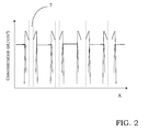
Figure 2 schematically shows the dopant concentration profiles of an embodiment of the structure ofFigure 1 ; -
Figures 3A-3D schematically show section views of the structure ofFigure 1 during different steps of the integration process according to the invention. - With reference to such figures, and in particular to
Figure 1, 1 globally and schematically indicates a structure for a high voltage device according to the invention. - It is suitable to note that figures showing schematic portions of the integrate structure are not drawn in scale, but are drawn in such a way to emphasise the important features of the invention.
- Moreover, the process steps as herein below described do not form a complete process flow for manufacturing high voltage devices. The present invention can be reduced into practice along with techniques for manufacturing high voltage devices as currently used into the field, and only those process steps which are needed for understanding the present invention are included.
- The
structure 1 for a high voltage device comprises asemiconductor substrate 2 covered by anepitaxial layer 3, having a first conductivity type, in particular N type. Advantageously according to an embodiment of the invention, a plurality ofcolumn structures 4 having a high aspect ratio, in particular less than 3/20, is realised in theepitaxial layer 3. - The
structure 1 for a high voltage device further comprises anactive surface area 5, wherein the active areas of the high voltage device are realised, as will be clarified in the following description. - According to an embodiment of the invention, each of the
column structures 4 comprises anexternal portion 6, in particular an epitaxial silicon layer being suitably doped, as well as a fillingportion 7, in particular a dielectric layer, such as an oxide, being deposited inside therespective column structure 4 for completely filling it. The epitaxial silicon layer of theexternal portion 6 is doped and has a second conductivity type, in particular the P type. - According to an embodiment of the invention, the charge which is epitaxially inserted in order to realise the
external portion 6 is such as to counterbalance the charge being in theepitaxial layer 3 outside thecolumn structures 4. Moreover, according to an embodiment of the invention, the epitaxial layer, which realises theexternal portion 6 is on the walls and on the bottom of thecorresponding column structure 4, which is realised, as will be clarified in the following description, starting from a trench being dug in theepitaxial layer 3, in particular a deep trench having a high aspect ratio, i.e. a low ratio between width and height, for instance less than 3/20. - In the
active surface area 5, a high voltage device is realised, in a conventional manner, of the type comprising at least anactive area 8. - According to an embodiment of the invention, the
column structures 4 haverespective fastening zones 12 with theactive areas 8, having a same periodicity thereof. - In particular, the
structure 1 for a high voltage device according to the invention comprisescolumn structures 4 in turn realised by a U-shaped zone of semiconductor material, i.e. theexternal portion 6 of the epitaxial silicon, being suitably doped with a dopand of an opposite type with respect to the one of the neighbouring semiconductor material, i.e. theepitaxial layer 3 outside thecolumn structures 4, this U-shapedexternal portion 6 being in turn filled by a dielectric layer to form the fillingportion 7. - It is suitable to note that, according to an embodiment of the invention, the charge quantity being in the epitaxial silicon layer of the U-shaped
external portion 6 of thecolumn structures 4 is such that a balance of the charge is obtained with respect to theepitaxial layer 3 outside thecolumn structures 4 themselves. - In the example of
Figure 1 , a MOS transistor of the Multi Drain type is realised. - Therefore, in the example as shown, the MOS transistor comprises a
drain epitaxial layer 3 being provided with a plurality ofcolumn structures 4 and anactive surface area 5 wherein a plurality ofbody wells 8 are realised, having the second conductivity type, in particular the P type, inside which a corresponding plurality ofsource wells 9, of the first conductivity type, in particular the N type, is realised. - The high voltage MOS device of the example of
Figure 1 is completed by realising a plurality ofgate structures 10, being realised between consecutive pairs ofcolumn structures 4, above a channel region, being defined in thedrain epitaxial layer 3 between thebody wells 8 and in contact with thesource wells 9. - The
structure 1 for a high voltage device further comprises a covering or cappinglayer 11, being realised above the whole high voltage device and in particular covering thegate structures 10. - Finally, the
structure 1 for a high voltage device could be provided, in a known manner, with surface contact structures of microtrench or conventional type. - Moreover, the
gate structures 10 could be of the planar type or of the trench gate type. - According to an embodiment of the invention, the
drain column structures 4, having a same periodicity than thebody wells 8, haverespective fastening zones 12 with thebody wells 8 themselves. In particular, each of thecolumn structures 4 comprises a pair offastening zones 12 with thebody wells 8 which bounds it at the upper side. - In a preferred embodiment of the
structure 1 for a high voltage device according to the invention, each of thecolumn structures 4 has a width Lc between 1,5 and 4um, preferably 2um and a height Hc between 10 and 70 um, preferably 30um, thus defining a maximum value of aspect ratio of the deep trench which constitutes thecolumn structures 4 equal to 3/20. - Moreover, according to a preferred embodiment of the invention, the epitaxial layer which realises the
external portion 6 has a dopant concentration between 1e15 and 1e17, preferably 1e16 at/cm3, while thedrain epitaxial layer 3 has a dopant concentration between 5e14 and 5e16, preferably 5e15. - In a further preferred embodiment, the
column structures 4 have a distance Dc between 2um and 8um, preferably 4um, and a distance Dcc between the symmetry axis of thecolumn structures 4 between 2.5um and 12um, preferably 6um. - In a preferred embodiment, the
structure 1 for a high voltage device according to the invention realises a 600V device. - By varying the height Hc of the
column structures 4, it is however possible to easily obtain high voltage devices from 300V up to 2000V. - The dopant concentration along the
column structures 4 of an embodiment of thestructure 1 for a high voltage device according to the invention is shown inFigure 2A , X being the longitudinal development axis of thestructure 1 itself, as also indicated inFigure 1 . In particular, it is worth noting that the charge epitaxially introduced into the epitaxial layer which realises the U-shapedexternal portion 6 of thecolumn structures 4 is such that it counterbalances the charge being in theepitaxial layer 3 outside thecolumn structures 4 themselves, the fillingportion 7 ofsuch column structures 4 being instead realised by an oxide. - According to this embodiment, the dopant in the epitaxial layer forming the U-shaped
external portion 6 of thecolumn structures 4 is not constant, but it advantageously has a peack in correspondence with the interface with theepitaxial layer 3 outside thecolumn structures 4 themselves. - According to this embodiment, the manufacturing process of the
structure 1 for a high voltage device turns out to be well controlled since it is able to guarantee the charge balance between the U-shapedexternal portion 6 of thecolumn structures 4 and theepitaxial layer 3 outside them (i.e. between the N zone and the P zone) without needing an extremely fine control of the thickness of the silicon epitaxial layer as grown in order to realise the U-shapedexternal portion 6. In particular, in the case under examination, changes into the thickness of theexternal portion 6 cause little changes on the total charge amount being contained into the silicon epitaxial layer of suchexternal portion 6 thus making easier the process industrialisation. - While in the embodiment as shown in
Figure 1 thecolumn structures 4 do not reach thesemiconductor substrate 2, it is obviously possible to take into account the case in which they reach it too. - Moreover, it is obviously possible to realise in the active surface area 5 a high voltage device different from a MOS transistor, such as for example a diode or an IGBT device.
- In essence, it is possible to consider the
structure 1 for a high voltage device according to the invention as comprising a first active area being realised by thecolumn structures 4 and a secondactive area 8 and having at least onefastening zone 12 which the firstactive area 4. - According to an embodiment of the invention, the second active area is "fastened" in correspondence with the
fastening zone 12 to a conductive portion of the first active area, in particular of the column structures. - In the case shown in
Figure 1 , making a MOS transistor of the Multi Drain type, the first active area is the drain area while the second one is the body area. It is obvious for a technical expert in the field that, in the case for instance of a diode, such first and second active areas would be the cathode and anode areas. - Also in the exemplary case of
Figure 1 , the second active area is "fastened" in correspondence with thefastening zone 12 to theexternal portion 6 of thecolumn structure 4, being a conductive portion of the first active area. - The present invention also relates to an integration process of a
structure 1 for a high voltage device of the above indicated type. - This integration process essentially comprises the steps of:
- realising a
semiconductor substrate 2 having a first conductivity type; - epitaxially growing on
such semiconductor substrate 2 anepitaxial layer 3 having the first conductivity type; and - realising in said
epitaxial layer 3 at least adeep trench 4 having a high aspect ratio in order to realise at least one column structure, as schematically shown inFigure 3A . - The process according to an embodiment of the invention further comprises the step of epitaxially growing within the
trench 4 of asilicon layer 6, being placed at least on the walls and on the bottom of thetrench 4 so as to realise an external portion of acolumn structure 4 being thus formed into theepitaxial layer 3. - According to an embodiment of the invention, the
epitaxial layer 6 having been grown to form such an external portion is doped with a dopant of a second type and in such a way that the dopant charge being epitaxially introduced counterbalances the charge of the dopant of the first type of theepitaxial layer 3 surrounding thetrench 4, as schematically shown inFigure 3B . - Said epitaxial growing step advantageously grows an
epitaxial layer 6 having a dopant concentration with a variable concentration profile having a maximum near an interface with theepitaxial layer 3. - Advantageously according to the invention, the steps of epitaxially growing the
drain epitaxial layer 3 and theepitaxial layer 6 of the external portion of the column structures are realised with a limited thermal budget and a maximum process temperature less than 1100°C. In this way, the process according to the invention turns out to be compatible also with big sized wafers (for instance of 8" or 12") and it is possible to minimize the transition zone between thecolumn structures 4 and the conduction zones, i.e. the portions of thedrain epitaxial layer 3 outside saidcolumn structures 4. - In other words, a process having a low thermal budget is used in order to keep almost unaltered the dopant distribution inside the
epitaxial layer 3 having been grown inside thetrench 4 which makes the column structures. - In particular, the epitaxial growing steps realising the
epitaxial layer 6 with a dopant concentration between 1e15 and 1e17, preferably 1e16 at/cm3, and adrain epitaxial layer 3 with a dopant concentration between 5e14 and 5e16, preferably 5e15. - Furthermore, the process comprises a filling step of the
trench 4 by means of a fillingdielectric layer 7, in particular an oxide, in order to realise a filling portion of thecolumn structure 4, as schematically shown inFigure 3C . - This filling step by means of the filling
dielectric layer 7 completely fills thetrench 4, guaranteeing the absence into the same, and thus into thecolumn structure 4 so realized, of voids. - The process then comprises a step of realising, in an
active surface area 5 of thestructure 1, a high voltage device comprising at least an active area. In particular, as in the example shown inFigure 1 , the high voltage device is a MOS transistor of the Multi Drain type comprising a drain area being realised by theepitaxial layer 3 and thecolumn structures 4 and comprisingsource wells 9 being realised intobody wells 8, these latter having been advantageously realised in contact with thecolumn structures 4 in correspondence withfastening zones 12, as well asgate structures 10 being realized over channel regions being defined into theepitaxial layer 3 between thebody wells 8 and in contact with thesource wells 9, as schematically shown inFigure 3D . - It is thus obtained an integration process having a lower number of steps that a conventional technology of integration of Multi Drain transistors and thus being easier to implement.
- Moreover, the charge balance being realised by the
epitaxial layer 6 of the external portion of thecolumn structures 4 with respect to theepitaxial layer 3 which surrounds them, allows to obtain a constant dopant profile in the conduction zone, the extension of the voltage class of the high voltage device so obtained being thus easier. - According to an embodiment of the invention, the use of an epitaxial growing step of the
layer 6 allows to eliminate every problem of implant angle tied to the high aspect ratio of thetrench 4, with a better doping control of theexternal portion 6 of thecolumn structures 4. - Obviously, a technician of the field, aiming at meeting incidental and specific needs, will bring several modifications and alternatives to the above described structure and process, all within the scope of protection of the invention as defined by the following claims. In particular, it is possible, by using a drain layer of the P type and column structures of the N type, to obtain a structure for a high voltage device of a dual type.
Claims (17)
- Structure (1) for a high voltage device of the type which comprises at least a semiconductor substrate (2) being covered by an epitaxial layer (3) of a first type of conductivity, wherein a plurality of column structures (4) are realised, which column structures comprise high aspect ratio deep trenches, said epitaxial layer (3) being in turn covered by an active surface area (5) wherein said high voltage device is realised, characterized in that each of the column structures (4) comprises at least an external portion (6) being in turn realised by a silicon epitaxial layer of a second type of conductivity, opposed than said first type of conductivity and having a dopant charge which counterbalances the dopant charge being in said epitaxial layer (3) outside said column structures (4), as well as a dielectric filling portion (7) which is realised inside said external portion (6) in order to completely fill said deep trench, said external portion (6) having a dopant concentration with a variable concentration profile having a maximum near an interface with said epitaxial layer (3).
- Structure (1) for a high voltage device according to claim 1, characterized in that said epitaxial layer of said external portion (6) is U-shaped and extends both on the wall and on the bottom of a corresponding column structure (4).
- Structure (1) for a high voltage device according to claim 1, characterized in that said external portion (6) has a dopant concentration between 1e15 and 1e17, preferably 1e16 at/cm3 and said epitaxial layer (3) has a dopant concentration between 5e14 and 5e16, preferably 5e15.
- Structure (1) for a high voltage device according to claim 1, characterized in that said column structures (4) have a ratio between width and height less than 3/20.
- Structure (1) for a high voltage device according to claim 1, characterized in that said column structures (4) realise a first active area of said high voltage device and in that said high voltage device comprises at least a second active area (8) which is realised in said active surface area (5) and has at least one fastening zone (12) with said first active area.
- Structure (1) for a high voltage device according to claim 5, characterized in that said first active area is fastened in correspondence with said fastening zone (12) to a conduction portion (6) of said first active area.
- Structure (1) for a high voltage device according to claim 4, characterized in that said column structures (4) have a same periodicity with respect to said second active areas (8).
- Structure (1) for a high voltage device according to claim 1, characterized in that said column structures (4) extend down to said semiconductor substrate (2).
- Structure (1) for a high voltage device according to claim 1, characterized in that said column structures (4) extend down to a prefixed distance from said semiconductor substrate (2).
- Structure (1) for a high voltage device according to any of the preceding claims, characterized in that said high voltage device is a MOS transistor of the Multi Drain type and in that said first active area is a drain area comprising said epitaxial layer (3) and said column structures (4) and in that said second active area is a body area (8).
- Structure (1) for a high voltage device according to claim 10, characterized in that said high voltage device comprises, in said active surface area (5), a plurality of body wells (8) of said second type of conductivity, inside which corresponding plurality of source wells (9) of said first type of conductivity are realised, as well as a plurality of gate structures (10), being realised between consecutive pairs of column structures (4), above a channel region being define in said epitaxial layer (3) between said body wells (8) and in contact with said source wells (9).
- Structure (1) for a high voltage device according to claim 11, characterized in that said gate structures (10) are chosen between planar type and trench gate type structures.
- Integration process of a structure (1) for a high voltage device of the type which comprises the steps of:- realising a semiconductor substrate (2) having a first conductivity type;- epitaxially growing on said semiconductor substrate (2) an epitaxial layer (3) having said first conductivity type; and- realising in said epitaxial layer (3) at least one deep trench (4) having a high aspect ratio in order to realise at least one column structure (4) in said epitaxial layer (3);characterized in that it further comprises:- an epitaxial growing step within said trench (4) of a silicon layer (6) being doped and having a second conductivity type, opposed than said first conductivity type and having a dopant charge which counterbalances a dopant charge being in said epitaxial layer (3) outside said column structures (4) and- a filling step of said trench (4) by means of a filling dielectric layer (7) in order to realise a filling portion (7) of said at least one column structure (4)said epitaxial growing step growing a silicon layer (6) having a dopant concentration with a variable concentration profile having a maximum near an interface with said epitaxial layer (3).
- Integration process according to claim 13, characterized in that said epitaxial growing step within said trench (4) grows said silicon layer (6) at least on the walls and on the bottom of said trench (4) thus realising an U-shaped external portion (6) of said at least one column structure (4).
- Integration process according to claim 13, characterized in that said epitaxial growing steps of said epitaxial layer (3) on said semiconductor substrate (2) and of said epitaxial layer (6) within said trench (4) are realised with a limited thermal budget and with a process maximum temperature less than 1100°C.
- Integration process according to claim 15, characterized in that said epitaxial growing steps realise said epitaxial layer (6) within said trench (4) with a dopant concentration comprised between 1e15 and 1e17, preferably 1e16 at/cm3, and said epitaxial layer (3) on said semiconductor substrate (2) with a dopant concentration comprised between 5e14 and 5e16, preferably 5e15.
- Integration process according to claim 13, characterized in that said column structures (4) realise a first active area of said high voltage device and in that if further comprises a step of realising, in an active surface area (5) of said structure (1), at least one second active area (8) which has at least one fastening zone (12) with said first active area.
Applications Claiming Priority (1)
| Application Number | Priority Date | Filing Date | Title |
|---|---|---|---|
| ITMI20091522 | 2009-09-01 |
Publications (2)
| Publication Number | Publication Date |
|---|---|
| EP2290697A1 true EP2290697A1 (en) | 2011-03-02 |
| EP2290697B1 EP2290697B1 (en) | 2016-07-06 |
Family
ID=42134235
Family Applications (1)
| Application Number | Title | Priority Date | Filing Date |
|---|---|---|---|
| EP10174803.6A Active EP2290697B1 (en) | 2009-09-01 | 2010-09-01 | Method of making high-voltage semiconductor device with column structures |
Country Status (2)
| Country | Link |
|---|---|
| US (2) | US20110049638A1 (en) |
| EP (1) | EP2290697B1 (en) |
Cited By (4)
| Publication number | Priority date | Publication date | Assignee | Title |
|---|---|---|---|---|
| WO2012163048A1 (en) * | 2011-06-03 | 2012-12-06 | Tsinghua University | Semiconductor structure and method for forming the same |
| CN105789270A (en) * | 2016-04-21 | 2016-07-20 | 西安电子科技大学 | VDMOS device with variable dielectric side |
| NL2018612A (en) * | 2016-03-31 | 2017-10-05 | Shindengen Electric Mfg | Semiconductor device and method of manufacturing semiconductor device |
| CN108389892A (en) * | 2018-02-02 | 2018-08-10 | 电子科技大学 | A kind of lateral resistance to pressure area of the shallow/deep groove type with longitudinal varying doping dosage |
Families Citing this family (4)
| Publication number | Priority date | Publication date | Assignee | Title |
|---|---|---|---|---|
| US9318554B2 (en) * | 2013-03-13 | 2016-04-19 | Michael Wayne Shore | Gate pad and gate feed breakdown voltage enhancement |
| US9558986B2 (en) * | 2013-09-18 | 2017-01-31 | Taiwan Semiconductor Manufacturing Company Ltd. | Semiconductor structure and manufacturing method thereof |
| CN107482060A (en) * | 2016-06-08 | 2017-12-15 | 深圳尚阳通科技有限公司 | Superjunction device and method of manufacturing the same |
| US10217761B1 (en) | 2017-11-22 | 2019-02-26 | Macronix International Co., Ltd. | Semiconductor structure and manufacturing method thereof |
Citations (9)
| Publication number | Priority date | Publication date | Assignee | Title |
|---|---|---|---|---|
| US6228719B1 (en) | 1995-11-06 | 2001-05-08 | Stmicroelectronics S.R.L. | MOS technology power device with low output resistance and low capacitance, and related manufacturing process |
| US6300171B1 (en) | 1998-12-09 | 2001-10-09 | Stmicroelectronics S.R.L. | Method of manufacturing an integrated edge structure for high voltage semiconductor devices, and related integrated edge structure |
| US20010055861A1 (en) | 2000-04-04 | 2001-12-27 | Davide Patti | Process for manufacturing deep well junction structures |
| US6404010B2 (en) | 2000-05-19 | 2002-06-11 | Stmicroelectronics S.R.L. | MOS technology power device |
| US6410958B1 (en) | 2000-11-27 | 2002-06-25 | Kabushiki Kaisha Toshiba | Power MOSFET having laterally three-layered structure formed among element isolation regions |
| EP1267415A2 (en) * | 2001-06-11 | 2002-12-18 | Kabushiki Kaisha Toshiba | Power semiconductor device having resurf layer |
| US6586798B1 (en) | 1998-12-09 | 2003-07-01 | Stmicroelectronics S.R.L. | High voltage MOS-gated power device |
| US20080038850A1 (en) * | 2006-08-11 | 2008-02-14 | Denso Corporation | Method for manufacturing semiconductor device |
| US7498619B2 (en) | 2005-02-25 | 2009-03-03 | Stmicroelectronics S.R.L. | Power electronic device of multi-drain type integrated on a semiconductor substrate and relative manufacturing process |
Family Cites Families (9)
| Publication number | Priority date | Publication date | Assignee | Title |
|---|---|---|---|---|
| JP3291957B2 (en) * | 1995-02-17 | 2002-06-17 | 富士電機株式会社 | Vertical trench MISFET and method of manufacturing the same |
| US6713813B2 (en) * | 2001-01-30 | 2004-03-30 | Fairchild Semiconductor Corporation | Field effect transistor having a lateral depletion structure |
| US6803626B2 (en) * | 2002-07-18 | 2004-10-12 | Fairchild Semiconductor Corporation | Vertical charge control semiconductor device |
| US7638841B2 (en) * | 2003-05-20 | 2009-12-29 | Fairchild Semiconductor Corporation | Power semiconductor devices and methods of manufacture |
| AT504290A2 (en) * | 2005-06-10 | 2008-04-15 | Fairchild Semiconductor | FIELD EFFECT TRANSISTOR WITH LOAD BALANCE |
| EP1742259A1 (en) | 2005-07-08 | 2007-01-10 | STMicroelectronics S.r.l. | Semiconductor power device with multiple drain structure and corresponding manufacturing process |
| EP1742258A1 (en) | 2005-07-08 | 2007-01-10 | STMicroelectronics S.r.l. | Semiconductor power device with multiple drain and corresponding manufacturing process |
| US8304311B2 (en) | 2006-04-11 | 2012-11-06 | Stmicroelectronics S.R.L. | Process for manufacturing a semiconductor power device comprising charge-balance column structures and respective device |
| US7851897B1 (en) * | 2008-06-16 | 2010-12-14 | Maxim Integrated Products, Inc. | IC package structures for high power dissipation and low RDSon |
-
2010
- 2010-08-25 US US12/868,023 patent/US20110049638A1/en not_active Abandoned
- 2010-09-01 EP EP10174803.6A patent/EP2290697B1/en active Active
-
2015
- 2015-08-12 US US14/824,813 patent/US9627472B2/en active Active
Patent Citations (9)
| Publication number | Priority date | Publication date | Assignee | Title |
|---|---|---|---|---|
| US6228719B1 (en) | 1995-11-06 | 2001-05-08 | Stmicroelectronics S.R.L. | MOS technology power device with low output resistance and low capacitance, and related manufacturing process |
| US6300171B1 (en) | 1998-12-09 | 2001-10-09 | Stmicroelectronics S.R.L. | Method of manufacturing an integrated edge structure for high voltage semiconductor devices, and related integrated edge structure |
| US6586798B1 (en) | 1998-12-09 | 2003-07-01 | Stmicroelectronics S.R.L. | High voltage MOS-gated power device |
| US20010055861A1 (en) | 2000-04-04 | 2001-12-27 | Davide Patti | Process for manufacturing deep well junction structures |
| US6404010B2 (en) | 2000-05-19 | 2002-06-11 | Stmicroelectronics S.R.L. | MOS technology power device |
| US6410958B1 (en) | 2000-11-27 | 2002-06-25 | Kabushiki Kaisha Toshiba | Power MOSFET having laterally three-layered structure formed among element isolation regions |
| EP1267415A2 (en) * | 2001-06-11 | 2002-12-18 | Kabushiki Kaisha Toshiba | Power semiconductor device having resurf layer |
| US7498619B2 (en) | 2005-02-25 | 2009-03-03 | Stmicroelectronics S.R.L. | Power electronic device of multi-drain type integrated on a semiconductor substrate and relative manufacturing process |
| US20080038850A1 (en) * | 2006-08-11 | 2008-02-14 | Denso Corporation | Method for manufacturing semiconductor device |
Non-Patent Citations (3)
| Title |
|---|
| LIANG ET AL.: "Oxide-Bypassed VDMOS (OBVDMOS): An Alternative to Superjunction High Voltage MOS Power Devices", IEEE ELECTRON DEVICES LETTERS, vol. 22, no. 8, August 2001 (2001-08-01) |
| NITTA ET AL.: "12th International symposium on power semiconductor devices & Ics, Toulouse", 22 May 2000, MITSUBISHI ELECTRIC CO., article "Experimental Results and Simulation Analysis of 250V Super Trench Power MOSFET (STM)" |
| RUB ET AL.: "A Novel Trench Concept for the Fabrication of Compensation Devices", ISPSD, 14 April 2003 (2003-04-14) |
Cited By (6)
| Publication number | Priority date | Publication date | Assignee | Title |
|---|---|---|---|---|
| WO2012163048A1 (en) * | 2011-06-03 | 2012-12-06 | Tsinghua University | Semiconductor structure and method for forming the same |
| NL2018612A (en) * | 2016-03-31 | 2017-10-05 | Shindengen Electric Mfg | Semiconductor device and method of manufacturing semiconductor device |
| US10411141B2 (en) | 2016-03-31 | 2019-09-10 | Shindengen Electric Manufacturing Co., Ltd. | Semiconductor device and method of manufacturing semiconductor device |
| CN105789270A (en) * | 2016-04-21 | 2016-07-20 | 西安电子科技大学 | VDMOS device with variable dielectric side |
| CN108389892A (en) * | 2018-02-02 | 2018-08-10 | 电子科技大学 | A kind of lateral resistance to pressure area of the shallow/deep groove type with longitudinal varying doping dosage |
| CN108389892B (en) * | 2018-02-02 | 2020-08-11 | 电子科技大学 | A deep trench lateral withstand voltage region with longitudinally variable doping dose |
Also Published As
| Publication number | Publication date |
|---|---|
| US9627472B2 (en) | 2017-04-18 |
| US20110049638A1 (en) | 2011-03-03 |
| US20150349052A1 (en) | 2015-12-03 |
| EP2290697B1 (en) | 2016-07-06 |
Similar Documents
| Publication | Publication Date | Title |
|---|---|---|
| US9627472B2 (en) | Semiconductor structure with varying doping profile and related ICS and devices | |
| EP1803159B1 (en) | Mos-gated transistor with reduced miller capacitance | |
| TWI542020B (en) | Charge balance field effect transistor | |
| USRE46799E1 (en) | Semiconductor device with alternating conductivity type layers having different vertical impurity concentration profiles | |
| US8900949B2 (en) | Staggered column superjunction | |
| DE112004003046B4 (en) | Power semiconductor devices | |
| CN100342505C (en) | Method for fabricating a high voltage power MOSFET having a voltage sustaining region that includes doped columns formed by rapid diffusion | |
| JP5298432B2 (en) | Semiconductor device and manufacturing method thereof | |
| US7084455B2 (en) | Power semiconductor device having a voltage sustaining region that includes terraced trench with continuous doped columns formed in an epitaxial layer | |
| US7091552B2 (en) | High voltage power MOSFET having a voltage sustaining region that includes doped columns formed by trench etching and ion implantation | |
| CN102148163B (en) | Methods for manufacturing superjunction structure and superjunction semiconductor device | |
| US20120043602A1 (en) | Power MOSFET and Its Edge Termination | |
| US20100314682A1 (en) | Configurations and methods for manufacturing devices with trench-oxide-nano-tube super-junctions | |
| WO2010120704A2 (en) | Power semiconductor devices, methods, and structures with embedded dielectric layers containing permanent charges | |
| US20040150039A1 (en) | Trench MOSFET superjunction structure and method to manufacture | |
| JP2011512677A (en) | Semiconductor device structure and related processes | |
| JP2013503492A (en) | Manufacture of super junction trench power MOSFET devices | |
| CN101189710A (en) | Superjunction device with oxide lined trench and method of fabricating superjunction device with oxide lined trench | |
| US10014365B2 (en) | Power semiconductor devices, methods, and structures with embedded dielectric layers containing permanent charges | |
| CN110010693A (en) | A structure of a high-voltage deep trench type superjunction MOSFET and a manufacturing method thereof | |
| CN113517334A (en) | A kind of power MOSFET device with high-K dielectric trench and preparation method thereof | |
| JP5609950B2 (en) | Semiconductor device and manufacturing method thereof | |
| HK1112111B (en) | Mos-gated transistor with reduced miller capacitance |
Legal Events
| Date | Code | Title | Description |
|---|---|---|---|
| PUAI | Public reference made under article 153(3) epc to a published international application that has entered the european phase |
Free format text: ORIGINAL CODE: 0009012 |
|
| AK | Designated contracting states |
Kind code of ref document: A1 Designated state(s): AL AT BE BG CH CY CZ DE DK EE ES FI FR GB GR HR HU IE IS IT LI LT LU LV MC MK MT NL NO PL PT RO SE SI SK SM TR |
|
| AX | Request for extension of the european patent |
Extension state: BA ME RS |
|
| RAP1 | Party data changed (applicant data changed or rights of an application transferred) |
Owner name: STMICROELECTRONICS S.R.L. |
|
| 17P | Request for examination filed |
Effective date: 20110902 |
|
| RAP1 | Party data changed (applicant data changed or rights of an application transferred) |
Owner name: STMICROELECTRONICS SRL |
|
| 17Q | First examination report despatched |
Effective date: 20130916 |
|
| GRAP | Despatch of communication of intention to grant a patent |
Free format text: ORIGINAL CODE: EPIDOSNIGR1 |
|
| INTG | Intention to grant announced |
Effective date: 20160126 |
|
| GRAS | Grant fee paid |
Free format text: ORIGINAL CODE: EPIDOSNIGR3 |
|
| GRAA | (expected) grant |
Free format text: ORIGINAL CODE: 0009210 |
|
| AK | Designated contracting states |
Kind code of ref document: B1 Designated state(s): AL AT BE BG CH CY CZ DE DK EE ES FI FR GB GR HR HU IE IS IT LI LT LU LV MC MK MT NL NO PL PT RO SE SI SK SM TR |
|
| REG | Reference to a national code |
Ref country code: GB Ref legal event code: FG4D |
|
| REG | Reference to a national code |
Ref country code: AT Ref legal event code: REF Ref document number: 811251 Country of ref document: AT Kind code of ref document: T Effective date: 20160715 Ref country code: CH Ref legal event code: EP |
|
| REG | Reference to a national code |
Ref country code: IE Ref legal event code: FG4D |
|
| REG | Reference to a national code |
Ref country code: DE Ref legal event code: R096 Ref document number: 602010034436 Country of ref document: DE |
|
| REG | Reference to a national code |
Ref country code: FR Ref legal event code: PLFP Year of fee payment: 7 |
|
| REG | Reference to a national code |
Ref country code: NL Ref legal event code: MP Effective date: 20160706 |
|
| REG | Reference to a national code |
Ref country code: LT Ref legal event code: MG4D |
|
| REG | Reference to a national code |
Ref country code: AT Ref legal event code: MK05 Ref document number: 811251 Country of ref document: AT Kind code of ref document: T Effective date: 20160706 |
|
| PG25 | Lapsed in a contracting state [announced via postgrant information from national office to epo] |
Ref country code: NL Free format text: LAPSE BECAUSE OF FAILURE TO SUBMIT A TRANSLATION OF THE DESCRIPTION OR TO PAY THE FEE WITHIN THE PRESCRIBED TIME-LIMIT Effective date: 20160706 Ref country code: HR Free format text: LAPSE BECAUSE OF FAILURE TO SUBMIT A TRANSLATION OF THE DESCRIPTION OR TO PAY THE FEE WITHIN THE PRESCRIBED TIME-LIMIT Effective date: 20160706 Ref country code: IS Free format text: LAPSE BECAUSE OF FAILURE TO SUBMIT A TRANSLATION OF THE DESCRIPTION OR TO PAY THE FEE WITHIN THE PRESCRIBED TIME-LIMIT Effective date: 20161106 Ref country code: NO Free format text: LAPSE BECAUSE OF FAILURE TO SUBMIT A TRANSLATION OF THE DESCRIPTION OR TO PAY THE FEE WITHIN THE PRESCRIBED TIME-LIMIT Effective date: 20161006 Ref country code: FI Free format text: LAPSE BECAUSE OF FAILURE TO SUBMIT A TRANSLATION OF THE DESCRIPTION OR TO PAY THE FEE WITHIN THE PRESCRIBED TIME-LIMIT Effective date: 20160706 Ref country code: IT Free format text: LAPSE BECAUSE OF FAILURE TO SUBMIT A TRANSLATION OF THE DESCRIPTION OR TO PAY THE FEE WITHIN THE PRESCRIBED TIME-LIMIT Effective date: 20160706 Ref country code: LT Free format text: LAPSE BECAUSE OF FAILURE TO SUBMIT A TRANSLATION OF THE DESCRIPTION OR TO PAY THE FEE WITHIN THE PRESCRIBED TIME-LIMIT Effective date: 20160706 |
|
| PG25 | Lapsed in a contracting state [announced via postgrant information from national office to epo] |
Ref country code: GR Free format text: LAPSE BECAUSE OF FAILURE TO SUBMIT A TRANSLATION OF THE DESCRIPTION OR TO PAY THE FEE WITHIN THE PRESCRIBED TIME-LIMIT Effective date: 20161007 Ref country code: ES Free format text: LAPSE BECAUSE OF FAILURE TO SUBMIT A TRANSLATION OF THE DESCRIPTION OR TO PAY THE FEE WITHIN THE PRESCRIBED TIME-LIMIT Effective date: 20160706 Ref country code: BE Free format text: LAPSE BECAUSE OF NON-PAYMENT OF DUE FEES Effective date: 20160706 Ref country code: PT Free format text: LAPSE BECAUSE OF FAILURE TO SUBMIT A TRANSLATION OF THE DESCRIPTION OR TO PAY THE FEE WITHIN THE PRESCRIBED TIME-LIMIT Effective date: 20161107 Ref country code: LV Free format text: LAPSE BECAUSE OF FAILURE TO SUBMIT A TRANSLATION OF THE DESCRIPTION OR TO PAY THE FEE WITHIN THE PRESCRIBED TIME-LIMIT Effective date: 20160706 Ref country code: PL Free format text: LAPSE BECAUSE OF FAILURE TO SUBMIT A TRANSLATION OF THE DESCRIPTION OR TO PAY THE FEE WITHIN THE PRESCRIBED TIME-LIMIT Effective date: 20160706 Ref country code: AT Free format text: LAPSE BECAUSE OF FAILURE TO SUBMIT A TRANSLATION OF THE DESCRIPTION OR TO PAY THE FEE WITHIN THE PRESCRIBED TIME-LIMIT Effective date: 20160706 Ref country code: SE Free format text: LAPSE BECAUSE OF FAILURE TO SUBMIT A TRANSLATION OF THE DESCRIPTION OR TO PAY THE FEE WITHIN THE PRESCRIBED TIME-LIMIT Effective date: 20160706 |
|
| REG | Reference to a national code |
Ref country code: DE Ref legal event code: R097 Ref document number: 602010034436 Country of ref document: DE |
|
| PG25 | Lapsed in a contracting state [announced via postgrant information from national office to epo] |
Ref country code: MC Free format text: LAPSE BECAUSE OF FAILURE TO SUBMIT A TRANSLATION OF THE DESCRIPTION OR TO PAY THE FEE WITHIN THE PRESCRIBED TIME-LIMIT Effective date: 20160706 Ref country code: RO Free format text: LAPSE BECAUSE OF FAILURE TO SUBMIT A TRANSLATION OF THE DESCRIPTION OR TO PAY THE FEE WITHIN THE PRESCRIBED TIME-LIMIT Effective date: 20160706 Ref country code: EE Free format text: LAPSE BECAUSE OF FAILURE TO SUBMIT A TRANSLATION OF THE DESCRIPTION OR TO PAY THE FEE WITHIN THE PRESCRIBED TIME-LIMIT Effective date: 20160706 |
|
| REG | Reference to a national code |
Ref country code: CH Ref legal event code: PL |
|
| PLBE | No opposition filed within time limit |
Free format text: ORIGINAL CODE: 0009261 |
|
| STAA | Information on the status of an ep patent application or granted ep patent |
Free format text: STATUS: NO OPPOSITION FILED WITHIN TIME LIMIT |
|
| PG25 | Lapsed in a contracting state [announced via postgrant information from national office to epo] |
Ref country code: DK Free format text: LAPSE BECAUSE OF FAILURE TO SUBMIT A TRANSLATION OF THE DESCRIPTION OR TO PAY THE FEE WITHIN THE PRESCRIBED TIME-LIMIT Effective date: 20160706 Ref country code: BG Free format text: LAPSE BECAUSE OF FAILURE TO SUBMIT A TRANSLATION OF THE DESCRIPTION OR TO PAY THE FEE WITHIN THE PRESCRIBED TIME-LIMIT Effective date: 20161006 Ref country code: SM Free format text: LAPSE BECAUSE OF FAILURE TO SUBMIT A TRANSLATION OF THE DESCRIPTION OR TO PAY THE FEE WITHIN THE PRESCRIBED TIME-LIMIT Effective date: 20160706 Ref country code: SK Free format text: LAPSE BECAUSE OF FAILURE TO SUBMIT A TRANSLATION OF THE DESCRIPTION OR TO PAY THE FEE WITHIN THE PRESCRIBED TIME-LIMIT Effective date: 20160706 Ref country code: CZ Free format text: LAPSE BECAUSE OF FAILURE TO SUBMIT A TRANSLATION OF THE DESCRIPTION OR TO PAY THE FEE WITHIN THE PRESCRIBED TIME-LIMIT Effective date: 20160706 |
|
| 26N | No opposition filed |
Effective date: 20170407 |
|
| GBPC | Gb: european patent ceased through non-payment of renewal fee |
Effective date: 20161006 |
|
| REG | Reference to a national code |
Ref country code: IE Ref legal event code: MM4A |
|
| REG | Reference to a national code |
Ref country code: DE Ref legal event code: R082 Ref document number: 602010034436 Country of ref document: DE Representative=s name: SCHMITT-NILSON SCHRAUD WAIBEL WOHLFROM PATENTA, DE |
|
| PG25 | Lapsed in a contracting state [announced via postgrant information from national office to epo] |
Ref country code: GB Free format text: LAPSE BECAUSE OF NON-PAYMENT OF DUE FEES Effective date: 20161006 Ref country code: CH Free format text: LAPSE BECAUSE OF NON-PAYMENT OF DUE FEES Effective date: 20160930 Ref country code: LI Free format text: LAPSE BECAUSE OF NON-PAYMENT OF DUE FEES Effective date: 20160930 Ref country code: IE Free format text: LAPSE BECAUSE OF NON-PAYMENT OF DUE FEES Effective date: 20160901 |
|
| REG | Reference to a national code |
Ref country code: FR Ref legal event code: PLFP Year of fee payment: 8 |
|
| PG25 | Lapsed in a contracting state [announced via postgrant information from national office to epo] |
Ref country code: LU Free format text: LAPSE BECAUSE OF NON-PAYMENT OF DUE FEES Effective date: 20160901 Ref country code: SI Free format text: LAPSE BECAUSE OF FAILURE TO SUBMIT A TRANSLATION OF THE DESCRIPTION OR TO PAY THE FEE WITHIN THE PRESCRIBED TIME-LIMIT Effective date: 20160706 |
|
| PG25 | Lapsed in a contracting state [announced via postgrant information from national office to epo] |
Ref country code: CY Free format text: LAPSE BECAUSE OF FAILURE TO SUBMIT A TRANSLATION OF THE DESCRIPTION OR TO PAY THE FEE WITHIN THE PRESCRIBED TIME-LIMIT Effective date: 20160706 Ref country code: HU Free format text: LAPSE BECAUSE OF FAILURE TO SUBMIT A TRANSLATION OF THE DESCRIPTION OR TO PAY THE FEE WITHIN THE PRESCRIBED TIME-LIMIT; INVALID AB INITIO Effective date: 20100901 |
|
| PG25 | Lapsed in a contracting state [announced via postgrant information from national office to epo] |
Ref country code: MT Free format text: LAPSE BECAUSE OF NON-PAYMENT OF DUE FEES Effective date: 20160930 Ref country code: MK Free format text: LAPSE BECAUSE OF FAILURE TO SUBMIT A TRANSLATION OF THE DESCRIPTION OR TO PAY THE FEE WITHIN THE PRESCRIBED TIME-LIMIT Effective date: 20160706 Ref country code: TR Free format text: LAPSE BECAUSE OF FAILURE TO SUBMIT A TRANSLATION OF THE DESCRIPTION OR TO PAY THE FEE WITHIN THE PRESCRIBED TIME-LIMIT Effective date: 20160706 |
|
| REG | Reference to a national code |
Ref country code: FR Ref legal event code: PLFP Year of fee payment: 9 |
|
| PG25 | Lapsed in a contracting state [announced via postgrant information from national office to epo] |
Ref country code: AL Free format text: LAPSE BECAUSE OF FAILURE TO SUBMIT A TRANSLATION OF THE DESCRIPTION OR TO PAY THE FEE WITHIN THE PRESCRIBED TIME-LIMIT Effective date: 20160706 |
|
| REG | Reference to a national code |
Ref country code: DE Ref legal event code: R079 Ref document number: 602010034436 Country of ref document: DE Free format text: PREVIOUS MAIN CLASS: H01L0029780000 Ipc: H10D0030600000 |
|
| PGFP | Annual fee paid to national office [announced via postgrant information from national office to epo] |
Ref country code: DE Payment date: 20250820 Year of fee payment: 16 |
|
| PGFP | Annual fee paid to national office [announced via postgrant information from national office to epo] |
Ref country code: FR Payment date: 20250820 Year of fee payment: 16 |