EP2287930A1 - Light emitting diode including barrier layers and manufacturing method therefore - Google Patents
Light emitting diode including barrier layers and manufacturing method therefore Download PDFInfo
- Publication number
- EP2287930A1 EP2287930A1 EP10185865A EP10185865A EP2287930A1 EP 2287930 A1 EP2287930 A1 EP 2287930A1 EP 10185865 A EP10185865 A EP 10185865A EP 10185865 A EP10185865 A EP 10185865A EP 2287930 A1 EP2287930 A1 EP 2287930A1
- Authority
- EP
- European Patent Office
- Prior art keywords
- sublayers
- layer
- light emitting
- reflector
- emitting device
- Prior art date
- Legal status (The legal status is an assumption and is not a legal conclusion. Google has not performed a legal analysis and makes no representation as to the accuracy of the status listed.)
- Granted
Links
- 238000004519 manufacturing process Methods 0.000 title claims description 10
- 230000004888 barrier function Effects 0.000 title abstract description 100
- 239000000758 substrate Substances 0.000 claims abstract description 64
- 239000004065 semiconductor Substances 0.000 claims abstract description 10
- 229910052751 metal Inorganic materials 0.000 claims description 53
- 239000002184 metal Substances 0.000 claims description 53
- PXHVJJICTQNCMI-UHFFFAOYSA-N Nickel Chemical compound [Ni] PXHVJJICTQNCMI-UHFFFAOYSA-N 0.000 claims description 51
- BASFCYQUMIYNBI-UHFFFAOYSA-N platinum Chemical compound [Pt] BASFCYQUMIYNBI-UHFFFAOYSA-N 0.000 claims description 30
- 238000000034 method Methods 0.000 claims description 28
- 239000010931 gold Substances 0.000 claims description 23
- 229910052759 nickel Inorganic materials 0.000 claims description 21
- 239000010936 titanium Substances 0.000 claims description 21
- 229910052719 titanium Inorganic materials 0.000 claims description 19
- 238000013508 migration Methods 0.000 claims description 17
- 230000005012 migration Effects 0.000 claims description 17
- 229910052737 gold Inorganic materials 0.000 claims description 16
- RTAQQCXQSZGOHL-UHFFFAOYSA-N Titanium Chemical compound [Ti] RTAQQCXQSZGOHL-UHFFFAOYSA-N 0.000 claims description 15
- 229910052697 platinum Inorganic materials 0.000 claims description 15
- 229910052709 silver Inorganic materials 0.000 claims description 13
- 239000004332 silver Substances 0.000 claims description 11
- JMASRVWKEDWRBT-UHFFFAOYSA-N Gallium nitride Chemical compound [Ga]#N JMASRVWKEDWRBT-UHFFFAOYSA-N 0.000 claims description 9
- 229910002601 GaN Inorganic materials 0.000 claims description 8
- 239000011449 brick Substances 0.000 claims description 6
- KDLHZDBZIXYQEI-UHFFFAOYSA-N Palladium Chemical compound [Pd] KDLHZDBZIXYQEI-UHFFFAOYSA-N 0.000 claims description 5
- 238000005336 cracking Methods 0.000 claims description 5
- 229910000480 nickel oxide Inorganic materials 0.000 claims description 4
- GNRSAWUEBMWBQH-UHFFFAOYSA-N oxonickel Chemical compound [Ni]=O GNRSAWUEBMWBQH-UHFFFAOYSA-N 0.000 claims description 4
- 230000001902 propagating effect Effects 0.000 claims description 4
- MAKDTFFYCIMFQP-UHFFFAOYSA-N titanium tungsten Chemical compound [Ti].[W] MAKDTFFYCIMFQP-UHFFFAOYSA-N 0.000 claims description 4
- 229910052763 palladium Inorganic materials 0.000 claims description 3
- 229910052782 aluminium Inorganic materials 0.000 claims description 2
- XAGFODPZIPBFFR-UHFFFAOYSA-N aluminium Chemical compound [Al] XAGFODPZIPBFFR-UHFFFAOYSA-N 0.000 claims 1
- 239000010410 layer Substances 0.000 description 285
- 229910000679 solder Inorganic materials 0.000 description 41
- 238000002161 passivation Methods 0.000 description 40
- HBMJWWWQQXIZIP-UHFFFAOYSA-N silicon carbide Chemical compound [Si+]#[C-] HBMJWWWQQXIZIP-UHFFFAOYSA-N 0.000 description 25
- 229910010271 silicon carbide Inorganic materials 0.000 description 23
- WFKWXMTUELFFGS-UHFFFAOYSA-N tungsten Chemical compound [W] WFKWXMTUELFFGS-UHFFFAOYSA-N 0.000 description 20
- 229910052721 tungsten Inorganic materials 0.000 description 20
- 239000010937 tungsten Substances 0.000 description 16
- 239000000463 material Substances 0.000 description 13
- 229910052718 tin Inorganic materials 0.000 description 13
- ATJFFYVFTNAWJD-UHFFFAOYSA-N Tin Chemical compound [Sn] ATJFFYVFTNAWJD-UHFFFAOYSA-N 0.000 description 10
- 230000015556 catabolic process Effects 0.000 description 10
- 238000006731 degradation reaction Methods 0.000 description 10
- 238000012360 testing method Methods 0.000 description 9
- VYPSYNLAJGMNEJ-UHFFFAOYSA-N Silicium dioxide Chemical compound O=[Si]=O VYPSYNLAJGMNEJ-UHFFFAOYSA-N 0.000 description 8
- BQCADISMDOOEFD-UHFFFAOYSA-N Silver Chemical compound [Ag] BQCADISMDOOEFD-UHFFFAOYSA-N 0.000 description 8
- 238000009736 wetting Methods 0.000 description 8
- 239000004593 Epoxy Substances 0.000 description 7
- 229910052594 sapphire Inorganic materials 0.000 description 7
- 239000010980 sapphire Substances 0.000 description 7
- 230000015572 biosynthetic process Effects 0.000 description 6
- PCHJSUWPFVWCPO-UHFFFAOYSA-N gold Chemical compound [Au] PCHJSUWPFVWCPO-UHFFFAOYSA-N 0.000 description 6
- 238000012545 processing Methods 0.000 description 6
- 238000000151 deposition Methods 0.000 description 5
- 150000002739 metals Chemical class 0.000 description 5
- 230000008021 deposition Effects 0.000 description 4
- 230000000694 effects Effects 0.000 description 4
- 230000005496 eutectics Effects 0.000 description 4
- 230000003287 optical effect Effects 0.000 description 4
- 238000004806 packaging method and process Methods 0.000 description 4
- 239000002243 precursor Substances 0.000 description 4
- 238000007493 shaping process Methods 0.000 description 4
- 239000000377 silicon dioxide Substances 0.000 description 4
- JBRZTFJDHDCESZ-UHFFFAOYSA-N AsGa Chemical compound [As]#[Ga] JBRZTFJDHDCESZ-UHFFFAOYSA-N 0.000 description 3
- 229910001218 Gallium arsenide Inorganic materials 0.000 description 3
- 229910052681 coesite Inorganic materials 0.000 description 3
- 238000007796 conventional method Methods 0.000 description 3
- 229910052906 cristobalite Inorganic materials 0.000 description 3
- 239000008393 encapsulating agent Substances 0.000 description 3
- 238000000605 extraction Methods 0.000 description 3
- 238000004377 microelectronic Methods 0.000 description 3
- 238000012986 modification Methods 0.000 description 3
- 230000004048 modification Effects 0.000 description 3
- 150000004767 nitrides Chemical class 0.000 description 3
- 229920002120 photoresistant polymer Polymers 0.000 description 3
- 238000000623 plasma-assisted chemical vapour deposition Methods 0.000 description 3
- 238000005476 soldering Methods 0.000 description 3
- 239000007787 solid Substances 0.000 description 3
- 229910052682 stishovite Inorganic materials 0.000 description 3
- 229910052905 tridymite Inorganic materials 0.000 description 3
- IJGRMHOSHXDMSA-UHFFFAOYSA-N Atomic nitrogen Chemical compound N#N IJGRMHOSHXDMSA-UHFFFAOYSA-N 0.000 description 2
- 229910005540 GaP Inorganic materials 0.000 description 2
- 229910007637 SnAg Inorganic materials 0.000 description 2
- 229910007116 SnPb Inorganic materials 0.000 description 2
- NRTOMJZYCJJWKI-UHFFFAOYSA-N Titanium nitride Chemical compound [Ti]#N NRTOMJZYCJJWKI-UHFFFAOYSA-N 0.000 description 2
- XLOMVQKBTHCTTD-UHFFFAOYSA-N Zinc monoxide Chemical compound [Zn]=O XLOMVQKBTHCTTD-UHFFFAOYSA-N 0.000 description 2
- 229910045601 alloy Inorganic materials 0.000 description 2
- 239000000956 alloy Substances 0.000 description 2
- 230000008901 benefit Effects 0.000 description 2
- 238000005229 chemical vapour deposition Methods 0.000 description 2
- 239000000356 contaminant Substances 0.000 description 2
- PMHQVHHXPFUNSP-UHFFFAOYSA-M copper(1+);methylsulfanylmethane;bromide Chemical compound Br[Cu].CSC PMHQVHHXPFUNSP-UHFFFAOYSA-M 0.000 description 2
- 238000005260 corrosion Methods 0.000 description 2
- 230000007797 corrosion Effects 0.000 description 2
- 210000001787 dendrite Anatomy 0.000 description 2
- 238000005530 etching Methods 0.000 description 2
- 238000001465 metallisation Methods 0.000 description 2
- 239000000203 mixture Substances 0.000 description 2
- 230000003647 oxidation Effects 0.000 description 2
- 238000007254 oxidation reaction Methods 0.000 description 2
- 230000003071 parasitic effect Effects 0.000 description 2
- 238000000206 photolithography Methods 0.000 description 2
- 238000005546 reactive sputtering Methods 0.000 description 2
- 230000008439 repair process Effects 0.000 description 2
- 238000001878 scanning electron micrograph Methods 0.000 description 2
- -1 silver ions Chemical class 0.000 description 2
- 229910000980 Aluminium gallium arsenide Inorganic materials 0.000 description 1
- 229910000530 Gallium indium arsenide Inorganic materials 0.000 description 1
- 241000053208 Porcellio laevis Species 0.000 description 1
- 229910052581 Si3N4 Inorganic materials 0.000 description 1
- QCEUXSAXTBNJGO-UHFFFAOYSA-N [Ag].[Sn] Chemical compound [Ag].[Sn] QCEUXSAXTBNJGO-UHFFFAOYSA-N 0.000 description 1
- 239000000853 adhesive Substances 0.000 description 1
- 230000001070 adhesive effect Effects 0.000 description 1
- 229910052787 antimony Inorganic materials 0.000 description 1
- WATWJIUSRGPENY-UHFFFAOYSA-N antimony atom Chemical compound [Sb] WATWJIUSRGPENY-UHFFFAOYSA-N 0.000 description 1
- 238000013459 approach Methods 0.000 description 1
- 230000009286 beneficial effect Effects 0.000 description 1
- 238000004140 cleaning Methods 0.000 description 1
- 230000000295 complement effect Effects 0.000 description 1
- 230000000593 degrading effect Effects 0.000 description 1
- 230000032798 delamination Effects 0.000 description 1
- 238000011161 development Methods 0.000 description 1
- 230000018109 developmental process Effects 0.000 description 1
- 238000009792 diffusion process Methods 0.000 description 1
- 230000005684 electric field Effects 0.000 description 1
- 230000007613 environmental effect Effects 0.000 description 1
- HZXMRANICFIONG-UHFFFAOYSA-N gallium phosphide Chemical compound [Ga]#P HZXMRANICFIONG-UHFFFAOYSA-N 0.000 description 1
- 230000017525 heat dissipation Effects 0.000 description 1
- 230000002401 inhibitory effect Effects 0.000 description 1
- 230000003993 interaction Effects 0.000 description 1
- 230000008018 melting Effects 0.000 description 1
- 238000002844 melting Methods 0.000 description 1
- 229910052757 nitrogen Inorganic materials 0.000 description 1
- 230000001590 oxidative effect Effects 0.000 description 1
- TWNQGVIAIRXVLR-UHFFFAOYSA-N oxo(oxoalumanyloxy)alumane Chemical compound O=[Al]O[Al]=O TWNQGVIAIRXVLR-UHFFFAOYSA-N 0.000 description 1
- 238000000059 patterning Methods 0.000 description 1
- 230000005855 radiation Effects 0.000 description 1
- 239000000523 sample Substances 0.000 description 1
- 238000005201 scrubbing Methods 0.000 description 1
- 235000012239 silicon dioxide Nutrition 0.000 description 1
- HQVNEWCFYHHQES-UHFFFAOYSA-N silicon nitride Chemical compound N12[Si]34N5[Si]62N3[Si]51N64 HQVNEWCFYHHQES-UHFFFAOYSA-N 0.000 description 1
- 239000010944 silver (metal) Substances 0.000 description 1
- 239000002356 single layer Substances 0.000 description 1
- 230000000638 stimulation Effects 0.000 description 1
- 239000002344 surface layer Substances 0.000 description 1
- 238000001429 visible spectrum Methods 0.000 description 1
- 239000011787 zinc oxide Substances 0.000 description 1
Images




Classifications
-
- H—ELECTRICITY
- H10—SEMICONDUCTOR DEVICES; ELECTRIC SOLID-STATE DEVICES NOT OTHERWISE PROVIDED FOR
- H10H—INORGANIC LIGHT-EMITTING SEMICONDUCTOR DEVICES HAVING POTENTIAL BARRIERS
- H10H20/00—Individual inorganic light-emitting semiconductor devices having potential barriers, e.g. light-emitting diodes [LED]
- H10H20/80—Constructional details
- H10H20/83—Electrodes
- H10H20/832—Electrodes characterised by their material
-
- H—ELECTRICITY
- H10—SEMICONDUCTOR DEVICES; ELECTRIC SOLID-STATE DEVICES NOT OTHERWISE PROVIDED FOR
- H10H—INORGANIC LIGHT-EMITTING SEMICONDUCTOR DEVICES HAVING POTENTIAL BARRIERS
- H10H20/00—Individual inorganic light-emitting semiconductor devices having potential barriers, e.g. light-emitting diodes [LED]
- H10H20/80—Constructional details
- H10H20/83—Electrodes
- H10H20/831—Electrodes characterised by their shape
-
- H—ELECTRICITY
- H10—SEMICONDUCTOR DEVICES; ELECTRIC SOLID-STATE DEVICES NOT OTHERWISE PROVIDED FOR
- H10H—INORGANIC LIGHT-EMITTING SEMICONDUCTOR DEVICES HAVING POTENTIAL BARRIERS
- H10H20/00—Individual inorganic light-emitting semiconductor devices having potential barriers, e.g. light-emitting diodes [LED]
- H10H20/01—Manufacture or treatment
- H10H20/032—Manufacture or treatment of electrodes
Definitions
- This invention relates to microelectronic devices and fabrication methods therefor, and more particularly to light emitting devices, such as light emitting diodes (LEDs) and manufacturing methods therefor.
- LEDs light emitting diodes
- a light emitting diode generally includes a diode region on a microelectronic substrate.
- the microelectronic substrate may comprise, for example, gallium arsenide, gallium phosphide, alloys thereof, silicon carbide and/or sapphire.
- Gallium Nitride (GaN)-based LEDs typically comprise an insulating or semiconducting substrate such as silicon carbide (SiC) or sapphire on which a plurality of GaN-based epitaxial layers are deposited.
- the epitaxial layers comprise an active or diode region having a p-n junction which emits light when energized.
- LEDs may be mounted substrate side down onto a submount, also called a package or lead frame (hereinafter referred to as a "submount").
- a submount also called a package or lead frame
- flip-chip mounting of light emitting diodes involves mounting the LED onto the submount with the substrate side facing up (i.e. away from the submount). Light may be extracted and emitted through the substrate.
- Flip chip mounting may be an especially desirable technique for mounting SiC-based LEDs.
- SiC has a higher index of refraction than GaN, light generated in the active or diode region generally does not totally internally reflect (i.e. reflect back into the GaN-based layers) at the GaN/SiC interface.
- Flip chip mounting of SiC-based LEDs also can improve the effect of certain substrate-shaping techniques known in the art.
- Flip chip packaging of SiC LEDs may have other benefits, such as improved heat dissipation, which may be desirable depending on the particular application for the LED.
- a conductive die attach material such as silver epoxy is deposited on the LED and/or on the package, and the LED and the submount are pressed together. This can cause the viscous conductive die attach material to squeeze out and make contact with the N-type substrate and/or layers in the device, thereby forming a Schottky diode connection that can short-circuit the p-n junction in the active region.
- Metal-metal bonds formed by soldering, thermosonic scrubbing and/or thermocompression bonding are alternative attach techniques.
- tin (Sn) is a component of most types of solder, and migration of Sn from the bonded surface into the device can cause unwanted degradation of the device. Such migration can interfere with metal-semiconductor interfaces such as ohmic contacts and/or the function of metal-metal interfaces such as reflective interfaces that serve as mirrors.
- Semiconductor light emitting devices such as light emitting diodes, according to some embodiments of the present invention, include a substrate, an epitaxial region on the substrate that includes therein a light emitting region such as a light emitting diode region, and a multilayer conductive stack comprising a reflector layer including a reflector layer sidewall, on the epitaxial region.
- a barrier layer is provided on the reflector layer and extending on the reflector layer sidewall.
- the multilayer conductive stack further comprises an ohmic layer, including an ohmic layer sidewall, between the reflector and the epitaxial region.
- the barrier layer further extends on the ohmic layer sidewall.
- the barrier layer further extends onto the epitaxial region outside the multilayer conductive stack.
- the barrier layer comprises a plurality of first and second alternating sublayers.
- the first sublayers include grain boundaries therein and the second sublayers are substantially free of grain boundaries.
- the first sublayers include grain boundaries that are arranged such that the grain boundaries define an offset brick wall structure of the first sublayers.
- the first sublayers comprise titanium tungsten and the second sublayers comprise platinum, titanium and/or nickel.
- the first sublayers are configured to reduce migration of metal from the reflector layer, and the second sublayers are configured to prevent at least some grain boundaries in the first sublayers for propagating thereacross.
- the plurality of first and second alternating sublayers define first and second outer sublayers that comprise the first sublayer.
- the second outer sublayer is thicker than the first outer sublayer.
- inventions provide methods of reducing migration of metal from the reflective layer into the epitaxial region of a semiconductor light emitting device, by forming a barrier layer on the reflector layer that extends on the reflector layer sidewall.
- the barrier layer is formed to extend on the ohmic layer sidewall.
- the barrier layer extends onto the epitaxial region outside the multilayer conductive stack.
- Still other embodiments of the present invention form the barrier layer as a plurality of alternating first and second sublayers, which can reduce cracking of the barrier layer adjacent the reflector layer sidewall.
- the first and second sublayers can define an offset brick wall structure that can terminate with a first sublayer, to define an outer sublayer, wherein the second sublayers are thinner than the first sublayers and the outer sublayer is thicker than the first sublayers.
- Embodiments of the present invention now will be described generally with reference to gallium nitride-based light emitting diodes on silicon carbide-based substrates.
- many embodiments of the present invention may employ any combination of a substrate that is non-absorbing or transparent to the emitted light and an index matched light emitting diode epitaxial layer.
- the refractive index of the substrate is greater than that of the diode.
- combinations can include an AlGaInP diode on a GaP substrate; an InGaAs diode on a GaAs substrate; an AlGaAs diode on a GaAs substrate; an SiC diode on an SiC substrate, an SiC diode on a sapphire (Al 2 O 3 ) substrate; and/or a nitride-based diode on a gallium nitride, silicon carbide, aluminum nitride, zinc oxide and/or other substrate.
- Some embodiments of the present invention provide a metal stack with a passivation layer on its perimeter that defines a bonding region on LED devices that can be well suited for die attachment via soldering and/or thermosonic scrub bonding.
- Other embodiments of the present invention provide LED devices that can be flip chip mounted using soldering and/or thermosonic bonding, and that include a barrier layer that can reduce or eliminate unwanted degradation of the metal and/or semiconductor layers of the LED.
- Still other embodiments of the present invention can provide both the passivation layer and the barrier layer.
- Yet other embodiments of the present invention provide methods of fabricating these LED devices.
- Passivation layers according to some embodiments of the present invention can provide means for preventing a short circuit across the diode region.
- barrier layers according to some embodiments of the present invention can provide means for reducing migration of tin and/or other undesired materials into the LED.
- an LED also referred to as a chip or die
- a submount with a clear epoxy.
- a conducting silver filled epoxy is typically used to attach the LED and the submount to one another.
- Conventional nitride-based LEDs on SiC or sapphire substrates generally are packaged with the epitaxial side up and with the substrate bonded to the submount.
- Some embodiments of conventional SiC-based LEDs have an n-type conductive substrate and an epitaxial region on the substrate that includes one or more n-type epitaxial layers and one or more p-type epitaxial layers to define a diode region.
- a transparent ohmic contact may be formed on the p-type epitaxial LED surface.
- the reflective layer can serve to spread electric current uniformly across the thin contact, and also to reflect light back into the substrate, away from the submount.
- V F forward voltage
- a reflective layer may comprise Ag and/or Al, and the thin transparent ohmic layer can comprise Pt, Pd, Ni, Ti, Au or a combination of these elements.
- Pt Pd
- Ni Ni
- Ti Ti
- Au gold
- Sn readily forms alloys with Ag, Pt, Au and with numerous other metals used in semiconductor manufacturing.
- a first portion of a series of conductive layers (referred to herein as a "multilayer conductive stack") that may be formed on the p-type surface of an LED according to some embodiments of the present invention comprises an ohmic layer, a reflector layer, and a barrier layer.
- the barrier layer comprises a thin layer of titanium, titanium/tungsten (TiW) and/or titanium nitride/tungsten (TiNW).
- the barrier layer comprises a first layer of titanium/tungsten and a second layer comprising nickel on the first layer.
- the barrier layer extends onto the sidewalls of the ohmic layer and the reflector layer and/or includes an alternating stack of a barrier metal layer and a second metal.
- this portion of the multilayer conductive stack and the top of the device are passivated with a passivation layer, such as an insulating layer to which a solder or eutectic die attach material will not wet.
- the passivation layer can be formed by conventional spin-on or deposition techniques such as Chemical Vapor Deposition (CVD) and/or reactive sputtering, and it can comprise an insulating oxide and/or nitride such as silicon dioxide and/or silicon nitride.
- an opening in the passivation layer is then formed with lateral dimensions (i.e. surface area) that are smaller than the lateral dimensions of the barrier layer such that only a portion of the surface of the barrier layer is exposed.
- lateral dimensions i.e. surface area
- An optional adhesion layer that may comprise Ti, is formed in the opening and a thick bonding layer that may comprise Au, Sn and/or AuSn also is formed.
- an optional solder wetting layer is provided between the adhesion layer and the bonding layer. The solder wetting layer can provide an enhanced mechanical connection between the solder and the LED, which can increase the shear strength of the connection.
- the bonding layer can serve to protect the barrier layer if mechanical stress is to be applied to the multilayer conductive stack by a probe tip during electrical tests.
- the Au in the bonding layer can serve to protect the barrier layer from oxidation.
- AuSn may be employed in the bonding layer as a eutectic die attach material that may be used to bond an LED and a submount to one another via thermosonic or thermocompression bonding as an alternative to solder bonding.
- Multilayer conductive stacks can be well suited for solid state devices in that some embodiments of the present invention can provide a stack that is considerably thinner than may be achieved if a solder barrier is formed using Ni or NiV.
- a barrier layer comprising W, TiW and/or TiNW and/or W and Ni layers can be less than half of the thickness that may be used if only Ni were used as the barrier layer. This may be advantageous when considering the generally small lateral dimensions of solid state devices and when considering the potential difficulty associated with the use of conventional fabrication techniques if large topographical dimensions are present.
- the barrier layer also can provide a desired vertical barrier against Sn and/or other undesired migration.
- Passivation layers according to some embodiments of the invention can cover the entire epitaxial surface of the LED except for a reduced area opening that exposes the barrier layer, and can provide a dam to reduce or prevent Sn and/or other undesired migration into the reflective mirror layer or the ohmic contact, or down the edges of the metal stack.
- passivation layers according to some embodiments of the invention also can serve to keep the die attach material from contacting the substrate which could produce undesired effects such as formation of a parasitic Schottky diode.
- Epoxy based die attach materials may have high thermal resistance in comparison to metal die attach materials.
- the p-n junction region of an LED is mounted extremely close to the heat sinking package, which can bypass the thermal resistance of the substrate. This may be used for large-area SiC-based LEDs in some embodiments of the present invention, despite the low thermal resistance of SiC.
- the metal-metal bond provided by some embodiments of the present invention also may be used in LEDs having sapphire substrates, due to the high thermal resistance of sapphire. Consequently, some embodiments of the present invention may be used for large area LEDs, which may benefit from employing a junction down (flip-chip) metal-metal die attach configuration. Other embodiments of the present invention may be used with small-area LEDs.
- Some embodiments of the present invention also may increase the permissible temperature range that the device can withstand during subsequent packaging, assembly and re-work/repair steps.
- Metal-metal bonds can be engineered for subsequent thermal cycles, for example, where the LED is mounted to a printed circuit board. If the LED die is attached to its submount with a AuSn thermosonic or thermocompression bond at 300°C or by SnAg solder at 230°C, subsequent processing cycles using SnPb solder at 200°C may not cause mechanical failure by reflowing the die attach bond. That is, subsequent processing at elevated temperatures may not cause the LED die to detach from the submount. In contrast, LEDs using epoxy based die attach methods may not withstand high thermal cycles. Moreover, clear epoxy can become discolored during thermal processing, resulting in unwanted light attenuation.
- Some embodiments of the present invention may also increase the shear strength of resulting bonds between the LED and the submount.
- Inclusion of a solder barrier layer which reduces or prevents tin and/or other unwanted materials from reaching the epitaxial layers of the device can preserve the adhesive strength of the metal-semiconductor interface and can result in a more robust, mechanically stable device.
- a nickel solder wetting layer beneath a gold bonding layer may exhibit superior shear strength. The shear strength may also be maintained through thermal cycles during subsequent packaging, assembly and re-work/repair steps.
- some embodiments of the present invention may improve the thermal conductivity of the resulting device. This effect may be particularly apparent in so-called "power" or large area LEDs which may carry a substantially higher current than conventional LEDs.
- some embodiments of the present invention can prevent or reduce "voiding" within the metallic layers. Voiding refers to the formation of physical voids or spaces within a metallic region.
- Some embodiments of the present invention may serve to maintain a tight grain structure within such metallic layers, thereby allowing the device to maintain a high thermal conductivity despite operation at high power levels with correspondingly high junction temperatures.
- Improved thermal conductivity also may help reduce degradation of encapsulant materials in which LEDs, and in particular power LEDs, are packaged. Such encapsulants are typically sensitive to heat and may yellow and become less transparent after expose to high temperatures for extended periods of time. By improving the thermal conductivity of the LED mount interface, less heat may be dissipated through the encapsulant, which can result in reduced degradation.
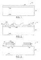
- Figure 1 illustrates an LED device precursor 10 according to some embodiments of the present invention, comprising a substrate 20 having first and second opposing faces 20a and 20b, respectively, and an epitaxial region 22 formed on the first face 20a of the substrate 20.
- Substrate 20 may comprise silicon carbide, sapphire, aluminum nitride, gallium nitride or any other suitable conductive or non-conductive substrate material.
- the substrate 20 comprises conductively doped SiC.
- the substrate 20 is transparent to optical radiation in a predetermined wavelength range.
- epitaxial region 22 comprises a conductive buffer layer and a plurality of Group III-nitride epitaxial layers, at least some of which provide a diode region.
- the dimensions of the substrate, epitaxial layers and metal layers shown in Figures 1-10 are not drawn to scale but are exaggerated for illustrative purposes.
- a thin SiO 2 and/or other layer may optionally be formed, for example, by Plasma Enhanced Chemical Vapor Deposition (PECVD) on the surface of the epitaxial region 22 to protect it during subsequent processing and cleaning steps.
- PECVD Plasma Enhanced Chemical Vapor Deposition
- the epitaxial region 22 is patterned as shown in Figure 2 to form a plurality of mesas 30 each having sidewalls 30a, 30b.
- the mesas 30 may extend into the substrate 20.
- the mesas 30 may be formed by selective epitaxial growth through openings in a mask, rather than blanket epitaxial growth and etching.
- a layer of photoresist 24 and/ or other material is formed on the surface of the precursor 10 and patterned to expose the surface of the mesas 30, thereby defining a first reduced area 30c on the surface of the mesas 30. If an optional SiO 2 layer is present, it may be etched through the openings in the photoresist 24 to expose the first reduced area 30c on the epitaxial surface layer of the epitaxial region 22 in the mesa 30.
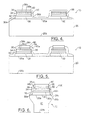
- a multilayer conductive stack 35 is then formed on the first reduced areas 30c of the mesas 30 using, for example, conventional lift-off techniques.
- the multilayer conductive stack 35 includes an ohmic layer 32, a reflector layer 34 and a barrier layer 36.
- the ohmic layer 32 comprises platinum, but in other embodiments it may comprise palladium, nickel/gold, nickel oxide/gold, nickel oxide/platinum, titanium and/or titanium/gold. Other embodiments of ohmic layers are described in the above-referenced U.S. Publication No. US 2002/0123164 A1 . If the ohmic layer 32 comprises Pt, it is about 25 ⁇ thick in some embodiments of the present invention.
- the reflector layer 34 may comprise any suitable reflective metal, and may comprise Al or Ag.
- the reflector layer 34 is about 1000 ⁇ thick in some embodiments of the present invention.
- Other embodiments of reflector layers are described in the above-referenced Application Serial No. 10/057,821 , corresponding to U.S. Publication No. US 2002/0123164 A1 .
- the barrier layer 36 can be a solder barrier layer to prevent solder metals such as tin from reacting with the reflector layer 34 and/or ohmic layer 32.
- the barrier layer 36 comprises W, TiW and/or TiN/W and is between about 500 ⁇ and about 50,000 ⁇ thick in some embodiments of the present invention, and is about 5000 ⁇ thick in other embodiments of the present invention.
- the barrier layer 36 may comprise TiW having a composition of about 5% Ti and about 95% W.
- barrier layer 36 that comprise tungsten or titanium/tungsten and that are between about 500 ⁇ thick to about 3000 ⁇ thick, may be used when a solder bonding operation (described below) is performed at a reflow temperature of less than about 210°C.
- a solder bonding operation (described below) is performed at a reflow temperature of less than about 210°C.
- a barrier layer comprising between about 500 ⁇ and about 3000 ⁇ of titanium/tungsten may be used, according to some embodiments of the present invention.
- the barrier layer 36 comprises a first layer of tungsten or titanium/tungsten 36a that is about 5000 ⁇ thick, and a second layer 36b comprising nickel that is about 2000 ⁇ thick, on the first layer, 36a.
- a multilayer barrier layer 36 comprising a layer of tungsten or titanium/tungsten 36a and a layer of nickel 36b is used with solders that have a reflow temperature of more than about 200°C.
- these multilayer barrier layers may be used with solders that have a reflow temperature of more than about 250°C.
- tungsten, silver and platinum are deposited, for example, using an e-beam technique.
- TiW may be deposited using an e-beam technique, but in other embodiments of the present invention, Ti and W are simultaneously sputter deposited.
- the TiW may be sputter deposited in the presence of nitrogen to form a TiN/TiW layer that also forms a barrier to Sn diffusion, in other embodiments of the present invention.
- the barrier layer 36 may consist essentially of nickel or NiV.
- the barrier layer 36 may comprise a 2500 ⁇ nickel solder barrier covered completely with a layer of gold between about 500 ⁇ and 10,000 ⁇ thick.
- the gold layer can prevent the nickel layer from oxidizing.
- the use of a nickel barrier layer may result in unacceptably high degradation of optical and electrical performance at elevated temperature and current levels due to tin migration.
- thicker films of nickel may be difficult to use since the film stress may be high. This may create concern with respect to delamination of the nickel from the adjacent reflective and/or ohmic layers.
- the presence of Au at the edges of the barrier layer may create a path for Sn to migrate down and around the edges of the barrier.
- a passivation layer 40 is deposited or otherwise formed on the first (or epitaxial-side) surface 20a of device precursor 10.
- passivation layer 40 may comprise SiO 2 and/or SiN (which may be deposited in stoichiometric or non-stoichiometric amounts) and may be deposited by conventional techniques such as PECVD and/or reactive sputtering.
- the passivation layer 40 is about 1500 ⁇ thick in some embodiments of the present invention.
- this blanket deposition also forms the passivation layer on the sidewalls of the mesas 30 and the multilayer conductive stack 35, and on the exposed surface of the barrier layer 36.
- the passivation layer 40 is patterned with an etch mask (such as a photoresist) to provide a first patterned passivation layer 40a and to selectively reveal a second reduced area portion 36c of the surface of barrier layer 36.
- an etch mask such as a photoresist
- a lift off technique may be used to expose the second reduced area portion 36c of the surface of the barrier layer 36.
- selective deposition of the passivation layer 40a may be used so that a separate patterning step need not be used.
- an optional adhesion layer 55 comprising, for example, Ti is then deposited on the second reduced area 36c of the barrier layer 36 and a bonding layer 60 is deposited on the adhesion layer 55.
- the adhesion layer 55 is about 1000 ⁇ thick in some embodiments of the present invention.
- the bonding layer 60 may comprise Au, Sn and/or AuSn and is about 1000 ⁇ thick in some embodiments.
- the bonding layer 60 may be up to about 1 ⁇ m thick (if Au) or about 1.7 ⁇ m thick (if AuSn) in some embodiments of the present invention.
- the patterned passivation layer 40a also is on the sidewalls of the adhesion layer 55 and the bonding layer, according to some embodiments of the present invention. In other embodiments, the patterned passivation layer 40a does not extend on the sidewalls of the adhesion layer 55 and the bonding layer 60. In these embodiments, the passivation layer may extend on the sidewalls of the conductive stack 35.
- the bonding layer 60 extends away from the multilayer conductive stack 35, to beyond the patterned passivation layer 40a. In yet other embodiments, the bonding layer 60 does not extend to beyond the outer surface of the patterned passivation layer 40a.
- ohmic contacts and a wire bond pad are formed on the second substrate face 20b opposite the epitaxial region to form a vertically-conductive device.
- Many such embodiments are described in Application Serial No. 10/057,821 , corresponding to U.S. Publication No. US 2002/0123164 A1 .
- ohmic contacts and metal bonding layers may be formed on an n-type epitaxial region of the device to form a horizontally-conductive device.
- Many such embodiments also are shown in Application Serial No. 10/057,821 , corresponding to U.S. Publication No. US 2002/0123164 A1 .
- the precursor 10 is diced into individual light emitting diodes 100.
- Figure 6 also shows that LEDs 100 may be sawed such that they have a beveled sidewall configuration 70 to increase light extraction.
- substrate shaping are described in Application Serial No. 10/057,821 , corresponding to U.S. Publication No. US 2002/0123164 A1 .
- Figure 6 illustrates light emitting diodes 100 according to some embodiments of the present invention that include a substrate 20, an epitaxial region (referred to previously as a mesa) 30 on the substrate 20 that includes therein a diode region, a multilayer conductive stack 35 on the epitaxial region 30 opposite the substrate 20, and a passivation layer 40b that extends at least partially on the multilayer conductive stack 35 opposite the epitaxial region 30, to define a reduced area bonding region 36c on the multilayer conductive stack 35 opposite the epitaxial region 30.
- the passivation layer 40b also extends across the multilayer conductive stack 35, across the epitaxial region 30, and onto the first substrate face 20a.
- the multilayer conductive stack 35 and the epitaxial region 30 both include sidewalls, and the passivation layer 40b extends on the sidewalls of the multilayer conductive stack 35 and of the epitaxial region 30.
- a bonding layer 60 is provided on the bonding region 36c.
- the bonding layer 60 also includes a bonding layer sidewall, and the passivation layer 40b may or may not extend onto the bonding layer sidewall.
- an adhesion layer 55 may be provided between the multilayer conductive stack 35 and the bonding layer 60, and the passivation layer 40b also may or may not extend onto the sidewall of the adhesion layer 55 and/or the bonding layer 60.
- the substrate 20 includes a first face 20a adjacent the epitaxial region 30 and a second face 20b opposite the epitaxial region.
- the bonding layer 60 has smaller surface area than the multilayer conductive stack 35 and the multilayer conductive stack 35 has smaller surface area than the epitaxial region 30.
- the epitaxial region 30 has smaller surface area than the first face 20a.
- the second face 20b also has smaller surface area than the first face 20a.
- Figure 6 also illustrates light emitting diodes according to some embodiments of the invention that include a substrate 20 having first and second opposing faces 20a and 20b, respectively, the second face 20b having smaller surface area than the first face.
- An epitaxial region 30 is on the first face 20a, and includes therein a diode region.
- An ohmic layer 32 is on the epitaxial region 30 opposite the substrate 20.
- a reflector layer 34 is on the ohmic layer 32 opposite the epitaxial region 30.
- a barrier layer 36 is on the reflector layer 34 opposite the ohmic layer 32.
- An adhesion layer 55 is on the barrier layer 36 opposite the reflector layer 34.
- a bonding layer 60 is on the adhesion layer 55 opposite the barrier layer 36.
- the barrier layer 36 comprises tungsten, titanium/tungsten and/or titanium nitride/tungsten.
- the tin barrier layer 36 comprises a first layer 36a comprising tungsten and a second layer 36b comprising nickel on the first layer 36a comprising tungsten.
- the epitaxial region 30 has smaller surface area than the first face 20a.
- the barrier layer 36, the reflector layer 34 and the ohmic layer 32 have same surface area, that surface area being less than that of the epitaxial region 30.
- the adhesion layer 55 and the bonding layer 60 have same surface area, that surface area being smaller than that of the barrier layer 36, the reflector layer 34 and the ohmic layer 32.
- the epitaxial region 30, the ohmic layer 32, the reflector layer 34, the barrier layer 36, the adhesion layer 55 and the bonding layer 60 each include a sidewall and the light emitting diode 100 further includes a passivation layer 40b on the sidewalls of the epitaxial region 30, the ohmic layer 32, the reflector layer 34 and the barrier layer 36.
- the passivation layer also may or may not extend onto the sidewalls of the adhesion layer 55 and/or the bonding layer 60.
- the passivation layer 40b also may extend on the first face 20a of the substrate 20.
- Figure 7 illustrates other embodiments of the present invention in which the bonding layer 60 comprises a solder wetting layer 62 and a wetting passivation layer 64.
- the solder wetting layer 62 comprises nickel and is about 2000 ⁇ thick.
- the wetting passivation layer 64 comprises Au and is about 500 ⁇ thick.
- Use of the nickel solder wetting layer 62 can provide an enhanced mechanical bond to the solder, which can increase the shear strength of the connection and can reduce the possibility of mechanical failure, according to some embodiments of the invention.
- Figure 8 illustrates other embodiments of the present invention in which the bonding layer 60 and optional adhesion layer 55 do not extend beyond the outer edge 40c of the passivation layer 40b. This configuration may be used when solder bonding is used to mount the LED to a lead frame, according to some embodiments of the invention.
- Figures 1-8 also illustrate methods of fabricating a plurality of light emitting diodes according to some embodiments of the present invention. These methods comprise epitaxially forming a plurality of spaced apart mesa regions 30 on a substrate 20, the mesa regions including therein a diode region ( Figure 2 ). A first reduced area region 30c is defined on the mesa regions ( Figure 2 ). A multilayer conductive stack 35 that includes a barrier layer, is formed on the first reduced area regions 30c of the mesa regions 30 ( Figure 3 ).
- a passivation layer 40a is formed on the substrate 20 between the mesa regions 30, on exposed portions of the mesa regions and on exposed portions of the multilayer stack 35, the passivation layer 40a defining a second reduced area region 36c on the multilayer conductive stack 35 ( Figures 4 and 5 ).
- a bonding layer 60 then is formed on the second reduced area regions 36c of the multilayer conductive stacks 35 ( Figure 5 ).
- the substrate 20 is diced between the mesas 30 to produce the plurality of light emitting diodes 100 ( Figure 6 ).
- Figure 9 illustrates embodiments of the present invention in which the LED 100 is mounted in a "flip-chip" configuration with the epitaxial side down, via thermosonic and/or thermocompression bonding. That is, instead of using an epoxy or a solder to form a mechanical connection or bond between the LED 100 and the submount 75, the bonding layer 60 of LED 100 is thermosonically or thermocompressively bonded directly to the submount 75 as described, for example, in United States Provisional Application Serial No. 60/307,234 and U.S. Publication No. US 2003/0042507 A1 .
- thermosonic or thermocompression bonding the LED chip 100 is placed into mechanical contact with the submount and subjected to mechanical and/or sonic stimulation at a temperature greater than the eutectic temperature of the bonding metal.
- the bonding metal thus forms a bond with the metallic submount, which provides an electromechanical connection between the LED and the submount.
- the temperature used for thermosonic bonding may be approximately 300 °C.
- barrier layer 36 and/or the passivation layer 40b can reduce or prevent unwanted interaction between metals in the bonding layer 60 with the reflective layer 34 and/or the ohmic layer 32.
- the barrier layer 36 and/or the passivation layer 40 may also serve to retard or inhibit unwanted migration of metal along the edge of the metal stack 35.
- the LED 100 may be mounted on the submount 75 using a metal solder 80 such as SnAg, SnPb and/or other solders as illustrated in Figure 10 .
- the passivation layer 40b can reduce or prevent Sn from solder 80 from migrating to (and thereby potentially degrading) the reflective layer 34 and/or ohmic layer 32.
- the passivation layer 40b also can reduce or prevent conductive solder 80 from contacting the substrate 20 and mesa sidewalls, which may otherwise result in the formation of unwanted parasitic Schottky contacts to n-type regions of the device 100.
- Other bonding techniques that may be used, according to other embodiments of the present invention, are disclosed in the above-cited Provisional Application Serial No. 60/307,311 and U.S. Publication No. 2003/0045015 A1 .
- test results are illustrative and shall not be construed as limiting the scope of the present invention.
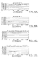
- Figures 11A-11D graphically illustrate test results for a 2500 ⁇ Ni solder barrier while Figures 12A-12D graphically illustrate results for a 5000 ⁇ TiW barrier.
- HTOL high temperature operating life
- the devices with the Ni barrier exhibited larger degradation in light output, compared to the devices with the TiW barrier. Moreover, V F increased more in the Ni barrier devices ( Figure 11B ) than in the TiW barrier devices ( Figure 12B ).
- the reflector layer 34 also referred to as a mirror 34
- metal can short circuit the pn junction of the device if it comes into contact with the mesa 30.
- the mirror 34 comprises silver, which tends to migrate easily at relatively low temperatures. See, for example, the textbook entitled Corrosion and Environmental Degradation, Vol. II, to Schütze, 2000, pp. 451-452 .
- silver ions can form at positive (anodic) metallizations due to oxidation and/or corrosion.
- the silver ions migrate to negative (cathodic) metallizations, they can plate out in the form of a dendrite (i.e., a branching structure).
- the dendrite may eventually bridge the gap between the anode and cathode of the LED and cause a short circuit.
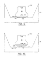
- barrier layer 36 may be desirable to extend the barrier layer 36 over the sidewalls of the reflector layer 34, as illustrated in Figure 13 . This may be accomplished by performing an additional photolithography step to form the ohmic contact layer 32 and the reflector layer 34 to have a reduced width compared to the width of barrier layer 36, and/or using other conventional techniques. Thus, when barrier layer 36 is formed, e.g., deposited, it may contact the sidewalls of reflector layer 34 and ohmic contact 32 as well as a portion of the surface of mesa 30 surrounding the ohmic contact 32 and reflector layer 34.
- the barrier layer 36 is formed in such a way as to cover the sidewalls of reflector layer 34 as illustrated in Figure 13 , it is possible for cracks in the barrier layer to form near the sidewalls of the reflector layer 34. Such cracks may provide a migration path for silver from the reflector layer 34 to escape and potentially migrate to the mesa 30.
- the formation of cracks is illustrated in Figure 14 , which shows a mesa 30 on which a thin ohmic contact layer 32 has been formed.
- a silver reflector layer 34 is formed on the ohmic contact layer 32, and the entire structure is covered with a layer 36 of a barrier metal such as TiW.
- the TiW barrier metal layer 36 when the TiW barrier metal layer 36 is deposited, it forms vertically oriented grains 47 separated by grain boundaries 49. Misalignment of the grains 47 at the corners of the reflector layer 34 may cause cracks 51 to form, which may provide a migration path for metal from the reflector layer 34 to escape and potentially migrate to the mesa 30.
- a barrier layer 36 may comprise a plurality of alternating sublayers of a barrier metal 36A such as TiW and a second metal 36B such as platinum, as illustrated in Figure 15 .
- Suitable metals for second metal 36B are Pt, Ti, Ni and/or other metals.
- Metal 36B should not be susceptible to migration in the LED structure and should have a melting point higher than any of the processing steps subsequently used in the fabrication of the LED (in some embodiments at least about 200°C).
- barrier layer 36 comprises alternating sublayers of about 1000 ⁇ of TiW and about 500 ⁇ of platinum repeated at least two times with the top and bottom sublayers of the stack both comprising TiW.
- the plurality of first and second alternating sublayers define first and second outer sublayers that comprise the first sublayer.
- the second (final) outer layer of TiW in the stack may be made approximately 5000 ⁇ thick to act as a solder barrier.
- the TiW/Pt layer stacks are repeated six times with the final (terminating) layer of TiW being about 5000 ⁇ thick.
- Many other thicknesses of the barrier metal 36A and the second metal 36B may be used in other embodiments of the invention.
- barrier metal 36A should be sufficiently thin to reduce or prevent cracking, but sufficiently thick to provide an effective barrier, while the second metal 36B should be sufficiently thin so as not to degrade the resistance of the contact, but sufficiently thick to prevent cracks in the barrier metal layer 36A from propagating across the second barrier layer.
- the grain boundaries 49 of successive layers of TiW do not necessarily align vertically, thereby inhibiting the formation of long cracks through the barrier layer 36 that may otherwise provide a migration path for the reflector metal.
- the successive TiW layers may form a pattern that generally resembles a brick wall with stacks of offset grains in each layer.
- FIGs 16 and 17 are 40,000X SEM images of a metal stack fabricated in accordance with the embodiments illustrated in Figures 14 and 15 , respectively.
- a TiW barrier layer 36 is deposited as a single layer over a reflector 34 and ohmic contact 32.
- Vertical grain boundaries 49 are visible within the barrier layer 36.
- a crack 51 is visible extending from the edge of the reflector layer 34 to the surface of the barrier layer.
- the barrier layer 36 comprises a plurality of alternating layers of TiW 36A and platinum 36B.
- the grain boundaries 49 in the alternating layers of TiW 36A can be clearly seen to form a brick wall pattern over the reflector layer 34 and mesa 30.
- no cracking is evident in the barrier layer 36.
Landscapes
- Led Devices (AREA)
- Electrodes Of Semiconductors (AREA)
- Led Device Packages (AREA)
Abstract
Description
- This invention relates to microelectronic devices and fabrication methods therefor, and more particularly to light emitting devices, such as light emitting diodes (LEDs) and manufacturing methods therefor.
- Light emitting diodes are widely used in consumer and commercial applications. As is well known to those having skill in the art, a light emitting diode generally includes a diode region on a microelectronic substrate. The microelectronic substrate may comprise, for example, gallium arsenide, gallium phosphide, alloys thereof, silicon carbide and/or sapphire. Continued developments in LEDs have resulted in highly efficient and mechanically robust light sources that can cover the visible spectrum and beyond. These attributes, coupled with the potentially long service life of solid state devices, may enable a variety of new display applications, and may place LEDs in a position to compete with the well entrenched incandescent and fluorescent lamps.
- Gallium Nitride (GaN)-based LEDs typically comprise an insulating or semiconducting substrate such as silicon carbide (SiC) or sapphire on which a plurality of GaN-based epitaxial layers are deposited. The epitaxial layers comprise an active or diode region having a p-n junction which emits light when energized.
- LEDs may be mounted substrate side down onto a submount, also called a package or lead frame (hereinafter referred to as a "submount"). In contrast, flip-chip mounting of light emitting diodes involves mounting the LED onto the submount with the substrate side facing up (i.e. away from the submount). Light may be extracted and emitted through the substrate. Flip chip mounting may be an especially desirable technique for mounting SiC-based LEDs. In particular, since SiC has a higher index of refraction than GaN, light generated in the active or diode region generally does not totally internally reflect (i.e. reflect back into the GaN-based layers) at the GaN/SiC interface. Flip chip mounting of SiC-based LEDs also can improve the effect of certain substrate-shaping techniques known in the art. Flip chip packaging of SiC LEDs may have other benefits, such as improved heat dissipation, which may be desirable depending on the particular application for the LED.
- Because of the high index of refraction of SiC, light passing through an SiC substrate tends to be totally internally reflected into the substrate at the surface of the substrate unless the light strikes the surface at a fairly low angle of incidence (i.e. fairly close to normal). The critical angle for total internal reflection generally depends on the material with which SiC forms an interface. It is possible to increase the light output from an SiC-based LED by shaping the SiC substrate in a manner that limits total internal reflection by causing more rays to strike the surface of the SiC at low angles of incidence. A number of such shaping techniques and resulting devices are taught in
U.S. Patent Application Serial No. 10/057,821 to Slater et al , corresponding to U.S. Publication No.US 2002/0123164 A1, published September 5, 2002 , entitled Light Emitting Diodes Including Modifications for Light Extraction and Manufacturing Methods Therefor. - One potential problem with flip-chip mounting is that when an LED is mounted on a submount using conventional techniques, a conductive die attach material such as silver epoxy is deposited on the LED and/or on the package, and the LED and the submount are pressed together. This can cause the viscous conductive die attach material to squeeze out and make contact with the N-type substrate and/or layers in the device, thereby forming a Schottky diode connection that can short-circuit the p-n junction in the active region.
- Metal-metal bonds formed by soldering, thermosonic scrubbing and/or thermocompression bonding are alternative attach techniques. However, tin (Sn) is a component of most types of solder, and migration of Sn from the bonded surface into the device can cause unwanted degradation of the device. Such migration can interfere with metal-semiconductor interfaces such as ohmic contacts and/or the function of metal-metal interfaces such as reflective interfaces that serve as mirrors.
- Semiconductor light emitting devices such as light emitting diodes, according to some embodiments of the present invention, include a substrate, an epitaxial region on the substrate that includes therein a light emitting region such as a light emitting diode region, and a multilayer conductive stack comprising a reflector layer including a reflector layer sidewall, on the epitaxial region. A barrier layer is provided on the reflector layer and extending on the reflector layer sidewall. In other embodiments, the multilayer conductive stack further comprises an ohmic layer, including an ohmic layer sidewall, between the reflector and the epitaxial region. The barrier layer further extends on the ohmic layer sidewall. In still other embodiments of the present invention, the barrier layer further extends onto the epitaxial region outside the multilayer conductive stack.
- In other embodiments of the present invention, the barrier layer comprises a plurality of first and second alternating sublayers. In some embodiments, the first sublayers include grain boundaries therein and the second sublayers are substantially free of grain boundaries. In other embodiments, the first sublayers include grain boundaries that are arranged such that the grain boundaries define an offset brick wall structure of the first sublayers. In still other embodiments, the first sublayers comprise titanium tungsten and the second sublayers comprise platinum, titanium and/or nickel.
- In some embodiments, the first sublayers are configured to reduce migration of metal from the reflector layer, and the second sublayers are configured to prevent at least some grain boundaries in the first sublayers for propagating thereacross. In other embodiments, the plurality of first and second alternating sublayers define first and second outer sublayers that comprise the first sublayer. In still other embodiments, the second outer sublayer is thicker than the first outer sublayer.
- Other embodiments of the invention provide methods of reducing migration of metal from the reflective layer into the epitaxial region of a semiconductor light emitting device, by forming a barrier layer on the reflector layer that extends on the reflector layer sidewall. In other embodiments, the barrier layer is formed to extend on the ohmic layer sidewall. In still other embodiments, the barrier layer extends onto the epitaxial region outside the multilayer conductive stack.
- Still other embodiments of the present invention form the barrier layer as a plurality of alternating first and second sublayers, which can reduce cracking of the barrier layer adjacent the reflector layer sidewall. The first and second sublayers can define an offset brick wall structure that can terminate with a first sublayer, to define an outer sublayer, wherein the second sublayers are thinner than the first sublayers and the outer sublayer is thicker than the first sublayers.
-
-
Figures 1-10 are cross-sectional views of light emitting diodes according to some embodiments of the present invention during intermediate fabrication steps according to some embodiments of the present invention. -
Figures 11A-12D graphically illustrate test results for light emitting diodes according to some embodiments of the present invention. -
Figures 13-15 are cross-sectional views of light emitting diodes according to other embodiments of the present invention. -
Figures 16 and 17 are SEM images of light emitting diodes according to other embodiments of the present invention. - The present invention now will be described more fully hereinafter with reference to the accompanying figures, in which embodiments of the present invention are shown. This invention may, however, be embodied in many alternate forms and should not be construed as limited to the embodiments set forth herein.
- Accordingly, while the present invention is susceptible to various modifications and alternative forms, specific embodiments thereof are shown by way of example in the drawings and will herein be described in detail. It should be understood, however, that there is no intent to limit the present invention to the particular forms disclosed, but on the contrary, the present invention is to cover all modifications, equivalents, and alternatives falling within the spirit and scope of the present invention as defined by the claims. Like numbers refer to like elements throughout the description of the figures. In the figures, the dimensions of layers and regions may be exaggerated for clarity. It will also be understood that when an element, such as a layer, region or substrate, is referred to as being "on" another element, it can be directly on the other element or intervening elements may also be present. In contrast, when an element, such as a layer, region or substrate, is referred to as being "directly on" another element, there are no intervening elements present. Moreover, each embodiment described and illustrated herein includes its complementary conductivity type embodiment as well.
- Embodiments of the present invention now will be described generally with reference to gallium nitride-based light emitting diodes on silicon carbide-based substrates. However, it will be understood by those having skill in the art that many embodiments of the present invention may employ any combination of a substrate that is non-absorbing or transparent to the emitted light and an index matched light emitting diode epitaxial layer. In some embodiments of the present invention, the refractive index of the substrate is greater than that of the diode. Accordingly, combinations can include an AlGaInP diode on a GaP substrate; an InGaAs diode on a GaAs substrate; an AlGaAs diode on a GaAs substrate; an SiC diode on an SiC substrate, an SiC diode on a sapphire (Al2O3) substrate; and/or a nitride-based diode on a gallium nitride, silicon carbide, aluminum nitride, zinc oxide and/or other substrate. Finally, it will be understood that although embodiments of the present invention are described herein with respect to light emitting diodes having an epitaxial region that includes therein a light emitting diode region, other embodiments of the present invention may be used with other semiconductor light emitting devices such as lasers, wherein an epitaxial region includes therein a light emitting region such as a laser diode region.
- Some embodiments of the present invention provide a metal stack with a passivation layer on its perimeter that defines a bonding region on LED devices that can be well suited for die attachment via soldering and/or thermosonic scrub bonding. Other embodiments of the present invention provide LED devices that can be flip chip mounted using soldering and/or thermosonic bonding, and that include a barrier layer that can reduce or eliminate unwanted degradation of the metal and/or semiconductor layers of the LED. Still other embodiments of the present invention can provide both the passivation layer and the barrier layer. Yet other embodiments of the present invention provide methods of fabricating these LED devices. Passivation layers according to some embodiments of the present invention can provide means for preventing a short circuit across the diode region. Moreover, barrier layers according to some embodiments of the present invention can provide means for reducing migration of tin and/or other undesired materials into the LED.
- In a conventional sapphire-based approach, an LED, also referred to as a chip or die, is attached to a submount with a clear epoxy. In the case of LEDs having conductive SiC substrates, a conducting silver filled epoxy is typically used to attach the LED and the submount to one another. Conventional nitride-based LEDs on SiC or sapphire substrates generally are packaged with the epitaxial side up and with the substrate bonded to the submount.
- Some embodiments of conventional SiC-based LEDs have an n-type conductive substrate and an epitaxial region on the substrate that includes one or more n-type epitaxial layers and one or more p-type epitaxial layers to define a diode region. A transparent ohmic contact may be formed on the p-type epitaxial LED surface. As discussed in
U.S. Patent Application Serial No. 10/057,821 , corresponding to U.S. Publication No.US 2002/0123164 A1 , referenced above, it may be beneficial to form a reflector layer over the thin transparent ohmic contact to improve light extraction from the device. The reflective layer can serve to spread electric current uniformly across the thin contact, and also to reflect light back into the substrate, away from the submount. - Unfortunately, if Sn and/or other contaminants from a solder or thermosonic/thermocompression bond migrates from the bonding surface to the reflector layer, the reflector layer may become less reflective. Moreover, if the contaminants migrate beyond the reflector to the transparent ohmic contact, the transparent ohmic contact may develop a higher specific contact resistivity, thus increasing the forward voltage (VF) of the device. Both of these results may be characterized as degradation of the device.
- A reflective layer may comprise Ag and/or Al, and the thin transparent ohmic layer can comprise Pt, Pd, Ni, Ti, Au or a combination of these elements. Unfortunately, Sn readily forms alloys with Ag, Pt, Au and with numerous other metals used in semiconductor manufacturing.
- A first portion of a series of conductive layers (referred to herein as a "multilayer conductive stack") that may be formed on the p-type surface of an LED according to some embodiments of the present invention comprises an ohmic layer, a reflector layer, and a barrier layer. In some embodiments, the barrier layer comprises a thin layer of titanium, titanium/tungsten (TiW) and/or titanium nitride/tungsten (TiNW). In other embodiments, the barrier layer comprises a first layer of titanium/tungsten and a second layer comprising nickel on the first layer. In still other embodiments, the barrier layer extends onto the sidewalls of the ohmic layer and the reflector layer and/or includes an alternating stack of a barrier metal layer and a second metal.
- In some embodiments of the present invention, this portion of the multilayer conductive stack and the top of the device are passivated with a passivation layer, such as an insulating layer to which a solder or eutectic die attach material will not wet. The passivation layer can be formed by conventional spin-on or deposition techniques such as Chemical Vapor Deposition (CVD) and/or reactive sputtering, and it can comprise an insulating oxide and/or nitride such as silicon dioxide and/or silicon nitride.
- In some embodiments of the present invention, an opening in the passivation layer is then formed with lateral dimensions (i.e. surface area) that are smaller than the lateral dimensions of the barrier layer such that only a portion of the surface of the barrier layer is exposed. Such an opening can be produced using conventional photolithography and etching techniques. An optional adhesion layer that may comprise Ti, is formed in the opening and a thick bonding layer that may comprise Au, Sn and/or AuSn also is formed. In other embodiments, an optional solder wetting layer is provided between the adhesion layer and the bonding layer. The solder wetting layer can provide an enhanced mechanical connection between the solder and the LED, which can increase the shear strength of the connection.
- In some embodiments of the present invention, the bonding layer can serve to protect the barrier layer if mechanical stress is to be applied to the multilayer conductive stack by a probe tip during electrical tests. Furthermore, in other embodiments of the present invention, the Au in the bonding layer can serve to protect the barrier layer from oxidation. In yet other embodiments of the present invention, AuSn may be employed in the bonding layer as a eutectic die attach material that may be used to bond an LED and a submount to one another via thermosonic or thermocompression bonding as an alternative to solder bonding.
- Multilayer conductive stacks according to some embodiments of the present invention can be well suited for solid state devices in that some embodiments of the present invention can provide a stack that is considerably thinner than may be achieved if a solder barrier is formed using Ni or NiV. In some embodiments of the present invention, a barrier layer comprising W, TiW and/or TiNW and/or W and Ni layers can be less than half of the thickness that may be used if only Ni were used as the barrier layer. This may be advantageous when considering the generally small lateral dimensions of solid state devices and when considering the potential difficulty associated with the use of conventional fabrication techniques if large topographical dimensions are present. The barrier layer also can provide a desired vertical barrier against Sn and/or other undesired migration.
- Passivation layers according to some embodiments of the invention can cover the entire epitaxial surface of the LED except for a reduced area opening that exposes the barrier layer, and can provide a dam to reduce or prevent Sn and/or other undesired migration into the reflective mirror layer or the ohmic contact, or down the edges of the metal stack. In the case of an LED having a conducting substrate, passivation layers according to some embodiments of the invention also can serve to keep the die attach material from contacting the substrate which could produce undesired effects such as formation of a parasitic Schottky diode.
- Large area LEDs operating at high power levels may use packaging that has low thermal resistance to reduce or prevent degradation of the device performance. Epoxy based die attach materials may have high thermal resistance in comparison to metal die attach materials. In a flip-chip configuration, the p-n junction region of an LED is mounted extremely close to the heat sinking package, which can bypass the thermal resistance of the substrate. This may be used for large-area SiC-based LEDs in some embodiments of the present invention, despite the low thermal resistance of SiC. The metal-metal bond provided by some embodiments of the present invention also may be used in LEDs having sapphire substrates, due to the high thermal resistance of sapphire. Consequently, some embodiments of the present invention may be used for large area LEDs, which may benefit from employing a junction down (flip-chip) metal-metal die attach configuration. Other embodiments of the present invention may be used with small-area LEDs.
- Some embodiments of the present invention also may increase the permissible temperature range that the device can withstand during subsequent packaging, assembly and re-work/repair steps. Metal-metal bonds can be engineered for subsequent thermal cycles, for example, where the LED is mounted to a printed circuit board. If the LED die is attached to its submount with a AuSn thermosonic or thermocompression bond at 300°C or by SnAg solder at 230°C, subsequent processing cycles using SnPb solder at 200°C may not cause mechanical failure by reflowing the die attach bond. That is, subsequent processing at elevated temperatures may not cause the LED die to detach from the submount. In contrast, LEDs using epoxy based die attach methods may not withstand high thermal cycles. Moreover, clear epoxy can become discolored during thermal processing, resulting in unwanted light attenuation.
- Some embodiments of the present invention may also increase the shear strength of resulting bonds between the LED and the submount. Inclusion of a solder barrier layer which reduces or prevents tin and/or other unwanted materials from reaching the epitaxial layers of the device can preserve the adhesive strength of the metal-semiconductor interface and can result in a more robust, mechanically stable device. In particular, it has been found that embodiments that include a nickel solder wetting layer beneath a gold bonding layer may exhibit superior shear strength. The shear strength may also be maintained through thermal cycles during subsequent packaging, assembly and re-work/repair steps.
- In addition, some embodiments of the present invention may improve the thermal conductivity of the resulting device. This effect may be particularly apparent in so-called "power" or large area LEDs which may carry a substantially higher current than conventional LEDs. In such LEDs, some embodiments of the present invention can prevent or reduce "voiding" within the metallic layers. Voiding refers to the formation of physical voids or spaces within a metallic region. Some embodiments of the present invention may serve to maintain a tight grain structure within such metallic layers, thereby allowing the device to maintain a high thermal conductivity despite operation at high power levels with correspondingly high junction temperatures. Improved thermal conductivity also may help reduce degradation of encapsulant materials in which LEDs, and in particular power LEDs, are packaged. Such encapsulants are typically sensitive to heat and may yellow and become less transparent after expose to high temperatures for extended periods of time. By improving the thermal conductivity of the LED mount interface, less heat may be dissipated through the encapsulant, which can result in reduced degradation.
-
Figure 1 illustrates anLED device precursor 10 according to some embodiments of the present invention, comprising asubstrate 20 having first and second opposing faces 20a and 20b, respectively, and anepitaxial region 22 formed on thefirst face 20a of thesubstrate 20.Substrate 20 may comprise silicon carbide, sapphire, aluminum nitride, gallium nitride or any other suitable conductive or non-conductive substrate material. In some embodiments of the present invention, thesubstrate 20 comprises conductively doped SiC. In some embodiments of the present invention, thesubstrate 20 is transparent to optical radiation in a predetermined wavelength range. In some embodiments of the present invention,epitaxial region 22 comprises a conductive buffer layer and a plurality of Group III-nitride epitaxial layers, at least some of which provide a diode region. The dimensions of the substrate, epitaxial layers and metal layers shown inFigures 1-10 are not drawn to scale but are exaggerated for illustrative purposes. A thin SiO2 and/or other layer (not shown) may optionally be formed, for example, by Plasma Enhanced Chemical Vapor Deposition (PECVD) on the surface of theepitaxial region 22 to protect it during subsequent processing and cleaning steps. - Subsequent to deposition of the
epitaxial region 22, theepitaxial region 22 is patterned as shown inFigure 2 to form a plurality ofmesas 30 each havingsidewalls Figure 2 , themesas 30 may extend into thesubstrate 20. Moreover, in some embodiments of the present invention, themesas 30 may be formed by selective epitaxial growth through openings in a mask, rather than blanket epitaxial growth and etching. - Still referring to
Figure 2 , in some embodiments of the present invention, a layer ofphotoresist 24 and/ or other material is formed on the surface of theprecursor 10 and patterned to expose the surface of themesas 30, thereby defining a first reducedarea 30c on the surface of themesas 30. If an optional SiO2 layer is present, it may be etched through the openings in thephotoresist 24 to expose the first reducedarea 30c on the epitaxial surface layer of theepitaxial region 22 in themesa 30. - A multilayer
conductive stack 35 is then formed on the first reducedareas 30c of themesas 30 using, for example, conventional lift-off techniques. As shown inFigure 3 , the multilayerconductive stack 35 includes anohmic layer 32, areflector layer 34 and abarrier layer 36. In some embodiments of the present invention, theohmic layer 32 comprises platinum, but in other embodiments it may comprise palladium, nickel/gold, nickel oxide/gold, nickel oxide/platinum, titanium and/or titanium/gold. Other embodiments of ohmic layers are described in the above-referenced U.S. Publication No.US 2002/0123164 A1 . If theohmic layer 32 comprises Pt, it is about 25Å thick in some embodiments of the present invention. Thereflector layer 34 may comprise any suitable reflective metal, and may comprise Al or Ag. Thereflector layer 34 is about 1000Å thick in some embodiments of the present invention. Other embodiments of reflector layers are described in the above-referenced Application Serial No.10/057,821 US 2002/0123164 A1 . - In some embodiments of the present invention, the
barrier layer 36 can be a solder barrier layer to prevent solder metals such as tin from reacting with thereflector layer 34 and/orohmic layer 32. Thebarrier layer 36 comprises W, TiW and/or TiN/W and is between about 500Å and about 50,000Å thick in some embodiments of the present invention, and is about 5000Å thick in other embodiments of the present invention. In other embodiments of the invention, thebarrier layer 36 may comprise TiW having a composition of about 5% Ti and about 95% W. - Other embodiments of the
barrier layer 36 that comprise tungsten or titanium/tungsten and that are between about 500Å thick to about 3000Å thick, may be used when a solder bonding operation (described below) is performed at a reflow temperature of less than about 210°C. For example, when eutectic gold/lead/tin solders are used at reflow temperatures of about 190°C to about 210°C, a barrier layer comprising between about 500Å and about 3000Å of titanium/tungsten may be used, according to some embodiments of the present invention. - In other embodiments of the present invention, higher reflow temperatures may be used to accommodate other solders, such as solders comprising tin, silver and antimony, that have a reflow temperature of about 220°C to about 260°C. One example of these solders is a Kester brand R276AC silver-tin solder paste that is about 96.5% tin and about 3.5% silver. Accordingly, in some embodiments of the present invention, the
barrier layer 36 comprises a first layer of tungsten or titanium/tungsten 36a that is about 5000Å thick, and asecond layer 36b comprising nickel that is about 2000Å thick, on the first layer, 36a. It has been found that some of these embodiments of the present invention can withstand temperatures of between about 325° and about 350°C, for about five minutes, without substantially increasing the forward voltage (VF) or reduce the light output of the LED. Thus, in some embodiments of the present invention, amultilayer barrier layer 36 comprising a layer of tungsten or titanium/tungsten 36a and a layer ofnickel 36b is used with solders that have a reflow temperature of more than about 200°C. In other embodiments of the present invention, these multilayer barrier layers may be used with solders that have a reflow temperature of more than about 250°C. - In some embodiments of the present invention, tungsten, silver and platinum are deposited, for example, using an e-beam technique. TiW may be deposited using an e-beam technique, but in other embodiments of the present invention, Ti and W are simultaneously sputter deposited. In addition, the TiW may be sputter deposited in the presence of nitrogen to form a TiN/TiW layer that also forms a barrier to Sn diffusion, in other embodiments of the present invention.
- In yet other embodiments of the present invention, the
barrier layer 36 may consist essentially of nickel or NiV. In other embodiments of the present invention, thebarrier layer 36 may comprise a 2500Å nickel solder barrier covered completely with a layer of gold between about 500Å and 10,000Å thick. The gold layer can prevent the nickel layer from oxidizing. However, the use of a nickel barrier layer may result in unacceptably high degradation of optical and electrical performance at elevated temperature and current levels due to tin migration. Moreover, thicker films of nickel may be difficult to use since the film stress may be high. This may create concern with respect to delamination of the nickel from the adjacent reflective and/or ohmic layers. Moreover, the presence of Au at the edges of the barrier layer may create a path for Sn to migrate down and around the edges of the barrier. - Referring now to
Figure 4 , in some embodiments of the present invention, apassivation layer 40 is deposited or otherwise formed on the first (or epitaxial-side)surface 20a ofdevice precursor 10. In some embodiments of the present invention,passivation layer 40 may comprise SiO2 and/or SiN (which may be deposited in stoichiometric or non-stoichiometric amounts) and may be deposited by conventional techniques such as PECVD and/or reactive sputtering. Thepassivation layer 40 is about 1500 Åthick in some embodiments of the present invention. As also shown inFigure 4 , this blanket deposition also forms the passivation layer on the sidewalls of themesas 30 and the multilayerconductive stack 35, and on the exposed surface of thebarrier layer 36. - Referring now to
Figure 5 , thepassivation layer 40 is patterned with an etch mask (such as a photoresist) to provide a firstpatterned passivation layer 40a and to selectively reveal a second reduced area portion 36c of the surface ofbarrier layer 36. In other embodiments of the present invention, a lift off technique may be used to expose the second reduced area portion 36c of the surface of thebarrier layer 36. In still other embodiments of the present invention, selective deposition of thepassivation layer 40a may be used so that a separate patterning step need not be used. - Still referring to
Figure 5 , anoptional adhesion layer 55 comprising, for example, Ti is then deposited on the second reduced area 36c of thebarrier layer 36 and abonding layer 60 is deposited on theadhesion layer 55. These depositions may be performed using the patternedpassivation layer 40a as a mask and/or using lift-off techniques. Theadhesion layer 55 is about 1000 Å thick in some embodiments of the present invention. Thebonding layer 60 may comprise Au, Sn and/or AuSn and is about 1000Å thick in some embodiments. Thebonding layer 60 may be up to about 1µm thick (if Au) or about 1.7µm thick (if AuSn) in some embodiments of the present invention. However, in some embodiments, use of a layer of Au that is thicker than about 1000Å may lead to inconsistent solder reflow processing or Au embrittlement of the solder attachment, which may result in low shear strength. As shown, the patternedpassivation layer 40a also is on the sidewalls of theadhesion layer 55 and the bonding layer, according to some embodiments of the present invention. In other embodiments, the patternedpassivation layer 40a does not extend on the sidewalls of theadhesion layer 55 and thebonding layer 60. In these embodiments, the passivation layer may extend on the sidewalls of theconductive stack 35. According to other embodiments of the present invention, thebonding layer 60 extends away from the multilayerconductive stack 35, to beyond the patternedpassivation layer 40a. In yet other embodiments, thebonding layer 60 does not extend to beyond the outer surface of the patternedpassivation layer 40a. - For devices formed on conductive substrates, ohmic contacts and a wire bond pad (not shown) are formed on the
second substrate face 20b opposite the epitaxial region to form a vertically-conductive device. Many such embodiments are described in Application Serial No.10/057,821 US 2002/0123164 A1 . For devices formed on non-conductive substrates, ohmic contacts and metal bonding layers (not shown) may be formed on an n-type epitaxial region of the device to form a horizontally-conductive device. Many such embodiments also are shown in Application Serial No.10/057,821 US 2002/0123164 A1 . - Referring now to
Figure 6 , theprecursor 10 is diced into individuallight emitting diodes 100.Figure 6 also shows thatLEDs 100 may be sawed such that they have abeveled sidewall configuration 70 to increase light extraction. Many other embodiments of substrate shaping are described in Application Serial No.10/057,821 US 2002/0123164 A1 . - Accordingly,
Figure 6 illustrateslight emitting diodes 100 according to some embodiments of the present invention that include asubstrate 20, an epitaxial region (referred to previously as a mesa) 30 on thesubstrate 20 that includes therein a diode region, a multilayerconductive stack 35 on theepitaxial region 30 opposite thesubstrate 20, and apassivation layer 40b that extends at least partially on the multilayerconductive stack 35 opposite theepitaxial region 30, to define a reduced area bonding region 36c on the multilayerconductive stack 35 opposite theepitaxial region 30. In some embodiments, thepassivation layer 40b also extends across the multilayerconductive stack 35, across theepitaxial region 30, and onto thefirst substrate face 20a. As also shown inFigure 6 , in some embodiments of the present invention, the multilayerconductive stack 35 and theepitaxial region 30 both include sidewalls, and thepassivation layer 40b extends on the sidewalls of the multilayerconductive stack 35 and of theepitaxial region 30. As also shown inFigure 6 , abonding layer 60 is provided on the bonding region 36c. Thebonding layer 60 also includes a bonding layer sidewall, and thepassivation layer 40b may or may not extend onto the bonding layer sidewall. Finally, anadhesion layer 55 may be provided between the multilayerconductive stack 35 and thebonding layer 60, and thepassivation layer 40b also may or may not extend onto the sidewall of theadhesion layer 55 and/or thebonding layer 60. - Still referring to
Figure 6 , in some embodiments of the present invention, thesubstrate 20 includes afirst face 20a adjacent theepitaxial region 30 and asecond face 20b opposite the epitaxial region. As illustrated inFigure 6 , thebonding layer 60 has smaller surface area than the multilayerconductive stack 35 and the multilayerconductive stack 35 has smaller surface area than theepitaxial region 30. Theepitaxial region 30 has smaller surface area than thefirst face 20a. Thesecond face 20b also has smaller surface area than thefirst face 20a. -
Figure 6 also illustrates light emitting diodes according to some embodiments of the invention that include asubstrate 20 having first and second opposing faces 20a and 20b, respectively, thesecond face 20b having smaller surface area than the first face. Anepitaxial region 30 is on thefirst face 20a, and includes therein a diode region. Anohmic layer 32 is on theepitaxial region 30 opposite thesubstrate 20. Areflector layer 34 is on theohmic layer 32 opposite theepitaxial region 30. Abarrier layer 36 is on thereflector layer 34 opposite theohmic layer 32. Anadhesion layer 55 is on thebarrier layer 36 opposite thereflector layer 34. Finally, abonding layer 60 is on theadhesion layer 55 opposite thebarrier layer 36. - As also shown in
Figure 6 , in some embodiments of the present invention, thebarrier layer 36 comprises tungsten, titanium/tungsten and/or titanium nitride/tungsten. In other embodiments of the present invention, thetin barrier layer 36 comprises afirst layer 36a comprising tungsten and asecond layer 36b comprising nickel on thefirst layer 36a comprising tungsten. - As also shown in
Figure 6 , in some embodiments of the present invention, theepitaxial region 30 has smaller surface area than thefirst face 20a. Thebarrier layer 36, thereflector layer 34 and theohmic layer 32 have same surface area, that surface area being less than that of theepitaxial region 30. Theadhesion layer 55 and thebonding layer 60 have same surface area, that surface area being smaller than that of thebarrier layer 36, thereflector layer 34 and theohmic layer 32. - Finally, as also shown in
Figure 6 , in some embodiments of the invention, theepitaxial region 30, theohmic layer 32, thereflector layer 34, thebarrier layer 36, theadhesion layer 55 and thebonding layer 60 each include a sidewall and thelight emitting diode 100 further includes apassivation layer 40b on the sidewalls of theepitaxial region 30, theohmic layer 32, thereflector layer 34 and thebarrier layer 36. The passivation layer also may or may not extend onto the sidewalls of theadhesion layer 55 and/or thebonding layer 60. Thepassivation layer 40b also may extend on thefirst face 20a of thesubstrate 20. -
Figure 7 illustrates other embodiments of the present invention in which thebonding layer 60 comprises a solder wetting layer 62 and a wettingpassivation layer 64. In some embodiments, the solder wetting layer 62 comprises nickel and is about 2000Å thick. In some embodiments, the wettingpassivation layer 64 comprises Au and is about 500Å thick. Use of the nickel solder wetting layer 62 can provide an enhanced mechanical bond to the solder, which can increase the shear strength of the connection and can reduce the possibility of mechanical failure, according to some embodiments of the invention. -
Figure 8 illustrates other embodiments of the present invention in which thebonding layer 60 andoptional adhesion layer 55 do not extend beyond theouter edge 40c of thepassivation layer 40b. This configuration may be used when solder bonding is used to mount the LED to a lead frame, according to some embodiments of the invention. -
Figures 1-8 also illustrate methods of fabricating a plurality of light emitting diodes according to some embodiments of the present invention. These methods comprise epitaxially forming a plurality of spaced apartmesa regions 30 on asubstrate 20, the mesa regions including therein a diode region (Figure 2 ). A first reducedarea region 30c is defined on the mesa regions (Figure 2 ). A multilayerconductive stack 35 that includes a barrier layer, is formed on the first reducedarea regions 30c of the mesa regions 30 (Figure 3 ). Apassivation layer 40a is formed on thesubstrate 20 between themesa regions 30, on exposed portions of the mesa regions and on exposed portions of themultilayer stack 35, thepassivation layer 40a defining a second reduced area region 36c on the multilayer conductive stack 35 (Figures 4 and 5 ). Abonding layer 60 then is formed on the second reduced area regions 36c of the multilayer conductive stacks 35 (Figure 5 ). Thesubstrate 20 is diced between themesas 30 to produce the plurality of light emitting diodes 100 (Figure 6 ). - Referring now to
Figures 9 and 10 , once theLED 100 has been diced, the LED and aconductive submount 75 are attached to one another as illustrated inFigures 9 and 10. Figure 9 illustrates embodiments of the present invention in which theLED 100 is mounted in a "flip-chip" configuration with the epitaxial side down, via thermosonic and/or thermocompression bonding. That is, instead of using an epoxy or a solder to form a mechanical connection or bond between theLED 100 and thesubmount 75, thebonding layer 60 ofLED 100 is thermosonically or thermocompressively bonded directly to thesubmount 75 as described, for example, in United States Provisional Application Serial No.60/307,234 US 2003/0042507 A1 . - In some embodiments of thermosonic or thermocompression bonding according to some embodiments of the present invention, the
LED chip 100 is placed into mechanical contact with the submount and subjected to mechanical and/or sonic stimulation at a temperature greater than the eutectic temperature of the bonding metal. The bonding metal thus forms a bond with the metallic submount, which provides an electromechanical connection between the LED and the submount. In embodiments of the present invention in which thebonding layer 60 has an Au/Sn relative composition of about 80%/20%, the temperature used for thermosonic bonding may be approximately 300 °C. - The presence of the
barrier layer 36 and/or thepassivation layer 40b can reduce or prevent unwanted interaction between metals in thebonding layer 60 with thereflective layer 34 and/or theohmic layer 32. Thebarrier layer 36 and/or thepassivation layer 40 may also serve to retard or inhibit unwanted migration of metal along the edge of themetal stack 35. - In other embodiments of the present invention, the
LED 100 may be mounted on thesubmount 75 using ametal solder 80 such as SnAg, SnPb and/or other solders as illustrated inFigure 10 . Thepassivation layer 40b can reduce or prevent Sn fromsolder 80 from migrating to (and thereby potentially degrading) thereflective layer 34 and/orohmic layer 32. Thepassivation layer 40b also can reduce or preventconductive solder 80 from contacting thesubstrate 20 and mesa sidewalls, which may otherwise result in the formation of unwanted parasitic Schottky contacts to n-type regions of thedevice 100. Other bonding techniques that may be used, according to other embodiments of the present invention, are disclosed in the above-cited Provisional Application Serial No.60/307,311 U.S. Publication No. 2003/0045015 A1 . - The following test results are illustrative and shall not be construed as limiting the scope of the present invention.
Figures 11A-11D graphically illustrate test results for a 2500Å Ni solder barrier whileFigures 12A-12D graphically illustrate results for a 5000Å TiW barrier. - In a first test, the high temperature operating life (HTOL) of a number of LED samples was measured. In this test, twenty LEDs were fabricated with
TiW solder barriers 36, SiN passivation layers 40b and gold bonding layers 60. Twenty LEDs also were fabricated with the same structure except that they used an Ni solder barrier. The devices were mounted on silver-plated 5mm radial lead frames via solder bonding. The devices were then operated at a forward current of 20mA while being maintained at a temperature of 85°C. Optical output power and VF were measured after 24, 168, 336, 504, 672, 864 and 1008 hours. As shown inFigures 11A and12A , the devices with the Ni barrier exhibited larger degradation in light output, compared to the devices with the TiW barrier. Moreover, VF increased more in the Ni barrier devices (Figure 11B ) than in the TiW barrier devices (Figure 12B ). - In a second test, twenty LEDs were fabricated with
TiW solder barriers 36, SiN passivation layers 40b and gold bonding layers 60, and twenty LEDs were fabricated with the same structure except that they used the Ni barrier. The devices were mounted as described above in reference to the HTOL tests and operated at a pulsed forward current of 70 mA (25% duty cycle at 4 kHz) for a period of 504 hours while being maintained at a temperature of 85°C and a relative humidity of 85%. Optical output power and VF were measured after 24, 168, 336, 504, 672, 864 and 1008 hours. As shown inFigures 11C and12C , larger degradation in light output occurred with the Ni barrier and, as shown inFigures 11D and12D , a larger increase in VF occurred with the Ni barrier. - It is desirable to limit migration of metal from the
reflector layer 34, also referred to as amirror 34, since such metal can short circuit the pn junction of the device if it comes into contact with themesa 30. This is particularly true when themirror 34 comprises silver, which tends to migrate easily at relatively low temperatures. See, for example, the textbook entitled Corrosion and Environmental Degradation, Vol. II, to Schütze, 2000, pp. 451-452. In the presence of surface moisture and an electric field, silver ions can form at positive (anodic) metallizations due to oxidation and/or corrosion. When the silver ions migrate to negative (cathodic) metallizations, they can plate out in the form of a dendrite (i.e., a branching structure). The dendrite may eventually bridge the gap between the anode and cathode of the LED and cause a short circuit. - In order to limit migration of the
mirror metal 34 to themesa 30, according to some embodiments of the invention, it may be desirable to extend thebarrier layer 36 over the sidewalls of thereflector layer 34, as illustrated inFigure 13 . This may be accomplished by performing an additional photolithography step to form theohmic contact layer 32 and thereflector layer 34 to have a reduced width compared to the width ofbarrier layer 36, and/or using other conventional techniques. Thus, whenbarrier layer 36 is formed, e.g., deposited, it may contact the sidewalls ofreflector layer 34 andohmic contact 32 as well as a portion of the surface ofmesa 30 surrounding theohmic contact 32 andreflector layer 34. - If the
barrier layer 36 is formed in such a way as to cover the sidewalls ofreflector layer 34 as illustrated inFigure 13 , it is possible for cracks in the barrier layer to form near the sidewalls of thereflector layer 34. Such cracks may provide a migration path for silver from thereflector layer 34 to escape and potentially migrate to themesa 30. The formation of cracks is illustrated inFigure 14 , which shows amesa 30 on which a thinohmic contact layer 32 has been formed. Asilver reflector layer 34 is formed on theohmic contact layer 32, and the entire structure is covered with alayer 36 of a barrier metal such as TiW. As can be seen inFigure 14 , when the TiWbarrier metal layer 36 is deposited, it forms vertically orientedgrains 47 separated bygrain boundaries 49. Misalignment of thegrains 47 at the corners of thereflector layer 34 may causecracks 51 to form, which may provide a migration path for metal from thereflector layer 34 to escape and potentially migrate to themesa 30. - In order to reduce or avoid the formation of
cracks 51, abarrier layer 36 according to some embodiments of the present invention may comprise a plurality of alternating sublayers of abarrier metal 36A such as TiW and asecond metal 36B such as platinum, as illustrated inFigure 15 . Suitable metals forsecond metal 36B are Pt, Ti, Ni and/or other metals.Metal 36B should not be susceptible to migration in the LED structure and should have a melting point higher than any of the processing steps subsequently used in the fabrication of the LED (in some embodiments at least about 200°C). In one embodiment,barrier layer 36 comprises alternating sublayers of about 1000Å of TiW and about 500Å of platinum repeated at least two times with the top and bottom sublayers of the stack both comprising TiW. In other words, the plurality of first and second alternating sublayers define first and second outer sublayers that comprise the first sublayer. In addition, the second (final) outer layer of TiW in the stack may be made approximately 5000Å thick to act as a solder barrier. In one embodiment, the TiW/Pt layer stacks are repeated six times with the final (terminating) layer of TiW being about 5000Å thick. Many other thicknesses of thebarrier metal 36A and thesecond metal 36B may be used in other embodiments of the invention. In general,barrier metal 36A should be sufficiently thin to reduce or prevent cracking, but sufficiently thick to provide an effective barrier, while thesecond metal 36B should be sufficiently thin so as not to degrade the resistance of the contact, but sufficiently thick to prevent cracks in thebarrier metal layer 36A from propagating across the second barrier layer. - As illustrated in
Figure 15 , thegrain boundaries 49 of successive layers of TiW do not necessarily align vertically, thereby inhibiting the formation of long cracks through thebarrier layer 36 that may otherwise provide a migration path for the reflector metal. In that regard, the successive TiW layers may form a pattern that generally resembles a brick wall with stacks of offset grains in each layer. - This effect is illustrated in
Figures 16 and 17 , which are 40,000X SEM images of a metal stack fabricated in accordance with the embodiments illustrated inFigures 14 and 15 , respectively. In the structure shown inFigure 16 , aTiW barrier layer 36 is deposited as a single layer over areflector 34 andohmic contact 32.Vertical grain boundaries 49 are visible within thebarrier layer 36. In addition, acrack 51 is visible extending from the edge of thereflector layer 34 to the surface of the barrier layer. - In contrast, in the structure shown in
Figure 17 , thebarrier layer 36 comprises a plurality of alternating layers ofTiW 36A andplatinum 36B. Thegrain boundaries 49 in the alternating layers ofTiW 36A can be clearly seen to form a brick wall pattern over thereflector layer 34 andmesa 30. In contrast to the structure shown inFigure 16 , no cracking is evident in thebarrier layer 36. - In the drawings and specification, there have been disclosed embodiments of the invention and, although specific terms are employed, they are used in a generic and descriptive sense only and not for purposes of limitation, the scope of the invention being set forth in the following claims.
Claims (23)
- A semiconductor light emitting device comprising:an epitaxial region that includes therein a light-emitting region;a multilayer conductive stack comprising a reflector layer including a reflector layer sidewall, on the epitaxial region, and an ohmic contact layer including an ohmic contact layer sidewall, between the reflector layer and the epitaxial region; anda metal layer on the reflector layer and extending directly on the reflector layer sidewall and directly on the ohmic contact layer sidewall.
- A light emitting device according to Claim 1 wherein the metal layer further extends onto the epitaxial region outside the multilayer conductive stack.
- A light emitting device according to Claim 1 wherein metal layer comprises a plurality of first and second alternating sublayers.
- A light emitting device according to Claim 3 wherein the first sublayers include grain boundaries therein and wherein the second sublayers are substantially free of grain boundaries.
- A light emitting device according to Claim 3 wherein the first sublayers include grain boundaries therein that are arranged such that the grain boundaries define an offset brick wall structure in the first sublayers.
- A light emitting device according to Claim 3 wherein the first sublayers comprise titanium tungsten and wherein the second sublayers comprise platinum, titanium and/or nickel.
- A light emitting device according to Claim 5 wherein the first sublayers comprise titanium tungsten and wherein the second sublayers comprise platinum, titanium and/or nickel.
- A light emitting device according to Claim 3 wherein the second sublayers are thinner than the first sublayers.
- A light emitting device according to Claim 7 wherein the second sublayers are thinner than the first sublayers.
- A light emitting device according to Claim 3 wherein the first sublayers comprise titanium tungsten sublayers that are about 1000A thick and wherein the second sublayers comprise platinum sublayers that are about 500A thick.
- A light emitting device according to Claim 1 wherein the epitaxial region comprises gallium nitride.
- A light emitting diode according to Claim 1 wherein the ohmic contact layer comprises platinum, palladium, nickel/gold, nickel oxide/gold, nickel oxide/platinum, titanium and/or titanium/gold and wherein the reflector layer comprises aluminum and/or silver.
- A light emitting device according to Claim 3 wherein the first sublayers are sufficiently thick to reduce migration of metal from the reflector but sufficiently thin to prevent at least some cracking of the first sublayers and wherein the second sublayers are sufficiently thick to prevent at least some grain boundaries in the first sublayers from propagating thereacross but sufficiently thin so as not to degrade resistance of the multilayer conductive stack.
- A light emitting device according Claim 1 further comprising a substrate wherein said epitaxial region is on said substrate.
- A method of manufacturing a semiconductor light emitting device that includes an epitaxial region that includes therein a device region and a multilayer conductive stack comprising a reflector layer including a reflector layer sidewall, on the epitaxial region, and an ohmic contact layer including an ohmic contact layer sidewall, between the reflector layer and the epitaxial region,the method comprising:forming a metal layer directly on the reflector layer that extends directly on the reflector layer sidewall and directly on the ohmic contact layer sidewall.
- A method according to Claim 15 wherein the forming further comprises:forming a metal layer directly on the reflector layer and extending directly on the reflector layer sidewall, directly on the ohmic contact layer sidewall and directly onto the epitaxial region outside the multilayer conductive stack.
- A method according to Claim 15 further comprising:forming the metal layer as a plurality of alternating first and second sublayers.
- A method according to Claim 17 wherein the first sublayers include grain boundaries therein that are arranged such that the grain boundaries define an offset brick wall structure of the first sublayers.
- A method according to Claim 17 wherein the forming the metal layer as a plurality of first and second alternating sublayers further comprises forming the second sublayers to be thinner than the first sublayers.
- A method according to Claim 17 further comprising:terminating the plurality of alternating first and second sublayers with a first sublayer to define an outer sublayer.
- A method according to Claim 17 wherein the second sublayers are thinner than the first sublayers.
- A method according to Claim 17 wherein the forming the metal layer as a plurality of first and second alternating sublayers comprises:forming the first sublayers sufficiently thick to reduce migration of metal from the reflector but sufficiently thin to prevent cracking of the first sublayers and forming the second sublayers sufficiently thick to prevent at least some grain boundaries in the first sublayers from propagating thereacross but sufficiently thin so as not to degrade resistance of the multilayer conductive stack.
- A method according Claim 15 further comprising a substrate wherein said epitaxial region is on said substrate.
Applications Claiming Priority (4)
| Application Number | Priority Date | Filing Date | Title |
|---|---|---|---|
| US10/200,244 US6740906B2 (en) | 2001-07-23 | 2002-07-22 | Light emitting diodes including modifications for submount bonding |
| US45096003P | 2003-02-28 | 2003-02-28 | |
| PCT/US2003/021909 WO2004010509A2 (en) | 2002-07-22 | 2003-07-15 | Light emitting diode including barrier layers and manufacturing methods therefor |
| EP03765562.8A EP1523776B1 (en) | 2002-07-22 | 2003-07-15 | Light emitting diode including barrier layers and manufacturing methods therefor |
Related Parent Applications (3)
| Application Number | Title | Priority Date | Filing Date |
|---|---|---|---|
| EP03765562.8 Division | 2003-07-15 | ||
| EP03765562.8A Division EP1523776B1 (en) | 2002-07-22 | 2003-07-15 | Light emitting diode including barrier layers and manufacturing methods therefor |
| EP03765562.8A Division-Into EP1523776B1 (en) | 2002-07-22 | 2003-07-15 | Light emitting diode including barrier layers and manufacturing methods therefor |
Publications (2)
| Publication Number | Publication Date |
|---|---|
| EP2287930A1 true EP2287930A1 (en) | 2011-02-23 |
| EP2287930B1 EP2287930B1 (en) | 2019-06-05 |
Family
ID=30772536
Family Applications (2)
| Application Number | Title | Priority Date | Filing Date |
|---|---|---|---|
| EP03765562.8A Expired - Lifetime EP1523776B1 (en) | 2002-07-22 | 2003-07-15 | Light emitting diode including barrier layers and manufacturing methods therefor |
| EP10185865.2A Expired - Lifetime EP2287930B1 (en) | 2002-07-22 | 2003-07-15 | Light emitting diode including barrier layers and manufacturing method therefor |
Family Applications Before (1)
| Application Number | Title | Priority Date | Filing Date |
|---|---|---|---|
| EP03765562.8A Expired - Lifetime EP1523776B1 (en) | 2002-07-22 | 2003-07-15 | Light emitting diode including barrier layers and manufacturing methods therefor |
Country Status (6)
| Country | Link |
|---|---|
| EP (2) | EP1523776B1 (en) |
| JP (1) | JP4602079B2 (en) |
| CN (1) | CN100347866C (en) |
| AU (1) | AU2003263779A1 (en) |
| CA (1) | CA2492249A1 (en) |
| WO (1) | WO2004010509A2 (en) |
Cited By (2)
| Publication number | Priority date | Publication date | Assignee | Title |
|---|---|---|---|---|
| EP2722898A1 (en) * | 2012-10-19 | 2014-04-23 | LG Innotek Co., Ltd. | Electrode for light emitting diode |
| CN112786756A (en) * | 2020-07-27 | 2021-05-11 | 友达光电股份有限公司 | Display device, light emitting diode substrate, and method for manufacturing display device |
Families Citing this family (25)
| Publication number | Priority date | Publication date | Assignee | Title |
|---|---|---|---|---|
| US6794684B2 (en) * | 2001-02-01 | 2004-09-21 | Cree, Inc. | Reflective ohmic contacts for silicon carbide including a layer consisting essentially of nickel, methods of fabricating same, and light emitting devices including the same |
| US7211833B2 (en) | 2001-07-23 | 2007-05-01 | Cree, Inc. | Light emitting diodes including barrier layers/sublayers |
| US6740906B2 (en) * | 2001-07-23 | 2004-05-25 | Cree, Inc. | Light emitting diodes including modifications for submount bonding |
| JP2005228924A (en) * | 2004-02-13 | 2005-08-25 | Toshiba Corp | Semiconductor light emitting device |
| EP1774598B1 (en) | 2004-06-30 | 2011-09-14 | Cree, Inc. | Chip-scale methods for packaging light emitting devices and chip-scale packaged light emitting devices |
| US7795623B2 (en) | 2004-06-30 | 2010-09-14 | Cree, Inc. | Light emitting devices having current reducing structures and methods of forming light emitting devices having current reducing structures |
| US8513686B2 (en) * | 2004-09-22 | 2013-08-20 | Cree, Inc. | High output small area group III nitride LEDs |
| JP4999696B2 (en) * | 2004-10-22 | 2012-08-15 | ソウル オプト デバイス カンパニー リミテッド | GaN-based compound semiconductor light emitting device and manufacturing method thereof |
| US7335920B2 (en) | 2005-01-24 | 2008-02-26 | Cree, Inc. | LED with current confinement structure and surface roughening |
| TWI422044B (en) | 2005-06-30 | 2014-01-01 | 克立公司 | Wafer-scale method for packaging light-emitting device and light-emitting device packaged by wafer scale |
| JP5162909B2 (en) * | 2006-04-03 | 2013-03-13 | 豊田合成株式会社 | Semiconductor light emitting device |
| JP5308618B2 (en) * | 2006-04-26 | 2013-10-09 | 日亜化学工業株式会社 | Semiconductor light emitting device |
| US20080042145A1 (en) * | 2006-08-18 | 2008-02-21 | Helmut Hagleitner | Diffusion barrier for light emitting diodes |
| US7759670B2 (en) * | 2007-06-12 | 2010-07-20 | SemiLEDs Optoelectronics Co., Ltd. | Vertical LED with current guiding structure |
| JP2011066296A (en) * | 2009-09-18 | 2011-03-31 | Fuji Xerox Co Ltd | Electrode contact structure and self-scanning type light emitting element array |
| JP4803302B2 (en) * | 2009-12-17 | 2011-10-26 | 三菱化学株式会社 | Nitride semiconductor light emitting device |
| WO2012123840A1 (en) * | 2011-03-14 | 2012-09-20 | Koninklijke Philips Electronics N.V. | Led having vertical contacts redistributed for flip chip mounting |
| CN102738331A (en) * | 2011-04-08 | 2012-10-17 | 新世纪光电股份有限公司 | Vertical light emitting diode structure and manufacturing method thereof |
| US9269662B2 (en) * | 2012-10-17 | 2016-02-23 | Cree, Inc. | Using stress reduction barrier sub-layers in a semiconductor die |
| TWI527263B (en) | 2013-07-17 | 2016-03-21 | 新世紀光電股份有限公司 | Light-emitting diode structure |
| CN106449932A (en) * | 2016-11-17 | 2017-02-22 | 映瑞光电科技(上海)有限公司 | Vertical-structure light emitting diode and manufacturing method thereof |
| CN106449955A (en) * | 2016-11-17 | 2017-02-22 | 映瑞光电科技(上海)有限公司 | Vertical light-emitting diode and manufacturing method thereof |
| CN108110116B (en) * | 2017-10-20 | 2020-05-19 | 华灿光电(浙江)有限公司 | A light-emitting diode chip and its manufacturing method |
| CN115498088B (en) * | 2022-11-16 | 2023-01-31 | 镭昱光电科技(苏州)有限公司 | Micro light emitting diode and its preparation method |
| CN116646435B (en) * | 2023-07-26 | 2023-09-19 | 江西兆驰半导体有限公司 | Flip-chip light-emitting diode chip and preparation method thereof |
Citations (9)
| Publication number | Priority date | Publication date | Assignee | Title |
|---|---|---|---|---|
| US4238764A (en) * | 1977-06-17 | 1980-12-09 | Thomson-Csf | Solid state semiconductor element and contact thereupon |
| US4441187A (en) * | 1980-07-31 | 1984-04-03 | Bouley Jean Claude | A semiconductor laser light source |
| JPH11121803A (en) * | 1997-10-16 | 1999-04-30 | Hitachi Cable Ltd | Light emitting diode and method of manufacturing the same |
| JPH11220168A (en) * | 1998-02-02 | 1999-08-10 | Toyoda Gosei Co Ltd | Gallium nitride based compound semiconductor device and method of manufacturing the same |
| JPH11340514A (en) * | 1998-05-22 | 1999-12-10 | Nichia Chem Ind Ltd | Flip chip type optical semiconductor device |
| JP2001291899A (en) * | 2000-04-07 | 2001-10-19 | Sanken Electric Co Ltd | Semiconductor light emitting device |
| US20020123164A1 (en) | 2001-02-01 | 2002-09-05 | Slater David B. | Light emitting diodes including modifications for light extraction and manufacturing methods therefor |
| US20030045015A1 (en) | 2001-07-23 | 2003-03-06 | Slater David B. | Flip-chip bonding of light emitting devices and light emitting devices suitable for flip-chip bonding |
| US20030042507A1 (en) | 2001-07-23 | 2003-03-06 | Slater David B. | Bonding of light emitting diodes having shaped substrates and collets for bonding of light emitting diodes having shaped substrates |
Family Cites Families (5)
| Publication number | Priority date | Publication date | Assignee | Title |
|---|---|---|---|---|
| US3894919A (en) * | 1974-05-09 | 1975-07-15 | Bell Telephone Labor Inc | Contacting semiconductors during electrolytic oxidation |
| US6514782B1 (en) * | 1999-12-22 | 2003-02-04 | Lumileds Lighting, U.S., Llc | Method of making a III-nitride light-emitting device with increased light generating capability |
| DE10112542B9 (en) * | 2001-03-15 | 2013-01-03 | Osram Opto Semiconductors Gmbh | Radiation-emitting optical component |
| JP3912044B2 (en) * | 2001-06-06 | 2007-05-09 | 豊田合成株式会社 | Method for manufacturing group III nitride compound semiconductor light emitting device |
| US6740906B2 (en) * | 2001-07-23 | 2004-05-25 | Cree, Inc. | Light emitting diodes including modifications for submount bonding |
-
2003
- 2003-07-15 EP EP03765562.8A patent/EP1523776B1/en not_active Expired - Lifetime
- 2003-07-15 JP JP2004523125A patent/JP4602079B2/en not_active Expired - Lifetime
- 2003-07-15 CN CNB038174677A patent/CN100347866C/en not_active Expired - Lifetime
- 2003-07-15 EP EP10185865.2A patent/EP2287930B1/en not_active Expired - Lifetime
- 2003-07-15 WO PCT/US2003/021909 patent/WO2004010509A2/en not_active Ceased
- 2003-07-15 CA CA002492249A patent/CA2492249A1/en not_active Abandoned
- 2003-07-15 AU AU2003263779A patent/AU2003263779A1/en not_active Abandoned
Patent Citations (9)
| Publication number | Priority date | Publication date | Assignee | Title |
|---|---|---|---|---|
| US4238764A (en) * | 1977-06-17 | 1980-12-09 | Thomson-Csf | Solid state semiconductor element and contact thereupon |
| US4441187A (en) * | 1980-07-31 | 1984-04-03 | Bouley Jean Claude | A semiconductor laser light source |
| JPH11121803A (en) * | 1997-10-16 | 1999-04-30 | Hitachi Cable Ltd | Light emitting diode and method of manufacturing the same |
| JPH11220168A (en) * | 1998-02-02 | 1999-08-10 | Toyoda Gosei Co Ltd | Gallium nitride based compound semiconductor device and method of manufacturing the same |
| JPH11340514A (en) * | 1998-05-22 | 1999-12-10 | Nichia Chem Ind Ltd | Flip chip type optical semiconductor device |
| JP2001291899A (en) * | 2000-04-07 | 2001-10-19 | Sanken Electric Co Ltd | Semiconductor light emitting device |
| US20020123164A1 (en) | 2001-02-01 | 2002-09-05 | Slater David B. | Light emitting diodes including modifications for light extraction and manufacturing methods therefor |
| US20030045015A1 (en) | 2001-07-23 | 2003-03-06 | Slater David B. | Flip-chip bonding of light emitting devices and light emitting devices suitable for flip-chip bonding |
| US20030042507A1 (en) | 2001-07-23 | 2003-03-06 | Slater David B. | Bonding of light emitting diodes having shaped substrates and collets for bonding of light emitting diodes having shaped substrates |
Non-Patent Citations (1)
| Title |
|---|
| SCHITZE, CORROSION AND ENVIRONMENTAL DEGRADATION, vol. II, 2000, pages 451 - 452 |
Cited By (4)
| Publication number | Priority date | Publication date | Assignee | Title |
|---|---|---|---|---|
| EP2722898A1 (en) * | 2012-10-19 | 2014-04-23 | LG Innotek Co., Ltd. | Electrode for light emitting diode |
| US9178117B2 (en) | 2012-10-19 | 2015-11-03 | Lg Innotek Co., Ltd. | Light emitting device having interstitial elements in grain boundaries of barrier layer |
| CN112786756A (en) * | 2020-07-27 | 2021-05-11 | 友达光电股份有限公司 | Display device, light emitting diode substrate, and method for manufacturing display device |
| CN112786756B (en) * | 2020-07-27 | 2023-05-26 | 友达光电股份有限公司 | Display device, light-emitting diode substrate, and method for manufacturing display device |
Also Published As
| Publication number | Publication date |
|---|---|
| EP2287930B1 (en) | 2019-06-05 |
| CA2492249A1 (en) | 2004-01-29 |
| JP2006502563A (en) | 2006-01-19 |
| CN1672268A (en) | 2005-09-21 |
| AU2003263779A8 (en) | 2004-02-09 |
| WO2004010509A3 (en) | 2004-09-23 |
| EP1523776B1 (en) | 2019-05-15 |
| AU2003263779A1 (en) | 2004-02-09 |
| JP4602079B2 (en) | 2010-12-22 |
| WO2004010509A2 (en) | 2004-01-29 |
| EP1523776A2 (en) | 2005-04-20 |
| CN100347866C (en) | 2007-11-07 |
Similar Documents
| Publication | Publication Date | Title |
|---|---|---|
| US7611915B2 (en) | Methods of manufacturing light emitting diodes including barrier layers/sublayers | |
| EP1412989B1 (en) | Light emitting diodes including modifications for submount bonding | |
| EP2287930B1 (en) | Light emitting diode including barrier layers and manufacturing method therefor | |
| US6794684B2 (en) | Reflective ohmic contacts for silicon carbide including a layer consisting essentially of nickel, methods of fabricating same, and light emitting devices including the same | |
| US9559252B2 (en) | Substrate removal process for high light extraction LEDs | |
| RU2535636C2 (en) | Reflecting contact for semiconductor light-emitting device | |
| US20110136273A1 (en) | Reflective contact for a semiconductor light emitting device | |
| HK1061113A1 (en) | Light emitting diodes including modifications for submount bonding | |
| HK1061113B (en) | Light emitting diodes including modifications for submount bonding |
Legal Events
| Date | Code | Title | Description |
|---|---|---|---|
| PUAI | Public reference made under article 153(3) epc to a published international application that has entered the european phase |
Free format text: ORIGINAL CODE: 0009012 |
|
| AC | Divisional application: reference to earlier application |
Ref document number: 1523776 Country of ref document: EP Kind code of ref document: P |
|
| AK | Designated contracting states |
Kind code of ref document: A1 Designated state(s): AT BE BG CH CY CZ DE DK EE ES FI FR GB GR HU IE IT LI LU MC NL PT RO SE SI SK TR |
|
| RIN1 | Information on inventor provided before grant (corrected) |
Inventor name: BHARATHAN, JAYESH Inventor name: WILLIAMS, BRADLEY, E. Inventor name: SLATER, DAVID, B., JR. Inventor name: ANDREWS, PETER, S. Inventor name: EDMOND, JOHN, A. Inventor name: ALLEN, SCOTT, T. |
|
| 17P | Request for examination filed |
Effective date: 20110823 |
|
| 17Q | First examination report despatched |
Effective date: 20140414 |
|
| STAA | Information on the status of an ep patent application or granted ep patent |
Free format text: STATUS: EXAMINATION IS IN PROGRESS |
|
| REG | Reference to a national code |
Ref country code: DE Ref legal event code: R079 Ref document number: 60352069 Country of ref document: DE Free format text: PREVIOUS MAIN CLASS: H01L0033400000 Ipc: H01L0033380000 |
|
| GRAP | Despatch of communication of intention to grant a patent |
Free format text: ORIGINAL CODE: EPIDOSNIGR1 |
|
| RIC1 | Information provided on ipc code assigned before grant |
Ipc: H01L 33/40 20100101ALI20181114BHEP Ipc: H01L 33/38 20100101AFI20181114BHEP |
|
| STAA | Information on the status of an ep patent application or granted ep patent |
Free format text: STATUS: GRANT OF PATENT IS INTENDED |
|
| INTG | Intention to grant announced |
Effective date: 20181220 |
|
| GRAS | Grant fee paid |
Free format text: ORIGINAL CODE: EPIDOSNIGR3 |
|
| GRAA | (expected) grant |
Free format text: ORIGINAL CODE: 0009210 |
|
| STAA | Information on the status of an ep patent application or granted ep patent |
Free format text: STATUS: THE PATENT HAS BEEN GRANTED |
|
| AC | Divisional application: reference to earlier application |
Ref document number: 1523776 Country of ref document: EP Kind code of ref document: P |
|
| AK | Designated contracting states |
Kind code of ref document: B1 Designated state(s): AT BE BG CH CY CZ DE DK EE ES FI FR GB GR HU IE IT LI LU MC NL PT RO SE SI SK TR |
|
| REG | Reference to a national code |
Ref country code: GB Ref legal event code: FG4D |
|
| REG | Reference to a national code |
Ref country code: CH Ref legal event code: EP |
|
| REG | Reference to a national code |
Ref country code: AT Ref legal event code: REF Ref document number: 1140874 Country of ref document: AT Kind code of ref document: T Effective date: 20190615 |
|
| REG | Reference to a national code |
Ref country code: IE Ref legal event code: FG4D |
|
| REG | Reference to a national code |
Ref country code: DE Ref legal event code: R096 Ref document number: 60352069 Country of ref document: DE |
|
| REG | Reference to a national code |
Ref country code: NL Ref legal event code: MP Effective date: 20190605 |
|
| PG25 | Lapsed in a contracting state [announced via postgrant information from national office to epo] |
Ref country code: ES Free format text: LAPSE BECAUSE OF FAILURE TO SUBMIT A TRANSLATION OF THE DESCRIPTION OR TO PAY THE FEE WITHIN THE PRESCRIBED TIME-LIMIT Effective date: 20190605 Ref country code: FI Free format text: LAPSE BECAUSE OF FAILURE TO SUBMIT A TRANSLATION OF THE DESCRIPTION OR TO PAY THE FEE WITHIN THE PRESCRIBED TIME-LIMIT Effective date: 20190605 Ref country code: SE Free format text: LAPSE BECAUSE OF FAILURE TO SUBMIT A TRANSLATION OF THE DESCRIPTION OR TO PAY THE FEE WITHIN THE PRESCRIBED TIME-LIMIT Effective date: 20190605 |
|
| PG25 | Lapsed in a contracting state [announced via postgrant information from national office to epo] |
Ref country code: BG Free format text: LAPSE BECAUSE OF FAILURE TO SUBMIT A TRANSLATION OF THE DESCRIPTION OR TO PAY THE FEE WITHIN THE PRESCRIBED TIME-LIMIT Effective date: 20190905 Ref country code: GR Free format text: LAPSE BECAUSE OF FAILURE TO SUBMIT A TRANSLATION OF THE DESCRIPTION OR TO PAY THE FEE WITHIN THE PRESCRIBED TIME-LIMIT Effective date: 20190906 |
|
| REG | Reference to a national code |
Ref country code: AT Ref legal event code: MK05 Ref document number: 1140874 Country of ref document: AT Kind code of ref document: T Effective date: 20190605 |
|
| PG25 | Lapsed in a contracting state [announced via postgrant information from national office to epo] |
Ref country code: PT Free format text: LAPSE BECAUSE OF FAILURE TO SUBMIT A TRANSLATION OF THE DESCRIPTION OR TO PAY THE FEE WITHIN THE PRESCRIBED TIME-LIMIT Effective date: 20191007 Ref country code: RO Free format text: LAPSE BECAUSE OF FAILURE TO SUBMIT A TRANSLATION OF THE DESCRIPTION OR TO PAY THE FEE WITHIN THE PRESCRIBED TIME-LIMIT Effective date: 20190605 Ref country code: NL Free format text: LAPSE BECAUSE OF FAILURE TO SUBMIT A TRANSLATION OF THE DESCRIPTION OR TO PAY THE FEE WITHIN THE PRESCRIBED TIME-LIMIT Effective date: 20190605 Ref country code: CZ Free format text: LAPSE BECAUSE OF FAILURE TO SUBMIT A TRANSLATION OF THE DESCRIPTION OR TO PAY THE FEE WITHIN THE PRESCRIBED TIME-LIMIT Effective date: 20190605 Ref country code: EE Free format text: LAPSE BECAUSE OF FAILURE TO SUBMIT A TRANSLATION OF THE DESCRIPTION OR TO PAY THE FEE WITHIN THE PRESCRIBED TIME-LIMIT Effective date: 20190605 Ref country code: AT Free format text: LAPSE BECAUSE OF FAILURE TO SUBMIT A TRANSLATION OF THE DESCRIPTION OR TO PAY THE FEE WITHIN THE PRESCRIBED TIME-LIMIT Effective date: 20190605 Ref country code: SK Free format text: LAPSE BECAUSE OF FAILURE TO SUBMIT A TRANSLATION OF THE DESCRIPTION OR TO PAY THE FEE WITHIN THE PRESCRIBED TIME-LIMIT Effective date: 20190605 |
|
| PG25 | Lapsed in a contracting state [announced via postgrant information from national office to epo] |
Ref country code: IT Free format text: LAPSE BECAUSE OF FAILURE TO SUBMIT A TRANSLATION OF THE DESCRIPTION OR TO PAY THE FEE WITHIN THE PRESCRIBED TIME-LIMIT Effective date: 20190605 |
|
| REG | Reference to a national code |
Ref country code: CH Ref legal event code: PL |
|
| REG | Reference to a national code |
Ref country code: DE Ref legal event code: R097 Ref document number: 60352069 Country of ref document: DE |
|
| PG25 | Lapsed in a contracting state [announced via postgrant information from national office to epo] |
Ref country code: MC Free format text: LAPSE BECAUSE OF FAILURE TO SUBMIT A TRANSLATION OF THE DESCRIPTION OR TO PAY THE FEE WITHIN THE PRESCRIBED TIME-LIMIT Effective date: 20190605 Ref country code: TR Free format text: LAPSE BECAUSE OF FAILURE TO SUBMIT A TRANSLATION OF THE DESCRIPTION OR TO PAY THE FEE WITHIN THE PRESCRIBED TIME-LIMIT Effective date: 20190605 |
|
| PLBE | No opposition filed within time limit |
Free format text: ORIGINAL CODE: 0009261 |
|
| STAA | Information on the status of an ep patent application or granted ep patent |
Free format text: STATUS: NO OPPOSITION FILED WITHIN TIME LIMIT |
|
| REG | Reference to a national code |
Ref country code: BE Ref legal event code: MM Effective date: 20190731 |
|
| PG25 | Lapsed in a contracting state [announced via postgrant information from national office to epo] |
Ref country code: DK Free format text: LAPSE BECAUSE OF FAILURE TO SUBMIT A TRANSLATION OF THE DESCRIPTION OR TO PAY THE FEE WITHIN THE PRESCRIBED TIME-LIMIT Effective date: 20190605 |
|
| 26N | No opposition filed |
Effective date: 20200306 |
|
| PG25 | Lapsed in a contracting state [announced via postgrant information from national office to epo] |
Ref country code: BE Free format text: LAPSE BECAUSE OF NON-PAYMENT OF DUE FEES Effective date: 20190731 Ref country code: SI Free format text: LAPSE BECAUSE OF FAILURE TO SUBMIT A TRANSLATION OF THE DESCRIPTION OR TO PAY THE FEE WITHIN THE PRESCRIBED TIME-LIMIT Effective date: 20190605 Ref country code: LU Free format text: LAPSE BECAUSE OF NON-PAYMENT OF DUE FEES Effective date: 20190715 Ref country code: LI Free format text: LAPSE BECAUSE OF NON-PAYMENT OF DUE FEES Effective date: 20190731 Ref country code: CH Free format text: LAPSE BECAUSE OF NON-PAYMENT OF DUE FEES Effective date: 20190731 |
|
| PG25 | Lapsed in a contracting state [announced via postgrant information from national office to epo] |
Ref country code: FR Free format text: LAPSE BECAUSE OF NON-PAYMENT OF DUE FEES Effective date: 20190805 Ref country code: IE Free format text: LAPSE BECAUSE OF NON-PAYMENT OF DUE FEES Effective date: 20190715 |
|
| GBPC | Gb: european patent ceased through non-payment of renewal fee |
Effective date: 20190905 |
|
| PG25 | Lapsed in a contracting state [announced via postgrant information from national office to epo] |
Ref country code: GB Free format text: LAPSE BECAUSE OF NON-PAYMENT OF DUE FEES Effective date: 20190905 |
|
| PG25 | Lapsed in a contracting state [announced via postgrant information from national office to epo] |
Ref country code: CY Free format text: LAPSE BECAUSE OF FAILURE TO SUBMIT A TRANSLATION OF THE DESCRIPTION OR TO PAY THE FEE WITHIN THE PRESCRIBED TIME-LIMIT Effective date: 20190605 |
|
| PG25 | Lapsed in a contracting state [announced via postgrant information from national office to epo] |
Ref country code: HU Free format text: LAPSE BECAUSE OF FAILURE TO SUBMIT A TRANSLATION OF THE DESCRIPTION OR TO PAY THE FEE WITHIN THE PRESCRIBED TIME-LIMIT; INVALID AB INITIO Effective date: 20030715 |
|
| REG | Reference to a national code |
Ref country code: DE Ref legal event code: R081 Ref document number: 60352069 Country of ref document: DE Owner name: CREELED, INC. (N. D. GES. D. STAATES DELAWARE), US Free format text: FORMER OWNER: CREE, INC., DURHAM, N.C., US |
|
| PGFP | Annual fee paid to national office [announced via postgrant information from national office to epo] |
Ref country code: DE Payment date: 20220727 Year of fee payment: 20 |
|
| P01 | Opt-out of the competence of the unified patent court (upc) registered |
Effective date: 20230530 |
|
| REG | Reference to a national code |
Ref country code: DE Ref legal event code: R071 Ref document number: 60352069 Country of ref document: DE |