EP2287904B1 - Method for assembling two electronic components - Google Patents
Method for assembling two electronic components Download PDFInfo
- Publication number
- EP2287904B1 EP2287904B1 EP10305877.2A EP10305877A EP2287904B1 EP 2287904 B1 EP2287904 B1 EP 2287904B1 EP 10305877 A EP10305877 A EP 10305877A EP 2287904 B1 EP2287904 B1 EP 2287904B1
- Authority
- EP
- European Patent Office
- Prior art keywords
- insert
- full
- inserts
- hollow
- open
- Prior art date
- Legal status (The legal status is an assumption and is not a legal conclusion. Google has not performed a legal analysis and makes no representation as to the accuracy of the status listed.)
- Active
Links
Images

Classifications
-
- H—ELECTRICITY
- H01—ELECTRIC ELEMENTS
- H01L—SEMICONDUCTOR DEVICES NOT COVERED BY CLASS H10
- H01L25/00—Assemblies consisting of a plurality of individual semiconductor or other solid state devices ; Multistep manufacturing processes thereof
- H01L25/50—Multistep manufacturing processes of assemblies consisting of devices, each device being of a type provided for in group H01L27/00 or H01L29/00
-
- H—ELECTRICITY
- H01—ELECTRIC ELEMENTS
- H01L—SEMICONDUCTOR DEVICES NOT COVERED BY CLASS H10
- H01L24/00—Arrangements for connecting or disconnecting semiconductor or solid-state bodies; Methods or apparatus related thereto
- H01L24/01—Means for bonding being attached to, or being formed on, the surface to be connected, e.g. chip-to-package, die-attach, "first-level" interconnects; Manufacturing methods related thereto
- H01L24/10—Bump connectors ; Manufacturing methods related thereto
- H01L24/12—Structure, shape, material or disposition of the bump connectors prior to the connecting process
- H01L24/13—Structure, shape, material or disposition of the bump connectors prior to the connecting process of an individual bump connector
-
- H—ELECTRICITY
- H01—ELECTRIC ELEMENTS
- H01L—SEMICONDUCTOR DEVICES NOT COVERED BY CLASS H10
- H01L24/00—Arrangements for connecting or disconnecting semiconductor or solid-state bodies; Methods or apparatus related thereto
- H01L24/80—Methods for connecting semiconductor or other solid state bodies using means for bonding being attached to, or being formed on, the surface to be connected
- H01L24/81—Methods for connecting semiconductor or other solid state bodies using means for bonding being attached to, or being formed on, the surface to be connected using a bump connector
-
- H—ELECTRICITY
- H01—ELECTRIC ELEMENTS
- H01L—SEMICONDUCTOR DEVICES NOT COVERED BY CLASS H10
- H01L25/00—Assemblies consisting of a plurality of individual semiconductor or other solid state devices ; Multistep manufacturing processes thereof
- H01L25/03—Assemblies consisting of a plurality of individual semiconductor or other solid state devices ; Multistep manufacturing processes thereof all the devices being of a type provided for in the same subgroup of groups H01L27/00 - H01L33/00, or in a single subclass of H10K, H10N, e.g. assemblies of rectifier diodes
- H01L25/04—Assemblies consisting of a plurality of individual semiconductor or other solid state devices ; Multistep manufacturing processes thereof all the devices being of a type provided for in the same subgroup of groups H01L27/00 - H01L33/00, or in a single subclass of H10K, H10N, e.g. assemblies of rectifier diodes the devices not having separate containers
- H01L25/065—Assemblies consisting of a plurality of individual semiconductor or other solid state devices ; Multistep manufacturing processes thereof all the devices being of a type provided for in the same subgroup of groups H01L27/00 - H01L33/00, or in a single subclass of H10K, H10N, e.g. assemblies of rectifier diodes the devices not having separate containers the devices being of a type provided for in group H01L27/00
- H01L25/0657—Stacked arrangements of devices
-
- H—ELECTRICITY
- H01—ELECTRIC ELEMENTS
- H01L—SEMICONDUCTOR DEVICES NOT COVERED BY CLASS H10
- H01L2224/00—Indexing scheme for arrangements for connecting or disconnecting semiconductor or solid-state bodies and methods related thereto as covered by H01L24/00
- H01L2224/01—Means for bonding being attached to, or being formed on, the surface to be connected, e.g. chip-to-package, die-attach, "first-level" interconnects; Manufacturing methods related thereto
- H01L2224/10—Bump connectors; Manufacturing methods related thereto
- H01L2224/12—Structure, shape, material or disposition of the bump connectors prior to the connecting process
- H01L2224/13—Structure, shape, material or disposition of the bump connectors prior to the connecting process of an individual bump connector
- H01L2224/13001—Core members of the bump connector
- H01L2224/13005—Structure
-
- H—ELECTRICITY
- H01—ELECTRIC ELEMENTS
- H01L—SEMICONDUCTOR DEVICES NOT COVERED BY CLASS H10
- H01L2224/00—Indexing scheme for arrangements for connecting or disconnecting semiconductor or solid-state bodies and methods related thereto as covered by H01L24/00
- H01L2224/01—Means for bonding being attached to, or being formed on, the surface to be connected, e.g. chip-to-package, die-attach, "first-level" interconnects; Manufacturing methods related thereto
- H01L2224/10—Bump connectors; Manufacturing methods related thereto
- H01L2224/12—Structure, shape, material or disposition of the bump connectors prior to the connecting process
- H01L2224/13—Structure, shape, material or disposition of the bump connectors prior to the connecting process of an individual bump connector
- H01L2224/13001—Core members of the bump connector
- H01L2224/1301—Shape
- H01L2224/13011—Shape comprising apertures or cavities, e.g. hollow bump
-
- H—ELECTRICITY
- H01—ELECTRIC ELEMENTS
- H01L—SEMICONDUCTOR DEVICES NOT COVERED BY CLASS H10
- H01L2224/00—Indexing scheme for arrangements for connecting or disconnecting semiconductor or solid-state bodies and methods related thereto as covered by H01L24/00
- H01L2224/01—Means for bonding being attached to, or being formed on, the surface to be connected, e.g. chip-to-package, die-attach, "first-level" interconnects; Manufacturing methods related thereto
- H01L2224/10—Bump connectors; Manufacturing methods related thereto
- H01L2224/12—Structure, shape, material or disposition of the bump connectors prior to the connecting process
- H01L2224/13—Structure, shape, material or disposition of the bump connectors prior to the connecting process of an individual bump connector
- H01L2224/13001—Core members of the bump connector
- H01L2224/1301—Shape
- H01L2224/13012—Shape in top view
- H01L2224/13014—Shape in top view being circular or elliptic
-
- H—ELECTRICITY
- H01—ELECTRIC ELEMENTS
- H01L—SEMICONDUCTOR DEVICES NOT COVERED BY CLASS H10
- H01L2224/00—Indexing scheme for arrangements for connecting or disconnecting semiconductor or solid-state bodies and methods related thereto as covered by H01L24/00
- H01L2224/01—Means for bonding being attached to, or being formed on, the surface to be connected, e.g. chip-to-package, die-attach, "first-level" interconnects; Manufacturing methods related thereto
- H01L2224/10—Bump connectors; Manufacturing methods related thereto
- H01L2224/12—Structure, shape, material or disposition of the bump connectors prior to the connecting process
- H01L2224/13—Structure, shape, material or disposition of the bump connectors prior to the connecting process of an individual bump connector
- H01L2224/13001—Core members of the bump connector
- H01L2224/1301—Shape
- H01L2224/13012—Shape in top view
- H01L2224/13015—Shape in top view comprising protrusions or indentations
-
- H—ELECTRICITY
- H01—ELECTRIC ELEMENTS
- H01L—SEMICONDUCTOR DEVICES NOT COVERED BY CLASS H10
- H01L2224/00—Indexing scheme for arrangements for connecting or disconnecting semiconductor or solid-state bodies and methods related thereto as covered by H01L24/00
- H01L2224/01—Means for bonding being attached to, or being formed on, the surface to be connected, e.g. chip-to-package, die-attach, "first-level" interconnects; Manufacturing methods related thereto
- H01L2224/10—Bump connectors; Manufacturing methods related thereto
- H01L2224/12—Structure, shape, material or disposition of the bump connectors prior to the connecting process
- H01L2224/13—Structure, shape, material or disposition of the bump connectors prior to the connecting process of an individual bump connector
- H01L2224/13001—Core members of the bump connector
- H01L2224/13099—Material
- H01L2224/131—Material with a principal constituent of the material being a metal or a metalloid, e.g. boron [B], silicon [Si], germanium [Ge], arsenic [As], antimony [Sb], tellurium [Te] and polonium [Po], and alloys thereof
- H01L2224/13101—Material with a principal constituent of the material being a metal or a metalloid, e.g. boron [B], silicon [Si], germanium [Ge], arsenic [As], antimony [Sb], tellurium [Te] and polonium [Po], and alloys thereof the principal constituent melting at a temperature of less than 400°C
- H01L2224/13109—Indium [In] as principal constituent
-
- H—ELECTRICITY
- H01—ELECTRIC ELEMENTS
- H01L—SEMICONDUCTOR DEVICES NOT COVERED BY CLASS H10
- H01L2224/00—Indexing scheme for arrangements for connecting or disconnecting semiconductor or solid-state bodies and methods related thereto as covered by H01L24/00
- H01L2224/01—Means for bonding being attached to, or being formed on, the surface to be connected, e.g. chip-to-package, die-attach, "first-level" interconnects; Manufacturing methods related thereto
- H01L2224/10—Bump connectors; Manufacturing methods related thereto
- H01L2224/12—Structure, shape, material or disposition of the bump connectors prior to the connecting process
- H01L2224/13—Structure, shape, material or disposition of the bump connectors prior to the connecting process of an individual bump connector
- H01L2224/13001—Core members of the bump connector
- H01L2224/13099—Material
- H01L2224/131—Material with a principal constituent of the material being a metal or a metalloid, e.g. boron [B], silicon [Si], germanium [Ge], arsenic [As], antimony [Sb], tellurium [Te] and polonium [Po], and alloys thereof
- H01L2224/13101—Material with a principal constituent of the material being a metal or a metalloid, e.g. boron [B], silicon [Si], germanium [Ge], arsenic [As], antimony [Sb], tellurium [Te] and polonium [Po], and alloys thereof the principal constituent melting at a temperature of less than 400°C
- H01L2224/13111—Tin [Sn] as principal constituent
-
- H—ELECTRICITY
- H01—ELECTRIC ELEMENTS
- H01L—SEMICONDUCTOR DEVICES NOT COVERED BY CLASS H10
- H01L2224/00—Indexing scheme for arrangements for connecting or disconnecting semiconductor or solid-state bodies and methods related thereto as covered by H01L24/00
- H01L2224/01—Means for bonding being attached to, or being formed on, the surface to be connected, e.g. chip-to-package, die-attach, "first-level" interconnects; Manufacturing methods related thereto
- H01L2224/10—Bump connectors; Manufacturing methods related thereto
- H01L2224/12—Structure, shape, material or disposition of the bump connectors prior to the connecting process
- H01L2224/13—Structure, shape, material or disposition of the bump connectors prior to the connecting process of an individual bump connector
- H01L2224/13001—Core members of the bump connector
- H01L2224/13099—Material
- H01L2224/131—Material with a principal constituent of the material being a metal or a metalloid, e.g. boron [B], silicon [Si], germanium [Ge], arsenic [As], antimony [Sb], tellurium [Te] and polonium [Po], and alloys thereof
- H01L2224/13101—Material with a principal constituent of the material being a metal or a metalloid, e.g. boron [B], silicon [Si], germanium [Ge], arsenic [As], antimony [Sb], tellurium [Te] and polonium [Po], and alloys thereof the principal constituent melting at a temperature of less than 400°C
- H01L2224/13116—Lead [Pb] as principal constituent
-
- H—ELECTRICITY
- H01—ELECTRIC ELEMENTS
- H01L—SEMICONDUCTOR DEVICES NOT COVERED BY CLASS H10
- H01L2224/00—Indexing scheme for arrangements for connecting or disconnecting semiconductor or solid-state bodies and methods related thereto as covered by H01L24/00
- H01L2224/01—Means for bonding being attached to, or being formed on, the surface to be connected, e.g. chip-to-package, die-attach, "first-level" interconnects; Manufacturing methods related thereto
- H01L2224/10—Bump connectors; Manufacturing methods related thereto
- H01L2224/12—Structure, shape, material or disposition of the bump connectors prior to the connecting process
- H01L2224/13—Structure, shape, material or disposition of the bump connectors prior to the connecting process of an individual bump connector
- H01L2224/13001—Core members of the bump connector
- H01L2224/13099—Material
- H01L2224/131—Material with a principal constituent of the material being a metal or a metalloid, e.g. boron [B], silicon [Si], germanium [Ge], arsenic [As], antimony [Sb], tellurium [Te] and polonium [Po], and alloys thereof
- H01L2224/13117—Material with a principal constituent of the material being a metal or a metalloid, e.g. boron [B], silicon [Si], germanium [Ge], arsenic [As], antimony [Sb], tellurium [Te] and polonium [Po], and alloys thereof the principal constituent melting at a temperature of greater than or equal to 400°C and less than 950°C
- H01L2224/13124—Aluminium [Al] as principal constituent
-
- H—ELECTRICITY
- H01—ELECTRIC ELEMENTS
- H01L—SEMICONDUCTOR DEVICES NOT COVERED BY CLASS H10
- H01L2224/00—Indexing scheme for arrangements for connecting or disconnecting semiconductor or solid-state bodies and methods related thereto as covered by H01L24/00
- H01L2224/01—Means for bonding being attached to, or being formed on, the surface to be connected, e.g. chip-to-package, die-attach, "first-level" interconnects; Manufacturing methods related thereto
- H01L2224/10—Bump connectors; Manufacturing methods related thereto
- H01L2224/12—Structure, shape, material or disposition of the bump connectors prior to the connecting process
- H01L2224/13—Structure, shape, material or disposition of the bump connectors prior to the connecting process of an individual bump connector
- H01L2224/13001—Core members of the bump connector
- H01L2224/13099—Material
- H01L2224/131—Material with a principal constituent of the material being a metal or a metalloid, e.g. boron [B], silicon [Si], germanium [Ge], arsenic [As], antimony [Sb], tellurium [Te] and polonium [Po], and alloys thereof
- H01L2224/13138—Material with a principal constituent of the material being a metal or a metalloid, e.g. boron [B], silicon [Si], germanium [Ge], arsenic [As], antimony [Sb], tellurium [Te] and polonium [Po], and alloys thereof the principal constituent melting at a temperature of greater than or equal to 950°C and less than 1550°C
- H01L2224/13147—Copper [Cu] as principal constituent
-
- H—ELECTRICITY
- H01—ELECTRIC ELEMENTS
- H01L—SEMICONDUCTOR DEVICES NOT COVERED BY CLASS H10
- H01L2224/00—Indexing scheme for arrangements for connecting or disconnecting semiconductor or solid-state bodies and methods related thereto as covered by H01L24/00
- H01L2224/01—Means for bonding being attached to, or being formed on, the surface to be connected, e.g. chip-to-package, die-attach, "first-level" interconnects; Manufacturing methods related thereto
- H01L2224/10—Bump connectors; Manufacturing methods related thereto
- H01L2224/12—Structure, shape, material or disposition of the bump connectors prior to the connecting process
- H01L2224/13—Structure, shape, material or disposition of the bump connectors prior to the connecting process of an individual bump connector
- H01L2224/13001—Core members of the bump connector
- H01L2224/13099—Material
- H01L2224/131—Material with a principal constituent of the material being a metal or a metalloid, e.g. boron [B], silicon [Si], germanium [Ge], arsenic [As], antimony [Sb], tellurium [Te] and polonium [Po], and alloys thereof
- H01L2224/13138—Material with a principal constituent of the material being a metal or a metalloid, e.g. boron [B], silicon [Si], germanium [Ge], arsenic [As], antimony [Sb], tellurium [Te] and polonium [Po], and alloys thereof the principal constituent melting at a temperature of greater than or equal to 950°C and less than 1550°C
- H01L2224/13155—Nickel [Ni] as principal constituent
-
- H—ELECTRICITY
- H01—ELECTRIC ELEMENTS
- H01L—SEMICONDUCTOR DEVICES NOT COVERED BY CLASS H10
- H01L2224/00—Indexing scheme for arrangements for connecting or disconnecting semiconductor or solid-state bodies and methods related thereto as covered by H01L24/00
- H01L2224/01—Means for bonding being attached to, or being formed on, the surface to be connected, e.g. chip-to-package, die-attach, "first-level" interconnects; Manufacturing methods related thereto
- H01L2224/10—Bump connectors; Manufacturing methods related thereto
- H01L2224/12—Structure, shape, material or disposition of the bump connectors prior to the connecting process
- H01L2224/13—Structure, shape, material or disposition of the bump connectors prior to the connecting process of an individual bump connector
- H01L2224/13001—Core members of the bump connector
- H01L2224/13099—Material
- H01L2224/131—Material with a principal constituent of the material being a metal or a metalloid, e.g. boron [B], silicon [Si], germanium [Ge], arsenic [As], antimony [Sb], tellurium [Te] and polonium [Po], and alloys thereof
- H01L2224/13163—Material with a principal constituent of the material being a metal or a metalloid, e.g. boron [B], silicon [Si], germanium [Ge], arsenic [As], antimony [Sb], tellurium [Te] and polonium [Po], and alloys thereof the principal constituent melting at a temperature of greater than 1550°C
- H01L2224/13169—Platinum [Pt] as principal constituent
-
- H—ELECTRICITY
- H01—ELECTRIC ELEMENTS
- H01L—SEMICONDUCTOR DEVICES NOT COVERED BY CLASS H10
- H01L2224/00—Indexing scheme for arrangements for connecting or disconnecting semiconductor or solid-state bodies and methods related thereto as covered by H01L24/00
- H01L2224/01—Means for bonding being attached to, or being formed on, the surface to be connected, e.g. chip-to-package, die-attach, "first-level" interconnects; Manufacturing methods related thereto
- H01L2224/10—Bump connectors; Manufacturing methods related thereto
- H01L2224/12—Structure, shape, material or disposition of the bump connectors prior to the connecting process
- H01L2224/13—Structure, shape, material or disposition of the bump connectors prior to the connecting process of an individual bump connector
- H01L2224/13001—Core members of the bump connector
- H01L2224/13099—Material
- H01L2224/131—Material with a principal constituent of the material being a metal or a metalloid, e.g. boron [B], silicon [Si], germanium [Ge], arsenic [As], antimony [Sb], tellurium [Te] and polonium [Po], and alloys thereof
- H01L2224/13163—Material with a principal constituent of the material being a metal or a metalloid, e.g. boron [B], silicon [Si], germanium [Ge], arsenic [As], antimony [Sb], tellurium [Te] and polonium [Po], and alloys thereof the principal constituent melting at a temperature of greater than 1550°C
- H01L2224/13184—Tungsten [W] as principal constituent
-
- H—ELECTRICITY
- H01—ELECTRIC ELEMENTS
- H01L—SEMICONDUCTOR DEVICES NOT COVERED BY CLASS H10
- H01L2224/00—Indexing scheme for arrangements for connecting or disconnecting semiconductor or solid-state bodies and methods related thereto as covered by H01L24/00
- H01L2224/01—Means for bonding being attached to, or being formed on, the surface to be connected, e.g. chip-to-package, die-attach, "first-level" interconnects; Manufacturing methods related thereto
- H01L2224/10—Bump connectors; Manufacturing methods related thereto
- H01L2224/12—Structure, shape, material or disposition of the bump connectors prior to the connecting process
- H01L2224/13—Structure, shape, material or disposition of the bump connectors prior to the connecting process of an individual bump connector
- H01L2224/13001—Core members of the bump connector
- H01L2224/13099—Material
- H01L2224/13186—Material with a principal constituent of the material being a non metallic, non metalloid inorganic material
-
- H—ELECTRICITY
- H01—ELECTRIC ELEMENTS
- H01L—SEMICONDUCTOR DEVICES NOT COVERED BY CLASS H10
- H01L2224/00—Indexing scheme for arrangements for connecting or disconnecting semiconductor or solid-state bodies and methods related thereto as covered by H01L24/00
- H01L2224/01—Means for bonding being attached to, or being formed on, the surface to be connected, e.g. chip-to-package, die-attach, "first-level" interconnects; Manufacturing methods related thereto
- H01L2224/10—Bump connectors; Manufacturing methods related thereto
- H01L2224/12—Structure, shape, material or disposition of the bump connectors prior to the connecting process
- H01L2224/13—Structure, shape, material or disposition of the bump connectors prior to the connecting process of an individual bump connector
- H01L2224/1354—Coating
- H01L2224/1357—Single coating layer
-
- H—ELECTRICITY
- H01—ELECTRIC ELEMENTS
- H01L—SEMICONDUCTOR DEVICES NOT COVERED BY CLASS H10
- H01L2224/00—Indexing scheme for arrangements for connecting or disconnecting semiconductor or solid-state bodies and methods related thereto as covered by H01L24/00
- H01L2224/01—Means for bonding being attached to, or being formed on, the surface to be connected, e.g. chip-to-package, die-attach, "first-level" interconnects; Manufacturing methods related thereto
- H01L2224/10—Bump connectors; Manufacturing methods related thereto
- H01L2224/12—Structure, shape, material or disposition of the bump connectors prior to the connecting process
- H01L2224/13—Structure, shape, material or disposition of the bump connectors prior to the connecting process of an individual bump connector
- H01L2224/1354—Coating
- H01L2224/13599—Material
- H01L2224/136—Material with a principal constituent of the material being a metal or a metalloid, e.g. boron [B], silicon [Si], germanium [Ge], arsenic [As], antimony [Sb], tellurium [Te] and polonium [Po], and alloys thereof
- H01L2224/13638—Material with a principal constituent of the material being a metal or a metalloid, e.g. boron [B], silicon [Si], germanium [Ge], arsenic [As], antimony [Sb], tellurium [Te] and polonium [Po], and alloys thereof the principal constituent melting at a temperature of greater than or equal to 950°C and less than 1550°C
- H01L2224/13644—Gold [Au] as principal constituent
-
- H—ELECTRICITY
- H01—ELECTRIC ELEMENTS
- H01L—SEMICONDUCTOR DEVICES NOT COVERED BY CLASS H10
- H01L2224/00—Indexing scheme for arrangements for connecting or disconnecting semiconductor or solid-state bodies and methods related thereto as covered by H01L24/00
- H01L2224/01—Means for bonding being attached to, or being formed on, the surface to be connected, e.g. chip-to-package, die-attach, "first-level" interconnects; Manufacturing methods related thereto
- H01L2224/10—Bump connectors; Manufacturing methods related thereto
- H01L2224/12—Structure, shape, material or disposition of the bump connectors prior to the connecting process
- H01L2224/13—Structure, shape, material or disposition of the bump connectors prior to the connecting process of an individual bump connector
- H01L2224/1354—Coating
- H01L2224/13599—Material
- H01L2224/136—Material with a principal constituent of the material being a metal or a metalloid, e.g. boron [B], silicon [Si], germanium [Ge], arsenic [As], antimony [Sb], tellurium [Te] and polonium [Po], and alloys thereof
- H01L2224/13663—Material with a principal constituent of the material being a metal or a metalloid, e.g. boron [B], silicon [Si], germanium [Ge], arsenic [As], antimony [Sb], tellurium [Te] and polonium [Po], and alloys thereof the principal constituent melting at a temperature of greater than 1550°C
- H01L2224/13669—Platinum [Pt] as principal constituent
-
- H—ELECTRICITY
- H01—ELECTRIC ELEMENTS
- H01L—SEMICONDUCTOR DEVICES NOT COVERED BY CLASS H10
- H01L2224/00—Indexing scheme for arrangements for connecting or disconnecting semiconductor or solid-state bodies and methods related thereto as covered by H01L24/00
- H01L2224/01—Means for bonding being attached to, or being formed on, the surface to be connected, e.g. chip-to-package, die-attach, "first-level" interconnects; Manufacturing methods related thereto
- H01L2224/10—Bump connectors; Manufacturing methods related thereto
- H01L2224/15—Structure, shape, material or disposition of the bump connectors after the connecting process
- H01L2224/16—Structure, shape, material or disposition of the bump connectors after the connecting process of an individual bump connector
- H01L2224/1601—Structure
-
- H—ELECTRICITY
- H01—ELECTRIC ELEMENTS
- H01L—SEMICONDUCTOR DEVICES NOT COVERED BY CLASS H10
- H01L2224/00—Indexing scheme for arrangements for connecting or disconnecting semiconductor or solid-state bodies and methods related thereto as covered by H01L24/00
- H01L2224/01—Means for bonding being attached to, or being formed on, the surface to be connected, e.g. chip-to-package, die-attach, "first-level" interconnects; Manufacturing methods related thereto
- H01L2224/10—Bump connectors; Manufacturing methods related thereto
- H01L2224/15—Structure, shape, material or disposition of the bump connectors after the connecting process
- H01L2224/16—Structure, shape, material or disposition of the bump connectors after the connecting process of an individual bump connector
- H01L2224/161—Disposition
- H01L2224/16104—Disposition relative to the bonding area, e.g. bond pad
- H01L2224/16105—Disposition relative to the bonding area, e.g. bond pad the bump connector connecting bonding areas being not aligned with respect to each other
-
- H—ELECTRICITY
- H01—ELECTRIC ELEMENTS
- H01L—SEMICONDUCTOR DEVICES NOT COVERED BY CLASS H10
- H01L2224/00—Indexing scheme for arrangements for connecting or disconnecting semiconductor or solid-state bodies and methods related thereto as covered by H01L24/00
- H01L2224/80—Methods for connecting semiconductor or other solid state bodies using means for bonding being attached to, or being formed on, the surface to be connected
- H01L2224/81—Methods for connecting semiconductor or other solid state bodies using means for bonding being attached to, or being formed on, the surface to be connected using a bump connector
- H01L2224/81053—Bonding environment
- H01L2224/81095—Temperature settings
- H01L2224/81099—Ambient temperature
-
- H—ELECTRICITY
- H01—ELECTRIC ELEMENTS
- H01L—SEMICONDUCTOR DEVICES NOT COVERED BY CLASS H10
- H01L2224/00—Indexing scheme for arrangements for connecting or disconnecting semiconductor or solid-state bodies and methods related thereto as covered by H01L24/00
- H01L2224/80—Methods for connecting semiconductor or other solid state bodies using means for bonding being attached to, or being formed on, the surface to be connected
- H01L2224/81—Methods for connecting semiconductor or other solid state bodies using means for bonding being attached to, or being formed on, the surface to be connected using a bump connector
- H01L2224/8119—Arrangement of the bump connectors prior to mounting
- H01L2224/81193—Arrangement of the bump connectors prior to mounting wherein the bump connectors are disposed on both the semiconductor or solid-state body and another item or body to be connected to the semiconductor or solid-state body
-
- H—ELECTRICITY
- H01—ELECTRIC ELEMENTS
- H01L—SEMICONDUCTOR DEVICES NOT COVERED BY CLASS H10
- H01L2224/00—Indexing scheme for arrangements for connecting or disconnecting semiconductor or solid-state bodies and methods related thereto as covered by H01L24/00
- H01L2224/80—Methods for connecting semiconductor or other solid state bodies using means for bonding being attached to, or being formed on, the surface to be connected
- H01L2224/81—Methods for connecting semiconductor or other solid state bodies using means for bonding being attached to, or being formed on, the surface to be connected using a bump connector
- H01L2224/8119—Arrangement of the bump connectors prior to mounting
- H01L2224/81194—Lateral distribution of the bump connectors
-
- H—ELECTRICITY
- H01—ELECTRIC ELEMENTS
- H01L—SEMICONDUCTOR DEVICES NOT COVERED BY CLASS H10
- H01L2224/00—Indexing scheme for arrangements for connecting or disconnecting semiconductor or solid-state bodies and methods related thereto as covered by H01L24/00
- H01L2224/80—Methods for connecting semiconductor or other solid state bodies using means for bonding being attached to, or being formed on, the surface to be connected
- H01L2224/81—Methods for connecting semiconductor or other solid state bodies using means for bonding being attached to, or being formed on, the surface to be connected using a bump connector
- H01L2224/812—Applying energy for connecting
- H01L2224/81201—Compression bonding
-
- H—ELECTRICITY
- H01—ELECTRIC ELEMENTS
- H01L—SEMICONDUCTOR DEVICES NOT COVERED BY CLASS H10
- H01L2224/00—Indexing scheme for arrangements for connecting or disconnecting semiconductor or solid-state bodies and methods related thereto as covered by H01L24/00
- H01L2224/80—Methods for connecting semiconductor or other solid state bodies using means for bonding being attached to, or being formed on, the surface to be connected
- H01L2224/81—Methods for connecting semiconductor or other solid state bodies using means for bonding being attached to, or being formed on, the surface to be connected using a bump connector
- H01L2224/818—Bonding techniques
- H01L2224/81897—Mechanical interlocking, e.g. anchoring, hook and loop-type fastening or the like
- H01L2224/81898—Press-fitting, i.e. pushing the parts together and fastening by friction, e.g. by compression of one part against the other
-
- H—ELECTRICITY
- H01—ELECTRIC ELEMENTS
- H01L—SEMICONDUCTOR DEVICES NOT COVERED BY CLASS H10
- H01L2225/00—Details relating to assemblies covered by the group H01L25/00 but not provided for in its subgroups
- H01L2225/03—All the devices being of a type provided for in the same subgroup of groups H01L27/00 - H01L33/648 and H10K99/00
- H01L2225/04—All the devices being of a type provided for in the same subgroup of groups H01L27/00 - H01L33/648 and H10K99/00 the devices not having separate containers
- H01L2225/065—All the devices being of a type provided for in the same subgroup of groups H01L27/00 - H01L33/648 and H10K99/00 the devices not having separate containers the devices being of a type provided for in group H01L27/00
- H01L2225/06503—Stacked arrangements of devices
- H01L2225/06513—Bump or bump-like direct electrical connections between devices, e.g. flip-chip connection, solder bumps
-
- H—ELECTRICITY
- H01—ELECTRIC ELEMENTS
- H01L—SEMICONDUCTOR DEVICES NOT COVERED BY CLASS H10
- H01L24/00—Arrangements for connecting or disconnecting semiconductor or solid-state bodies; Methods or apparatus related thereto
- H01L24/01—Means for bonding being attached to, or being formed on, the surface to be connected, e.g. chip-to-package, die-attach, "first-level" interconnects; Manufacturing methods related thereto
- H01L24/10—Bump connectors ; Manufacturing methods related thereto
- H01L24/15—Structure, shape, material or disposition of the bump connectors after the connecting process
- H01L24/16—Structure, shape, material or disposition of the bump connectors after the connecting process of an individual bump connector
-
- H—ELECTRICITY
- H01—ELECTRIC ELEMENTS
- H01L—SEMICONDUCTOR DEVICES NOT COVERED BY CLASS H10
- H01L2924/00—Indexing scheme for arrangements or methods for connecting or disconnecting semiconductor or solid-state bodies as covered by H01L24/00
- H01L2924/01—Chemical elements
- H01L2924/01006—Carbon [C]
-
- H—ELECTRICITY
- H01—ELECTRIC ELEMENTS
- H01L—SEMICONDUCTOR DEVICES NOT COVERED BY CLASS H10
- H01L2924/00—Indexing scheme for arrangements or methods for connecting or disconnecting semiconductor or solid-state bodies as covered by H01L24/00
- H01L2924/01—Chemical elements
- H01L2924/01013—Aluminum [Al]
-
- H—ELECTRICITY
- H01—ELECTRIC ELEMENTS
- H01L—SEMICONDUCTOR DEVICES NOT COVERED BY CLASS H10
- H01L2924/00—Indexing scheme for arrangements or methods for connecting or disconnecting semiconductor or solid-state bodies as covered by H01L24/00
- H01L2924/01—Chemical elements
- H01L2924/01015—Phosphorus [P]
-
- H—ELECTRICITY
- H01—ELECTRIC ELEMENTS
- H01L—SEMICONDUCTOR DEVICES NOT COVERED BY CLASS H10
- H01L2924/00—Indexing scheme for arrangements or methods for connecting or disconnecting semiconductor or solid-state bodies as covered by H01L24/00
- H01L2924/01—Chemical elements
- H01L2924/01029—Copper [Cu]
-
- H—ELECTRICITY
- H01—ELECTRIC ELEMENTS
- H01L—SEMICONDUCTOR DEVICES NOT COVERED BY CLASS H10
- H01L2924/00—Indexing scheme for arrangements or methods for connecting or disconnecting semiconductor or solid-state bodies as covered by H01L24/00
- H01L2924/01—Chemical elements
- H01L2924/01033—Arsenic [As]
-
- H—ELECTRICITY
- H01—ELECTRIC ELEMENTS
- H01L—SEMICONDUCTOR DEVICES NOT COVERED BY CLASS H10
- H01L2924/00—Indexing scheme for arrangements or methods for connecting or disconnecting semiconductor or solid-state bodies as covered by H01L24/00
- H01L2924/01—Chemical elements
- H01L2924/0105—Tin [Sn]
-
- H—ELECTRICITY
- H01—ELECTRIC ELEMENTS
- H01L—SEMICONDUCTOR DEVICES NOT COVERED BY CLASS H10
- H01L2924/00—Indexing scheme for arrangements or methods for connecting or disconnecting semiconductor or solid-state bodies as covered by H01L24/00
- H01L2924/01—Chemical elements
- H01L2924/01057—Lanthanum [La]
-
- H—ELECTRICITY
- H01—ELECTRIC ELEMENTS
- H01L—SEMICONDUCTOR DEVICES NOT COVERED BY CLASS H10
- H01L2924/00—Indexing scheme for arrangements or methods for connecting or disconnecting semiconductor or solid-state bodies as covered by H01L24/00
- H01L2924/01—Chemical elements
- H01L2924/01058—Cerium [Ce]
-
- H—ELECTRICITY
- H01—ELECTRIC ELEMENTS
- H01L—SEMICONDUCTOR DEVICES NOT COVERED BY CLASS H10
- H01L2924/00—Indexing scheme for arrangements or methods for connecting or disconnecting semiconductor or solid-state bodies as covered by H01L24/00
- H01L2924/01—Chemical elements
- H01L2924/01074—Tungsten [W]
-
- H—ELECTRICITY
- H01—ELECTRIC ELEMENTS
- H01L—SEMICONDUCTOR DEVICES NOT COVERED BY CLASS H10
- H01L2924/00—Indexing scheme for arrangements or methods for connecting or disconnecting semiconductor or solid-state bodies as covered by H01L24/00
- H01L2924/01—Chemical elements
- H01L2924/01075—Rhenium [Re]
-
- H—ELECTRICITY
- H01—ELECTRIC ELEMENTS
- H01L—SEMICONDUCTOR DEVICES NOT COVERED BY CLASS H10
- H01L2924/00—Indexing scheme for arrangements or methods for connecting or disconnecting semiconductor or solid-state bodies as covered by H01L24/00
- H01L2924/01—Chemical elements
- H01L2924/01078—Platinum [Pt]
-
- H—ELECTRICITY
- H01—ELECTRIC ELEMENTS
- H01L—SEMICONDUCTOR DEVICES NOT COVERED BY CLASS H10
- H01L2924/00—Indexing scheme for arrangements or methods for connecting or disconnecting semiconductor or solid-state bodies as covered by H01L24/00
- H01L2924/01—Chemical elements
- H01L2924/01079—Gold [Au]
-
- H—ELECTRICITY
- H01—ELECTRIC ELEMENTS
- H01L—SEMICONDUCTOR DEVICES NOT COVERED BY CLASS H10
- H01L2924/00—Indexing scheme for arrangements or methods for connecting or disconnecting semiconductor or solid-state bodies as covered by H01L24/00
- H01L2924/01—Chemical elements
- H01L2924/01082—Lead [Pb]
-
- H—ELECTRICITY
- H01—ELECTRIC ELEMENTS
- H01L—SEMICONDUCTOR DEVICES NOT COVERED BY CLASS H10
- H01L2924/00—Indexing scheme for arrangements or methods for connecting or disconnecting semiconductor or solid-state bodies as covered by H01L24/00
- H01L2924/01—Chemical elements
- H01L2924/01087—Francium [Fr]
-
- H—ELECTRICITY
- H01—ELECTRIC ELEMENTS
- H01L—SEMICONDUCTOR DEVICES NOT COVERED BY CLASS H10
- H01L2924/00—Indexing scheme for arrangements or methods for connecting or disconnecting semiconductor or solid-state bodies as covered by H01L24/00
- H01L2924/013—Alloys
- H01L2924/014—Solder alloys
-
- Y—GENERAL TAGGING OF NEW TECHNOLOGICAL DEVELOPMENTS; GENERAL TAGGING OF CROSS-SECTIONAL TECHNOLOGIES SPANNING OVER SEVERAL SECTIONS OF THE IPC; TECHNICAL SUBJECTS COVERED BY FORMER USPC CROSS-REFERENCE ART COLLECTIONS [XRACs] AND DIGESTS
- Y10—TECHNICAL SUBJECTS COVERED BY FORMER USPC
- Y10T—TECHNICAL SUBJECTS COVERED BY FORMER US CLASSIFICATION
- Y10T29/00—Metal working
- Y10T29/49—Method of mechanical manufacture
- Y10T29/49002—Electrical device making
- Y10T29/49117—Conductor or circuit manufacturing
- Y10T29/49124—On flat or curved insulated base, e.g., printed circuit, etc.
- Y10T29/49147—Assembling terminal to base
- Y10T29/49149—Assembling terminal to base by metal fusion bonding
-
- Y—GENERAL TAGGING OF NEW TECHNOLOGICAL DEVELOPMENTS; GENERAL TAGGING OF CROSS-SECTIONAL TECHNOLOGIES SPANNING OVER SEVERAL SECTIONS OF THE IPC; TECHNICAL SUBJECTS COVERED BY FORMER USPC CROSS-REFERENCE ART COLLECTIONS [XRACs] AND DIGESTS
- Y10—TECHNICAL SUBJECTS COVERED BY FORMER USPC
- Y10T—TECHNICAL SUBJECTS COVERED BY FORMER US CLASSIFICATION
- Y10T29/00—Metal working
- Y10T29/49—Method of mechanical manufacture
- Y10T29/49002—Electrical device making
- Y10T29/49117—Conductor or circuit manufacturing
- Y10T29/49174—Assembling terminal to elongated conductor
- Y10T29/49179—Assembling terminal to elongated conductor by metal fusion bonding
-
- Y—GENERAL TAGGING OF NEW TECHNOLOGICAL DEVELOPMENTS; GENERAL TAGGING OF CROSS-SECTIONAL TECHNOLOGIES SPANNING OVER SEVERAL SECTIONS OF THE IPC; TECHNICAL SUBJECTS COVERED BY FORMER USPC CROSS-REFERENCE ART COLLECTIONS [XRACs] AND DIGESTS
- Y10—TECHNICAL SUBJECTS COVERED BY FORMER USPC
- Y10T—TECHNICAL SUBJECTS COVERED BY FORMER US CLASSIFICATION
- Y10T29/00—Metal working
- Y10T29/49—Method of mechanical manufacture
- Y10T29/49826—Assembling or joining
Definitions
- the invention relates to the field of microelectronics, and more particularly to the assembly of two electronic components according to the so-called " flip chip” technique by thermo-compression.
- the invention is advantageously applicable to devices requiring interconnections of metal units with very small steps, in particular for the production of imagers of very large dimensions and with very small steps, such as, for example, large heterogeneous detection matrices comprising a a large number of connections, temperature-sensitive and cold-hybridized detection matrices, or detection matrices sensitive to mechanical stresses.
- the assembly by the so-called " flip chip” technique by thermocompression usually consists of forming electrically conductive balls on a face of a first electronic component and on a face of a second component according to a predetermined connection pattern.
- the first component is then transferred to the second component so as to match the respective solder balls thereof and the assembly is pressed and heated.
- the contacted beads deform and melt to form electrical connections perpendicular to the main plane of the electronic components, usually in the form of a wafer.
- the balls made on the face of one of the components have been replaced by a protuberance of reduced section material harder than that constituting the balls.
- these protuberances break the native oxide of the balls of the other component, and this even at low temperature, thanks to a lower support section. A reduction in the pressure exerted, or a greater number of connections per unit area for the same pressure, is thus obtained.
- the compression requires a lower temperature and better control of the crushing of the balls is obtained.
- a hollow and open insert 10 for example cylindrical, is disposed on one face of a first electronic component 12 with respect to a ball 14 disposed on one face of a second electronic component 16 and having a hardness lower than that of the insert 10. at the thermocompression, the insert 10 is inserted into the bead 14 according to the illustrated arrow.
- beveled cylindrical inserts have been designed, as shown in FIGS. Figures 3 and 4 .
- the insertion of such an insert 30 in the ball 14 is then carried out in two steps.
- a first step, illustrated in figure 3 the bevelled insert 30 is partially inserted into the ball 14 so as to leave a gas leakage passage 32 .
- the whole is then brought under vacuum from in order to evacuate the gas present in the insert 30 and the insertion is finalized under vacuum.
- this technique requires the use of a beveled insert, the manufacture of which is more complex than a non-beveled insert, as well as the implementation of two distinct steps ( vacuum insertion and insertion) reducing the manufacturing efficiency of the assembly.
- this technique requires the use of an additional vacuum pump.
- the object of the present invention is to provide a method of assembling two electronic components by inserting hollow and open inserts in solid elements, allowing insertion in ambient atmosphere and without creating bubbles.
- the invention is characterized in that, during the insertion of an insert into a convex solid element, at least one surface of the open end of the insert is left free so as to create an outlet passage for gases contained in the insert.
- “hollow insert” is meant here a protruding pattern from a surface, whose side walls form an open internal cavity, and whose wall thickness e is small compared to the dimensions of the opening of the cavity , so as to define a reduced bearing surface during the step of insertion of the hollow insert into the solid element, and therefore a reduced insertion force compared to the insertion of a solid insert into a solid element, thus allowing insertion of the insert into the solid element under ambient atmosphere, without thermocompression or reflow step.
- the surface S ' defined by the walls of the hollow insert is at least half less than the surface S of the section of the hollow insert ( S' ⁇ S / 2 ).
- the thickness e of the walls is less than one fifth of the outer diameter D of the insert ( e ⁇ D / 5 ).
- the hollow insert is formed by a thin film closed on itself whose section is small relative to the section of the opening.
- a portion of the opening of the insert is laterally offset from the solid member so that this portion is never inserted therein. There is thus a passage for the gases when they are driven from the insert by the solid element during insertion.
- the solid elements form a pattern on one surface of one of the components
- the inserts form a pattern on one surface of the other component and the insertion is implemented by shifting a pattern relative to the other. other so as to create a gas outlet passage for each insert.
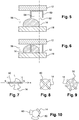
- each hollow and open insert 50 of the first component 12 is placed in line with a solid connection element 14 of the second component 16, by a solder ball, so that a portion 52 of the opening 54 of the insert 50 is not facing the element 14 ( figure 5 ).
- the patterns formed by the inserts 50 on the face of the component 12 are offset with respect to the pattern formed by the elements 14 on the face of the component 16.
- This offset of the patterns is for example obtained during the manufacture of the components. 12 and 16 followed by the implementation of a conventional alignment of the components, or the manufacture of the inserts 50 and elements 14 is performed in a conventional manner and the components 12 and 16 are then shifted during insertion.
- the invention makes it possible in particular to use the conventional patterns of the state of the art, the offset of which ensures the creation of the leakage passages for the gases.
- the portion 52 is for example of the order of 1 to 2 microns, even though the solid connection elements 14 are substantially distributed every 50 microns.
- the dimensions and shapes of the inserts are designed to create said passages.
- FIGS 7 to 10 are top views of preferred shapes of inserts and elements 14.
- the insert 50 takes the form of a hollow open bar whose length L along an x axis is greater than the length of the solid element 14 along said axis. Element 14 can take any form. The insert 50 thus exceeds each side of the element 50, thereby creating two passages for the gases.
- insert 50 has several branches, and takes the form for example of a cross ( figure 8 ) or a star ( figure 9 ), the ends of each branch protruding from the element 14.
- Each branch thus defines a passage for the gases.
- the solid element 14 may take any shape but is advantageously a spherical or ellipsoidal shape.
- the insert 50 is cylindrical and the solid element has lobes 60, the insert 50 being centered, not necessarily precisely, where the lobes 60 meet.
- the hollow insert is advantageously made of a hard material, such as in particular W, WSi, TiN, Cu, Pt or Ni, covered by a layer of noble metal, such as in particular Au or Pt in order to avoid surface oxide formation which would weaken the electrical contact with the solid element.
- the solid element is preferably constituted by In or an In-based composite, such as InSb, an alloy based on tin, lead, Al or an Al alloy, such as for example AlCu.
- the hollow insert is of tubular shape, its section being a hollow disk, the thickness e of walls, for example consisting of a film, is equal to 0.2 micrometer and whose diameter External D is 3.6 micrometers.
- the relation S ' ⁇ S / 2 is satisfied, as well as the relation e ⁇ D / 5.
- the insertion of hollow inserts into solid elements is used to make an assembly by the so-called " flip chip” technique in which a plurality of connections is formed between a first and a second electronic component.
- the connections are usually arranged in the form of a matrix of connections whose connections are spaced by a constant pitch p .
- the dimensions of the tubular hollow inserts are defined with respect to the pitch p of the connection matrix. More particularly, the height Ht of the insert is equal to p / 4, the external diameter D of the tubular hollow insert is equal to p / 2.5, and the thickness e of the walls of the hollow insert is equal to at D / 20 if p ⁇ 10 ⁇ m.
- the solid elements are in turn of elliptical section, whose major axis Dmax is at least 10% greater than the outer diameter D of the hollow inserts and whose minor axis is at least 10% smaller than the diameter D to create the gas outlet passages.
Description
L'invention a trait au domaine de la microélectronique, et plus particulièrement à l'assemblage de deux composants électroniques selon la technique dite de « flip chip » par thermo-compression.The invention relates to the field of microelectronics, and more particularly to the assembly of two electronic components according to the so-called " flip chip" technique by thermo-compression.
L'invention s'applique avantageusement aux dispositifs requérant des interconnexions de motifs métalliques à très petits pas, notamment pour la fabrication d'imageurs de très grandes dimensions et à très petits pas, comme par exemple les matrices de détection hétérogènes de grande taille comprenant un grand nombre de connexions, des matrices de détection sensibles à la température et hybridées à froid, ou encore des matrices de détection sensibles aux contraintes mécaniques.The invention is advantageously applicable to devices requiring interconnections of metal units with very small steps, in particular for the production of imagers of very large dimensions and with very small steps, such as, for example, large heterogeneous detection matrices comprising a a large number of connections, temperature-sensitive and cold-hybridized detection matrices, or detection matrices sensitive to mechanical stresses.
L'assemblage par la technique dite de « flip chip » par thermocompression consiste usuellement à former des billes électriquement conductrices sur une face d'un premier composant électronique et sur une face d'un second composant selon un motif de connexion prédéterminé. Le premier composant est alors reporté sur le second composant de manière à mettre en correspondance les billes respectives de soudure de ceux-ci puis l'ensemble est pressé et chauffé. Les billes mises en contact se déforment et fondent pour former des connexions électriques perpendiculaires au plan principal des composants électroniques, généralement sous la forme d'une tranche.The assembly by the so-called " flip chip" technique by thermocompression usually consists of forming electrically conductive balls on a face of a first electronic component and on a face of a second component according to a predetermined connection pattern. The first component is then transferred to the second component so as to match the respective solder balls thereof and the assembly is pressed and heated. The contacted beads deform and melt to form electrical connections perpendicular to the main plane of the electronic components, usually in the form of a wafer.
La miniaturisation des dispositifs électroniques a par ailleurs mené à une multiplication des connexions électriques requises par unité de surface. Ce faisant la compression d'un premier composant sur un second composant selon cette technique a nécessité une pression de compression toujours plus grande et donc une perte de contrôle de l'écrasement des billes.The miniaturization of electronic devices has also led to a multiplication of electrical connections required per unit area. In doing so the compression of a first component on a second component according to this technique required an ever greater compression pressure and therefore a loss of control of the crushing of the balls.
Pour pallier cette difficulté, les billes ménagées sur la face de l'un des composant ont été remplacées par une protubérance de section réduite en matériau plus dure que celui constitutif des billes. Lors de compression des composants, ces protubérances cassent l'oxyde natif des billes de l'autre composant, et cela même à basse température, grâce à une section d'appui plus faible. Une réduction de la pression exercée, ou un nombre de connexions par unité de surface plus grande pour une même pression, est ainsi obtenue. Conjointement, la compression nécessite une température plus basse et un meilleur contrôle de l'écrasement des billes est obtenu. On peut par exemple se référer au document
Quand bien même un gain appréciable au niveau de la pression soit obtenu par rapport à la première technique de « flip-chip », il n'en demeure pas moins que la pression nécessaire augmente à mesure que le nombre de connexions par unité de surface augmente. De fait, cette technique de « flip-chip » par insertion de protubérances dures dans des billes connaît in fine les mêmes limitations.Even if an appreciable gain in pressure is obtained compared to the first technique of "flip-chip", the fact remains that the necessary pressure increases as the number of connections per unit area increases . In fact, this technique of "flip-chip" by inserting hard protuberances in balls knows in fine the same limitations.
Afin de réduire encore la pression nécessaire lors de la thermocompression, les protubérances, qui forment des éléments pleins, ont été remplacés par des inserts creux et ouverts. Ainsi la surface d'appui des inserts sur les billes se limite à la surface de l'ouverture. On peut avantageusement se reporter à la demande
Les
Sur la
Une fois l'ouverture 20 de l'insert 10 introduite dans la bille 14, il n'existe plus de passage par lequel le gaz compris dans l'insert 10 puisse s'échapper. Une fois l'insertion terminée (
Pour pallier ce problème de bulle de gaz compressé, il a été conçu des inserts cylindriques biseautés, comme cela est illustré aux
Si le problème de la bulle de gaz compressé est ainsi résolu, cette technique nécessite l'utilisation d'un insert biseauté, dont la fabrication est plus complexe qu'un insert non biseauté, ainsi que la mise en oeuvre de deux étapes distinctes (pré-insertion et insertion sous vide) réduisant le rendement de fabrication de l'ensemble. En outre, cette technique nécessite l'utilisation d'une pompe à vide supplémentaire.If the problem of the compressed gas bubble is thus solved, this technique requires the use of a beveled insert, the manufacture of which is more complex than a non-beveled insert, as well as the implementation of two distinct steps ( vacuum insertion and insertion) reducing the manufacturing efficiency of the assembly. In addition, this technique requires the use of an additional vacuum pump.
Le but de la présente invention est de proposer un procédé d'assemblage de deux composants électroniques par insertion d'inserts creux et ouverts dans des éléments pleins, permettant une insertion sous atmosphère ambiante et sans création de bulle.The object of the present invention is to provide a method of assembling two electronic components by inserting hollow and open inserts in solid elements, allowing insertion in ambient atmosphere and without creating bubbles.
A cet effet, l'invention se caractérise par le fait que, lors de l'insertion d'un insert dans un élément plein convexe, au moins une surface de l'extrémité ouverte de l'insert est laissée libre de manière à créer un passage de sortie pour des gaz contenus dans l'insert.For this purpose, the invention is characterized in that, during the insertion of an insert into a convex solid element, at least one surface of the open end of the insert is left free so as to create an outlet passage for gases contained in the insert.
Par « insert creux », on entend ici un motif protubérant à partir d'une surface, dont les parois latérales forment une cavité interne ouverte, et dont l'épaisseur e des parois est faible par rapport aux dimensions de l'ouverture de la cavité, de manière à définir une surface d'appui réduite lors de l'étape d'insertion de l'insert creux dans l'élément plein, et donc une force d'insertion réduite par rapport à l'insertion d'un insert plein dans un élément plein, permettant ainsi l'insertion de l'insert dans l'élément plein sous atmosphère ambiante, sans étape de thermocompression ou de refusion.By "hollow insert" is meant here a protruding pattern from a surface, whose side walls form an open internal cavity, and whose wall thickness e is small compared to the dimensions of the opening of the cavity , so as to define a reduced bearing surface during the step of insertion of the hollow insert into the solid element, and therefore a reduced insertion force compared to the insertion of a solid insert into a solid element, thus allowing insertion of the insert into the solid element under ambient atmosphere, without thermocompression or reflow step.
A titre d'exemple numérique, la surface S' définie par les parois de l'insert creux est inférieure d'au moins de moitié à la surface S de la section de l'insert creux ( S'< S /2). Par exemple, dans le cas d'un insert creux tubulaire, l'épaisseur e des parois est inférieure au cinquième du diamètre externe D de l'insert ( e<D /5). On se reportera à la demande
De manière privilégiée, l'insert creux est formé par un film mince refermé sur lui-même dont la section est faible par rapport à la section de l'ouverture.In a preferred manner, the hollow insert is formed by a thin film closed on itself whose section is small relative to the section of the opening.
En d'autres termes, une portion de l'ouverture de l'insert est latéralement décalée de l'élément plein de sorte que cette portion n'est jamais insérée dans celui-ci. Il existe ainsi un passage pour les gaz lorsque ceux-ci sont chassés de l'insert par l'élément plein lors de l'insertion.In other words, a portion of the opening of the insert is laterally offset from the solid member so that this portion is never inserted therein. There is thus a passage for the gases when they are driven from the insert by the solid element during insertion.
Selon l'invention, les éléments pleins forment un motif sur une surface de l'un des composants, les inserts forment un motif sur une surface de l'autre composant et l'insertion est mise en oeuvre en décalant un motif par rapport à l'autre de manière à créer un passage de sortie des gaz pour chaque insert.According to the invention, the solid elements form a pattern on one surface of one of the components, the inserts form a pattern on one surface of the other component and the insertion is implemented by shifting a pattern relative to the other. other so as to create a gas outlet passage for each insert.
Selon des modes de réalisation particuliers de l'invention, le procédé comprend une ou plusieurs des caractéristiques suivantes, comme défini par les revendications annexées:
- ▪ l'extrémité ouverte de l'insert a une longueur, selon au moins un axe prédéterminé, supérieure à la longueur de l'élément plein selon ledit au moins un axe ;
- ▪ l'insert présente plusieurs branches prenant la forme d'une croix ou d'une étoile, les extrémités de chaque branche dépassant de l'élément plein lors de l'insertion;
- ▪ l'extrémité ouverte de l'insert est circulaire ;
- ▪ the open end of the insert has a length, along at least one predetermined axis, greater than the length of the solid element along said at least one axis;
- ▪ the insert has several branches in the form of a cross or a star, the ends of each branch protruding from the solid element during insertion;
- ▪ the open end of the insert is circular;
La présente invention sera mieux comprise à la lecture de la description qui va suivre, donnée uniquement à titre d'exemple, et faite en relation avec les dessins annexés, dans lesquels des références identiques désignent des éléments identiques ou analogues, et dans lesquels :
- ▪ les
figures 1 et 2 sont des vues en section illustrant l'insertion d'un insert creux et ouverts dans une bille selon un première technique de l'état antérieur de la technique, ces figures ayant été décrites dans le préambule ; - ▪ les
figures 3 et 4 sont des vues en section illustrant l'insertion d'un insert creux et ouverts dans une bille selon un deuxième technique de l'état antérieur de la technique, ces figures ayant été décrites dans le préambule ; - ▪ les
figures 5 et 6 sont des vues en section illustrant l'insertion d'un insert creux et ouverts dans une bille selon l'invention ; - ▪ les
figures 7 à 10 illustrent des formes privilégiées d'inserts selon l'invention.
- ▪ the
Figures 1 and 2 are sectional views illustrating the insertion of a hollow insert and open in a ball according to a first technique of the prior art, these figures having been described in the preamble; - ▪ the
Figures 3 and 4 are sectional views illustrating the insertion of a hollow insert and open in a ball according to a second technique of the prior art, these figures having been described in the preamble; - ▪ the
Figures 5 and 6 are sectional views illustrating the insertion of a hollow and open insert into a ball according to the invention; - ▪ the
Figures 7 to 10 illustrate preferred forms of inserts according to the invention.
En se référant aux
De fait, lors de l'insertion de l'insert 50 dans l'élément 14 selon la flèche 56 (
Selon l'invention, les motifs que forment les inserts 50 sur la face du composant 12 sont décalés par rapport au motif que forment les éléments 14 sur la face du composant 16. Ce décalage des motifs est par exemple obtenu lors de la fabrication des composants 12 et 16 suivi de la mise en oeuvre d'un alignement classique des composants, ou bien la fabrication des inserts 50 et des éléments 14 est réalisée de manière classique et les composants 12 et 16 sont ensuite décalés lors de l'insertion.According to the invention, the patterns formed by the
L'invention permet notamment d'utiliser les motifs classiques de l'état de la technique, le décalage de ceux-ci assurant la création des passages de fuite pour les gaz. Ainsi, la portion 52 est par exemple de l'ordre de 1 à 2 µm, alors même que les éléments pleins de connexion 14 sont sensiblement répartis tous les 50 µm.The invention makes it possible in particular to use the conventional patterns of the state of the art, the offset of which ensures the creation of the leakage passages for the gases. Thus, the
Dans un mode de réalisation particulier de l'invention, les dimensions et les formes des inserts sont conçues pour créer lesdits passages.In a particular embodiment of the invention, the dimensions and shapes of the inserts are designed to create said passages.
Les
Dans une première forme privilégiée illustrée à la
Dans une deuxième forme privilégiée illustrée aux
Dans une troisième forme privilégiée illustrée à la
Bien entendu d'autres modes de réalisation, tant en formes qu'en dimensions, sont possibles dès lors qu'au moins un passage pour les gaz est présent lors de l'insertion de l'insert dans l'élément plein.Of course other embodiments, both in shape and size, are possible since at least one passage for gases is present during insertion of the insert into the solid element.
L'insert creux est avantageusement constitué d'un matériau dur, tel que notamment du W, du WSi, du TiN, du Cu, du Pt ou du Ni, recouvert par une couche de métal noble, tel que notamment du Au ou du Pt, afin d'éviter la formation d'oxyde en surface qui affaiblirait le contact électrique avec l'élément plein. L'élément plein est quant à lui de préférence constitué d'In ou d'un composite à base d'In, comme par exemple du InSb, d'un alliage à base d'étain, de plomb, d'Al ou d'un alliage d'Al, comme par exemple du AlCu.The hollow insert is advantageously made of a hard material, such as in particular W, WSi, TiN, Cu, Pt or Ni, covered by a layer of noble metal, such as in particular Au or Pt in order to avoid surface oxide formation which would weaken the electrical contact with the solid element. The solid element is preferably constituted by In or an In-based composite, such as InSb, an alloy based on tin, lead, Al or an Al alloy, such as for example AlCu.
A titre d'exemple numérique, l'insert creux est de forme tubulaire, sa section étant un disque creux, dont l'épaisseur e des parois, par exemple constituées d'un film, est égale à 0,2 micromètre et dont le diamètre externe D est de 3,6 micromètres. Dans un tel cas, la relation S'< S/2 est remplie, ainsi que la relation e<D /5. As a numerical example, the hollow insert is of tubular shape, its section being a hollow disk, the thickness e of walls, for example consisting of a film, is equal to 0.2 micrometer and whose diameter External D is 3.6 micrometers. In such a case, the relation S '< S / 2 is satisfied, as well as the relation e < D / 5.
Comme dit plus haut, l'insertion d'inserts creux dans des éléments pleins est utilisée pour réaliser un assemblage par la technique dite de « flip chip » dans laquelle une pluralité de connexions est formée entre un premier et un second composants électroniques. Comme cela est connu en soit, les connexions sont usuellement agencées sous la forme d'une matrice de connexions dont les connexions sont espacées d'un pas p constant.As mentioned above, the insertion of hollow inserts into solid elements is used to make an assembly by the so-called " flip chip " technique in which a plurality of connections is formed between a first and a second electronic component. As is known in itself, the connections are usually arranged in the form of a matrix of connections whose connections are spaced by a constant pitch p .
De manière privilégiée, les dimensions des inserts creux tubulaires sont définies par rapport au pas p de la matrice de connexions. Plus particulièrement, la hauteur Ht de l'insert est égale à p /4, le diamètre externe D de l'insert creux tubulaire est égal à p /2,5, et l'épaisseur e des parois de l'insert creux est égale à D /20 si p ≤ 10µm.In a preferred manner, the dimensions of the tubular hollow inserts are defined with respect to the pitch p of the connection matrix. More particularly, the height Ht of the insert is equal to p / 4, the external diameter D of the tubular hollow insert is equal to p / 2.5, and the thickness e of the walls of the hollow insert is equal to at D / 20 if p ≤ 10μm.
Les éléments pleins sont quant à eux de section elliptique, dont le grand axe Dmax est supérieur d'au moins 10% au diamètre externe D des inserts creux et dont le petit axe est inférieur d'au moins 10% au diamètre D afin de créer les passages de sortie des gaz.The solid elements are in turn of elliptical section, whose major axis Dmax is at least 10% greater than the outer diameter D of the hollow inserts and whose minor axis is at least 10% smaller than the diameter D to create the gas outlet passages.
Ainsi les valeurs numériques récapitulées dans le tableau suivant sont obtenues.
Claims (4)
- A method for bonding two electronic components (12, 16) by the insertion of hollow and open inserts (50) into full convex elements (14) of lower hardness than that of the inserts, each hollow and open insert (50) having side walls forming an internal open cavity, the thickness of which being small relative to the dimensions of the cavity aperture, so as to define a small seat during the step of inserting the hollow and open insert (50) into the full convex element (14), and therefore a small insertion force relative to the insertion of a full insert into a full element, the inserts being configured for allowing the insertion of inserts (50) in full elements (14) under ambient atmosphere with no thermo-compression or re-fusion step, method in which, when an insert (50) is inserted into a full element (14), at least one surface (52) of the open end (54) of the insert (50) is left free so as to create an outlet passage for gases contained in the insert (50), characterized :▪ in that the full elements form a pattern on one surface of one of the components,▪ in that the inserts form a pattern on one surface of the other of the components, and▪ in that the insertion is performed by offsetting one pattern relative to the other so as to create an outlet passage for the gases in respect of each insert.
- The method for bonding two electronic components (12, 16) as claimed in claim 1, characterized in that the open end of the insert is of greater length, along at least one predetermined axis, than the length of the full element along said at least one axis.
- The method for bonding two electronic components (12, 16) as claimed in claim 2, characterized in that the insert has a plurality of branches assuming the shape of a cross or of a star, the end of each branch partially arranged outside the full element during the insertion.
- The method for bonding two electronic components (12, 16) as claimed in claim 2, characterized in that the open end of the insert is circular.
Applications Claiming Priority (1)
| Application Number | Priority Date | Filing Date | Title |
|---|---|---|---|
| FR0955657A FR2949171B1 (en) | 2009-08-13 | 2009-08-13 | METHOD FOR ASSEMBLING TWO ELECTRONIC COMPONENTS |
Publications (2)
| Publication Number | Publication Date |
|---|---|
| EP2287904A1 EP2287904A1 (en) | 2011-02-23 |
| EP2287904B1 true EP2287904B1 (en) | 2019-02-27 |
Family
ID=42040468
Family Applications (1)
| Application Number | Title | Priority Date | Filing Date |
|---|---|---|---|
| EP10305877.2A Active EP2287904B1 (en) | 2009-08-13 | 2010-08-10 | Method for assembling two electronic components |
Country Status (4)
| Country | Link |
|---|---|
| US (1) | US8291586B2 (en) |
| EP (1) | EP2287904B1 (en) |
| JP (1) | JP2011040754A (en) |
| FR (1) | FR2949171B1 (en) |
Families Citing this family (9)
| Publication number | Priority date | Publication date | Assignee | Title |
|---|---|---|---|---|
| CN105938825B (en) | 2011-05-24 | 2019-04-05 | 索尼公司 | Semiconductor image reception device |
| FR2981795B1 (en) | 2011-10-25 | 2015-01-02 | Commissariat Energie Atomique | FLIP-CHIP HYBRIDIZATION OF MICROELECTRONIC COMPONENTS BY LOCAL HEATING OF CONNECTION ELEMENTS |
| FR2994331B1 (en) | 2012-07-31 | 2014-09-12 | Commissariat Energie Atomique | METHOD FOR ASSEMBLING TWO ELECTRONIC COMPONENTS BETWEEN THEM, OF THE FLIP-CHIP TYPE |
| FR2996053A1 (en) * | 2012-09-27 | 2014-03-28 | Commissariat Energie Atomique | METHOD OF ASSEMBLING TWO ELECTRONIC COMPONENTS, OF THE FLIP-CHIP TYPE, ASSEMBLY OBTAINED ACCORDING TO THE METHOD |
| FR3003688B1 (en) * | 2013-03-22 | 2016-07-01 | Commissariat Energie Atomique | FLIP CHIP ASSEMBLY METHOD COMPRISING THE PRE-COATING OF INTERCONNECTING ELEMENTS |
| FR3018628A1 (en) | 2014-03-11 | 2015-09-18 | Commissariat Energie Atomique | METHOD FOR BONDING HYBRIDIZATION OF TWO MICROELECTRONIC ELEMENTS |
| JP6350759B2 (en) * | 2015-08-18 | 2018-07-04 | 三菱電機株式会社 | Semiconductor device |
| US10763249B2 (en) | 2018-05-31 | 2020-09-01 | Sharp Kabushiki Kaisha | Image display device |
| FR3119047A1 (en) * | 2021-01-21 | 2022-07-22 | Commissariat A L'energie Atomique Et Aux Energies Alternatives | SILICON ARMATURE MICRO-INSERT STRUCTURE |
Family Cites Families (10)
| Publication number | Priority date | Publication date | Assignee | Title |
|---|---|---|---|---|
| US5329423A (en) * | 1993-04-13 | 1994-07-12 | Scholz Kenneth D | Compressive bump-and-socket interconnection scheme for integrated circuits |
| US5767580A (en) * | 1993-04-30 | 1998-06-16 | Lsi Logic Corporation | Systems having shaped, self-aligning micro-bump structures |
| US6007349A (en) * | 1996-01-04 | 1999-12-28 | Tessera, Inc. | Flexible contact post and post socket and associated methods therefor |
| US6130148A (en) * | 1997-12-12 | 2000-10-10 | Farnworth; Warren M. | Interconnect for semiconductor components and method of fabrication |
| FR2876243B1 (en) | 2004-10-04 | 2007-01-26 | Commissariat Energie Atomique | DUCTILE BURST CONDUCTIVE PROTUBERANCE COMPONENT AND METHOD FOR ELECTRICAL CONNECTION BETWEEN THIS COMPONENT AND A COMPONENT HAVING HARD CONDUCTIVE POINTS |
| JP4636850B2 (en) * | 2004-10-29 | 2011-02-23 | 富士通株式会社 | Electronic component mounting method |
| US7456493B2 (en) * | 2005-04-15 | 2008-11-25 | Alps Electric Co., Ltd. | Structure for mounting semiconductor part in which bump and land portion are hardly detached from each other and method of manufacturing mounting substrate used therein |
| US7157372B1 (en) * | 2005-06-14 | 2007-01-02 | Cubic Wafer Inc. | Coaxial through chip connection |
| US7135771B1 (en) * | 2005-06-23 | 2006-11-14 | Intel Corporation | Self alignment features for an electronic assembly |
| FR2928033B1 (en) | 2008-02-22 | 2010-07-30 | Commissariat Energie Atomique | CONNECTING COMPONENT HAVING HOLLOW INSERTS. |
-
2009
- 2009-08-13 FR FR0955657A patent/FR2949171B1/en not_active Expired - Fee Related
-
2010
- 2010-08-09 US US12/852,726 patent/US8291586B2/en active Active
- 2010-08-10 EP EP10305877.2A patent/EP2287904B1/en active Active
- 2010-08-12 JP JP2010180904A patent/JP2011040754A/en not_active Withdrawn
Non-Patent Citations (1)
| Title |
|---|
| None * |
Also Published As
| Publication number | Publication date |
|---|---|
| FR2949171A1 (en) | 2011-02-18 |
| FR2949171B1 (en) | 2011-08-26 |
| JP2011040754A (en) | 2011-02-24 |
| US8291586B2 (en) | 2012-10-23 |
| US20110035925A1 (en) | 2011-02-17 |
| EP2287904A1 (en) | 2011-02-23 |
Similar Documents
| Publication | Publication Date | Title |
|---|---|---|
| EP2287904B1 (en) | Method for assembling two electronic components | |
| EP2175485B1 (en) | Connection between two plugged and soldered inserts and method of manufacturing the same | |
| EP2250667B1 (en) | Assembly including a wire member and a microelectronic chip with a notch, including at least one stud for holding the wire member | |
| EP2339618B1 (en) | Method for assembling at least one chip with a wired element, electronic chip with deformable connection element, method for manufacturing a plurality of chips and assembly of at least one chip with a wired element | |
| EP2618368A1 (en) | Connection component with hollow inserts and method of making the same | |
| EP2738796A2 (en) | Method for producing a flip-chip structure for assembling microelectronic devices comprising an insulating block for guiding a connecting element and corresponding device | |
| EP2976784A1 (en) | Flip-chip assembly process comprising pre-coating interconnect elements | |
| FR2980036A1 (en) | Method for realizing three-dimensional integrated structure, involves realizing electrically conductive through-connection extending between non-assembled face and metal line of interconnection part of one of two integrated circuits | |
| EP3501042A1 (en) | Method for connecting cross-components at optimised density | |
| EP3035017B1 (en) | Differential temperature sensor | |
| EP2636064B1 (en) | Connecting elements for producing hybrid electronic circuits | |
| EP2693468A1 (en) | Method for flip-chip assembly of two electronic components | |
| EP3031775B1 (en) | Method for producing an electrical connection in a blind via | |
| EP1147557A1 (en) | Integrated circuit device, electronic module for chip card using said device and method for making same | |
| FR3127644A1 (en) | Connector | |
| EP2519087B1 (en) | Cover for encapsulating a system with electrical connections, manufacturing process therefore, encapsulated system comprising such a cover and piling of such systems | |
| EP0985334A1 (en) | Electronic component adapter | |
| WO2012120245A1 (en) | Connection component provided with hollow inserts | |
| EP2205053A1 (en) | Printed circuit card and process for producing such a card | |
| FR2978869A1 (en) | Method for assembling integrated circuits for forming integrated three-dimensional structure, involves fusing alloy layer at low melting point to form conducting connection between metal lines of two integrated circuits | |
| FR2969374A1 (en) | METHOD FOR ASSEMBLING TWO INTEGRATED CIRCUITS AND CORRESPONDING STRUCTURE | |
| WO2005018090A1 (en) | Microsystem incorporating at least one resonant structure in a cavity under a controlled atmosphere, and method for producing the same | |
| FR2978610A1 (en) | Method for making electrically conductive connection in semiconductor substrate of three-dimensional integrated structure, involves thinning substrate from face of substrate up to pillar that is guided on another face of substrate | |
| WO2010081967A1 (en) | Method of fabricating an electronic module, especially for electronic chip-based identification device |
Legal Events
| Date | Code | Title | Description |
|---|---|---|---|
| PUAI | Public reference made under article 153(3) epc to a published international application that has entered the european phase |
Free format text: ORIGINAL CODE: 0009012 |
|
| AK | Designated contracting states |
Kind code of ref document: A1 Designated state(s): AL AT BE BG CH CY CZ DE DK EE ES FI FR GB GR HR HU IE IS IT LI LT LU LV MC MK MT NL NO PL PT RO SE SI SK SM TR |
|
| AX | Request for extension of the european patent |
Extension state: BA ME RS |
|
| 17P | Request for examination filed |
Effective date: 20110120 |
|
| RAP1 | Party data changed (applicant data changed or rights of an application transferred) |
Owner name: COMMISSARIAT A L'ENERGIE ATOMIQUE ET AUX ENERGIES |
|
| RIN1 | Information on inventor provided before grant (corrected) |
Inventor name: MARION, FRANCOIS |
|
| STAA | Information on the status of an ep patent application or granted ep patent |
Free format text: STATUS: EXAMINATION IS IN PROGRESS |
|
| 17Q | First examination report despatched |
Effective date: 20170508 |
|
| RIC1 | Information provided on ipc code assigned before grant |
Ipc: H01L 23/485 20060101AFI20181025BHEP Ipc: H01L 21/98 20060101ALI20181025BHEP Ipc: H01L 25/065 20060101ALI20181025BHEP Ipc: H01L 21/60 20060101ALI20181025BHEP |
|
| GRAP | Despatch of communication of intention to grant a patent |
Free format text: ORIGINAL CODE: EPIDOSNIGR1 |
|
| STAA | Information on the status of an ep patent application or granted ep patent |
Free format text: STATUS: GRANT OF PATENT IS INTENDED |
|
| INTG | Intention to grant announced |
Effective date: 20181205 |
|
| GRAS | Grant fee paid |
Free format text: ORIGINAL CODE: EPIDOSNIGR3 |
|
| GRAA | (expected) grant |
Free format text: ORIGINAL CODE: 0009210 |
|
| STAA | Information on the status of an ep patent application or granted ep patent |
Free format text: STATUS: THE PATENT HAS BEEN GRANTED |
|
| AK | Designated contracting states |
Kind code of ref document: B1 Designated state(s): AL AT BE BG CH CY CZ DE DK EE ES FI FR GB GR HR HU IE IS IT LI LT LU LV MC MK MT NL NO PL PT RO SE SI SK SM TR |
|
| REG | Reference to a national code |
Ref country code: GB Ref legal event code: FG4D Free format text: NOT ENGLISH |
|
| REG | Reference to a national code |
Ref country code: CH Ref legal event code: EP |
|
| REG | Reference to a national code |
Ref country code: AT Ref legal event code: REF Ref document number: 1102565 Country of ref document: AT Kind code of ref document: T Effective date: 20190315 |
|
| REG | Reference to a national code |
Ref country code: IE Ref legal event code: FG4D Free format text: LANGUAGE OF EP DOCUMENT: FRENCH |
|
| REG | Reference to a national code |
Ref country code: DE Ref legal event code: R096 Ref document number: 602010057195 Country of ref document: DE |
|
| REG | Reference to a national code |
Ref country code: NL Ref legal event code: MP Effective date: 20190227 |
|
| REG | Reference to a national code |
Ref country code: LT Ref legal event code: MG4D |
|
| PG25 | Lapsed in a contracting state [announced via postgrant information from national office to epo] |
Ref country code: NO Free format text: LAPSE BECAUSE OF FAILURE TO SUBMIT A TRANSLATION OF THE DESCRIPTION OR TO PAY THE FEE WITHIN THE PRESCRIBED TIME-LIMIT Effective date: 20190527 Ref country code: FI Free format text: LAPSE BECAUSE OF FAILURE TO SUBMIT A TRANSLATION OF THE DESCRIPTION OR TO PAY THE FEE WITHIN THE PRESCRIBED TIME-LIMIT Effective date: 20190227 Ref country code: SE Free format text: LAPSE BECAUSE OF FAILURE TO SUBMIT A TRANSLATION OF THE DESCRIPTION OR TO PAY THE FEE WITHIN THE PRESCRIBED TIME-LIMIT Effective date: 20190227 Ref country code: NL Free format text: LAPSE BECAUSE OF FAILURE TO SUBMIT A TRANSLATION OF THE DESCRIPTION OR TO PAY THE FEE WITHIN THE PRESCRIBED TIME-LIMIT Effective date: 20190227 Ref country code: PT Free format text: LAPSE BECAUSE OF FAILURE TO SUBMIT A TRANSLATION OF THE DESCRIPTION OR TO PAY THE FEE WITHIN THE PRESCRIBED TIME-LIMIT Effective date: 20190627 Ref country code: LT Free format text: LAPSE BECAUSE OF FAILURE TO SUBMIT A TRANSLATION OF THE DESCRIPTION OR TO PAY THE FEE WITHIN THE PRESCRIBED TIME-LIMIT Effective date: 20190227 |
|
| PG25 | Lapsed in a contracting state [announced via postgrant information from national office to epo] |
Ref country code: HR Free format text: LAPSE BECAUSE OF FAILURE TO SUBMIT A TRANSLATION OF THE DESCRIPTION OR TO PAY THE FEE WITHIN THE PRESCRIBED TIME-LIMIT Effective date: 20190227 Ref country code: LV Free format text: LAPSE BECAUSE OF FAILURE TO SUBMIT A TRANSLATION OF THE DESCRIPTION OR TO PAY THE FEE WITHIN THE PRESCRIBED TIME-LIMIT Effective date: 20190227 Ref country code: GR Free format text: LAPSE BECAUSE OF FAILURE TO SUBMIT A TRANSLATION OF THE DESCRIPTION OR TO PAY THE FEE WITHIN THE PRESCRIBED TIME-LIMIT Effective date: 20190528 Ref country code: IS Free format text: LAPSE BECAUSE OF FAILURE TO SUBMIT A TRANSLATION OF THE DESCRIPTION OR TO PAY THE FEE WITHIN THE PRESCRIBED TIME-LIMIT Effective date: 20190627 Ref country code: BG Free format text: LAPSE BECAUSE OF FAILURE TO SUBMIT A TRANSLATION OF THE DESCRIPTION OR TO PAY THE FEE WITHIN THE PRESCRIBED TIME-LIMIT Effective date: 20190527 |
|
| REG | Reference to a national code |
Ref country code: AT Ref legal event code: MK05 Ref document number: 1102565 Country of ref document: AT Kind code of ref document: T Effective date: 20190227 |
|
| PG25 | Lapsed in a contracting state [announced via postgrant information from national office to epo] |
Ref country code: EE Free format text: LAPSE BECAUSE OF FAILURE TO SUBMIT A TRANSLATION OF THE DESCRIPTION OR TO PAY THE FEE WITHIN THE PRESCRIBED TIME-LIMIT Effective date: 20190227 Ref country code: DK Free format text: LAPSE BECAUSE OF FAILURE TO SUBMIT A TRANSLATION OF THE DESCRIPTION OR TO PAY THE FEE WITHIN THE PRESCRIBED TIME-LIMIT Effective date: 20190227 Ref country code: IT Free format text: LAPSE BECAUSE OF FAILURE TO SUBMIT A TRANSLATION OF THE DESCRIPTION OR TO PAY THE FEE WITHIN THE PRESCRIBED TIME-LIMIT Effective date: 20190227 Ref country code: RO Free format text: LAPSE BECAUSE OF FAILURE TO SUBMIT A TRANSLATION OF THE DESCRIPTION OR TO PAY THE FEE WITHIN THE PRESCRIBED TIME-LIMIT Effective date: 20190227 Ref country code: CZ Free format text: LAPSE BECAUSE OF FAILURE TO SUBMIT A TRANSLATION OF THE DESCRIPTION OR TO PAY THE FEE WITHIN THE PRESCRIBED TIME-LIMIT Effective date: 20190227 Ref country code: ES Free format text: LAPSE BECAUSE OF FAILURE TO SUBMIT A TRANSLATION OF THE DESCRIPTION OR TO PAY THE FEE WITHIN THE PRESCRIBED TIME-LIMIT Effective date: 20190227 Ref country code: SK Free format text: LAPSE BECAUSE OF FAILURE TO SUBMIT A TRANSLATION OF THE DESCRIPTION OR TO PAY THE FEE WITHIN THE PRESCRIBED TIME-LIMIT Effective date: 20190227 Ref country code: AL Free format text: LAPSE BECAUSE OF FAILURE TO SUBMIT A TRANSLATION OF THE DESCRIPTION OR TO PAY THE FEE WITHIN THE PRESCRIBED TIME-LIMIT Effective date: 20190227 |
|
| REG | Reference to a national code |
Ref country code: DE Ref legal event code: R097 Ref document number: 602010057195 Country of ref document: DE |
|
| PG25 | Lapsed in a contracting state [announced via postgrant information from national office to epo] |
Ref country code: PL Free format text: LAPSE BECAUSE OF FAILURE TO SUBMIT A TRANSLATION OF THE DESCRIPTION OR TO PAY THE FEE WITHIN THE PRESCRIBED TIME-LIMIT Effective date: 20190227 Ref country code: SM Free format text: LAPSE BECAUSE OF FAILURE TO SUBMIT A TRANSLATION OF THE DESCRIPTION OR TO PAY THE FEE WITHIN THE PRESCRIBED TIME-LIMIT Effective date: 20190227 |
|
| PG25 | Lapsed in a contracting state [announced via postgrant information from national office to epo] |
Ref country code: AT Free format text: LAPSE BECAUSE OF FAILURE TO SUBMIT A TRANSLATION OF THE DESCRIPTION OR TO PAY THE FEE WITHIN THE PRESCRIBED TIME-LIMIT Effective date: 20190227 |
|
| PLBE | No opposition filed within time limit |
Free format text: ORIGINAL CODE: 0009261 |
|
| STAA | Information on the status of an ep patent application or granted ep patent |
Free format text: STATUS: NO OPPOSITION FILED WITHIN TIME LIMIT |
|
| 26N | No opposition filed |
Effective date: 20191128 |
|
| PG25 | Lapsed in a contracting state [announced via postgrant information from national office to epo] |
Ref country code: SI Free format text: LAPSE BECAUSE OF FAILURE TO SUBMIT A TRANSLATION OF THE DESCRIPTION OR TO PAY THE FEE WITHIN THE PRESCRIBED TIME-LIMIT Effective date: 20190227 |
|
| PG25 | Lapsed in a contracting state [announced via postgrant information from national office to epo] |
Ref country code: TR Free format text: LAPSE BECAUSE OF FAILURE TO SUBMIT A TRANSLATION OF THE DESCRIPTION OR TO PAY THE FEE WITHIN THE PRESCRIBED TIME-LIMIT Effective date: 20190227 |
|
| PG25 | Lapsed in a contracting state [announced via postgrant information from national office to epo] |
Ref country code: LU Free format text: LAPSE BECAUSE OF NON-PAYMENT OF DUE FEES Effective date: 20190810 Ref country code: LI Free format text: LAPSE BECAUSE OF NON-PAYMENT OF DUE FEES Effective date: 20190831 Ref country code: MC Free format text: LAPSE BECAUSE OF FAILURE TO SUBMIT A TRANSLATION OF THE DESCRIPTION OR TO PAY THE FEE WITHIN THE PRESCRIBED TIME-LIMIT Effective date: 20190227 Ref country code: CH Free format text: LAPSE BECAUSE OF NON-PAYMENT OF DUE FEES Effective date: 20190831 |
|
| REG | Reference to a national code |
Ref country code: BE Ref legal event code: MM Effective date: 20190831 |
|
| PG25 | Lapsed in a contracting state [announced via postgrant information from national office to epo] |
Ref country code: IE Free format text: LAPSE BECAUSE OF NON-PAYMENT OF DUE FEES Effective date: 20190810 |
|
| PG25 | Lapsed in a contracting state [announced via postgrant information from national office to epo] |
Ref country code: BE Free format text: LAPSE BECAUSE OF NON-PAYMENT OF DUE FEES Effective date: 20190831 |
|
| PG25 | Lapsed in a contracting state [announced via postgrant information from national office to epo] |
Ref country code: CY Free format text: LAPSE BECAUSE OF FAILURE TO SUBMIT A TRANSLATION OF THE DESCRIPTION OR TO PAY THE FEE WITHIN THE PRESCRIBED TIME-LIMIT Effective date: 20190227 |
|
| PG25 | Lapsed in a contracting state [announced via postgrant information from national office to epo] |
Ref country code: MT Free format text: LAPSE BECAUSE OF FAILURE TO SUBMIT A TRANSLATION OF THE DESCRIPTION OR TO PAY THE FEE WITHIN THE PRESCRIBED TIME-LIMIT Effective date: 20190227 Ref country code: HU Free format text: LAPSE BECAUSE OF FAILURE TO SUBMIT A TRANSLATION OF THE DESCRIPTION OR TO PAY THE FEE WITHIN THE PRESCRIBED TIME-LIMIT; INVALID AB INITIO Effective date: 20100810 |
|
| PG25 | Lapsed in a contracting state [announced via postgrant information from national office to epo] |
Ref country code: MK Free format text: LAPSE BECAUSE OF FAILURE TO SUBMIT A TRANSLATION OF THE DESCRIPTION OR TO PAY THE FEE WITHIN THE PRESCRIBED TIME-LIMIT Effective date: 20190227 |
|
| PGFP | Annual fee paid to national office [announced via postgrant information from national office to epo] |
Ref country code: GB Payment date: 20220824 Year of fee payment: 13 Ref country code: DE Payment date: 20220822 Year of fee payment: 13 |
|
| PGFP | Annual fee paid to national office [announced via postgrant information from national office to epo] |
Ref country code: FR Payment date: 20220822 Year of fee payment: 13 |