EP2284998A2 - Surface acoustic wave filter device - Google Patents
Surface acoustic wave filter device Download PDFInfo
- Publication number
- EP2284998A2 EP2284998A2 EP10173569A EP10173569A EP2284998A2 EP 2284998 A2 EP2284998 A2 EP 2284998A2 EP 10173569 A EP10173569 A EP 10173569A EP 10173569 A EP10173569 A EP 10173569A EP 2284998 A2 EP2284998 A2 EP 2284998A2
- Authority
- EP
- European Patent Office
- Prior art keywords
- acoustic wave
- surface acoustic
- wave filter
- parallel arm
- electrode
- Prior art date
- Legal status (The legal status is an assumption and is not a legal conclusion. Google has not performed a legal analysis and makes no representation as to the accuracy of the status listed.)
- Withdrawn
Links
Images


Classifications
-
- H—ELECTRICITY
- H03—ELECTRONIC CIRCUITRY
- H03H—IMPEDANCE NETWORKS, e.g. RESONANT CIRCUITS; RESONATORS
- H03H9/00—Networks comprising electromechanical or electro-acoustic devices; Electromechanical resonators
- H03H9/02—Details
- H03H9/05—Holders; Supports
- H03H9/10—Mounting in enclosures
- H03H9/1064—Mounting in enclosures for surface acoustic wave [SAW] devices
- H03H9/1071—Mounting in enclosures for surface acoustic wave [SAW] devices the enclosure being defined by a frame built on a substrate and a cap, the frame having no mechanical contact with the SAW device
-
- H—ELECTRICITY
- H03—ELECTRONIC CIRCUITRY
- H03H—IMPEDANCE NETWORKS, e.g. RESONANT CIRCUITS; RESONATORS
- H03H9/00—Networks comprising electromechanical or electro-acoustic devices; Electromechanical resonators
- H03H9/02—Details
- H03H9/05—Holders; Supports
- H03H9/0538—Constructional combinations of supports or holders with electromechanical or other electronic elements
- H03H9/0547—Constructional combinations of supports or holders with electromechanical or other electronic elements consisting of a vertical arrangement
- H03H9/0557—Constructional combinations of supports or holders with electromechanical or other electronic elements consisting of a vertical arrangement the other elements being buried in the substrate
-
- H—ELECTRICITY
- H03—ELECTRONIC CIRCUITRY
- H03H—IMPEDANCE NETWORKS, e.g. RESONANT CIRCUITS; RESONATORS
- H03H9/00—Networks comprising electromechanical or electro-acoustic devices; Electromechanical resonators
- H03H9/02—Details
- H03H9/05—Holders; Supports
- H03H9/058—Holders; Supports for surface acoustic wave devices
- H03H9/059—Holders; Supports for surface acoustic wave devices consisting of mounting pads or bumps
-
- H—ELECTRICITY
- H03—ELECTRONIC CIRCUITRY
- H03H—IMPEDANCE NETWORKS, e.g. RESONANT CIRCUITS; RESONATORS
- H03H9/00—Networks comprising electromechanical or electro-acoustic devices; Electromechanical resonators
- H03H9/46—Filters
- H03H9/64—Filters using surface acoustic waves
- H03H9/6423—Means for obtaining a particular transfer characteristic
- H03H9/6433—Coupled resonator filters
- H03H9/6483—Ladder SAW filters
-
- H—ELECTRICITY
- H01—ELECTRIC ELEMENTS
- H01L—SEMICONDUCTOR DEVICES NOT COVERED BY CLASS H10
- H01L2224/00—Indexing scheme for arrangements for connecting or disconnecting semiconductor or solid-state bodies and methods related thereto as covered by H01L24/00
- H01L2224/01—Means for bonding being attached to, or being formed on, the surface to be connected, e.g. chip-to-package, die-attach, "first-level" interconnects; Manufacturing methods related thereto
- H01L2224/10—Bump connectors; Manufacturing methods related thereto
- H01L2224/15—Structure, shape, material or disposition of the bump connectors after the connecting process
- H01L2224/16—Structure, shape, material or disposition of the bump connectors after the connecting process of an individual bump connector
- H01L2224/161—Disposition
- H01L2224/16151—Disposition the bump connector connecting between a semiconductor or solid-state body and an item not being a semiconductor or solid-state body, e.g. chip-to-substrate, chip-to-passive
- H01L2224/16221—Disposition the bump connector connecting between a semiconductor or solid-state body and an item not being a semiconductor or solid-state body, e.g. chip-to-substrate, chip-to-passive the body and the item being stacked
- H01L2224/16225—Disposition the bump connector connecting between a semiconductor or solid-state body and an item not being a semiconductor or solid-state body, e.g. chip-to-substrate, chip-to-passive the body and the item being stacked the item being non-metallic, e.g. insulating substrate with or without metallisation
-
- H—ELECTRICITY
- H01—ELECTRIC ELEMENTS
- H01L—SEMICONDUCTOR DEVICES NOT COVERED BY CLASS H10
- H01L2924/00—Indexing scheme for arrangements or methods for connecting or disconnecting semiconductor or solid-state bodies as covered by H01L24/00
- H01L2924/15—Details of package parts other than the semiconductor or other solid state devices to be connected
- H01L2924/161—Cap
- H01L2924/1615—Shape
- H01L2924/16195—Flat cap [not enclosing an internal cavity]
Definitions
- the present invention relates to a surface acoustic wave filter, and particularly to a surface acoustic wave filter device having a ladder type circuit.
- a plurality of one terminal pair surface acoustic wave resonators are connected in series between input terminal and output terminal as series arm resonators, and define series arms.
- a plurality of one terminal pair surface acoustic wave resonators are connected in parallel between the series arms and ground as parallel arm resonators, and define parallel arms.
- the band-pass filter having the ladder type circuit has small insertion loss and wide pass band, and is widely used as a band-pass filter in a portable telephone
- Japanese Unexamined Patent Application Publication No. 05-183380 discloses that an inductance component is connected in series to the above-described series arm resonator or parallel arm resonator, and this allows the band-widening of filter characteristics.
- the Japanese Unexamined Patent Application Publication No. 10-93382 discloses a structure wherein an inductance is added to parallel arm resonators in a surface acoustic wave filter device having a ladder type circuit.
- Fig. 18 shows a circuit configuration of the surface acoustic wave filter device disclosed in this prior art.
- the surface acoustic wave filter device 501 series arm resonators S1 and S2 and parallel arm resonators P1 to P3 are connected to one another so as to constitute a ladder type circuit.
- an inductance L is inserted between the parallel arm resonators P1 to P3 and the ground potential, and thereby the widening of pass band and the increase in attenuation value in the vicinity of a pass band are achieved.
- Japanese Unexamined Patent Application Publication No. 04-65909 discloses a structure in which a surface acoustic wave filter element is connected to a package by means of the face down process.
- the electrodes of a package and those of the surface acoustic wave filter element has been connected by bonding wires.
- the surface acoustic wave filter device disclosed in this prior art has achieved a reduction in the size by adopting the face down process.
- Fig. 19 shows a schematic sectional view of a package of a surface acoustic wave filter element accommodated by using this face down process.
- a surface acoustic wave filter element 603 is accommodated in a package 602.
- the package 602 includes a base board 602a, a side wall 602b, and a cap 602c.
- the surface acoustic wave filter element 603 has a piezoelectric substrate 603a, and electrodes for constructing surface acoustic wave filter element are formed on the bottom surface of the piezoelectric substrate 603a.
- the electrodes formed on the bottom surface of the piezoelectric substrate 603a are electrically connected to the electrode pads in the die-attach portion 602d via bumps 604, and the surface acoustic wave filter element 603 is mechanically fixed to the die-attach portion 602d by the bumps 604.
- the surface acoustic wave filter device 601 which is packaged by above-described face down process, since no bonding wire is provided, an inductance component can not be added to the surface acoustic wave filter device 601 by the bonding wire. It is possible to obtain a small inductance component by rooting electrodes connecting the external electrodes provided on the package and the die-attach portion, but a large inductance can not be obtained by such rooting electrodes.
- the Japanese Unexamined Patent Application Publication No. 04-65909 describes that, by adding inductance components between each of the input/output signal terminals and the ground terminal in the package, an input/output impedance matching can be achieved without using external elements.
- This description is pertinent to a surface acoustic wave filter having a structure which must achieve an input/output impedance matching outside the surface acoustic wave filter. Accordingly, in the case of a surface acoustic wave filter having a ladder circuit configuration which intrinsically needs not be matched to be 50 ⁇ , it is unnecessary to achieve an impedance matching between each of the input/output signal terminals and the ground terminal in such a package.
- inductance components are formed in the die-attach portion, but with this structure, an electromagnetic coupling occurs between the wiring and the like and the die-attach portion on the piezoelectric substrate of the surface acoustic wave filter element, so that the filter characteristics thereof deteriorate.
- the position and the number of bumps do not necessarily achieve the sufficient electrical connections and mechanical bonding, reliability of surface acoustic wave filter device deteriorates.
- the object of the present invention is to overcome the above-described drawbacks of the prior art, and to provide a surface acoustic wave filter device with excellent filter characteristics, in which a surface acoustic wave filter element having a ladder type circuit is accommodated in a package by means of the face down process.
- Inductances are added to parallel arm resonators and/or series arm resonators, and the deterioration of filter characteristics by the electromagnetic coupling between the electrodes on the surface acoustic wave filter element and the inductances provided in the package hardly occurs.
- the limitations on the position and the number of bumps is low.
- a surface acoustic wave filter device comprising a surface acoustic wave filter element which includes a piezoelectric substrate and a plurality of one terminal pair surface acoustic wave elements formed on the piezoelectric substrate, and in which the one terminal pair surface acoustic wave elements are connected so as to define a parallel arm resonator and a series arm resonator in a ladder circuit; and a package accommodating the surface acoustic wave filter element.
- the surface acoustic wave filter element is bonded via a plurality of bumps by means of the face down process and is accommodated in the package.
- This surface acoustic wave filter device further comprises an inductance component of a microstrip line which is provided in said package and connected to at least one of the series arm resonator and the parallel arm resonator.
- the above-described package includes a die-attach portion including a plurality of electrode pads which are connected via the bumps to one of a signal terminal and a ground terminal of the surface acoustic wave filter element; and a plurality of external electrodes which are electrically connected to at least one of the electrode pads, and connected to one of a signal line and a ground line outside the surface acoustic wave filter device.
- the above described microstrip line is connected between the electrode pad connected to the signal terminal of the series arm resonator and the external electrode connected to the signal line outside the surface acoustic wave filter device.
- the above-described microstrip line is provided between the electrode pad connected to the ground terminal of at least one parallel arm resonator via the bumps, and the external electrode which is connected to the ground line outside the package.
- the surface acoustic wave filter device in accordance with the present invention comprises at least two parallel arm resonators.
- the ground terminals of all the parallel arm resonators are commonly connected on the piezoelectric substrate, and the microstrip line is connected between the portion where the ground terminals of the parallel arm resonators are commonly connected and the external electrode provided in the package.
- the surface acoustic wave filter device in accordance with the present invention comprises at least two parallel arm resonators.
- the package-side electrode pads connected to the ground terminals of all the parallel arm resonators are made a common electrode pad, and the microstrip line is provided on the path between the common electrode pad and the external electrode.
- the surface acoustic wave filter device in accordance with the present invention comprises at least three parallel arm resonators; and an electrode land which is provided on the piezoelectric substrate, and to which the ground terminals of at least two parallel arm resonators are each connected.
- the microstrip line is provided on the path between the electrode land connected to the ground terminals of at least two parallel arm resonators and the external electrode to which the electrode land is connected; and the parallel arm resonator other than the above-described at least two parallel arm resonators is electrically isolated from the above-described at least two parallel arm resonators on the piezoelectric substrate, and is electrically connected to the external electrode other than the package-side external electrode connected to the above-described at least two parallel arm resonators.
- the surface acoustic wave filter device in accordance with the present invention comprises at least three parallel arm resonators.
- the plurality of electrode pads include a common electrode pad connected to the ground terminals of at least two parallel arm resonators among the parallel arm resonators, and the microstrip line is provided on the path between the common electrode pad and the external electrode to which the common electrode pad is connected; and the parallel arm resonator other than the above-described at least two parallel arm resonators is electrically isolated from the above-described at least two parallel arm resonators, at a die-attach portion including the plurality of electrode pads, and is electrically connected to the external electrode other than the package-side external electrode connected to the above-described at least two parallel arm resonators.
- the above-described microstrip line is disposed in the package at the position other than the position of the die-attach portion.
- the above-described package comprises a base board on which the surface acoustic wave filter element is mounted; an annular side wall provided on the base board; and a cap member attached to the annual side wall so as to close the upper end thereof.
- a main portion of the microstrip line is disposed between the side wall and the base board.
- the above-described package comprises a first case member on which the surface acoustic wave filter element is mounted; and a second case member enclosing the surface acoustic wave filter element mounted on the first case member.
- a main portion of the microstrip line is provided inside the first case member.
- a main portion of a microstrip line refers to at least 50% of the entire length of a microstrip line.
- the signal terminal at the input/output end of the surface acoustic wave filter element and at least one ground terminal thereof are arranged so as to be rotated by 90° about the imaginary line which passes the center of the piezoelectric substrate of the surface acoustic wave filter element, and which is perpendicular to the piezoelectric substrate, with respect to the external electrode connected to the signal line at the input/output end and the external electrode connected to at least one ground potential among the plurality of external electrodes.
- the communication device in accordance with the present invention is characterized by comprising a surface acoustic wave filter device in accordance with the present invention.
- the surface acoustic wave filter device 1 in accordance with the present embodiment includes a package 2, and a surface acoustic wave filter element 3 accommodated in a package 2.
- Fig. 1 only schematically shows an appearance of the surface acoustic wave filter device 3.
- the package 2 comprises a base board 4 having a rectangular plate shape, a rectangular frame-shaped side wall 5 bonded on the base board 4, and a rectangular plate-shaped cap member 6 affixed to the side wall 5 so as to close the upper opening thereof.
- the side wall 5 does not necessarily requires to be rectangular, but may have a ringshaped structure such as annular shape.
- the base board 4 and the side wall 5 may be made of an insulative ceramic such as alumina, or a synthetic resin.
- the cap member 6 may also be made of a similar material.
- the cap member 6 may be made of a metal or the like in order to have an electromagnetic shielding property.
- the base board 4 is constructed by a multilayer substrate including substrates 4b and 4c. Between the substrate 4a and the substrate 4b, a ground electrode 50 for microstrip line which is described later is provided on a substantially entire surface of the substrate 4b.
- the substrates 4b and 4c are made of insulative material and have a predetermined dielectric constant.
- the surface acoustic wave filter element 3 has a rectangular plate-shaped piezoelectric substrate 7 as a piezoelectric substrate.
- the piezoelectric substrate 7 is made of a 36°, Y-cut, and X-propagation LiTaO 3 substrate.
- the piezoelectric substrate 7, however, may be made of another piezoelectric single crystal, or a piezoelectric ceramic such as lead titanate zirconate-based ceramic.
- a piezoelectric substrate constructed by forming a piezoelectric thin film made of ZnO or the like, on a piezoelectric plate or an insulating substrate, may be employed.
- a metallic film is formed over the entire top surface 7a of the piezoelectric substrate 7, and then an electrode pattern shown in the figure is formed by the photolithography and etching.
- a metallic material for forming the electrode pattern is not particularly limited, but in this embodiment, aluminum is used as a metallic material.
- the formation of an electrode may also be performed using the lithography and lift off method.
- series arm resonators 8 and 9 and parallel arm resonators 10 to 12 each of which includes one terminal pair surface acoustic wave element are formed.
- Each of the series arm resonators 8 and 9 and the parallel arm resonators 10 to 12 has one IDT and reflectors disposed on the opposite sides of each the IDTs in the propagation direction of a surface acoustic wave.
- the series arm resonator 8 includes an IDT 8a and a pair of reflectors 8b and 8c.
- electrode lands 13 to 17 are formed on the top surface 7a of the piezoelectric substrate 7.
- Each of the electrode lands 13 to 17 is a portion for electrically connecting the surface acoustic wave filter element 3 to the outside, and is formed of a metallic film having an area to a certain extent.
- the circular portions drawn in the electrode lands 13 to 17 represent the portions to be bonded by the bumps.
- the electrode lands 13 is used as the input end of the surface acoustic wave filter element 3, and is connected to one end of the first series arm resonator 8 via a conductive path 18.
- the conductive path 18 electrically connects the electrode land 13, the one end of the series arm resonator 8, and one end of the first parallel arm resonator 10.
- An end of the parallel arm resonator 10 which is opposite to the end thereof connected to the conductive path 18 is connected to the electrode land 14 via a conductive path 19.
- the electrode land 14 is an electrode land connected to the ground potential.
- an end of the series arm resonator 8 which is opposite to the end thereof connected to the conductive path 18 is connected to a conductive path 20.
- the conductive path 20 is connected to one end of the second series arm resonator 9 and also to one end of the second parallel arm resonator 11.
- An end of the second parallel arm resonator 11 which is opposite to the end thereof connected to the conductive path 20 is connected to an electrode land 15.
- the electrode land 15 is an electrode land connected to the ground potential.
- a conductive path 21 is connected to the other end of the second series arm resonator 9.
- the conductive path 21 is also connected to the electrode land 17 and one end of the third parallel arm resonator 12.
- the electrode land 17 is used as an output terminal.
- An end of the parallel arm resonator 12 which is opposite to the end thereof connected to the conductive path 21 is connected to an electrode land 16 via a conductive path 22.
- the electrode land 16 is an electrode land connected to the ground potential.
- Fig. 3 illustrates the electrode structure formed on the top surface of the base board 4 in the package 2 shown in Fig. 1 .
- the surface acoustic wave filter element 3 is mounted on the portion indicated by a broken line X on the top surface 4a of the base board 4. At this portion, the above-described surface acoustic wave filter element 3 is bonded by bumps in a manner such that the top surface 7a of the piezoelectric substrate 7 is placed face down. More specifically, the surface acoustic wave filter element 3 shown in Fig. 2 is superposed on the top surface 4a of the base board 4 shown in Fig. 3 , in a manner such that the top surface 7a of the piezoelectric substrate 7 is placed face down, and the surface acoustic wave filter element 3 and the base board 4 are bonded by bumps, thereby fixing the surface acoustic wave filter element 3.
- electrodes shown in the figure are formed by printing and firing electrode paste.
- the plurality of electrode pads 23 to 27 define a die-attach portion.
- the electrode pads 23 to 27 are formed separately from one another.
- the electrode pad 23 is electrically connected to the electrode land 13 shown in Fig. 2 and mechanically bonded thereto, by a bump 28.
- the electrode pads 24 to 26 are connected to the electrode lands 14 to 16 shown in Fig. 2 , respectively, by bumps 29, 30, and 31.
- the electrode pad 27 is electrically connected to the electrode land 17 shown in Fig. 2 via a bump 32.
- the electrode pads 23 and 27 are electrodes each connected to an external signal line, while the electrode pad 24 and 26 are electrodes each connected to an external ground line.
- External electrodes 41 to 44 are formed on the top surface of the base board 4.
- the external electrodes 41 to 44 are formed not only on the top surface 4a of the base board 4, but also so as to extend to the bottom surface and the side surfaces thereof, at portions which are not shown in Fig. 1 .
- Each of the external electrodes 41 to 44 thus performs the function of an electrode for electrically connecting the surface acoustic wave filter device 1 to the outside.
- the external electrode 44 is connected to the electrode pad 23 via a microstrip line 45.
- the external electrode 41 is connected to the electrode pad 27 via a microstrip line 46.
- the external electrode 42 is connected to the electrode pad 24 via a microstrip line 47, and the external electrode 43 is connected to both electrode pads 25 and 26 via microstrip lines 48 and 49, respectively.
- the external electrodes 42 and 43 are, therefore, external electrodes each connected to an external ground line, while the external electrodes 41 and 44 are external electrodes each connected to a signal line.
- microstrip lines 45 to 49 are opposite to the ground electrode 50 via the substrate 4b, as indicated by broken line in Fig. 3 .
- Fine belt-shaped conductive patterns function as microstrip lines.
- ground electrode 50 is provided on a substantially entire surface of the substrate 4b, ground electrode 50 may be formed at portions opposite to the microstrip lines 45 to 49.
- the above-described microstrip lines 45 to 49 located between the base board 4 and the side wall.
- inductance components are obtained by the above-described microstrip lines 45 to 49.
- an inductance L1 shown in Fig. 4 is defined by the microstrip line 45
- an inductance L2 is defined by the microstrip line 46
- inductances L3 to L5 are defined by the microstrip lines 47 to 49, respectively.
- inductance components of the microstrip lines 47 to 49 are each connected between parallel arm resonators having a ladder circuit, and the external electrodes each connected to the ground line.
- inductance components of the microstrip lines 46 and 45 are each connected between series arm resonators and the external electrodes 41 and 44 each connected to the external signal line, respectively.
- inductance components are independently added into the parallel arm resonators 10 to 12 by the above-described microstrip lines 47 to 49, respectively. This allows the widening of pass band and the increase in attenuation value in the vicinity of pass band. This will be described based on specific experimentation.
- the solid line in Fig. 6 shows the attenuation value - frequency characteristics relationship of the surface acoustic wave filter device in accordance with the present invention, and the broken line shows that of a surface acoustic wave filter device prepared for comparison.
- the conventional surface acoustic wave filter device is the same as that of the above-described embodiment except that the electrode structure on the top surface of the base board of the package has been formed as shown in Fig. 5 . That is, electrode pads 105 to 107 are formed on the top surface 104a of a base board 104. External electrodes 111 to 114 are formed at the four corners. The external electrodes 111 to 114 are formed so as to extend from the top surface to the bottom surface through the side surfaces thereof. These external electrodes corresponds to the portions which are electrically connected to the outside. The external electrodes 112 and 113 are electrically connected to the electrode pads 105 and 106 via wide conductive paths 108 and 109, respectively.
- ground electrodes are not formed on portions of the base board 104 which is opposite to the conductive paths 108 and 109, the conductive paths 108 and 109 do not function as microstrip lines.
- An electrode pad 107 having a large area is directly connected to external electrodes 111 and 114.
- the electrode pad 107 is bonded via bumps to the electrode lands 14 to 16 of the surface acoustic wave filter element 3 each connected to the ground line, and the electrode pads 105 and 106 are the portions to be connected to the respective electrode lands 13 and 17 each connected to a signal terminal.
- the inductance components by the microstrip lines 45 to 49 formed on the base board 4 are as follows:
- the width of the pass band corresponding to an attenuation value of 4 dB is 86 MHz for this embodiment, in contrast to 78 MHz for the conventional example, that is, this embodiment exhibits a wider pass band width than the conventional example.
- the attenuation pole in the vicinity of the pass band, in this embodiment is positioned at substantially the same frequency as that in the conventional example. This would be because there exists no common inductance component since the electrode pads of the die-attach portion connected to the ground potential are separated from one another, in other words, since inductance components are independently added to the first to third parallel arm resonators 10 to 12 by the above-described microstrip lines 47 to 49.
- microstrip lines 45 to 49 for adding the above-described inductance components exist between the base board and the side wall, the electromagnetic coupling between each of the microstrip lines 45 to 49 and the surface acoustic wave filter element 3 does not much occur, so that superior filter characteristics can be achieved.
- the above-described microstrip lines 45 to 49 do not exist in the die-attach portion, there is no risk that these microstrip lines impose limitations on the position and the number of bumps. This allows the surface acoustic wave filter element 3 to be bonded to the base board 4 with a sufficient bonding strength.
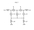
- Fig. 7 is a diagram showing the circuit configuration of a surface acoustic wave filter device in accordance with a second embodiment of the present invention.
- a surface acoustic wave filter element 3 similar to that in accordance with the first embodiment, is used. As shown in Fig. 7 , two series arm resonators 8 and 9, and three parallel arm resonators 10 to 12 are connected to one another so as to have a ladder circuit configuration.
- the ends of the three parallel arm resonators 10 to 12 connected to the ground potential are commonly connected, and inductances L6 and L7 are connected between this commonly connected portion and the external electrodes each connected to an external ground line.
- the ends of the three parallel arm resonators 10 to 12 connected to the ground potential that is, the ground terminals may commonly connected on the piezoelectric substrate.
- Each of the above-described inductances L6 and L7 is defined by a microstrip line formed in the package.
- Fig. 8 is a plan view showing the electrode structure on the top surface of the base board 54 in the package used in the second embodiment.
- the second embodiment is constructed in the same manner as the first embodiment except that the electrode structure on the top surface of the base board 54 of the second embodiment differs from that in the first embodiment.
- the description of the first embodiment will be quoted.
- the surface acoustic wave filter element 3 is bonded via bumps by means of the face down process, in a manner such that the top surface 4a (see Fig. 2 ) of the piezoelectric substrate 4 is placed face down on the area surrounded by broken line X on the top surface of the base board 54.
- a die-attach portion including electrode pads 55 to 57 is formed on the top surface 54a of the base board 54.
- the electrode pads 55 and 56 are bonded to the electrode lands 13 and 17 shown in Fig. 2 via bumps 55a and 56a, respectively.
- the electrode pad 57 is bonded to the electrode lands 14, 15, and 16 connected to the ground potentials shown in Fig. 2 , via bumps 57a to 57d.
- external electrodes 61 to 64 are provided at the corner portions of the base board 54.
- the external electrodes 61 to 64 are formed not only on the top surface 54a of the base board 54, but also so as to extend to the bottom surface through the side surfaces thereof.
- the above-described electrode pads 55 and 56 are connected to the external electrodes 64 and 61 via microstrip lines 65 and 66, respectively.
- the electrode pad 57 is connected to the external electrodes 62 and 63 via the respective microstrip lines 67 and 68.
- the terminals of the three parallel arm resonators connected to the ground potential, via the electrode pad 57 in the die-attach portion of the package 2 are commonly connected, and the electrode pad 57 is connected to the different external electrodes 62 and 63 via the respective microstrip lines 67 and 68.
- the electrode lands 13 and 17 defining input/output signal terminals and the electrode lands 14 to 16 defining ground terminals on the piezoelectric substrate 4, are arranged so as to be rotated by 90° about the normal line passing the center of the piezoelectric substrate 4, with respect to the external electrodes 61 and 64 each connected to the signal line and the external electrodes 62 and 63 each connected to the ground line outside the package.
- microstrip lines 65, 66, 67 and 68 are opposite to the ground electrode 50.
- Other constructions of the second embodiment are the same as those of the first embodiment.
- the attenuation value - frequency characteristics relationship of the surface acoustic wave filter device in accordance with the second embodiment is indicated by a solid line in Fig. 9 .
- the attenuation value - frequency characteristics relationship of the surface acoustic wave filter device in accordance with a conventional example prepared as a comparative example used in the first embodiment is indicated by a broken line.
- each of the inductance components added by the microstrip lines 65 and 66 is set to 0.8 nH, and each of the inductance components added by the microstrip lines 67 and 68 is set to about 0.3 nH.
- the attenuation value in the vicinity of the pass band is increased.
- the width of the pass band corresponding to an attenuation value of 4 dB is 80 MHz for this embodiment, in contrast to 78 MHz for the conventional example, that is, the widening of pass band is simultaneously realized in this embodiment.
- Fig. 10 is a diagram showing the circuit configuration of a surface acoustic wave filter device in accordance with a third embodiment of the present invention.
- the surface acoustic wave filter element 3 is constructed in the same manner as the first embodiment, and two series arm resonators 8 and 9 and three parallel arm resonators 10 to 12 are connected to one another so as to implement a ladder circuit.
- the side wall and the cap member of the package 2 are constructed in the same manner as those of the first embodiment.
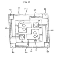
- the difference between the third and first embodiments lies in the electrode structure provided on the base board 74, as shown in Fig. 11 .
- structures other than the electrode structure on the base board 74 descriptions will not be repeated with reference to the description of the first embodiment.
- a plurality of electrode pads 75,76, 77, and 78 are formed, and a die-attach portion is defined by the plurality of electrode pads 75 to 78.
- the portion indicated by a circle or circles inside each of the electrode pads 75 to 78 represents the position of bump when the surface acoustic wave filter element 3 is bonded by means of the face down process.
- External electrodes 81 to 84 are formed at the corners of the base board 74, as is similar with those in the first embodiment.
- the external electrodes 81 and 84 are external electrodes each connected to a signal line, and are connected to the electrode pads 76 and 75 via microstrip lines 86 and 85.
- the electrode pads 77 and 78 are connected to the external electrode 82 and 83 each connected to a ground line, via microstrip lines 87 and 88.
- the electrode pad 75 is connected to the electrode lands 13 shown in Fig. 2 via a bump 75a
- the electrode pad 76 is connected to the electrode land 17 shown in Fig. 2 via a bump 76a
- the electrode pad 77 is connected to the electrode lands 14 ( Fig. 2 ) via bumps 77a and 77b
- the electrode pad 78 is connected to the electrode lands 15 and 16 (see Fig. 2 ) via bumps 78a and 78b.
- ground terminals of at least two parallel arm resonators may be connected to one electrode land.
- electrode lands connected to the ground potential, for example, the electrode lands 15 and 16 may be made a common land.
- the first parallel arm resonator 10 and the second and third resonators 11 and 12 are separated from each other in the die-attach portion.
- An inductance L7 by the microstrip line 87 is defined between the first parallel arm resonator 10 and the external electrode 82 connected to an external ground line
- an inductance L8 by the microstrip line 88 is defined between the second and third parallel arm resonators 11 and 12 and the external electrode 83 connected to a ground line.
- the attenuation value - frequency characteristics relationship of the surface acoustic wave filter device in accordance with the third embodiment is shown in Fig. 12 using a solid line.
- the attenuation value - frequency characteristics relationship of the surface acoustic wave filter device in accordance with the conventional example prepared for comparison used in the first embodiment is shown in Fig. 12 using a broken line.
- each of the inductance components by the microstrip lines 85 and 86 was set to 0.8 nH, and each of the inductance components by the microstrip lines 87 and 88 was set to about 0.3 nH.
- Other constructions of this embodiment is similar to those of the first embodiment.
- the attenuation value in the vicinity of the pass band can be significantly increased over the conventional example, since inductance components are formed in the package 2 by the above-described microstrip lines 85 to 88.
- the width of the pass band corresponding to an attenuation value of 4 dB, is 85 MHz for this embodiment, in contrast to 78 MHz for the conventional example, that is, the widening of pass band is simultaneously realized in this embodiment.
- the frequency at the attenuation pole fr in the vicinity of the pass band is increased. Therefore, when an increase in the attenuation value in the frequency range nearer to the pass band is required, the surface acoustic wave filter device in accordance with the third embodiment is more advantageous than that in accordance with the second embodiment.
- Fig. 13 is a diagram showing the circuit configuration of a surface acoustic wave filter device in accordance with a fourth embodiment of the present invention.
- the same surface acoustic wave filter element 3 as that in accordance with the first embodiment is used, and first and second series arm resonators 8 and 9, and parallel arm resonators 10 to 12 are connected to one another so as to have a ladder circuit.
- a package 2 includes a base board 94 as a first case member. Also, a second case member including a side wall 95 and a cap 96, is constructed as in the same manner as that in the first embodiment.
- the base board 94 is constructed by a laminated ceramic board including substrates 94b, 94c and 94d, and within the base board 94, microstrip lines for adding inductances as described later are formed.
- Fig. 15 is a plan view showing a top surface of the base board 94 and a top surface of the substrate 94b
- Fig. 16 is a plan view showing a top surface of the substrate 94c where microstrip lines are formed.
- electrode pads 55 to 57 are formed on the top surface of the base board 94, in the same manner as the base board in the second embodiment shown in Fig. 8 . In this embodiment, however, no external electrode and microstrip line are formed on the top surface of the base board 94, and are provided inside the base substrate 94.
- Through hole electrodes 95a to 95d penetrating through the substrate 94b and reaching the bottom surface thereof are provided at the electrode pads 55 to 57.
- the lower ends of the through hole electrodes 95a to 95d are connected to one-side ends of the microstrip lines 97a to 97d provided on the upper surface of the substrate 94c, respectively.
- the other ends of the microstrip lines 97a to 97d are connected to the external electrodes 98a to 98d on the upper surface of the substrate 94c, respectively.
- the external electrodes 98a to 98d are formed so as to extend from the corner portions to the bottom surface of the base board 94 through the side surfaces of the substrates 94c and 94d (see Fig. 14 ).
- the ground electrode 50 for microstrip lines 97a to 97d is provided to cover the substantially entire bottom surface of the substrate 94c.
- the microstrip lines 97a to 97d are embedded in the base board 94 as the first case member, and by these microstrip lines 97a to 97d, as shown in Fig. 13 , inductance components L9 and L10 are defined between the portion where the first to third parallel arm resonators are commonly connected, and the external electrodes each connected to an external ground line, while inductance components L1 and L2 are defined between the series arm resonators 8 and 9 and the external electrodes each connected to an external signal line.
- microstrip lines for adding inductances can be formed at any positions within the package.
- the solid line in Fig. 17 shows the attenuation value - frequency characteristics relationship of the surface acoustic wave filter device in accordance with the fourth embodiment
- the broken line shows the attenuation value - frequency characteristics relationship of the surface acoustic wave filter device in accordance with the conventional example prepared for comparison.
- the inductance component by a microstrip line added to each of the series arm resonators was set to 1.0 nH
- the inductance components L9 and L10 each connected between the parallel arm resonator and the ground line was set to 1.0 nH.
- a formation of microstrip lines for adding inductance components increases the attenuation value in the vicinity of the pass band.
- the improvement in the attenuation value on the lower frequency side is significant. This is because the frequency fr of the attenuation pole has become lower since the value of the inductances L8 and L9 connected in parallel with each other are large.
- each of the microstrip lines can be lengthened, thereby providing a larger inductance value.
- inductance components by microstrip lines are each connected to at least any of the series arm resonators and parallel arm resonators constituting a ladder circuit, and the microstrip lines are disposed in the package, the attenuation value in the vicinity of the pass band is increased and wide-band filter characteristics can be achieved.
- the package comprises a die-attach portion having a plurality of electrode pads each of which is connected to any one of the signal terminals and any one of the ground terminals of the surface acoustic wave filter element by the bumps; and a plurality of external electrodes each of which is electrically connected to any one of the electrode pads, and each of which is connected to a signal line or a ground line outside the surface acoustic wave filter device
- the surface acoustic wave filter element can be reliably connected and mechanically bonded to the plurality of electrode pads using bumps by means of face down process.
- the present invention therefore, allows a wide-band filter device which is large in the attenuation value outside the pass band to be easily formed.
- each of the microstrip lines is connected between the electrode pad connected to the signal terminal of the series arm resonator and the external electrode connected to the signal line outside the surface acoustic wave filter device, since each of the microstrip lines is connected between the series arm resonator and the signal line, the reflection loss can be reduced and the widening of pass band can be achieved.
- the surface acoustic wave filter device comprises at least two parallel arm resonators, wherein the ground terminals of all the parallel arm resonators are commonly connected, on the piezoelectric substrate, wherein each of the microstrip lines is connected between the portion where the ground terminals of the parallel arm resonators are commonly connected, and each of the external electrodes provided in the package, the attenuation value can be increased at lower frequency range.
- the attenuation value can be increased at lower frequency range, as well.
- making the electrode pads a common pad on the package side facilitates the wiring of chips.
- the surface acoustic wave filter comprises at least three parallel arm resonators, wherein microstrip lines are provided on the path between the electrode lands to which the ground terminals of at least two parallel arm resonators are connected, and the external electrodes to which these electrode lands are connected, and wherein the parallel arm resonators other than the above-described at least two parallel arm resonators are, on the piezoelectric substrate, electrically isolated from the above-described at least two parallel arm resonators, it is possible to obtain filter characteristics wherein more widening of pass band is achieved and simultaneously the attenuation value in the vicinity of the pass band is increased.
- the surface acoustic wave filter device comprises at least three parallel arm resonators; and a common electrode pad connected to the ground terminals of at least two parallel arm resonators among the parallel arm resonators, wherein each of the microstrip lines is provided on the path between the common electrode pad and the external electrodes to which the common electrode pad is connected, and wherein the other parallel arm resonators are electrically isolated from the above-described at least two parallel arm resonators, at a die-attach portion including a plurality of electrode pads, the attenuation value in the vicinity of the pass band is more increased, and wideband filter characteristics can be implemented.
- the microstrip lines are disposed, in the package, at the positions other than the position of the die-attach portion, the electromagnetic interference with the surface acoustic wave filter element, and consequently, the deterioration of filter characteristics is prevented.
- the package comprises a base board, an annular side wall provided on the base board, and a cap member affixed to the annual side wall so as to close the upper end thereof, wherein the main portion of each of the microstrip lines is disposed between the side wall and the base board, there is no need for extra space, so that filter characteristics can be improved without changing the size of the package.
- the package comprises the first case member on which the surface acoustic wave filter element is mounted, and the second case member enclosing the surface acoustic wave filter element mounted on the first case member, wherein the main portion of each of the microstrip lines is provided inside the first case member, it becomes possible to insert large inductance components, resulting in a significant improvement in filter characteristics.
- the signal terminals at the input/output ends of the surface acoustic wave filter element and at least one ground terminal thereof are disposed so as to be rotated by 90° around the imaginary line which passes the center of the piezoelectric substrate of the surface acoustic wave filter element, and which is perpendicular to the piezoelectric substrate, with respect to the external electrodes connected to the input/output end signal lines and at least one external electrode connected to the ground potential among the plurality of external electrodes, it becomes possible to insert large inductance components without making troublesome bending portions, when forming microstrip lines between the side wall and the base board.
- the surface acoustic wave filter device can be applied to various communication apparatuses and signal processing devices, in particular, to a small communication apparatus such as portable phone.
Abstract
Description
- The present invention relates to a surface acoustic wave filter, and particularly to a surface acoustic wave filter device having a ladder type circuit.
- There has been known a band-pass filter having a ladder type circuit wherein a plurality of one terminal pair surface acoustic wave resonators are connected in ladder shape (e.g., Japanese Unexamined Patent Application Publication No.
05-183380 - In this band-pass filter, a plurality of one terminal pair surface acoustic wave resonators are connected in series between input terminal and output terminal as series arm resonators, and define series arms. In addition, a plurality of one terminal pair surface acoustic wave resonators are connected in parallel between the series arms and ground as parallel arm resonators, and define parallel arms.
- The band-pass filter having the ladder type circuit has small insertion loss and wide pass band, and is widely used as a band-pass filter in a portable telephone
- The Japanese Unexamined Patent Application Publication No.
05-183380 - Also, the Japanese Unexamined Patent Application Publication No.
10-93382 Fig. 18 shows a circuit configuration of the surface acoustic wave filter device disclosed in this prior art. In the surface acousticwave filter device 501, series arm resonators S1 and S2 and parallel arm resonators P1 to P3 are connected to one another so as to constitute a ladder type circuit. Here, an inductance L is inserted between the parallel arm resonators P1 to P3 and the ground potential, and thereby the widening of pass band and the increase in attenuation value in the vicinity of a pass band are achieved. - On the other hand, Japanese Unexamined Patent Application Publication No.
04-65909 Fig. 19 shows a schematic sectional view of a package of a surface acoustic wave filter element accommodated by using this face down process. - In the surface acoustic
wave filter device 601, a surface acousticwave filter element 603 is accommodated in apackage 602. Thepackage 602 includes abase board 602a, aside wall 602b, and acap 602c. - On the
base board 602a, there is formed a die-attach portion 602d having a plurality of electrode pads electrically connected to the surface acousticwave filter element 603. The surface acousticwave filter element 603 has a piezoelectric substrate 603a, and electrodes for constructing surface acoustic wave filter element are formed on the bottom surface of the piezoelectric substrate 603a. The electrodes formed on the bottom surface of the piezoelectric substrate 603a are electrically connected to the electrode pads in the die-attach portion 602d viabumps 604, and the surface acousticwave filter element 603 is mechanically fixed to the die-attach portion 602d by thebumps 604. - Since such a face down process, that is, in a method of bonding a surface where electrodes constituting a surface acoustic wave filter element of the piezoelectric substrate is formed to a package by bumps, since no bonding wire is required, a small surface acoustic wave filter device can be produced.
- As disclosed in the Japanese Unexamined Patent Application Publications Nos.
05-183380 10-93382 - However, in the surface acoustic
wave filter device 601, which is packaged by above-described face down process, since no bonding wire is provided, an inductance component can not be added to the surface acousticwave filter device 601 by the bonding wire. it is possible to obtain a small inductance component by rooting electrodes connecting the external electrodes provided on the package and the die-attach portion, but a large inductance can not be obtained by such rooting electrodes. - Therefore, in the surface acoustic wave filter device disclosed in the Japanese Unexamined Patent Application Publication No.
04-65909 - The Japanese Unexamined Patent Application Publication No.
04-65909 - Also, in the Japanese Unexamined Patent Application Publication No.
04-65909 - The object of the present invention is to overcome the above-described drawbacks of the prior art, and to provide a surface acoustic wave filter device with excellent filter characteristics, in which a surface acoustic wave filter element having a ladder type circuit is accommodated in a package by means of the face down process. Inductances are added to parallel arm resonators and/or series arm resonators, and the deterioration of filter characteristics by the electromagnetic coupling between the electrodes on the surface acoustic wave filter element and the inductances provided in the package hardly occurs. The limitations on the position and the number of bumps is low.
- In accordance with a broad aspect of the present invention, there is provided a surface acoustic wave filter device, comprising a surface acoustic wave filter element which includes a piezoelectric substrate and a plurality of one terminal pair surface acoustic wave elements formed on the piezoelectric substrate, and in which the one terminal pair surface acoustic wave elements are connected so as to define a parallel arm resonator and a series arm resonator in a ladder circuit; and a package accommodating the surface acoustic wave filter element. In this surface acoustic wave filter device, the surface acoustic wave filter element is bonded via a plurality of bumps by means of the face down process and is accommodated in the package. This surface acoustic wave filter device further comprises an inductance component of a microstrip line which is provided in said package and connected to at least one of the series arm resonator and the parallel arm resonator.
- In accordance with a specific aspect of the present invention, the above-described package includes a die-attach portion including a plurality of electrode pads which are connected via the bumps to one of a signal terminal and a ground terminal of the surface acoustic wave filter element; and a plurality of external electrodes which are electrically connected to at least one of the electrode pads, and connected to one of a signal line and a ground line outside the surface acoustic wave filter device.
- In accordance with a more restrictive aspect of the present invention, the above described microstrip line is connected between the electrode pad connected to the signal terminal of the series arm resonator and the external electrode connected to the signal line outside the surface acoustic wave filter device.
- In accordance with another restrictive aspect of the present invention, the above-described microstrip line is provided between the electrode pad connected to the ground terminal of at least one parallel arm resonator via the bumps, and the external electrode which is connected to the ground line outside the package.
- In accordance with another particular aspect of the present invention, the surface acoustic wave filter device in accordance with the present invention comprises at least two parallel arm resonators. In this surface acoustic wave filter device, the ground terminals of all the parallel arm resonators are commonly connected on the piezoelectric substrate, and the microstrip line is connected between the portion where the ground terminals of the parallel arm resonators are commonly connected and the external electrode provided in the package.
- In accordance with still another particular aspect of the present invention, the surface acoustic wave filter device in accordance with the present invention comprises at least two parallel arm resonators. In this surface acoustic wave filter device, the package-side electrode pads connected to the ground terminals of all the parallel arm resonators, are made a common electrode pad, and the microstrip line is provided on the path between the common electrode pad and the external electrode.
- In accordance with still another restrictive aspect of the present invention, the surface acoustic wave filter device in accordance with the present invention comprises at least three parallel arm resonators; and an electrode land which is provided on the piezoelectric substrate, and to which the ground terminals of at least two parallel arm resonators are each connected. In this surface acoustic wave filter device, the microstrip line is provided on the path between the electrode land connected to the ground terminals of at least two parallel arm resonators and the external electrode to which the electrode land is connected; and the parallel arm resonator other than the above-described at least two parallel arm resonators is electrically isolated from the above-described at least two parallel arm resonators on the piezoelectric substrate, and is electrically connected to the external electrode other than the package-side external electrode connected to the above-described at least two parallel arm resonators.
- In accordance with a further particular aspect of the present invention, the surface acoustic wave filter device in accordance with the present invention comprises at least three parallel arm resonators. In this surface acoustic wave filter device, the plurality of electrode pads include a common electrode pad connected to the ground terminals of at least two parallel arm resonators among the parallel arm resonators, and the microstrip line is provided on the path between the common electrode pad and the external electrode to which the common electrode pad is connected; and the parallel arm resonator other than the above-described at least two parallel arm resonators is electrically isolated from the above-described at least two parallel arm resonators, at a die-attach portion including the plurality of electrode pads, and is electrically connected to the external electrode other than the package-side external electrode connected to the above-described at least two parallel arm resonators.
- In accordance with a further restrictive aspect of the present invention, the above-described microstrip line is disposed in the package at the position other than the position of the die-attach portion.
- In accordance with a yet further particular aspect of the present invention, the above-described package comprises a base board on which the surface acoustic wave filter element is mounted; an annular side wall provided on the base board; and a cap member attached to the annual side wall so as to close the upper end thereof. Herein, a main portion of the microstrip line is disposed between the side wall and the base board.
- In accordance with another particular aspect of the present invention, the above-described package comprises a first case member on which the surface acoustic wave filter element is mounted; and a second case member enclosing the surface acoustic wave filter element mounted on the first case member. Herein, a main portion of the microstrip line is provided inside the first case member.
- Here, "a main portion of a microstrip line" refers to at least 50% of the entire length of a microstrip line.
- In accordance with still another particular aspect of the present invention, the signal terminal at the input/output end of the surface acoustic wave filter element and at least one ground terminal thereof are arranged so as to be rotated by 90° about the imaginary line which passes the center of the piezoelectric substrate of the surface acoustic wave filter element, and which is perpendicular to the piezoelectric substrate, with respect to the external electrode connected to the signal line at the input/output end and the external electrode connected to at least one ground potential among the plurality of external electrodes.
- The communication device in accordance with the present invention is characterized by comprising a surface acoustic wave filter device in accordance with the present invention.
-
-
Fig. 1 is a schematic sectional view of a surface acoustic wave filter device in accordance with a first embodiment of the present invention. -
Fig. 2 is a plan view showing an electrode structure of a surface acoustic wave filter element used in the surface acoustic wave filter device in accordance with the first embodiment of the present invention. -
Fig. 3 is a schematic plan view showing a die-attach portion including a plurality of electrode pads on the top surface of a base board in a package of the surface acoustic wave filter device in accordance with the first embodiment of the present invention. -
Fig. 4 is a circuit diagram of the surface acoustic wave filter device in accordance with the first embodiment. -
Fig. 5 is a plan view showing an electrode pattern on the top surface of the base board in the package of a conventional surface acoustic wave filter device prepared for comparison. -
Fig. 6 is a diagram showing the attenuation value - frequency characteristics relationships in the surface acoustic wave device of the first embodiment and that of the conventional example. -
Fig. 7 is a circuit diagram of a surface acoustic wave filter device in accordance with a second embodiment of the present invention. -
Fig. 8 is a plan view showing an electrode structure on the top surface of a base board in a package used in a surface acoustic wave filter device in accordance with the second embodiment. -
Fig. 9 is a diagram showing the attenuation value - frequency characteristics relationships in the surface acoustic wave filter device of the second embodiment and that of the conventional example. -
Fig. 10 is a circuit diagram of a surface acoustic wave filter device in accordance with a third embodiment of the present invention. -
Fig. 11 is a plan view showing an electrode structure on the top surface of a base board in a package used in a surface acoustic wave filter device in accordance with the third embodiment. -
Fig. 12 is a diagram showing the attenuation value - frequency characteristics relationships in the surface acoustic wave filter device of the third embodiment and that of the conventional example. -
Fig. 13 is a circuit diagram of a surface acoustic wave filter device in accordance with a fourth embodiment of the present invention. -
Fig. 14 is a schematic sectional view of a surface acoustic wave filter device in accordance with the fourth embodiment of the present invention. -
Fig. 15 is a plan view showing an electrode structure on the top surface of a base board in a package used in a surface acoustic wave filter device in accordance with the fourth embodiment. -
Fig. 16 is a plan view showing the electrode structure within the base board in the package used in the surface acoustic wave filter device in accordance with the fourth embodiment of the present invention. -
Fig. 17 is a diagram showing the attenuation value - frequency characteristics relationships in the surface acoustic wave filter device of the fourth embodiment and that of the conventional example. -
Fig. 18 is a circuit diagram showing an example of a surface acoustic wave filter device having a conventional ladder type circuit. -
Fig. 19 is a sectional view showing another example of a conventional surface acoustic wave filter device. - Hereinafter, the surface acoustic wave filter device in accordance with the present invention will be described in detail with reference to the drawings.
- As shown in
Fig. 1 , the surface acousticwave filter device 1 in accordance with the present embodiment includes apackage 2, and a surface acousticwave filter element 3 accommodated in apackage 2.Fig. 1 only schematically shows an appearance of the surface acousticwave filter device 3. - The
package 2 comprises abase board 4 having a rectangular plate shape, a rectangular frame-shapedside wall 5 bonded on thebase board 4, and a rectangular plate-shapedcap member 6 affixed to theside wall 5 so as to close the upper opening thereof. Theside wall 5 does not necessarily requires to be rectangular, but may have a ringshaped structure such as annular shape. - The
base board 4 and theside wall 5 may be made of an insulative ceramic such as alumina, or a synthetic resin. Thecap member 6 may also be made of a similar material. Alternatively, thecap member 6 may be made of a metal or the like in order to have an electromagnetic shielding property. - The
base board 4 is constructed by a multilayersubstrate including substrates substrate 4a and thesubstrate 4b, aground electrode 50 for microstrip line which is described later is provided on a substantially entire surface of thesubstrate 4b. Thesubstrates - As shown in
Fig. 2 , the surface acousticwave filter element 3 has a rectangular plate-shaped piezoelectric substrate 7 as a piezoelectric substrate. In this embodiment, the piezoelectric substrate 7 is made of a 36°, Y-cut, and X-propagation LiTaO3 substrate. The piezoelectric substrate 7, however, may be made of another piezoelectric single crystal, or a piezoelectric ceramic such as lead titanate zirconate-based ceramic. Alternatively, a piezoelectric substrate constructed by forming a piezoelectric thin film made of ZnO or the like, on a piezoelectric plate or an insulating substrate, may be employed. - A metallic film is formed over the entire
top surface 7a of the piezoelectric substrate 7, and then an electrode pattern shown in the figure is formed by the photolithography and etching. A metallic material for forming the electrode pattern is not particularly limited, but in this embodiment, aluminum is used as a metallic material. The formation of an electrode may also be performed using the lithography and lift off method. - The above-described electrode pattern will be described with reference to
Fig. 2 . - On the
top surface 7a of the piezoelectric substrate 7, in order to implement a ladder circuit,series arm resonators parallel arm resonators 10 to 12 each of which includes one terminal pair surface acoustic wave element are formed. Each of theseries arm resonators parallel arm resonators 10 to 12 has one IDT and reflectors disposed on the opposite sides of each the IDTs in the propagation direction of a surface acoustic wave. Taking theseries arm resonator 8 as a representative example, theseries arm resonator 8 includes an IDT 8a and a pair ofreflectors - Also, on the
top surface 7a of the piezoelectric substrate 7, electrode lands 13 to 17 are formed. Each of the electrode lands 13 to 17 is a portion for electrically connecting the surface acousticwave filter element 3 to the outside, and is formed of a metallic film having an area to a certain extent. Here, the circular portions drawn in the electrode lands 13 to 17 represent the portions to be bonded by the bumps. - The electrode lands 13 is used as the input end of the surface acoustic
wave filter element 3, and is connected to one end of the firstseries arm resonator 8 via aconductive path 18. Theconductive path 18 electrically connects theelectrode land 13, the one end of theseries arm resonator 8, and one end of the firstparallel arm resonator 10. An end of theparallel arm resonator 10 which is opposite to the end thereof connected to theconductive path 18 is connected to theelectrode land 14 via aconductive path 19. Theelectrode land 14 is an electrode land connected to the ground potential. - Also, an end of the
series arm resonator 8 which is opposite to the end thereof connected to theconductive path 18 is connected to aconductive path 20. Theconductive path 20 is connected to one end of the secondseries arm resonator 9 and also to one end of the secondparallel arm resonator 11. An end of the secondparallel arm resonator 11 which is opposite to the end thereof connected to theconductive path 20 is connected to anelectrode land 15. Theelectrode land 15 is an electrode land connected to the ground potential. - A
conductive path 21 is connected to the other end of the secondseries arm resonator 9. Theconductive path 21 is also connected to theelectrode land 17 and one end of the thirdparallel arm resonator 12. Theelectrode land 17 is used as an output terminal. An end of theparallel arm resonator 12 which is opposite to the end thereof connected to theconductive path 21 is connected to an electrode land 16 via aconductive path 22. The electrode land 16 is an electrode land connected to the ground potential. - In the surface acoustic
wave filter element 3, therefore, the above-described first and secondseries arm resonators Fig. 4 . Meanwhile, inductances L1 to L5 inFig. 4 will be described later. -
Fig. 3 illustrates the electrode structure formed on the top surface of thebase board 4 in thepackage 2 shown inFig. 1 . - The surface acoustic
wave filter element 3 is mounted on the portion indicated by a broken line X on thetop surface 4a of thebase board 4. At this portion, the above-described surface acousticwave filter element 3 is bonded by bumps in a manner such that thetop surface 7a of the piezoelectric substrate 7 is placed face down. More specifically, the surface acousticwave filter element 3 shown inFig. 2 is superposed on thetop surface 4a of thebase board 4 shown inFig. 3 , in a manner such that thetop surface 7a of the piezoelectric substrate 7 is placed face down, and the surface acousticwave filter element 3 and thebase board 4 are bonded by bumps, thereby fixing the surface acousticwave filter element 3. - On the
top surface 4a of thebase board 4, electrodes shown in the figure are formed by printing and firing electrode paste. The plurality ofelectrode pads 23 to 27 define a die-attach portion. Theelectrode pads 23 to 27 are formed separately from one another. Among these, theelectrode pad 23 is electrically connected to theelectrode land 13 shown inFig. 2 and mechanically bonded thereto, by abump 28. Likewise, theelectrode pads 24 to 26 are connected to the electrode lands 14 to 16 shown inFig. 2 , respectively, bybumps electrode pad 27 is electrically connected to theelectrode land 17 shown inFig. 2 via a bump 32. - Among the above-described
electrode pads 23 to 27, theelectrode pads electrode pad -
External electrodes 41 to 44 are formed on the top surface of thebase board 4. Theexternal electrodes 41 to 44 are formed not only on thetop surface 4a of thebase board 4, but also so as to extend to the bottom surface and the side surfaces thereof, at portions which are not shown inFig. 1 . Each of theexternal electrodes 41 to 44 thus performs the function of an electrode for electrically connecting the surface acousticwave filter device 1 to the outside. - The
external electrode 44 is connected to theelectrode pad 23 via amicrostrip line 45. Likewise, theexternal electrode 41 is connected to theelectrode pad 27 via amicrostrip line 46. Also, theexternal electrode 42 is connected to theelectrode pad 24 via amicrostrip line 47, and theexternal electrode 43 is connected to bothelectrode pads microstrip lines - The
external electrodes external electrodes - The above-described
microstrip lines 45 to 49 are opposite to theground electrode 50 via thesubstrate 4b, as indicated by broken line inFig. 3 . Fine belt-shaped conductive patterns function as microstrip lines. InFig. 3 , though theground electrode 50 is provided on a substantially entire surface of thesubstrate 4b,ground electrode 50 may be formed at portions opposite to themicrostrip lines 45 to 49. The above-describedmicrostrip lines 45 to 49 located between thebase board 4 and the side wall. - In this embodiment, inductance components are obtained by the above-described
microstrip lines 45 to 49. Specifically, an inductance L1 shown inFig. 4 is defined by themicrostrip line 45, an inductance L2 is defined by themicrostrip line 46, and inductances L3 to L5 are defined by themicrostrip lines 47 to 49, respectively. - In other words, inductance components of the
microstrip lines 47 to 49 are each connected between parallel arm resonators having a ladder circuit, and the external electrodes each connected to the ground line. Likewise, inductance components of themicrostrip lines external electrodes - In this embodiment, in the surface acoustic wave filter device including a ladder type filter circuit comprising two
series arm resonators parallel arm resonators 10 to 12, inductance components are independently added into theparallel arm resonators 10 to 12 by the above-describedmicrostrip lines 47 to 49, respectively. This allows the widening of pass band and the increase in attenuation value in the vicinity of pass band. This will be described based on specific experimentation. - The solid line in
Fig. 6 shows the attenuation value - frequency characteristics relationship of the surface acoustic wave filter device in accordance with the present invention, and the broken line shows that of a surface acoustic wave filter device prepared for comparison. - The conventional surface acoustic wave filter device, the results of which are shown in
Fig. 6 by the broken line, is the same as that of the above-described embodiment except that the electrode structure on the top surface of the base board of the package has been formed as shown inFig. 5 . That is,electrode pads 105 to 107 are formed on the top surface 104a of abase board 104.External electrodes 111 to 114 are formed at the four corners. Theexternal electrodes 111 to 114 are formed so as to extend from the top surface to the bottom surface through the side surfaces thereof. These external electrodes corresponds to the portions which are electrically connected to the outside. Theexternal electrodes electrode pads conductive paths - Since ground electrodes are not formed on portions of the
base board 104 which is opposite to theconductive paths conductive paths electrode pad 107 having a large area is directly connected toexternal electrodes electrode pad 107 is bonded via bumps to the electrode lands 14 to 16 of the surface acousticwave filter element 3 each connected to the ground line, and theelectrode pads - Therefore, in the conventional surface acoustic wave filter device prepared for comparison, there are no microstrip lines independently formed between the
parallel arm resonators 10 to 12 and theexternal electrodes series arm resonators external electrodes - The specifications of the surface acoustic
wave filter element 3 used in the above-described embodiment and the conventional example are as follows: - The
series arm resonators - The first and third
parallel arm resonators - The second
parallel arm resonators 11 ...... interdigital width of electrode finger = 52 µm, number of pairs of electrodes in an IDT = 90, number of electrode fingers in a reflector = 100, and electrode finger pitch = 1.04 µm (wavelength of surface acoustic wave λ = 2.08 µm). - In the embodiment, the inductance components by the
microstrip lines 45 to 49 formed on thebase board 4, are as follows: - Microstrip lines 45 and 46 ...... 0.8 nH
- Microstrip lines 47 and 49 ...... 0.8 nH
-
Microstrip line 48 ...... 0.5 nH - As can be seen from
Fig. 6 , the width of the pass band corresponding to an attenuation value of 4 dB, is 86 MHz for this embodiment, in contrast to 78 MHz for the conventional example, that is, this embodiment exhibits a wider pass band width than the conventional example. The attenuation pole in the vicinity of the pass band, in this embodiment, is positioned at substantially the same frequency as that in the conventional example. This would be because there exists no common inductance component since the electrode pads of the die-attach portion connected to the ground potential are separated from one another, in other words, since inductance components are independently added to the first to thirdparallel arm resonators 10 to 12 by the above-describedmicrostrip lines 47 to 49. - Furthermore, it will be recognized that, since the
microstrip lines 45 to 49 for adding the above-described inductance components exist between the base board and the side wall, the electromagnetic coupling between each of themicrostrip lines 45 to 49 and the surface acousticwave filter element 3 does not much occur, so that superior filter characteristics can be achieved. In addition, since the above-describedmicrostrip lines 45 to 49 do not exist in the die-attach portion, there is no risk that these microstrip lines impose limitations on the position and the number of bumps. This allows the surface acousticwave filter element 3 to be bonded to thebase board 4 with a sufficient bonding strength. - Changing the dielectric constant of the
substrate 4b on which the microstrip lines are provided, and the distance between the microstrip lines and theground electrode 50 makes it possible to design the inductance component per unit length of the microstrip line. Therefore, necessary inductance component in order to improve the characteristics of surface acoustic wave filter can be designed and added into the surface acoustic wave filter with use of the inductance component of microstrip line. Further, since the microstrip line is resistant to the influence from outside, the inductance component of the microstrip line hardly changes even if the surface acoustic wave filter element is attached to the base board by face down process. Therefore desired inductance component is added to the surface acoustic wave filter to be in line with the design. -
Fig. 7 is a diagram showing the circuit configuration of a surface acoustic wave filter device in accordance with a second embodiment of the present invention. - In this embodiment also, a surface acoustic
wave filter element 3 similar to that in accordance with the first embodiment, is used. As shown inFig. 7 , twoseries arm resonators parallel arm resonators 10 to 12 are connected to one another so as to have a ladder circuit configuration. - As seen from
Fig. 7 , however, in this embodiment, the ends of the threeparallel arm resonators 10 to 12 connected to the ground potential are commonly connected, and inductances L6 and L7 are connected between this commonly connected portion and the external electrodes each connected to an external ground line. Here, the ends of the threeparallel arm resonators 10 to 12 connected to the ground potential, that is, the ground terminals may commonly connected on the piezoelectric substrate. - Each of the above-described inductances L6 and L7 is defined by a microstrip line formed in the package.
-
Fig. 8 is a plan view showing the electrode structure on the top surface of thebase board 54 in the package used in the second embodiment. - The second embodiment is constructed in the same manner as the first embodiment except that the electrode structure on the top surface of the
base board 54 of the second embodiment differs from that in the first embodiment. Hence, with regard to the structure of the surface acousticwave filter element 3 and other structures of thepackage 2, the description of the first embodiment will be quoted. - In this embodiment also, the surface acoustic
wave filter element 3 is bonded via bumps by means of the face down process, in a manner such that thetop surface 4a (seeFig. 2 ) of thepiezoelectric substrate 4 is placed face down on the area surrounded by broken line X on the top surface of thebase board 54. - A die-attach portion including
electrode pads 55 to 57 is formed on thetop surface 54a of thebase board 54. Theelectrode pads Fig. 2 viabumps electrode pad 57 is bonded to the electrode lands 14, 15, and 16 connected to the ground potentials shown inFig. 2 , viabumps 57a to 57d. - As in the case of the first embodiment,
external electrodes 61 to 64 are provided at the corner portions of thebase board 54. Theexternal electrodes 61 to 64 are formed not only on thetop surface 54a of thebase board 54, but also so as to extend to the bottom surface through the side surfaces thereof. The above-describedelectrode pads external electrodes microstrip lines electrode pad 57 is connected to theexternal electrodes respective microstrip lines - That is, the terminals of the three parallel arm resonators connected to the ground potential, via the
electrode pad 57 in the die-attach portion of thepackage 2 are commonly connected, and theelectrode pad 57 is connected to the differentexternal electrodes respective microstrip lines - The electrode lands 13 and 17 defining input/output signal terminals and the electrode lands 14 to 16 defining ground terminals on the
piezoelectric substrate 4, are arranged so as to be rotated by 90° about the normal line passing the center of thepiezoelectric substrate 4, with respect to theexternal electrodes external electrodes - As is similar with the first embodiment, the
microstrip lines ground electrode 50. Other constructions of the second embodiment are the same as those of the first embodiment. - The attenuation value - frequency characteristics relationship of the surface acoustic wave filter device in accordance with the second embodiment is indicated by a solid line in
Fig. 9 . For comparison, the attenuation value - frequency characteristics relationship of the surface acoustic wave filter device in accordance with a conventional example prepared as a comparative example used in the first embodiment, is indicated by a broken line. - In the embodiment, each of the inductance components added by the
microstrip lines microstrip lines - Actually, however, this results in that a common inductance of about 0.1 nH is inserted, since the
microstrip lines external electrodes - As can be seen from
Fig. 9 , in this embodiment, since inductance components are added in thepackage 2 by the above-describedmicrostrip lines 65 to 68, the attenuation value in the vicinity of the pass band is increased. The width of the pass band corresponding to an attenuation value of 4 dB, is 80 MHz for this embodiment, in contrast to 78 MHz for the conventional example, that is, the widening of pass band is simultaneously realized in this embodiment. - In this embodiment also, since microstrip lines for adding inductances exist between the
base board 4 and theannular side wall 5, the electromagnetic coupling with the surface acoustic wave filter element is low, thereby providing superior filter characteristics. Furthermore, as in the case of the first embodiment, in this embodiment also, since no microstrip lines exist in the die-attach portion, there is no limitations on the position and the number of bumps. This enables the surface acousticwave filter element 3 to be securely bonded to thebase board 4. -
Fig. 10 is a diagram showing the circuit configuration of a surface acoustic wave filter device in accordance with a third embodiment of the present invention. In the third embodiment also, the surface acousticwave filter element 3 is constructed in the same manner as the first embodiment, and twoseries arm resonators parallel arm resonators 10 to 12 are connected to one another so as to implement a ladder circuit. - In this embodiment also, the side wall and the cap member of the
package 2 are constructed in the same manner as those of the first embodiment. The difference between the third and first embodiments lies in the electrode structure provided on thebase board 74, as shown inFig. 11 . Hence, with regard to structures other than the electrode structure on thebase board 74, descriptions will not be repeated with reference to the description of the first embodiment. - On the
top surface 74a of thebase board 74, a plurality ofelectrode pads electrode pads 75 to 78. The portion indicated by a circle or circles inside each of theelectrode pads 75 to 78 represents the position of bump when the surface acousticwave filter element 3 is bonded by means of the face down process. -
External electrodes 81 to 84 are formed at the corners of thebase board 74, as is similar with those in the first embodiment. Theexternal electrodes electrode pads microstrip lines electrode pads external electrode microstrip lines - Also, the
electrode pad 75 is connected to the electrode lands 13 shown inFig. 2 via a bump 75a, and theelectrode pad 76 is connected to theelectrode land 17 shown inFig. 2 via abump 76a. Theelectrode pad 77 is connected to the electrode lands 14 (Fig. 2 ) viabumps 77a and 77b, and theelectrode pad 78 is connected to the electrode lands 15 and 16 (seeFig. 2 ) viabumps - As shown in
Fig. 10 , therefore, the firstparallel arm resonator 10 and the second andthird resonators microstrip line 87 is defined between the firstparallel arm resonator 10 and theexternal electrode 82 connected to an external ground line, and an inductance L8 by themicrostrip line 88 is defined between the second and thirdparallel arm resonators external electrode 83 connected to a ground line. - The attenuation value - frequency characteristics relationship of the surface acoustic wave filter device in accordance with the third embodiment is shown in
Fig. 12 using a solid line. For comparison, the attenuation value - frequency characteristics relationship of the surface acoustic wave filter device in accordance with the conventional example prepared for comparison used in the first embodiment, is shown inFig. 12 using a broken line. - In this case, each of the inductance components by the
microstrip lines microstrip lines - As can be seen from
Fig. 12 , in this embodiment also, the attenuation value in the vicinity of the pass band can be significantly increased over the conventional example, since inductance components are formed in thepackage 2 by the above-describedmicrostrip lines 85 to 88. The width of the pass band corresponding to an attenuation value of 4 dB, is 85 MHz for this embodiment, in contrast to 78 MHz for the conventional example, that is, the widening of pass band is simultaneously realized in this embodiment. - As compared with the frequency characteristics (
Fig. 9 ) of the second embodiment, in this embodiment, the frequency at the attenuation pole fr in the vicinity of the pass band is increased. Therefore, when an increase in the attenuation value in the frequency range nearer to the pass band is required, the surface acoustic wave filter device in accordance with the third embodiment is more advantageous than that in accordance with the second embodiment. -
Fig. 13 is a diagram showing the circuit configuration of a surface acoustic wave filter device in accordance with a fourth embodiment of the present invention. In the fourth embodiment also, the same surface acousticwave filter element 3 as that in accordance with the first embodiment is used, and first and secondseries arm resonators parallel arm resonators 10 to 12 are connected to one another so as to have a ladder circuit. - As shown in
Fig. 14 as a sectional view, apackage 2 includes abase board 94 as a first case member. Also, a second case member including aside wall 95 and a cap 96, is constructed as in the same manner as that in the first embodiment. - In this embodiment, the
base board 94 is constructed by a laminated ceramicboard including substrates base board 94, microstrip lines for adding inductances as described later are formed. -
Fig. 15 is a plan view showing a top surface of thebase board 94 and a top surface of thesubstrate 94b, andFig. 16 is a plan view showing a top surface of thesubstrate 94c where microstrip lines are formed. - As shown in
Fig. 15 ,electrode pads 55 to 57 are formed on the top surface of thebase board 94, in the same manner as the base board in the second embodiment shown inFig. 8 . In this embodiment, however, no external electrode and microstrip line are formed on the top surface of thebase board 94, and are provided inside thebase substrate 94. Throughhole electrodes 95a to 95d penetrating through thesubstrate 94b and reaching the bottom surface thereof are provided at theelectrode pads 55 to 57. As shown inFig. 16 the lower ends of the throughhole electrodes 95a to 95d are connected to one-side ends of themicrostrip lines 97a to 97d provided on the upper surface of thesubstrate 94c, respectively. The other ends of themicrostrip lines 97a to 97d are connected to theexternal electrodes 98a to 98d on the upper surface of thesubstrate 94c, respectively. Theexternal electrodes 98a to 98d are formed so as to extend from the corner portions to the bottom surface of thebase board 94 through the side surfaces of thesubstrates Fig. 14 ). Further, as indicated by broken line inFig. 16 , theground electrode 50 formicrostrip lines 97a to 97d is provided to cover the substantially entire bottom surface of thesubstrate 94c. - More specifically, in this embodiment, the
microstrip lines 97a to 97d are embedded in thebase board 94 as the first case member, and by thesemicrostrip lines 97a to 97d, as shown inFig. 13 , inductance components L9 and L10 are defined between the portion where the first to third parallel arm resonators are commonly connected, and the external electrodes each connected to an external ground line, while inductance components L1 and L2 are defined between theseries arm resonators - In this manner, the microstrip lines for adding inductances can be formed at any positions within the package.
- The solid line in
Fig. 17 shows the attenuation value - frequency characteristics relationship of the surface acoustic wave filter device in accordance with the fourth embodiment, and the broken line shows the attenuation value - frequency characteristics relationship of the surface acoustic wave filter device in accordance with the conventional example prepared for comparison. Here, for forming the surface acoustic wave filter device in accordance with the fourth embodiment, the inductance component by a microstrip line added to each of the series arm resonators was set to 1.0 nH, and the inductance components L9 and L10 each connected between the parallel arm resonator and the ground line was set to 1.0 nH. - As can been seen from
Fig. 17 , in this embodiment also, a formation of microstrip lines for adding inductance components increases the attenuation value in the vicinity of the pass band. In particular, the improvement in the attenuation value on the lower frequency side is significant. This is because the frequency fr of the attenuation pole has become lower since the value of the inductances L8 and L9 connected in parallel with each other are large. - In the fourth embodiment, since the microstrip lines are embedded in the base board, that is, since the microstrip lines are formed as internal electrodes, each of the microstrip lines can be lengthened, thereby providing a larger inductance value. In order to obtain an even larger inductance value, it is preferable to lengthen a microstrip line by forming a plurality of layers of microstrip lines, and electrically connecting the plurality of microstrip lines with one another, by a through hole electrode or a via hole electrode.
- As described above, in the surface acoustic wave filter device in accordance with the present invention, since inductance components by microstrip lines are each connected to at least any of the series arm resonators and parallel arm resonators constituting a ladder circuit, and the microstrip lines are disposed in the package, the attenuation value in the vicinity of the pass band is increased and wide-band filter characteristics can be achieved.
- Changing the dielectric constant of the substrate on which the microstrip lines are provided, and the distance between the microstrip lines and the ground electrode makes it possible to design the inductance component per unit length of the microstrip line. Therefore, necessary inductance component in order to improve the characteristics of surface acoustic wave filter can be designed and added into the surface acoustic wave filter with use of the inductance component of microstrip line. Further, since the microstrip line is resistant to the influence from outside, the inductance component of the microstrip line hardly changes even if the surface acoustic wave filter element is attached to the base board by face down process. Therefore desired inductance component is added to the surface acoustic wave filter to be in line with the design.
- When the package comprises a die-attach portion having a plurality of electrode pads each of which is connected to any one of the signal terminals and any one of the ground terminals of the surface acoustic wave filter element by the bumps; and a plurality of external electrodes each of which is electrically connected to any one of the electrode pads, and each of which is connected to a signal line or a ground line outside the surface acoustic wave filter device, the surface acoustic wave filter element can be reliably connected and mechanically bonded to the plurality of electrode pads using bumps by means of face down process. The present invention, therefore, allows a wide-band filter device which is large in the attenuation value outside the pass band to be easily formed.
- When each of the microstrip lines is connected between the electrode pad connected to the signal terminal of the series arm resonator and the external electrode connected to the signal line outside the surface acoustic wave filter device, since each of the microstrip lines is connected between the series arm resonator and the signal line, the reflection loss can be reduced and the widening of pass band can be achieved.
- When each of the above-described microstrip lines is provided between the electrode pad which is connected to the ground terminal of at least one parallel arm resonator by the bumps, and the external electrode which is connected to the ground line outside the package, the increase in attenuation value in the vicinity of the pass band and wide-band filter characteristics can be achieved.
- When the surface acoustic wave filter device comprises at least two parallel arm resonators, wherein the ground terminals of all the parallel arm resonators are commonly connected, on the piezoelectric substrate, wherein each of the microstrip lines is connected between the portion where the ground terminals of the parallel arm resonators are commonly connected, and each of the external electrodes provided in the package, the attenuation value can be increased at lower frequency range.
- Likewise, when the package-side electrode pads connected to the ground terminals of all the parallel arm resonators are made a common electrode pad, and each of the microstrip lines is provided on the path between the common electrode pad and each of the external electrodes, the attenuation value can be increased at lower frequency range, as well. In addition, making the electrode pads a common pad on the package side facilitates the wiring of chips.
- When the surface acoustic wave filter comprises at least three parallel arm resonators, wherein microstrip lines are provided on the path between the electrode lands to which the ground terminals of at least two parallel arm resonators are connected, and the external electrodes to which these electrode lands are connected, and wherein the parallel arm resonators other than the above-described at least two parallel arm resonators are, on the piezoelectric substrate, electrically isolated from the above-described at least two parallel arm resonators, it is possible to obtain filter characteristics wherein more widening of pass band is achieved and simultaneously the attenuation value in the vicinity of the pass band is increased.
- When the surface acoustic wave filter device comprises at least three parallel arm resonators; and a common electrode pad connected to the ground terminals of at least two parallel arm resonators among the parallel arm resonators, wherein each of the microstrip lines is provided on the path between the common electrode pad and the external electrodes to which the common electrode pad is connected, and wherein the other parallel arm resonators are electrically isolated from the above-described at least two parallel arm resonators, at a die-attach portion including a plurality of electrode pads, the attenuation value in the vicinity of the pass band is more increased, and wideband filter characteristics can be implemented.
- When the microstrip lines are disposed, in the package, at the positions other than the position of the die-attach portion, the electromagnetic interference with the surface acoustic wave filter element, and consequently, the deterioration of filter characteristics is prevented.
- When the package comprises a base board, an annular side wall provided on the base board, and a cap member affixed to the annual side wall so as to close the upper end thereof, wherein the main portion of each of the microstrip lines is disposed between the side wall and the base board, there is no need for extra space, so that filter characteristics can be improved without changing the size of the package.
- When the package comprises the first case member on which the surface acoustic wave filter element is mounted, and the second case member enclosing the surface acoustic wave filter element mounted on the first case member, wherein the main portion of each of the microstrip lines is provided inside the first case member, it becomes possible to insert large inductance components, resulting in a significant improvement in filter characteristics.
- When the signal terminals at the input/output ends of the surface acoustic wave filter element and at least one ground terminal thereof are disposed so as to be rotated by 90° around the imaginary line which passes the center of the piezoelectric substrate of the surface acoustic wave filter element, and which is perpendicular to the piezoelectric substrate, with respect to the external electrodes connected to the input/output end signal lines and at least one external electrode connected to the ground potential among the plurality of external electrodes, it becomes possible to insert large inductance components without making troublesome bending portions, when forming microstrip lines between the side wall and the base board.
- The surface acoustic wave filter device according to the present invention, can be applied to various communication apparatuses and signal processing devices, in particular, to a small communication apparatus such as portable phone.
Claims (9)
- A surface acoustic wave filter device, comprising:a surface acoustic wave filter element (3) including a piezoelectric substrate (7) and a plurality of one terminal pair surface acoustic wave elements (8-12) provided on said piezoelectric substrate (7), said plurality of one terminal pair surface acoustic wave elements (8-12) being connected so as to define a parallel arm resonator (10-12) and a series arm resonator (8-9) in a ladder circuit; anda package (2) accommodating said surface acoustic wave filter element (3);said surface acoustic wave filter element (3) being bonded via a plurality of bumps (28-31; 55a-57d; 75a-78b) by means of the face down process and being accommodated in said package (2); andan inductance component (L1-L10) provided in said package (2) and connected to said parallel arm resonator (10-12);
wherein said package (2) includes a die-attach portion including a plurality of electrode pads (23-27; 55-57; 75-78) which are connected via said bumps (28-31; 55a-57d; 75a-78b) to one of a signal terminal (13, 17) and a ground terminal (14, 15, 16) of the surface acoustic wave filter element (3), and a plurality of external electrodes (41-44; 61-64; 81-84; 98a-98d) which are electrically connected to at least one of said electrode pads (23-27; 55-57; 75-78) and connected to one of a signal line and a ground line outside the surface acoustic wave filter device;
characterized in thatsaid inductance component (L1-L10) is obtained by a microstrip line (47-49; 67, 68; 87, 88; 97b, 97c),
wherein said microstrip line (47-49; 67, 68; 87, 88; 97b, 97c) is provided between said electrode pad (24-26; 57; 77; 78) which is connected to the ground terminal of at least one parallel arm resonator (10-12) via said bump and said external electrode (42, 43; 62, 63; 82, 83; 98b, 98c) which is connected to the ground line outside the package (2),
wherein said microstrip line (47-49; 67, 68; 87, 88; 97b, 97c) is disposed in the package (2) at the position other than the position of said die-attach portion,
wherein said package (2) includes a base board (4) on which said surface acoustic wave filter element (3) is mounted, an annular side wall (5) provided on said base board, (4) and a cap member (6) attached to said annual side wall so as to close the upper end thereof, andwherein at least 50% of the length of said microstrip line is disposed between said side wall (5) and said base board (4). - A surface acoustic wave filter device in accordance with claim 1, comprising:a ground electrode (50) inside a base board (4) of the package (2); anda belt-shaped conductive pattern provided on the base board (4) opposite the ground electrode (50) forming said microstrip line (47-49; 67, 68; 87, 88; 97b, 97c).
- A surface acoustic wave filter device in accordance with claim 1 or 2, comprising a further microstrip line (45-46; 65-66; 85-85; 97a, 97d) connected between said electrode pad connected to the signal terminal of said series arm resonator (8-9) and said external electrode connected to the signal line outside said surface acoustic wave filter device.
- A surface acoustic wave filter device in accordance with claim 1 or 2, comprising at least two said parallel arm resonators,
wherein the ground terminals of all said parallel arm resonators are commonly connected on said piezoelectric substrate ; and
said microstrip line is connected between the portion where the ground terminals of said parallel arm resonators are commonly connected and the external electrode provided in said package. - A surface acoustic wave filter device in accordance with claim 1 or 2, comprising at least two said parallel arm resonators (10-12),
wherein said package-side electrode pads connected to the ground terminals of all said parallel arm resonators (10-12) are made a common electrode pad (57); and
said microstrip line (67, 68) is provided on the path between said common electrode pad (57) and said external electrode (62, 63). - A surface acoustic wave filter device in accordance with claim 1 or 2, comprising:at least three said parallel arm resonators (10-12); and
wherein an electrode pad (78) is provided to which the ground terminals of at least two parallel arm resonators (11-12) are connected,
wherein said microstrip line (88) is provided on the path between said electrode pad (78) connected to the ground terminals of at least two parallel arm resonators (11-12) and said external electrode (83) to which said electrode pad (78) is connected; and
wherein the parallel arm resonator (10) other than said at least two parallel arm resonators (11-12) is electrically isolated from said at least two parallel arm resonators (11-12) on the piezoelectric substrate (7), and is electrically connected to an external electrode (82) other than the external electrode (83) connected to said at least two parallel arm resonators (11-12). - A surface acoustic wave filter device in accordance with claim 1 or 2, comprising at least three said parallel arm resonators (10-12),
wherein said plurality of electrode pads include a common electrode pad (78) connected to the ground terminals of at least two parallel arm resonators (11-12) among said parallel arm resonators (10-12),
wherein said microstrip line (88) is provided on the path between the common electrode pad (78) and the external electrode (83) to which said common electrode pad (78) is connected; and
wherein the parallel arm resonator (10) other than said at least two parallel arm resonators (11-12) is electrically isolated from said at least two parallel arm resonators (11-12) on said die-attach portion including said plurality of electrode pads, and is electrically connected to an external electrode (82) other than the external electrode (83) connected to said at least two parallel arm resonators (11-12). - A surface acoustic wave filter device in accordance with any one of claims 1 to 7, wherein the signal terminal (13, 17) at the input/output end of said surface acoustic wave filter element (3) and at least one ground terminal (14-16) thereof are arranged so as to be rotated by 90° about the imaginary line which passes the center of the piezoelectric substrate (7) of said surface acoustic wave filter element (3), and which is perpendicular to the piezoelectric substrate (7) with respect to the external electrode connected to the signal line at the input/output end and the external electrode connected to at least one ground potential among said plurality of external electrodes.
- A communication device comprising a surface acoustic wave filter device in accordance with any one of claims 1 to 8.
Applications Claiming Priority (3)
| Application Number | Priority Date | Filing Date | Title |
|---|---|---|---|
| JP2000249954 | 2000-08-21 | ||
| JP2001225768A JP2002141771A (en) | 2000-08-21 | 2001-07-26 | Surface acoustic wave filter |
| EP01956904A EP1313218B1 (en) | 2000-08-21 | 2001-08-15 | Surface acoustic wave filter device |
Related Parent Applications (1)
| Application Number | Title | Priority Date | Filing Date |
|---|---|---|---|
| EP01956904.5 Division | 2001-08-15 |
Publications (2)
| Publication Number | Publication Date |
|---|---|
| EP2284998A2 true EP2284998A2 (en) | 2011-02-16 |
| EP2284998A3 EP2284998A3 (en) | 2011-03-16 |
Family
ID=26598175
Family Applications (2)
| Application Number | Title | Priority Date | Filing Date |
|---|---|---|---|
| EP01956904A Expired - Lifetime EP1313218B1 (en) | 2000-08-21 | 2001-08-15 | Surface acoustic wave filter device |
| EP10173569A Withdrawn EP2284998A3 (en) | 2000-08-21 | 2001-08-15 | Surface acoustic wave filter device |
Family Applications Before (1)
| Application Number | Title | Priority Date | Filing Date |
|---|---|---|---|
| EP01956904A Expired - Lifetime EP1313218B1 (en) | 2000-08-21 | 2001-08-15 | Surface acoustic wave filter device |
Country Status (7)
| Country | Link |
|---|---|
| US (1) | US6919777B2 (en) |
| EP (2) | EP1313218B1 (en) |
| JP (1) | JP2002141771A (en) |
| KR (1) | KR100500006B1 (en) |
| CN (1) | CN1196258C (en) |
| DE (1) | DE60144236D1 (en) |
| WO (1) | WO2002017483A1 (en) |
Families Citing this family (54)
| Publication number | Priority date | Publication date | Assignee | Title |
|---|---|---|---|---|
| EP1315297A3 (en) * | 2001-10-29 | 2010-02-17 | Panasonic Corporation | Surface acoustic wave filter element, surface acoustic wave filter and communication device using the same |
| JP2004120016A (en) * | 2002-09-20 | 2004-04-15 | Fujitsu Media Device Kk | Filter |
| JP3859573B2 (en) * | 2002-10-21 | 2006-12-20 | 富士通メディアデバイス株式会社 | Surface acoustic wave filter and filter device |
| JP3963824B2 (en) * | 2002-11-22 | 2007-08-22 | 富士通メディアデバイス株式会社 | FILTER ELEMENT, FILTER APPARATUS HAVING THE SAME, DEMUX AND HIGH FREQUENCY |
| CN1717795A (en) * | 2002-11-27 | 2006-01-04 | 微型元件有限公司 | Microelectronic packaging and components |
| JP4144509B2 (en) * | 2003-01-16 | 2008-09-03 | 株式会社村田製作所 | Ladder type filter, duplexer, communication device |
| JP3843983B2 (en) * | 2003-03-20 | 2006-11-08 | セイコーエプソン株式会社 | Piezoelectric vibrator |
| JP3913700B2 (en) | 2003-04-08 | 2007-05-09 | 富士通メディアデバイス株式会社 | Surface acoustic wave device and manufacturing method thereof |
| US8896397B2 (en) | 2003-04-16 | 2014-11-25 | Intellectual Ventures Fund 77 Llc | Surface acoustic wave device and method of adjusting LC component of surface acoustic wave device |
| JP4381714B2 (en) | 2003-04-16 | 2009-12-09 | Okiセミコンダクタ株式会社 | Surface acoustic wave device, surface acoustic wave device, and method of manufacturing surface acoustic wave device |
| JP3778902B2 (en) * | 2003-04-28 | 2006-05-24 | 富士通メディアデバイス株式会社 | Duplexer and electronic device |
| JP4389521B2 (en) * | 2003-08-25 | 2009-12-24 | パナソニック株式会社 | Elastic wave filter |
| US7479847B2 (en) * | 2003-11-20 | 2009-01-20 | Panasonic Corporation | Filter using piezoelectric resonator |
| WO2005050840A2 (en) * | 2003-11-20 | 2005-06-02 | Matsushita Electric Industrial Co., Ltd. | Piezoelectric resonator filter |
| EP1533897A3 (en) * | 2003-11-20 | 2010-06-30 | Panasonic Corporation | Filter using piezoelectric resonator |
| US7301420B2 (en) * | 2003-11-20 | 2007-11-27 | Matsushita Electric Industrial Co., Ltd. | Piezoelectric resonator filter |
| KR100552482B1 (en) * | 2003-11-28 | 2006-02-15 | 삼성전자주식회사 | Radio frequency duplexer |
| JP2005203889A (en) * | 2004-01-13 | 2005-07-28 | Fujitsu Media Device Kk | Surface acoustic wave device |
| KR100859097B1 (en) * | 2004-06-30 | 2008-09-17 | 가부시키가이샤 무라타 세이사쿠쇼 | Balance type elastic wave filter and elastic wave filter device |
| JP4518870B2 (en) * | 2004-08-24 | 2010-08-04 | 京セラ株式会社 | Surface acoustic wave device and communication device |
| WO2006067935A1 (en) * | 2004-12-24 | 2006-06-29 | Murata Manufacturing Co., Ltd. | Demultiplexer |
| US20070126111A1 (en) * | 2005-05-26 | 2007-06-07 | Uri Mirsky | Microelectronic packaging and components |
| JP4294632B2 (en) | 2005-10-26 | 2009-07-15 | 富士通メディアデバイス株式会社 | Surface acoustic wave device |
| JP4585431B2 (en) | 2005-11-15 | 2010-11-24 | 富士通メディアデバイス株式会社 | Duplexer |
| WO2007088683A1 (en) * | 2006-02-02 | 2007-08-09 | Murata Manufacturing Co., Ltd. | Filter device |
| JP5099219B2 (en) * | 2008-05-07 | 2012-12-19 | 株式会社村田製作所 | Elastic wave filter device |
| JP5355958B2 (en) * | 2008-07-31 | 2013-11-27 | 太陽誘電株式会社 | Filters, duplexers, and communication equipment |
| CN102273070B (en) * | 2008-10-31 | 2014-11-19 | 苹果公司 | Self-matched band reject filter |
| JP5237138B2 (en) * | 2009-01-27 | 2013-07-17 | 太陽誘電株式会社 | Filters, duplexers, communication modules |
| DE102009034101B4 (en) * | 2009-07-21 | 2017-02-02 | Epcos Ag | Filter circuit with improved filter characteristics |
| CN102725958B (en) * | 2010-01-28 | 2015-03-11 | 株式会社村田制作所 | Surface acoustic wave filter device |
| JP2011205625A (en) * | 2010-03-02 | 2011-10-13 | Panasonic Corp | Ladder-type filter |
| JP5333403B2 (en) * | 2010-10-12 | 2013-11-06 | 株式会社村田製作所 | Surface acoustic wave filter device |
| DE102010055649B4 (en) * | 2010-12-22 | 2015-07-16 | Epcos Ag | Duplexer and method of making a duplexer |
| WO2012132093A1 (en) * | 2011-03-31 | 2012-10-04 | 株式会社村田製作所 | Acoustic wave device |
| US8816567B2 (en) | 2011-07-19 | 2014-08-26 | Qualcomm Mems Technologies, Inc. | Piezoelectric laterally vibrating resonator structure geometries for spurious frequency suppression |
| JP5679061B2 (en) | 2011-08-01 | 2015-03-04 | 株式会社村田製作所 | High frequency module |
| WO2014168161A1 (en) * | 2013-04-11 | 2014-10-16 | 株式会社村田製作所 | High frequency module |
| JP6183456B2 (en) * | 2013-04-11 | 2017-08-23 | 株式会社村田製作所 | High frequency module |
| JP6183461B2 (en) * | 2013-08-06 | 2017-08-23 | 株式会社村田製作所 | High frequency module |
| WO2015019980A1 (en) * | 2013-08-06 | 2015-02-12 | 株式会社村田製作所 | High-frequency module |
| CN104467734B (en) * | 2014-11-07 | 2017-10-20 | 深圳华远微电科技有限公司 | GPS and BDS SAW filters and its small-sized encapsulated technique |
| CN107113967B (en) * | 2015-01-16 | 2019-08-06 | 株式会社村田制作所 | Substrate, the manufacturing method of substrate and acoustic wave device |
| JP6365436B2 (en) | 2015-06-24 | 2018-08-01 | 株式会社村田製作所 | Elastic wave device |
| DE102015114751A1 (en) * | 2015-09-03 | 2017-03-09 | Epcos Ag | SAW filter |
| KR20180003868A (en) | 2016-07-01 | 2018-01-10 | 삼성전기주식회사 | Bluk acoustic wave filter |
| WO2018061949A1 (en) * | 2016-09-29 | 2018-04-05 | 株式会社村田製作所 | Acoustic wave filter device, multiplexer, high-frequency front end circuit, and communication device |
| WO2018061950A1 (en) * | 2016-09-29 | 2018-04-05 | 株式会社村田製作所 | Acoustic wave filter device, multiplexer, high-frequency front end circuit, and communication device |
| CN107342749B (en) * | 2017-06-05 | 2020-08-28 | 锐迪科微电子科技(上海)有限公司 | Band-pass filter |
| JP2020098969A (en) | 2018-12-17 | 2020-06-25 | 株式会社村田製作所 | Filter circuit using 90° hybrid coupler |
| JP7252770B2 (en) * | 2019-02-01 | 2023-04-05 | 太陽誘電株式会社 | High frequency devices and multiplexers |
| JP7352855B2 (en) * | 2019-08-21 | 2023-09-29 | 株式会社村田製作所 | duplexer |
| CN112398457A (en) * | 2020-11-24 | 2021-02-23 | 广东广纳芯科技有限公司 | Surface acoustic wave filter and method for manufacturing the same |
| CN113839646B (en) * | 2021-09-29 | 2024-04-09 | 北京超材信息科技有限公司 | Impedance matcher for surface acoustic wave device |
Citations (3)
| Publication number | Priority date | Publication date | Assignee | Title |
|---|---|---|---|---|
| JPH0465909A (en) | 1990-07-02 | 1992-03-02 | Japan Radio Co Ltd | Surface acoustic wave device |
| JPH05183380A (en) | 1991-10-28 | 1993-07-23 | Fujitsu Ltd | Surface acoustic wave filter |
| JPH1093382A (en) | 1996-09-17 | 1998-04-10 | Oki Electric Ind Co Ltd | Structure of surface acoustic wave filter circuit pattern |
Family Cites Families (21)
| Publication number | Priority date | Publication date | Assignee | Title |
|---|---|---|---|---|
| JPS63263809A (en) * | 1987-04-21 | 1988-10-31 | Murata Mfg Co Ltd | Surface wave device |
| JP3152418B2 (en) * | 1991-10-28 | 2001-04-03 | 富士通株式会社 | Surface acoustic wave filter |
| US5459368A (en) * | 1993-08-06 | 1995-10-17 | Matsushita Electric Industrial Co., Ltd. | Surface acoustic wave device mounted module |
| JP2905094B2 (en) * | 1994-07-01 | 1999-06-14 | 富士通株式会社 | Demultiplexer package |
| GB2296614B (en) * | 1994-12-23 | 1999-09-15 | Advanced Saw Prod Sa | Saw filter |
| JP3895397B2 (en) * | 1996-05-30 | 2007-03-22 | 日本無線株式会社 | Substrate mounting method of SAW filter |
| JP3735418B2 (en) * | 1996-08-28 | 2006-01-18 | 日本無線株式会社 | Surface acoustic wave device and communication apparatus using the same |
| JPH10200370A (en) * | 1997-01-10 | 1998-07-31 | Murata Mfg Co Ltd | Surface acoustic wave filter |
| JP3380417B2 (en) * | 1997-02-12 | 2003-02-24 | 沖電気工業株式会社 | Polarized surface acoustic wave filter |
| JP3982876B2 (en) * | 1997-06-30 | 2007-09-26 | 沖電気工業株式会社 | Surface acoustic wave device |
| JP3227649B2 (en) * | 1997-08-07 | 2001-11-12 | 株式会社村田製作所 | Surface acoustic wave filter |
| JPH11122072A (en) * | 1997-10-14 | 1999-04-30 | Fujitsu Ltd | Surface acoustic wave device |
| JPH11163218A (en) * | 1997-11-21 | 1999-06-18 | Japan Radio Co Ltd | Package structure |
| JPH11227429A (en) | 1998-02-16 | 1999-08-24 | Kiichiro Ishibashi | Two-stage chain metal fitting and expansion tire chain |
| JP3206548B2 (en) * | 1998-05-14 | 2001-09-10 | 株式会社村田製作所 | Surface wave filters, duplexers, communication equipment |
| JPH11340779A (en) | 1998-05-22 | 1999-12-10 | Murata Mfg Co Ltd | Surface acoustic wave filter, duplexer, and communication equipment device |
| JP3482957B2 (en) * | 1998-11-13 | 2004-01-06 | 松下電器産業株式会社 | Surface acoustic wave filter |
| JP3716123B2 (en) * | 1999-01-29 | 2005-11-16 | 京セラ株式会社 | Surface acoustic wave device |
| JP3860364B2 (en) * | 1999-08-11 | 2006-12-20 | 富士通メディアデバイス株式会社 | Surface acoustic wave device |
| JP2001160731A (en) * | 1999-12-01 | 2001-06-12 | Kyocera Corp | Surface acoustic wave device |
| JP3363870B2 (en) * | 2000-05-29 | 2003-01-08 | 沖電気工業株式会社 | Surface acoustic wave duplexer |
-
2001
- 2001-07-26 JP JP2001225768A patent/JP2002141771A/en active Pending
- 2001-08-15 KR KR10-2002-7005155A patent/KR100500006B1/en active IP Right Grant
- 2001-08-15 CN CNB018031676A patent/CN1196258C/en not_active Expired - Lifetime
- 2001-08-15 US US10/111,003 patent/US6919777B2/en not_active Expired - Lifetime
- 2001-08-15 WO PCT/JP2001/007042 patent/WO2002017483A1/en not_active Application Discontinuation
- 2001-08-15 EP EP01956904A patent/EP1313218B1/en not_active Expired - Lifetime
- 2001-08-15 DE DE60144236T patent/DE60144236D1/en not_active Expired - Lifetime
- 2001-08-15 EP EP10173569A patent/EP2284998A3/en not_active Withdrawn
Patent Citations (3)
| Publication number | Priority date | Publication date | Assignee | Title |
|---|---|---|---|---|
| JPH0465909A (en) | 1990-07-02 | 1992-03-02 | Japan Radio Co Ltd | Surface acoustic wave device |
| JPH05183380A (en) | 1991-10-28 | 1993-07-23 | Fujitsu Ltd | Surface acoustic wave filter |
| JPH1093382A (en) | 1996-09-17 | 1998-04-10 | Oki Electric Ind Co Ltd | Structure of surface acoustic wave filter circuit pattern |
Also Published As
| Publication number | Publication date |
|---|---|
| DE60144236D1 (en) | 2011-04-28 |
| KR20020043236A (en) | 2002-06-08 |
| US20030058066A1 (en) | 2003-03-27 |
| EP2284998A3 (en) | 2011-03-16 |
| EP1313218B1 (en) | 2011-03-16 |
| WO2002017483A1 (en) | 2002-02-28 |
| EP1313218A4 (en) | 2009-08-05 |
| JP2002141771A (en) | 2002-05-17 |
| KR100500006B1 (en) | 2005-07-12 |
| CN1196258C (en) | 2005-04-06 |
| CN1394389A (en) | 2003-01-29 |
| US6919777B2 (en) | 2005-07-19 |
| EP1313218A1 (en) | 2003-05-21 |
Similar Documents
| Publication | Publication Date | Title |
|---|---|---|
| EP1313218B1 (en) | Surface acoustic wave filter device | |
| US6756864B2 (en) | Branching filter and communication apparatus | |
| US7479846B2 (en) | Duplexer | |
| EP1296454B1 (en) | SAW element and SAW device | |
| US7924118B2 (en) | Duplexer and elastic wave device | |
| JP3855842B2 (en) | Surface acoustic wave duplexer and communication apparatus having the same | |
| US7619491B2 (en) | Elastic wave duplexer | |
| EP1675262B1 (en) | Duplexer | |
| US6566981B2 (en) | Surface acoustic wave device having plural ground conductor films in the housing cavity | |
| KR100280611B1 (en) | Surface acoustic wave device | |
| KR100955548B1 (en) | Splitter and communication apparatus using the same | |
| KR100593339B1 (en) | Duplexer and electronic device using the same | |
| JPH0818393A (en) | Branching filter package | |
| EP0898363B1 (en) | Surface acoustic wave device | |
| EP0829958A2 (en) | Surface acoustic wave apparatus | |
| US6897740B2 (en) | Duplexer and composite module having a package with an electroconductive lid electrically connected to a shield | |
| JPH09321573A (en) | Surface acoustic wave filter device | |
| KR20020066361A (en) | Duplexer device | |
| US6822537B1 (en) | Surface acoustic wave branching filter | |
| JP7352638B2 (en) | Filter devices and communication equipment | |
| KR19990086988A (en) | Surface acoustic wave elements | |
| JPH1188108A (en) | Surface acoustic wave device |
Legal Events
| Date | Code | Title | Description |
|---|---|---|---|
| PUAI | Public reference made under article 153(3) epc to a published international application that has entered the european phase |
Free format text: ORIGINAL CODE: 0009012 |
|
| PUAL | Search report despatched |
Free format text: ORIGINAL CODE: 0009013 |
|
| AC | Divisional application: reference to earlier application |
Ref document number: 1313218 Country of ref document: EP Kind code of ref document: P |
|
| AK | Designated contracting states |
Kind code of ref document: A2 Designated state(s): DE FI FR GB IT SE |
|
| AK | Designated contracting states |
Kind code of ref document: A3 Designated state(s): DE FI FR GB IT SE |
|
| RIC1 | Information provided on ipc code assigned before grant |
Ipc: H03H 9/10 20060101ALI20110204BHEP Ipc: H03H 9/64 20060101ALI20110204BHEP Ipc: H03H 9/05 20060101AFI20101007BHEP |
|
| STAA | Information on the status of an ep patent application or granted ep patent |
Free format text: STATUS: THE APPLICATION IS DEEMED TO BE WITHDRAWN |
|
| 18D | Application deemed to be withdrawn |
Effective date: 20010918 |